EP0447989B1 - High speed driving circuit for MOSFET transistors - Google Patents
High speed driving circuit for MOSFET transistorsDownload PDFInfo
- Publication number
- EP0447989B1 EP0447989B1EP91104045AEP91104045AEP0447989B1EP 0447989 B1EP0447989 B1EP 0447989B1EP 91104045 AEP91104045 AEP 91104045AEP 91104045 AEP91104045 AEP 91104045AEP 0447989 B1EP0447989 B1EP 0447989B1
- Authority
- EP
- European Patent Office
- Prior art keywords
- stage
- circuit according
- coupling transformer
- circuit
- mosfet transistor
- Prior art date
- Legal status (The legal status is an assumption and is not a legal conclusion. Google has not performed a legal analysis and makes no representation as to the accuracy of the status listed.)
- Expired - Lifetime
Links
- 230000008878couplingEffects0.000claimsabstractdescription9
- 238000010168coupling processMethods0.000claimsabstractdescription9
- 238000005859coupling reactionMethods0.000claimsabstractdescription9
- 230000036039immunityEffects0.000claimsabstractdescription3
- 230000000295complement effectEffects0.000claimsdescription3
- 238000009413insulationMethods0.000claimsdescription2
- 229910000859α-FeInorganic materials0.000claimsdescription2
- 239000000872bufferSubstances0.000claims1
- 239000003990capacitorSubstances0.000claims1
- 230000000670limiting effectEffects0.000description2
- 238000013016dampingMethods0.000description1
- 230000003247decreasing effectEffects0.000description1
- 230000001934delayEffects0.000description1
- 238000005516engineering processMethods0.000description1
- 238000007667floatingMethods0.000description1
- 238000000034methodMethods0.000description1
- 238000012986modificationMethods0.000description1
- 230000004048modificationEffects0.000description1
- 238000005457optimizationMethods0.000description1
- 230000010355oscillationEffects0.000description1
- 239000004065semiconductorSubstances0.000description1
Images
Classifications
- H—ELECTRICITY
- H02—GENERATION; CONVERSION OR DISTRIBUTION OF ELECTRIC POWER
- H02M—APPARATUS FOR CONVERSION BETWEEN AC AND AC, BETWEEN AC AND DC, OR BETWEEN DC AND DC, AND FOR USE WITH MAINS OR SIMILAR POWER SUPPLY SYSTEMS; CONVERSION OF DC OR AC INPUT POWER INTO SURGE OUTPUT POWER; CONTROL OR REGULATION THEREOF
- H02M1/00—Details of apparatus for conversion
- H02M1/08—Circuits specially adapted for the generation of control voltages for semiconductor devices incorporated in static converters
- H—ELECTRICITY
- H03—ELECTRONIC CIRCUITRY
- H03K—PULSE TECHNIQUE
- H03K17/00—Electronic switching or gating, i.e. not by contact-making and –breaking
- H03K17/04—Modifications for accelerating switching
- H03K17/041—Modifications for accelerating switching without feedback from the output circuit to the control circuit
- H03K17/0412—Modifications for accelerating switching without feedback from the output circuit to the control circuit by measures taken in the control circuit
- H03K17/04123—Modifications for accelerating switching without feedback from the output circuit to the control circuit by measures taken in the control circuit in field-effect transistor switches
- H—ELECTRICITY
- H03—ELECTRONIC CIRCUITRY
- H03K—PULSE TECHNIQUE
- H03K17/00—Electronic switching or gating, i.e. not by contact-making and –breaking
- H03K17/51—Electronic switching or gating, i.e. not by contact-making and –breaking characterised by the components used
- H03K17/56—Electronic switching or gating, i.e. not by contact-making and –breaking characterised by the components used by the use, as active elements, of semiconductor devices
- H03K17/687—Electronic switching or gating, i.e. not by contact-making and –breaking characterised by the components used by the use, as active elements, of semiconductor devices the devices being field-effect transistors
- H03K17/689—Electronic switching or gating, i.e. not by contact-making and –breaking characterised by the components used by the use, as active elements, of semiconductor devices the devices being field-effect transistors with galvanic isolation between the control circuit and the output circuit
- H03K17/691—Electronic switching or gating, i.e. not by contact-making and –breaking characterised by the components used by the use, as active elements, of semiconductor devices the devices being field-effect transistors with galvanic isolation between the control circuit and the output circuit using transformer coupling
Definitions
- the power suppliesare provided by means of a second ferrite transformer, indicated by the T2, which operates at 100 KHz; the transformer T2 is built so as to have good insulation and a rather low capacitance between the primary and secondary multiturn coils without penalizing it excessively with a high dispersed reactance.
Landscapes
- Engineering & Computer Science (AREA)
- Power Engineering (AREA)
- Electronic Switches (AREA)
- Amplifiers (AREA)
- Power Conversion In General (AREA)
Abstract
Description
- The present invention relates to a high speed driving circuit for MOSFET transistors.
- The invention relates to the entire range of electronic circuits commonly termed "switching power supplies", with particular reference to the conceptual layouts which use electronic switches the drivers whereof are not connected to the same voltage.
- In this field, the most common and known types included in these layouts are those usually called "half-bridge", "asymmetrical half-bridge" and "full-bridge".
- These indicated configurations are, among known ones, those which allow to reach the highest power values.
- However, these known circuits have some disadvantages, which are essentially due to difficulty in correctly driving the electronic switches, which are actually provided by means of active electronic components (bipolar transistors, SCRs, MOSFET transistors).
- Thus, if MOSFET transistors are used in the half-bridge and full-bridge circuit, by using N-channel transistors with respect to P-channel ones, the former being markedly privileged in semiconductor technology, the problem of adequately driving these MOSFET transistors and in particular the one connected to Vcc (or power supply) is rather complex.
- For this purpose, some solutions are already known; one is known as "level shifter" and uses a low-power transistor which is connected to the negative voltage and can withstand the entire power supply; this transistor drives, more or less directly, the MOS power transistor; however, disadvantages are still observed, since optimization is not easy and the choice of the component is rather troublesome if Vcc (the direct power supply) is high (300 or 500 Volts, as often occurs when rectifying 220 Volts AC or three-phase 380 Volts).
- Another known solution which has already been adopted is that of so-called high speed photocouplers; although it has some advantages, this solution requires a floating power supply connected to the source pin of the final power stage.
- Propagation delays for more easily available devices (commercially indicated by the code 6N 137 of Company HP) are not negligible at high frequencies such as those which can be reached by MOSFET transistors.
- Common-mode noise rejection (1000/2000 V/»sec) can also be insufficient with these devices and with high voltages.
- Another solution which has already been adopted is to use the new integrated circuits by I.R.; this solution, which is very recent, is satisfactory from some points of view but also has disadvantages, since the devices used do not operate at high voltages and the current available for driving is rather limited.
- Another solution which has already been adopted consists in using coupling transformers: this, too, is a solution which is satisfactory from some points of view, but even in this case some disadvantages can be observed: if special precautions are not taken, the inductance dispersed between the two multiturn coils, even if they are well-coupled, limits the rise rate of the drive, especially if the MOSFET transistor has considerable intrinsic capacitances, as in the case of high-current and high-voltage voltage MOSFET transistors.
- This dispersed inductance, which thus occurs "in series", can furthermore resonate with input capacitances ("in parallel"), causing spurious over-oscillations which are dangerous for the MOSFET transistor (20 V between gate pin and source pin are already critical), and this requires clipping and damping circuits which invalidate the advantage of simplicity and reduce driving quality.
- With this solution it is furthermore virtually impossible to transmit drive signals with a highly variable duty cycle as in the case of PWM signals.
- With some provisions, it is instead possible to pass through the transformers signals with a duty cycle comprised between 0 and 50%, as in the case of many circuits of switching power supplies.
- As a partial solution to these disadvantages, the inventor of the present application has filed, on April 13, 1989, Italian Patent Application no. 41571 A/89, related to a driving circuit for power MOSFET transistors which has a low cost and is extremely fast and which, despite solving most of the above disadvantages, was not optimum if a power of 2 KW at the frequency of 2.5 MHz was to be handled.
- At such values, the frequency involved is five times higher than that used in the circuit according to application no. 41571 A/89, and this leads to a drastic increase in the power required to drive the power switches, since they must be switched on and off as fast as possible in a total time of approximately 400 nanoseconds, which is the period which corresponds to 2.5 MHz. A high speed driving circuit for MOSFET transistors including the features of the preamble of
claim 1 is known from EP-A-177 148. - The aim of the present invention is therefore to eliminate the disadvantages described above in known types by providing a high speed driving circuit for MOSFET transistors which allows to provide a full-bridge device which operates at 2.5 MHz and is capable of handling a power of up to approximately 2.4 KW.
- Within the scope of the above aim, an important object is to provide a circuit which is structurally simple and can be manufactured with known facilities and machinery.
- Not least object is to provide a circuit which is reliable and safe in use.
- This aim, these objects and others which will become apparent hereinafter are achieved by a high speed driving circuit for MOSFET transistors, as defined in
claim 1. - Further characteristics and advantages of the invention will become apparent from the detailed description of a particular but not exclusive embodiment, illustrated only by way of non-limitative example in the accompanying drawings, wherein:
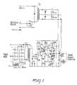
figure 1 is a circuit layout of the high speed driving circuit for MOSFET transistors according to the invention. - With reference to the above figure, the reference sign T1 indicates a first coupling transformer, which is driven on the drive logic side IC1, has a turns ratio equal to 2:1 and is wound with such a method as to have minimal dispersed reactance, although it has a very high immunity to dV/dt, which in this application reaches 10 KV/»sec.
- The circuit furthermore comprises a first stage of the actual driver, indicated by Q1, which is constituted by a small MOSFET transistor with an IDmax of a few hundred mA.
- The first stage Q1 is the most suitable for using the signal which is present on the secondary coil of the first transformer T1 without at the same time excessively loading the logic IC1 and the primary coil.
- The first stage Q1 is furthermore suitable for driving the subsequent second stage, indicated by Q2 and Q3, with rather steep fronts.
- The second stage Q2 and Q3, which is directly coupled to the drain pin of the first stage Q1, is constituted by a pair of medium-power bipolar transistors, for example of the type commercially known by the code BD 137 - BD 138; the pair of medium-power bipolar transistors Q2 and Q3 must be suitable for providing a current with an amplitude sufficient to directly drive two MOSFET transistors of a third stage of the driver which are indicated by Q4 and Q5.
- The third stage of the driver is constituted by two medium-power complementary MOSFET transistors Q4 and Q5, with auxiliary circuitry, indicated in the drawing, which is included essentially in order to reduce the dissipation of the two MOSFET transistors Q4 and Q5, limiting simultaneous conduction and in any case decreasing the "transverse" current, and to drive the final MOSFET transistor according to two distinct paths, thus allowing to easily and independently vary the on and off switching speeds.
- In resonant converters, for example, it is in fact convenient to switch the final MOSFET transistors off very rapidly, whereas switching on can be much slower.
- The driving circuit furthermore has a driver power supply with two voltages, at +12 V and at -3 V with respect to the source pin of the final stage; this has been found to be the best compromise between the need to powerfully drive the final stages, making them immune with respect to oscillations on the gate pin circuit, and containing the dissipation on the two MOSFET transistors Q4 and Q5 of the third stage.
- The power supplies are provided by means of a second ferrite transformer, indicated by the T2, which operates at 100 KHz; the transformer T2 is built so as to have good insulation and a rather low capacitance between the primary and secondary multiturn coils without penalizing it excessively with a high dispersed reactance.
- It has thus been observed that the invention has achieved the intended aim and objects, a high speed driving circuit for MOSFET transistors having been obtained which, by virtue of the use of four drivers, driven by an adequate control logic IC1, and with four final MOSFET transistors with adequate characteristics, has allowed to provide a full-bridge circuit which operates at 2.5 MHz and can handle power up to approximately 2.4 KW.
- The invention is naturally susceptible to numerous modifications and variations, all of which are within the scope of the claims.
- Where technical features mentioned in any claim are followed by reference signs, those reference signs have been included for the sole purpose of increasing the intelligibility of the claims and accordingly such reference signs do not have any limiting effect on the scope of each element identified by way of example by such reference signs.
Claims (9)
- High speed driving circuit for MOSFET transistors comprising:
a first coupling transformer (T1) which is driven at its primary coil and has a turns ratio of 2:1, said turns being wound such that said first coupling transformer has a minimal reactance and very high immunity to dV/dt; and
a first stage (Q1);
characterized in that said driving circuit further comprises a second stage (Q2,Q3) and a third stage (Q4,Q5),
said first stage (Q1) being constituted by a small MOSFET transistor, said first stage (Q1) being adapted for using a signal which is present on the second coil of said first coupling transformer (T1) for driving a second stage (Q2,Q3) without at the same time excessively loading the primary coil of said first coupling transformer (T1);
said second stage (Q2,Q3) being directly coupled to the drain terminal of said first stage (Q1), such as to be driven by said first stage (Q1), said second stage (Q2,Q3) being adapted to provide for a current with an amplitude sufficient to directly drive said third stage (Q4,Q5);
said third stage (Q4,Q5) for driving a final MOSFET transistor, said third stage (Q4,Q5) being supplied with two distinct voltages, said two distinct voltages being provided by a second transformer (T2). - Circuit according to claim 1, characterized in that said first coupling transformer (T1) is driven at its primary coil by means of two HC-MOS quadruple buffers (IC1) in full-bridge connection.
- Circuit according to claims 1 and 2, characterized in that said dV/dt reaches values which are approximately equal to 10 KV/»sec.
- Circuit according to one or more of claims 1-3, characterized in that said small MOSFET transistor of said first stage (Q1) has an IDmax value of a few hundred mA, said small MOSFET transistor using the signal which is present on the secondary coil of said first coupling transformer (T1).
- Circuit according to claims one or more of claims 1-4, characterized in that said second stage (Q2,Q3) is constituted by a pair of medium-power bipolar transistors (Q2,Q3).
- Circuit according to one or more of claims 1-5, characterized in that said third stage is comprised of two complementary medium-power MOSFET transistors (Q4,Q5) which are connected to an auxiliary circuitry (R1,R2,R3,R4, R5,D21,D22,C1,C2,C3,C4) which is adapted to reduce dissipation, to reduce a transverse current between said complementary medium-power MOSFET transistors (Q4,Q5) and to drive a final MOSFET transistor according to two distinct paths in order to independently and easily vary the switching speed during switching on and switching off.
- Circuit according to one or more of claims 1-6, characterized in that said drive circuit can be supplied with voltages at +12 V and -3 V with respect to the source pin of said final MOSFET transistor.
- Circuit according to one or more of claims 1-7, characterized in that said second transformer (T2) is made of ferrite, preferably operates at 100 KHz, has good insulation, a reduced capacitance between the primary and secondary coils, and a modest dispersed reactance.
- Circuit according to one or more of the preceding claims, characterized in that said auxiliary circuitry is comprised of a plurality of resistors (R1,R2,R3,R4, R5), capacitors (C1,C2,C3,C4) and diodes (D21,D22).
Applications Claiming Priority (2)
| Application Number | Priority Date | Filing Date | Title |
|---|---|---|---|
| IT8253990 | 1990-03-19 | ||
| IT82539AIT1240906B (en) | 1990-03-19 | 1990-03-19 | VERY FAST PILOT CIRCUIT FOR MOSFETS |
Publications (3)
| Publication Number | Publication Date |
|---|---|
| EP0447989A2 EP0447989A2 (en) | 1991-09-25 |
| EP0447989A3 EP0447989A3 (en) | 1992-02-26 |
| EP0447989B1true EP0447989B1 (en) | 1995-08-09 |
Family
ID=11318573
Family Applications (1)
| Application Number | Title | Priority Date | Filing Date |
|---|---|---|---|
| EP91104045AExpired - LifetimeEP0447989B1 (en) | 1990-03-19 | 1991-03-15 | High speed driving circuit for MOSFET transistors |
Country Status (4)
| Country | Link |
|---|---|
| EP (1) | EP0447989B1 (en) |
| AT (1) | ATE126409T1 (en) |
| DE (1) | DE69111860T2 (en) |
| IT (1) | IT1240906B (en) |
Families Citing this family (4)
| Publication number | Priority date | Publication date | Assignee | Title |
|---|---|---|---|---|
| FR2718904B1 (en)* | 1994-04-14 | 1996-05-15 | Commissariat Energie Atomique | High voltage fast switch with pulse amplifier. |
| IL118264A (en)* | 1995-06-07 | 2001-03-19 | Kollmorgen Corp | Controller for a brushless motor and a power supply for the controller |
| DE102004057807B4 (en)* | 2004-11-30 | 2013-10-24 | Puls Gmbh | Circuit arrangement for controlling a transformer and method for operating the circuit arrangement |
| JP5488550B2 (en)* | 2011-08-19 | 2014-05-14 | 株式会社安川電機 | Gate drive circuit and power conversion device |
Family Cites Families (2)
| Publication number | Priority date | Publication date | Assignee | Title |
|---|---|---|---|---|
| EP0177148A3 (en)* | 1984-08-29 | 1987-06-03 | Unisys Corporation | Power supplies using mosfet devices |
| GB8713384D0 (en)* | 1987-06-08 | 1987-07-15 | Philips Electronic Associated | Driving semiconductor device |
- 1990
- 1990-03-19ITIT82539Apatent/IT1240906B/enactiveIP Right Grant
- 1991
- 1991-03-15DEDE69111860Tpatent/DE69111860T2/ennot_activeExpired - Fee Related
- 1991-03-15EPEP91104045Apatent/EP0447989B1/ennot_activeExpired - Lifetime
- 1991-03-15ATAT91104045Tpatent/ATE126409T1/ennot_activeIP Right Cessation
Non-Patent Citations (1)
| Title |
|---|
| EPE 3RD EUROPEAN CONFERENCE ON POWER ELECTRONICS AND APLLICATIONS, 9-12 October 1989, Aachen, DE, pp. 165-169 ; H.C. Lovatt et al. : "Design of a 3-phase, MOSFET inverter and associated gate-drive circuit"* |
Also Published As
| Publication number | Publication date |
|---|---|
| IT9082539A1 (en) | 1991-09-19 |
| EP0447989A2 (en) | 1991-09-25 |
| DE69111860D1 (en) | 1995-09-14 |
| EP0447989A3 (en) | 1992-02-26 |
| DE69111860T2 (en) | 1995-12-21 |
| ATE126409T1 (en) | 1995-08-15 |
| IT1240906B (en) | 1993-12-20 |
| IT9082539A0 (en) | 1990-03-19 |
Similar Documents
| Publication | Publication Date | Title |
|---|---|---|
| US20220116033A1 (en) | High voltage nanosecond pulser | |
| US4860189A (en) | Full bridge power converter circuit | |
| EP1356575B1 (en) | Isolated drive circuitry used in switch-mode power converters | |
| US7236041B2 (en) | Isolated gate driver circuit for power switching devices | |
| EP0614267B1 (en) | Lossless active snubber for half-bridge output rectifiers | |
| US4511815A (en) | Transformer-isolated power MOSFET driver circuit | |
| KR100458358B1 (en) | Lamp operation circuit device | |
| US4970620A (en) | FET bridge protection circuit | |
| US5822199A (en) | Controller for a power switch and method of operation thereof | |
| US6108219A (en) | DC power converter circuit | |
| CN101102086B (en) | switch drive circuit | |
| WO1993000744A1 (en) | A 0-100 % duty cycle, transformer isolated fet driver | |
| EP0447989B1 (en) | High speed driving circuit for MOSFET transistors | |
| US20220286127A1 (en) | Bipolar pulsed-voltage gate driver | |
| US20030164721A1 (en) | Gate drive circuitry | |
| US4689731A (en) | MOSFET inverter gate drive circuit | |
| US5410190A (en) | Circuit for shortening the turn-off time of a power transistor | |
| EP1361652A2 (en) | Switching circuit | |
| KR20010039729A (en) | Circuit arrangement | |
| US12149159B2 (en) | Driving circuit of power devices, switching circuit and power conversion circuit | |
| EP4478614A1 (en) | Power semiconductor bridge leg arrangement | |
| WO2025166884A1 (en) | A gate driving circuit for wide bandgap (wbg) power devices | |
| JPH05244764A (en) | Drive circuit of insulted-gate type power semiconductor element | |
| KR100740355B1 (en) | Isolated Gate Driver Circuit for Power Switching Devices | |
| Bourguiba et al. | Gate driver circuit for IGBT using reduced number of high frequency transformers |
Legal Events
| Date | Code | Title | Description |
|---|---|---|---|
| PUAI | Public reference made under article 153(3) epc to a published international application that has entered the european phase | Free format text:ORIGINAL CODE: 0009012 | |
| AK | Designated contracting states | Kind code of ref document:A2 Designated state(s):AT BE CH DE DK ES FR GB GR IT LI LU NL SE | |
| PUAL | Search report despatched | Free format text:ORIGINAL CODE: 0009013 | |
| AK | Designated contracting states | Kind code of ref document:A3 Designated state(s):AT BE CH DE DK ES FR GB GR IT LI LU NL SE | |
| 17P | Request for examination filed | Effective date:19920724 | |
| 17Q | First examination report despatched | Effective date:19940331 | |
| GRAA | (expected) grant | Free format text:ORIGINAL CODE: 0009210 | |
| AK | Designated contracting states | Kind code of ref document:B1 Designated state(s):AT BE CH DE DK ES FR GB GR IT LI LU NL SE | |
| PG25 | Lapsed in a contracting state [announced via postgrant information from national office to epo] | Ref country code:NL Free format text:LAPSE BECAUSE OF FAILURE TO SUBMIT A TRANSLATION OF THE DESCRIPTION OR TO PAY THE FEE WITHIN THE PRESCRIBED TIME-LIMIT Effective date:19950809 Ref country code:LI Effective date:19950809 Ref country code:GR Free format text:LAPSE BECAUSE OF FAILURE TO SUBMIT A TRANSLATION OF THE DESCRIPTION OR TO PAY THE FEE WITHIN THE PRESCRIBED TIME-LIMIT Effective date:19950809 Ref country code:FR Free format text:THE PATENT HAS BEEN ANNULLED BY A DECISION OF A NATIONAL AUTHORITY Effective date:19950809 Ref country code:ES Free format text:THE PATENT HAS BEEN ANNULLED BY A DECISION OF A NATIONAL AUTHORITY Effective date:19950809 Ref country code:DK Effective date:19950809 Ref country code:CH Effective date:19950809 Ref country code:BE Effective date:19950809 | |
| REF | Corresponds to: | Ref document number:126409 Country of ref document:AT Date of ref document:19950815 Kind code of ref document:T | |
| REF | Corresponds to: | Ref document number:69111860 Country of ref document:DE Date of ref document:19950914 | |
| ITF | It: translation for a ep patent filed | ||
| PG25 | Lapsed in a contracting state [announced via postgrant information from national office to epo] | Ref country code:SE Effective date:19951109 | |
| NLV1 | Nl: lapsed or annulled due to failure to fulfill the requirements of art. 29p and 29m of the patents act | ||
| EN | Fr: translation not filed | ||
| PG25 | Lapsed in a contracting state [announced via postgrant information from national office to epo] | Ref country code:GB Effective date:19960315 | |
| PG25 | Lapsed in a contracting state [announced via postgrant information from national office to epo] | Ref country code:LU Free format text:LAPSE BECAUSE OF NON-PAYMENT OF DUE FEES Effective date:19960331 | |
| PLBE | No opposition filed within time limit | Free format text:ORIGINAL CODE: 0009261 | |
| STAA | Information on the status of an ep patent application or granted ep patent | Free format text:STATUS: NO OPPOSITION FILED WITHIN TIME LIMIT | |
| 26N | No opposition filed | ||
| GBPC | Gb: european patent ceased through non-payment of renewal fee | Effective date:19960315 | |
| PGFP | Annual fee paid to national office [announced via postgrant information from national office to epo] | Ref country code:AT Payment date:19980326 Year of fee payment:8 | |
| PGFP | Annual fee paid to national office [announced via postgrant information from national office to epo] | Ref country code:DE Payment date:19980420 Year of fee payment:8 | |
| PG25 | Lapsed in a contracting state [announced via postgrant information from national office to epo] | Ref country code:AT Free format text:LAPSE BECAUSE OF NON-PAYMENT OF DUE FEES Effective date:19990315 | |
| PG25 | Lapsed in a contracting state [announced via postgrant information from national office to epo] | Ref country code:DE Free format text:LAPSE BECAUSE OF NON-PAYMENT OF DUE FEES Effective date:20000101 | |
| PG25 | Lapsed in a contracting state [announced via postgrant information from national office to epo] | Ref country code:IT Free format text:LAPSE BECAUSE OF NON-PAYMENT OF DUE FEES;WARNING: LAPSES OF ITALIAN PATENTS WITH EFFECTIVE DATE BEFORE 2007 MAY HAVE OCCURRED AT ANY TIME BEFORE 2007. THE CORRECT EFFECTIVE DATE MAY BE DIFFERENT FROM THE ONE RECORDED. Effective date:20050315 |