EP0442490A1 - Method for producing single crystal boron nitride film - Google Patents
Method for producing single crystal boron nitride filmDownload PDFInfo
- Publication number
- EP0442490A1 EP0442490A1EP91102090AEP91102090AEP0442490A1EP 0442490 A1EP0442490 A1EP 0442490A1EP 91102090 AEP91102090 AEP 91102090AEP 91102090 AEP91102090 AEP 91102090AEP 0442490 A1EP0442490 A1EP 0442490A1
- Authority
- EP
- European Patent Office
- Prior art keywords
- raw material
- film
- substrate
- vacuum chamber
- boron nitride
- Prior art date
- Legal status (The legal status is an assumption and is not a legal conclusion. Google has not performed a legal analysis and makes no representation as to the accuracy of the status listed.)
- Granted
Links
- 229910052582BNInorganic materials0.000titleclaimsabstractdescription20
- PZNSFCLAULLKQX-UHFFFAOYSA-NBoron nitrideChemical compoundN#BPZNSFCLAULLKQX-UHFFFAOYSA-N0.000titleclaimsabstractdescription20
- 238000004519manufacturing processMethods0.000titleclaimsdescription7
- 239000013078crystalSubstances0.000titleabstractdescription13
- 239000002994raw materialSubstances0.000claimsabstractdescription90
- 239000000758substrateSubstances0.000claimsabstractdescription67
- 239000007789gasSubstances0.000claimsabstractdescription44
- ZOXJGFHDIHLPTG-UHFFFAOYSA-NBoronChemical group[B]ZOXJGFHDIHLPTG-UHFFFAOYSA-N0.000claimsabstractdescription34
- 125000004433nitrogen atomChemical groupN*0.000claimsabstractdescription17
- 238000010926purgeMethods0.000claimsabstractdescription8
- 229910015148B2H6Inorganic materials0.000claimsdescription29
- 238000000034methodMethods0.000claimsdescription20
- XKRFYHLGVUSROY-UHFFFAOYSA-NArgonChemical compound[Ar]XKRFYHLGVUSROY-UHFFFAOYSA-N0.000claimsdescription8
- ILAHWRKJUDSMFH-UHFFFAOYSA-Nboron tribromideChemical compoundBrB(Br)BrILAHWRKJUDSMFH-UHFFFAOYSA-N0.000claimsdescription6
- 239000001257hydrogenSubstances0.000claimsdescription5
- 229910052739hydrogenInorganic materials0.000claimsdescription5
- 229910015844BCl3Inorganic materials0.000claimsdescription4
- 229910052786argonInorganic materials0.000claimsdescription4
- WTEOIRVLGSZEPR-UHFFFAOYSA-Nboron trifluorideChemical compoundFB(F)FWTEOIRVLGSZEPR-UHFFFAOYSA-N0.000claimsdescription4
- FAQYAMRNWDIXMY-UHFFFAOYSA-NtrichloroboraneChemical compoundClB(Cl)ClFAQYAMRNWDIXMY-UHFFFAOYSA-N0.000claimsdescription4
- 229910015845BBr3Inorganic materials0.000claimsdescription3
- 229910015900BF3Inorganic materials0.000claimsdescription3
- UFHFLCQGNIYNRP-UHFFFAOYSA-NHydrogenChemical compound[H][H]UFHFLCQGNIYNRP-UHFFFAOYSA-N0.000claimsdescription2
- 229910052796boronInorganic materials0.000description24
- QJGQUHMNIGDVPM-UHFFFAOYSA-Nnitrogen groupChemical group[N]QJGQUHMNIGDVPM-UHFFFAOYSA-N0.000description12
- 229910003460diamondInorganic materials0.000description11
- 239000010432diamondSubstances0.000description11
- IJGRMHOSHXDMSA-UHFFFAOYSA-NAtomic nitrogenChemical compoundN#NIJGRMHOSHXDMSA-UHFFFAOYSA-N0.000description10
- 150000001875compoundsChemical class0.000description8
- 239000012808vapor phaseSubstances0.000description7
- 239000000463materialSubstances0.000description6
- 229910052757nitrogenInorganic materials0.000description6
- 230000015572biosynthetic processEffects0.000description5
- 238000001451molecular beam epitaxyMethods0.000description5
- 239000002052molecular layerSubstances0.000description5
- 238000003786synthesis reactionMethods0.000description5
- 238000001069Raman spectroscopyMethods0.000description4
- 238000002441X-ray diffractionMethods0.000description4
- 125000004435hydrogen atomChemical class[H]*0.000description4
- CSCPPACGZOOCGX-UHFFFAOYSA-NAcetoneChemical compoundCC(C)=OCSCPPACGZOOCGX-UHFFFAOYSA-N0.000description3
- 101000635799Homo sapiens Run domain Beclin-1-interacting and cysteine-rich domain-containing proteinProteins0.000description3
- 102100030852Run domain Beclin-1-interacting and cysteine-rich domain-containing proteinHuman genes0.000description3
- 125000004429atomChemical group0.000description3
- 238000000151depositionMethods0.000description3
- 230000008021depositionEffects0.000description3
- 239000012071phaseSubstances0.000description3
- 238000005240physical vapour depositionMethods0.000description3
- 238000005268plasma chemical vapour depositionMethods0.000description3
- 238000002128reflection high energy electron diffractionMethods0.000description3
- 239000004065semiconductorSubstances0.000description3
- WGPCGCOKHWGKJJ-UHFFFAOYSA-NsulfanylidenezincChemical compound[Zn]=SWGPCGCOKHWGKJJ-UHFFFAOYSA-N0.000description3
- 238000002230thermal chemical vapour depositionMethods0.000description3
- 238000005979thermal decomposition reactionMethods0.000description3
- OKTJSMMVPCPJKN-UHFFFAOYSA-NCarbonChemical compound[C]OKTJSMMVPCPJKN-UHFFFAOYSA-N0.000description2
- KRHYYFGTRYWZRS-UHFFFAOYSA-NFluoraneChemical compoundFKRHYYFGTRYWZRS-UHFFFAOYSA-N0.000description2
- VEXZGXHMUGYJMC-UHFFFAOYSA-NHydrochloric acidChemical compoundClVEXZGXHMUGYJMC-UHFFFAOYSA-N0.000description2
- KFZMGEQAYNKOFK-UHFFFAOYSA-NIsopropanolChemical compoundCC(C)OKFZMGEQAYNKOFK-UHFFFAOYSA-N0.000description2
- 238000006243chemical reactionMethods0.000description2
- 238000005229chemical vapour depositionMethods0.000description2
- 238000010438heat treatmentMethods0.000description2
- 239000001307heliumSubstances0.000description2
- 229910052734heliumInorganic materials0.000description2
- SWQJXJOGLNCZEY-UHFFFAOYSA-Nhelium atomChemical compound[He]SWQJXJOGLNCZEY-UHFFFAOYSA-N0.000description2
- 230000006698inductionEffects0.000description2
- 238000007733ion platingMethods0.000description2
- 150000004767nitridesChemical class0.000description2
- -1nitrogen-containing compoundChemical class0.000description2
- 239000002243precursorSubstances0.000description2
- 230000009257reactivityEffects0.000description2
- 229920006395saturated elastomerPolymers0.000description2
- 238000001228spectrumMethods0.000description2
- 238000004544sputter depositionMethods0.000description2
- 238000001308synthesis methodMethods0.000description2
- 229910052984zinc sulfideInorganic materials0.000description2
- 229910015241B3N3H6Inorganic materials0.000description1
- 238000004566IR spectroscopyMethods0.000description1
- GRYLNZFGIOXLOG-UHFFFAOYSA-NNitric acidChemical compoundO[N+]([O-])=OGRYLNZFGIOXLOG-UHFFFAOYSA-N0.000description1
- XSTXAVWGXDQKEL-UHFFFAOYSA-NTrichloroethyleneChemical groupClC=C(Cl)ClXSTXAVWGXDQKEL-UHFFFAOYSA-N0.000description1
- 229910003481amorphous carbonInorganic materials0.000description1
- QZPSXPBJTPJTSZ-UHFFFAOYSA-Naqua regiaChemical compoundCl.O[N+]([O-])=OQZPSXPBJTPJTSZ-UHFFFAOYSA-N0.000description1
- JBANFLSTOJPTFW-UHFFFAOYSA-Nazane;boronChemical compound[B].NJBANFLSTOJPTFW-UHFFFAOYSA-N0.000description1
- 229910052799carbonInorganic materials0.000description1
- 150000001722carbon compoundsChemical class0.000description1
- 230000015556catabolic processEffects0.000description1
- 239000007795chemical reaction productSubstances0.000description1
- 238000007796conventional methodMethods0.000description1
- 238000010494dissociation reactionMethods0.000description1
- 230000005593dissociationsEffects0.000description1
- 230000005684electric fieldEffects0.000description1
- 238000011156evaluationMethods0.000description1
- 230000005284excitationEffects0.000description1
- 230000005281excited stateEffects0.000description1
- 238000000171gas-source molecular beam epitaxyMethods0.000description1
- 229910002804graphiteInorganic materials0.000description1
- 239000010439graphiteSubstances0.000description1
- 238000009413insulationMethods0.000description1
- 150000002500ionsChemical class0.000description1
- 239000002184metalSubstances0.000description1
- 238000002488metal-organic chemical vapour depositionMethods0.000description1
- 125000002496methyl groupChemical group[H]C([H])([H])*0.000description1
- 238000002156mixingMethods0.000description1
- 229910052754neonInorganic materials0.000description1
- GKAOGPIIYCISHV-UHFFFAOYSA-Nneon atomChemical compound[Ne]GKAOGPIIYCISHV-UHFFFAOYSA-N0.000description1
- 229910017604nitric acidInorganic materials0.000description1
- 239000003960organic solventSubstances0.000description1
- 238000002360preparation methodMethods0.000description1
- 239000000047productSubstances0.000description1
- 238000006557surface reactionMethods0.000description1
- 238000004227thermal crackingMethods0.000description1
- 230000007704transitionEffects0.000description1
- UBOXGVDOUJQMTN-UHFFFAOYSA-NtrichloroethyleneNatural productsClCC(Cl)ClUBOXGVDOUJQMTN-UHFFFAOYSA-N0.000description1
- LALRXNPLTWZJIJ-UHFFFAOYSA-NtriethylboraneChemical compoundCCB(CC)CCLALRXNPLTWZJIJ-UHFFFAOYSA-N0.000description1
- WXRGABKACDFXMG-UHFFFAOYSA-NtrimethylboraneChemical compoundCB(C)CWXRGABKACDFXMG-UHFFFAOYSA-N0.000description1
- 229910021642ultra pure waterInorganic materials0.000description1
- 239000012498ultrapure waterSubstances0.000description1
- 238000004506ultrasonic cleaningMethods0.000description1
- 238000007740vapor depositionMethods0.000description1
Images


Classifications
- C—CHEMISTRY; METALLURGY
- C30—CRYSTAL GROWTH
- C30B—SINGLE-CRYSTAL GROWTH; UNIDIRECTIONAL SOLIDIFICATION OF EUTECTIC MATERIAL OR UNIDIRECTIONAL DEMIXING OF EUTECTOID MATERIAL; REFINING BY ZONE-MELTING OF MATERIAL; PRODUCTION OF A HOMOGENEOUS POLYCRYSTALLINE MATERIAL WITH DEFINED STRUCTURE; SINGLE CRYSTALS OR HOMOGENEOUS POLYCRYSTALLINE MATERIAL WITH DEFINED STRUCTURE; AFTER-TREATMENT OF SINGLE CRYSTALS OR A HOMOGENEOUS POLYCRYSTALLINE MATERIAL WITH DEFINED STRUCTURE; APPARATUS THEREFOR
- C30B29/00—Single crystals or homogeneous polycrystalline material with defined structure characterised by the material or by their shape
- C30B29/10—Inorganic compounds or compositions
- C30B29/40—AIIIBV compounds wherein A is B, Al, Ga, In or Tl and B is N, P, As, Sb or Bi
- C30B29/403—AIII-nitrides
- C—CHEMISTRY; METALLURGY
- C23—COATING METALLIC MATERIAL; COATING MATERIAL WITH METALLIC MATERIAL; CHEMICAL SURFACE TREATMENT; DIFFUSION TREATMENT OF METALLIC MATERIAL; COATING BY VACUUM EVAPORATION, BY SPUTTERING, BY ION IMPLANTATION OR BY CHEMICAL VAPOUR DEPOSITION, IN GENERAL; INHIBITING CORROSION OF METALLIC MATERIAL OR INCRUSTATION IN GENERAL
- C23C—COATING METALLIC MATERIAL; COATING MATERIAL WITH METALLIC MATERIAL; SURFACE TREATMENT OF METALLIC MATERIAL BY DIFFUSION INTO THE SURFACE, BY CHEMICAL CONVERSION OR SUBSTITUTION; COATING BY VACUUM EVAPORATION, BY SPUTTERING, BY ION IMPLANTATION OR BY CHEMICAL VAPOUR DEPOSITION, IN GENERAL
- C23C16/00—Chemical coating by decomposition of gaseous compounds, without leaving reaction products of surface material in the coating, i.e. chemical vapour deposition [CVD] processes
- C23C16/22—Chemical coating by decomposition of gaseous compounds, without leaving reaction products of surface material in the coating, i.e. chemical vapour deposition [CVD] processes characterised by the deposition of inorganic material, other than metallic material
- C23C16/30—Deposition of compounds, mixtures or solid solutions, e.g. borides, carbides, nitrides
- C23C16/34—Nitrides
- C23C16/342—Boron nitride
- C—CHEMISTRY; METALLURGY
- C23—COATING METALLIC MATERIAL; COATING MATERIAL WITH METALLIC MATERIAL; CHEMICAL SURFACE TREATMENT; DIFFUSION TREATMENT OF METALLIC MATERIAL; COATING BY VACUUM EVAPORATION, BY SPUTTERING, BY ION IMPLANTATION OR BY CHEMICAL VAPOUR DEPOSITION, IN GENERAL; INHIBITING CORROSION OF METALLIC MATERIAL OR INCRUSTATION IN GENERAL
- C23C—COATING METALLIC MATERIAL; COATING MATERIAL WITH METALLIC MATERIAL; SURFACE TREATMENT OF METALLIC MATERIAL BY DIFFUSION INTO THE SURFACE, BY CHEMICAL CONVERSION OR SUBSTITUTION; COATING BY VACUUM EVAPORATION, BY SPUTTERING, BY ION IMPLANTATION OR BY CHEMICAL VAPOUR DEPOSITION, IN GENERAL
- C23C16/00—Chemical coating by decomposition of gaseous compounds, without leaving reaction products of surface material in the coating, i.e. chemical vapour deposition [CVD] processes
- C23C16/44—Chemical coating by decomposition of gaseous compounds, without leaving reaction products of surface material in the coating, i.e. chemical vapour deposition [CVD] processes characterised by the method of coating
- C23C16/455—Chemical coating by decomposition of gaseous compounds, without leaving reaction products of surface material in the coating, i.e. chemical vapour deposition [CVD] processes characterised by the method of coating characterised by the method used for introducing gases into reaction chamber or for modifying gas flows in reaction chamber
- C23C16/45523—Pulsed gas flow or change of composition over time
- C23C16/45525—Atomic layer deposition [ALD]
- C23C16/45527—Atomic layer deposition [ALD] characterized by the ALD cycle, e.g. different flows or temperatures during half-reactions, unusual pulsing sequence, use of precursor mixtures or auxiliary reactants or activations
- C23C16/45531—Atomic layer deposition [ALD] characterized by the ALD cycle, e.g. different flows or temperatures during half-reactions, unusual pulsing sequence, use of precursor mixtures or auxiliary reactants or activations specially adapted for making ternary or higher compositions
- C—CHEMISTRY; METALLURGY
- C23—COATING METALLIC MATERIAL; COATING MATERIAL WITH METALLIC MATERIAL; CHEMICAL SURFACE TREATMENT; DIFFUSION TREATMENT OF METALLIC MATERIAL; COATING BY VACUUM EVAPORATION, BY SPUTTERING, BY ION IMPLANTATION OR BY CHEMICAL VAPOUR DEPOSITION, IN GENERAL; INHIBITING CORROSION OF METALLIC MATERIAL OR INCRUSTATION IN GENERAL
- C23C—COATING METALLIC MATERIAL; COATING MATERIAL WITH METALLIC MATERIAL; SURFACE TREATMENT OF METALLIC MATERIAL BY DIFFUSION INTO THE SURFACE, BY CHEMICAL CONVERSION OR SUBSTITUTION; COATING BY VACUUM EVAPORATION, BY SPUTTERING, BY ION IMPLANTATION OR BY CHEMICAL VAPOUR DEPOSITION, IN GENERAL
- C23C16/00—Chemical coating by decomposition of gaseous compounds, without leaving reaction products of surface material in the coating, i.e. chemical vapour deposition [CVD] processes
- C23C16/44—Chemical coating by decomposition of gaseous compounds, without leaving reaction products of surface material in the coating, i.e. chemical vapour deposition [CVD] processes characterised by the method of coating
- C23C16/455—Chemical coating by decomposition of gaseous compounds, without leaving reaction products of surface material in the coating, i.e. chemical vapour deposition [CVD] processes characterised by the method of coating characterised by the method used for introducing gases into reaction chamber or for modifying gas flows in reaction chamber
- C23C16/45523—Pulsed gas flow or change of composition over time
- C23C16/45525—Atomic layer deposition [ALD]
- C23C16/45527—Atomic layer deposition [ALD] characterized by the ALD cycle, e.g. different flows or temperatures during half-reactions, unusual pulsing sequence, use of precursor mixtures or auxiliary reactants or activations
- C23C16/45536—Use of plasma, radiation or electromagnetic fields
- C23C16/45542—Plasma being used non-continuously during the ALD reactions
- C—CHEMISTRY; METALLURGY
- C30—CRYSTAL GROWTH
- C30B—SINGLE-CRYSTAL GROWTH; UNIDIRECTIONAL SOLIDIFICATION OF EUTECTIC MATERIAL OR UNIDIRECTIONAL DEMIXING OF EUTECTOID MATERIAL; REFINING BY ZONE-MELTING OF MATERIAL; PRODUCTION OF A HOMOGENEOUS POLYCRYSTALLINE MATERIAL WITH DEFINED STRUCTURE; SINGLE CRYSTALS OR HOMOGENEOUS POLYCRYSTALLINE MATERIAL WITH DEFINED STRUCTURE; AFTER-TREATMENT OF SINGLE CRYSTALS OR A HOMOGENEOUS POLYCRYSTALLINE MATERIAL WITH DEFINED STRUCTURE; APPARATUS THEREFOR
- C30B25/00—Single-crystal growth by chemical reaction of reactive gases, e.g. chemical vapour-deposition growth
- C30B25/02—Epitaxial-layer growth
- C30B25/14—Feed and outlet means for the gases; Modifying the flow of the reactive gases
Definitions
- the present inventionrelates to a method for producing a cubic boron nitride film, which can be applied to semiconductor devices such as a diode, a transistor and a sensor, an insulating film or a cemented carbide tool.
- Boron nitrideis a compound consisting of nitrogen and boron atoms and includes various structures such as cubic boron nitride (c-BN), hexagonal boron nitride (h-BN), turbostratic boron nitride (t-BN) and amorphous boron. nitride (a-BN).
- h-BNhas a structure in which plural hexagonal plane structure layers are piled up in the c-axis direction.
- t-BNhas a turbulent structure of h-BN.
- c-BNhas a zinc-blende crystal structure and is a cubic system compound. That is, at a face center position, one of the atoms is present, and the other atom is present at positions such as 1/4, 1/4, 1/4, etc.
- Baron nitrideis a compound similar to carbon. Roughly speaking, h-BN, a-BN and c-BN correspond to graphite, amorphous carbon and diamond, respectively. Boron nitride has similar properties to those of the corresponding carbon compound. As diamond is difficult to synthesize, among the BN compound, c-BN is most difficult to synthesize.
- c-BNis expected as a material to be used in a wide variety of applications.
- c-BNis a promising material as a wide band gap semiconductor which can be doped to form a p-type or n-type semiconductor. More specifically, it is expected as an element of an environment resistant device, a power device or a light emitting device in a range from ultraviolet to blue by utilizing its high heat resistance, high dielectric breakdown electric field and large thermal conductivity.
- c-BNforms an insulating film having good insulating property and thermal conductivity and may be used as a layer insulation film of a device.
- a c-BN single crystalhas been produced only by a high pressure synthesis method. It was reported that a prototype pn-junction diode was produced from doped c-BN bulk, exhibited rectification even at a high temperature of 500°C or higher and emitted light in a range from ultraviolet to visible light at forward bias (cf. Mishima et al, Applied Physics Letters, 53 [11] 962-964 (1988)).
- the presently produced c-BN crystalis a particulate crystal produced by the high pressure synthesis method. Hitherto, no c-BN film has been produced.
- c-BN filmsThere are may reports on the preparation of c-BN films. However, the films do not consist of the c-BN phase only. The reported BN films contain microcrystalline c-BN phases partly, and no wholly crystalline c-BN film has been prepared.
- One object of the present inventionis to provide a boron nitride film whole of which consists of crystalline c-BN.
- Another object of the present inventionis to provide a method for producing a boron nitride film whole of which consists of crystalline c-BN.
- a method for producing a cubic boron nitride filmcomprising alternately supplying a raw material gas comprising boron atoms and a raw material gas comprising nitrogen atoms in a vacuum chamber to form a cubic boron nitride film on a heated substrate and evacuating the vacuum chamber when one raw material gas is switched to the other to prevent coexistence of the both raw materials in the vacuum chamber.
- a method for producing a cubic boron nitride filmcomprising alternately supplying a raw material gas comprising boron atoms and a raw material gas comprising nitrogen atoms in a vacuum chamber to form a cubic boron nitride film on a heated substrate and evacuating the vacuum chamber and purging the vacuum chamber with a gas which is inactive with the raw materials when one raw material gas is switched to the other to prevent coexistence of the both raw materials in the vacuum chamber.
- Fig. 1shows an example of a c-BN film growing program according to the present invention, in which B2H6 is used as the boron-containing raw material gas, and NH3 is used as the nitrogen-containing raw material gas.
- the axes of abscissa and ordinaterepresent a time and flow rates of the raw material gasses to be supplied in the vacuum chamber, respectively.
- the graphs (a) and (b)correspond to the flow rates of B2H6 and NH3, respectively.
- B2H6is supplied for a certain time period ( ⁇ B6H6). Then, the vacuum chamber is throughly evacuated for a certain time period ( ⁇ VAC1 ). Thereafter, NH3 is supplied for a certain time period ( ⁇ NH3) and again the vacuum chamber is evacuated for a certain time period ( ⁇ VAC2 ). These supply of the raw material gases and evacuation procedures are repeated to produce the crystalline c-BN film.
- One cycle Tis a sum of ⁇ B2H6 , ⁇ VAC1 , ⁇ NH3 and ⁇ VAC2 . Accordingly, only one raw material is present in the chamber and the both raw materials do not coexist at any moment. This is one of the characteristics of the present invention.
- the vacuum chamberis purged with a gas which is inactive with the raw materials such as hydrogen or argon for a certain time period ( ⁇ H2 in Fig. 2).
- first B2H6is supplied for a certain time period ( ⁇ B6H6 ). Then, the vacuum chamber is thoroughly evacuated for a certain time period ( ⁇ VAC1 ) and a purging gas (H2) is introduced for a certain time period ( ⁇ H2). After evacuating H2 for a certain time period ( ⁇ VAC2 ), NH3 is supplied for a certain time period ( ⁇ NH3 ). Further, the vacuum chamber is evacuated for a certain time period ( ⁇ VAC3 ), H2 is introduced in the vacuum chamber for a certain time period ( ⁇ H2 ) and the vacuum chamber is evacuated ( ⁇ VAC4 ). These supply, evacuation and purging procedures are repeated to produce the crystalline c-BN film.
- One cycle Tis a sum of ⁇ B2H6 , ⁇ NH3 ⁇ ⁇ H2 and all the evacuation time periods.
- Examples of the purging gasare hydrogen, helium, argon and the like, which are inactive to the raw material gasses.
- Examples of the boron-containing raw materialare B2H6, BF3, BCl3, BBr3, B(CH3)3, B(C2H5)3, etc.
- nitrogen-containing raw materialexamples include NH3, N2, NF3, etc.
- These raw materialsmay be diluted with hydrogen, helium, argon, neon, etc.
- each raw material gas as suchcan be supplied in the vacuum chamber, it may be dissociated or excited by thermal cracking, plasma or UV light before supplied on the substrate.
- the boron or nitrogen atoms in the raw material gasare in the excited state, their reactivity is increased. Thereby, quality of the produced c-BN film is improved, and the substrate temperature can be lowered.
- the substrate temperatureis preferably from 300 to 1400°C, more preferably from 400 to 1100°C during vapor phase synthesis.
- vapor phase synthesisincludes the CVD methods such as a molecular beam epitaxial growing method, thermal CVD, RF plasma CVD, microwave CVD, etc. and the PVD methods such as ion vapor deposition, ion plating, activated reactive deposition, sputtering, etc.
- the baron-containing raw material and the nitrogen-containing raw materialare simultaneously supplied on the substrate in both the CVD and PVD methods.
- the baron-containing compound and the nitrogen-containing compoundhave very high reactivity with each other, and a reaction product has mainly a bond with the sp2 orbital. This product forms a h-BN precursor having a layer structure through the sp2 bonds.
- B2H6-NH3As one example, a B2H6-NH3 system will be explained.
- B2H6 and NH3easily react each other in a temperature range between room temperature and 200°C to form various compounds such as BH3NH3 (borazane), (BH2NH2) x (borazene) and B3N3H6 (borazol). These compounds liberate the hydrogen atoms by heating and are converted to h-BN. Then, from these compounds, c-BN is not formed. Therefore, when the boron and nitrogen atoms coexist, h-BN with lower energy is formed.
- h-BNis formed at a temperature higher than 1000°C or 1200°C.
- h-BNmay tend to be formed even when the raw materials are dissociated or excited by a plasma or a laser beam.
- the crystalline c-BN filmis not produced since the precursor of h-BN is easily formed by the vapor phase reaction.
- the boron-containing raw material and the nitrogen-containing raw materialare alternately supplied, whereby the vapor phase reaction between the two raw materials are completely prevented.
- the c-BN layeris formed layer by layer through a surface reaction of the raw materials which are adsorbed on the substrate. This layer-by-layer growth of the c-BN film will be explained below.
- c-BNhas a crystalline structure of the zincblende structure.
- a substrateis made of a material which has a crystalline structure such as the zincblende structure, a diamond structure, a face-centered cubic lattice structure or a tetrahedral (sp3) structure (for example, the wurtzite structure)
- the grown layersucceeds the crystalline structure of the substrate so that c-BN is predominantly formed.
- a substrate a lattice constant of which is the same as that of c-BN or a substrate having a lattice constant a difference of which from that of c-BN is smallit is preferable to use.
- a c-BN substrate or a diamond substrate which has the lattice constant a difference of which from that of c-BN is only 1.3 %is preferred.
- a plane on which the c-BN film is growna plane in which boron and nitrogen atoms are not present together, for example, a (100) or (111) plane or a plane which has a small off angle from the (100) or (111) plane is preferred, because the method of present invention grow layer by layer the boron layer and the nitrogen layer by supplying alternately the boron-containing raw material and the nitrogen-containing raw material.
- One of the essential features of the present inventionis alternate supply of the boron-containing raw material and the nitrogen-containing raw material. Since c-BN has a special property, c-BN crystal is correctly grown by such alternate supply of the raw materials. Such mechanism is called as a "self-limiting mechanism" in this invention. Since this mechanism is first found by the present inventors, it will be hereinafter explained in detail.
- the c-BN filmis not produced.
- the raw material supplied in one periodshould be adsorbed on the surface of the substrate or the already grown layer in one or two layers, and the film should be grown under conditions suitable for layer-by-layer growth of the film.
- boron atomsare adsorbed in only one or two layers and no additional layer of boron is adsorbed. This also applies to the nitrogen atoms.
- the self-limiting mechanismis the key feature of the method of the present invention.
- Conditions for achieving the self-limiting mechanismdepend on kinds and supplying methods of the raw materials, a kind and plane of the substrate, growth pressure, a substrate temperature and the like. In many cases, the self-limiting mechanism works at a temperature not higher than 1200°C.
- the substrateswere subjected to ultrasonic cleaning in an organic solvent (e.g. isopropanol, acetone, trichloroethylene, etc.) and then treated with hydrochloric acid, hydrofluoric acid/ nitric acid and aqua regia successively, followed by rinsing with ultra-pure water.
- organic solvente.g. isopropanol, acetone, trichloroethylene, etc.
- the substratewas heated to a temperature from 1000°C to 1200°C under high vacuum of 10 ⁇ 8 to 10 ⁇ 4 Torr. to clean its surface.
- MBEgrowing apparatus
- a used apparatuswas a conventional gas source MBE apparatus.
- a substratewas set with a manipulator and rotated with heating.
- a raw material gaswas splashed towards the substrate in the form of a molecular beam.
- two molecular beams of the raw materialswere supplied alternately.
- a boron-containing raw materialB2H6 was used, and as a nitrogen-containing raw material, NH3 was used.
- the B2H6 gasis easily decomposed and polymerized at a comparatively low temperature.
- a substrate temperature of 800 to 1000°Ca boron film is formed. That is, the self-limiting mechanism does not work. Since under such temperature condition, very precise control of the gas flow rate is required, it is difficult to grow a film with good quality. Then, when B2H6 is used as the raw material, a growth temperature should be not higher than 800°C.
- the substrate temperatureis too low, it is difficult to decompose the nitrogen-containing raw material such as NH3 or N2, the nitrogen atoms are not contained in the formed film, or a crystalline film is not formed.
- NH3was precracked with plasma before introducing in the chamber. Thereby, the nitrogen atoms are contained in the formed film even if the substrate temperature is low.
- the precrackingcan be carried out by thermal decomposition or the plasma such as RF plasma or microwave plasma.
- a precracking meansis provided in the up-stream of the ultra-high vacuum growing apparatus. For example, following three precracking apparatus can be used;
- Fig. 9shows a thermal decomposition type precracking apparatus, which comprises an insulating pipe 9 and a heater 2 wound around the pipe 9.
- a reflection plate 3made of a heat resistant metal is provided around the pipe 9 and the heater 2.
- the heater 2is powdered by a heater power source 1 and heats a part of the pipe 9 around which the heater is wound.
- the raw material (NH3)is supplied from one end (the right end in Fig. 9) of the pipe 9 and heated and precracked to form activated species. Since the material is activated, the nitrogen atoms can be dissociated even if the substrate temperature is low.
- Fig. 10shows a PF plasma type precracking apparatus, which comprises an insulating pipe 9 and an induction coil 5 wound around the pipe 9.
- the RF peeris supplied to the induction coil 5 from a radiofrequency power source 4, and the raw material NH3 is decomposed with the RF power to form activated species.
- Fig. 11shows a microwave plasma type precracking apparatus, which comprises a waveguide tube 7 and a variable short-circuit plate 8.
- the insulating pipe 9passes through a part of the waveguide tube 7.
- the raw material NH3flows through the insulating pipe 9, it is decomposed with microwave.
- the growing conditionswere as follows:
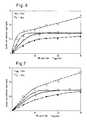
- Figs. 3 and 4are the graphs showing a relationship between the growth rate and ⁇ B2H6 and a relationship between the growth rate and ⁇ NH3 respectively.
- the growth ratemeans a film thickness grown in one cycle of gas flow pulse.
- the growth rateis one (one molecular layer/cycle). with this factor, the growth rates were normalized.
- the black circlesare the results at the substrate temperature of 300°C
- the white circlesare the results at 400°C
- the trianglesare the results at 600°C
- the squaresare the results at 800°C.
- the growth rateincreases in proportional with ⁇ B2H6 when ⁇ B2H6 is small, but saturates at a certain value of ⁇ B2H6 .
- the saturated growth rateis one (1).
- the growth ratesaturates at a single molecular layer and the thickness does not increase. That is, a layer consisting of boron does not grow.
- the growth ratedoes not saturate and increases as ⁇ B2H6 , increases. This means that the boron layer continues to grow.
- the growth rateincreases as ⁇ NH3 increases, but it saturates when ⁇ NH3 is from several seconds to about 30 seconds.
- the saturated growth rateis one (1).
- the growth ratedoes not saturate.
- the film thickness per one pulsesaturates and does not exceed a certain value. This means that, even if the supply amount of the raw material is increased, the growth stops at a single atom layer which is adsorbed on the substrate surface or the previously formed layer.
- the growth rategradually increases as ⁇ B2H6 or ⁇ NH3 increases. This means that, at 800°C, the self-limiting mechanism does not work perfectly. At such high substrate temperature, it is difficult to grow the boron atoms or the nitrogen atoms layer by layer.
- the boron layer and the nitrogen layercan be alternately grown layer by layer.
- the film growthcan be carried out with excellent control.
- a c-BN film of a thickness of about 1 ⁇ mwas grown on a diamond substrate at ⁇ B2H6 of 10 Sec., ⁇ NH3 of 15 Sec. and a substrate temperature of 400°C.
- the Raman spectroscopic spectrum of the produced c-BN filmis shown in Fig. 5.
- the sharp Raman shift peaks of c-BNare observed at 1055 cm ⁇ 1 and 1305 cm ⁇ 1.
- the peak at 1334 cm ⁇ 1is assigned to the diamond of the substrate.
- the spot pattern corresponding to c-BN (100)was obtained. This means that the grown film was the single crystal of c-BN (100).
- the self-limiting mechanismdoes not work perfectly at the high substrate temperature, for instance, 800°C in the above Examples, it is possible to grow the c-BN film by precisely controlling the supply of the raw materials. That is, the c-BN can be formed by selecting ⁇ B2H6 and ⁇ NH3 so that the growth rate is one molecular layer per cycle.
- the conditions which achieve the self-limiting mechanismdepend on the kinds and flow rates of the raw materials, the growth pressure, the kind and temperature of the substrate and the like. For example, when BCl3 is used as a boron-containing raw material or when N2 is used as a nitrogen-containing raw material, a higher substrate temperature is required than the B2H6-NH3 system.
- a used apparatuswas a conventional vacuum thermal CVD apparatus.
- the raw materialis flowed in a gas state without forming the molecular beam as in the MBE, and the pressure is higher than in the case of MBE.
- the substrateis set with facing upward or sideward.
- a boron-containing raw materialtrimethylboron [B(CH3)3] (TMB) was used, and as a nitrogen-containing raw material, NH3 was used.
- TMBtrimethylboron
- NH3nitrogen-containing raw material.
- the growing conditionswere as follows:
- the filmwas grown according to the growth program of Fig. 2. Namely, the chamber was purged by supplying the hydrogen (H2) gas at a flow rate of 5 to 30 sccm between the supply periods of TMB and NH3.
- Figs. 6 and 7show the dependency of the growth rate on ⁇ TMB and ⁇ NH3 when the flow rates of TMB, NH3 and H2 were 3 sccm., 15 sccm. and 20 sccm., respectively and the length of the H2 gas pulse was 10 Sec. There was no material difference of the results in Figs. 6 and 7 between the diamond substrate and the c-BN substrate.
- the condition range in which the self-limiting mechanism works in this examplewas slightly different from those in Example 1. That is, in this example, up to about 1000°C of the substrate temperature, the self-limiting mechanism worked, but at a substrate temperature of 1200°C or higher, the self-limiting mechanism did not work. Such difference is based on the differences of the apparatuses and the raw materials.
- the content of "self-limiting"is also different.
- the growth rate at which the self-limiting mechanism workedwas 0.6 to 0.8 molecular layer per cycle, which was different from the one molecular layer per cycle in Example 1. The reason for this difference is as follow:
- TMBhas three bulky methyl groups, when one molecule is adsorbed on the substrate surface, it interferes adjacent adsorbing sites.
- the growth rate at which the self-limiting mechanism works, namely the film thickness which is obtained in one gas pulsevaries with the raw material gases, the kind of the substrate, and the like.
- the produced filmwas evaluated by IR spectroscopy, Raman spectroscopy, X-ray diffraction and RHEED to find that the film produced under the self-limiting conditions was a single crystal c-BN film.
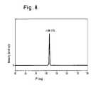
- Fig. 8shows an X-ray diffraction pattern of the film which was grown on the (111) c-BN substrate at ⁇ TMB of 12 sccm, ⁇ NH3 of 15 sccm and the substrate temperature of 1000°C and had a thickness of about 1.5 ⁇ m.
- the grown filmwas a single crystal film of c-BN (111).
- the c-BN filmcan be formed.
Landscapes
- Chemical & Material Sciences (AREA)
- Engineering & Computer Science (AREA)
- Metallurgy (AREA)
- Materials Engineering (AREA)
- Organic Chemistry (AREA)
- Chemical Kinetics & Catalysis (AREA)
- General Chemical & Material Sciences (AREA)
- Mechanical Engineering (AREA)
- Crystallography & Structural Chemistry (AREA)
- Inorganic Chemistry (AREA)
- Physics & Mathematics (AREA)
- Electromagnetism (AREA)
- Plasma & Fusion (AREA)
- Crystals, And After-Treatments Of Crystals (AREA)
- Chemical Vapour Deposition (AREA)
Abstract
Description
- The present invention relates to a method for producing a cubic boron nitride film, which can be applied to semiconductor devices such as a diode, a transistor and a sensor, an insulating film or a cemented carbide tool.
- Boron nitride is a compound consisting of nitrogen and boron atoms and includes various structures such as cubic boron nitride (c-BN), hexagonal boron nitride (h-BN), turbostratic boron nitride (t-BN) and amorphous boron. nitride (a-BN).
- h-BN has a structure in which plural hexagonal plane structure layers are piled up in the c-axis direction. t-BN has a turbulent structure of h-BN. c-BN has a zinc-blende crystal structure and is a cubic system compound. That is, at a face center position, one of the atoms is present, and the other atom is present at positions such as 1/4, 1/4, 1/4, etc.
- Baron nitride is a compound similar to carbon. Roughly speaking, h-BN, a-BN and c-BN correspond to graphite, amorphous carbon and diamond, respectively. Boron nitride has similar properties to those of the corresponding carbon compound. As diamond is difficult to synthesize, among the BN compound, c-BN is most difficult to synthesize.
- c-BN is expected as a material to be used in a wide variety of applications.
- For example, c-BN is a promising material as a wide band gap semiconductor which can be doped to form a p-type or n-type semiconductor. More specifically, it is expected as an element of an environment resistant device, a power device or a light emitting device in a range from ultraviolet to blue by utilizing its high heat resistance, high dielectric breakdown electric field and large thermal conductivity.
- Without doping, c-BN forms an insulating film having good insulating property and thermal conductivity and may be used as a layer insulation film of a device.
- In addition, since c-BN has large hardness, it is promising as a tool material.
- Hitherto, a c-BN single crystal has been produced only by a high pressure synthesis method. It was reported that a prototype pn-junction diode was produced from doped c-BN bulk, exhibited rectification even at a high temperature of 500°C or higher and emitted light in a range from ultraviolet to visible light at forward bias (cf. Mishima et al, Applied Physics Letters,53 [11] 962-964 (1988)).
- As described above, the presently produced c-BN crystal is a particulate crystal produced by the high pressure synthesis method. Hitherto, no c-BN film has been produced.
- In view of wide application of c-BN, it is essential to produce a c-BN film.
- It has been tried to produce the c-BN film by CVD methods such as thermal CVD, RF plasma CVD and microwave plasma CVD, or by PVD methods such as IVD, ion plating, activated reactive deposition and sputtering. In these methods, a raw material gas containing boron atoms and a raw material gas containing nitrogen atoms are simultaneously supplied on a substrate to synthesize boron nitride. However, none of these methods provide satisfactory results. This is because thermodynamically stable h-BN and/or a BN film having largely disturbed structure are very easily deposited.
- There are may reports on the preparation of c-BN films. However, the films do not consist of the c-BN phase only. The reported BN films contain microcrystalline c-BN phases partly, and no wholly crystalline c-BN film has been prepared.
- One object of the present invention is to provide a boron nitride film whole of which consists of crystalline c-BN.
- Another object of the present invention is to provide a method for producing a boron nitride film whole of which consists of crystalline c-BN.
- According to a first aspect of the present invention, there is provided a method for producing a cubic boron nitride film comprising alternately supplying a raw material gas comprising boron atoms and a raw material gas comprising nitrogen atoms in a vacuum chamber to form a cubic boron nitride film on a heated substrate and evacuating the vacuum chamber when one raw material gas is switched to the other to prevent coexistence of the both raw materials in the vacuum chamber.
- According to a second aspect of the present invention, there is provided a method for producing a cubic boron nitride film comprising alternately supplying a raw material gas comprising boron atoms and a raw material gas comprising nitrogen atoms in a vacuum chamber to form a cubic boron nitride film on a heated substrate and evacuating the vacuum chamber and purging the vacuum chamber with a gas which is inactive with the raw materials when one raw material gas is switched to the other to prevent coexistence of the both raw materials in the vacuum chamber.
- Fig. 1 shows an example of a c-BN film growing program according to the present invention,
- Fig. 2 shows another example of a c-BN film growing program according to the present invention,
- Figs. 3 and 4 are the graphs showing a relationship between the growth rate and τB₂H₆ and a relationship between the growth rate and τNH₃, respectively in Example 1,
- Fig. 5 shows a Raman spectroscopic spectrum of the c-BN film produced in Example 1,
- Figs. 6 and 7 show the dependency of the growth rate on τTMB and τNH₃ in Example 2,
- Fig. 8 shows an X-ray diffraction pattern of the film which was grown on the (111) c-BN substrate in Example 2,
- Fig. 9 shows a thermal decomposition type precracking apparatus,
- Fig. 10 shows a PF plasma type precracking apparatus, and
- Fig. 11 shows a microwave plasma type precracking apparatus,
- Fig. 1 shows an example of a c-BN film growing program according to the present invention, in which B₂H₆ is used as the boron-containing raw material gas, and NH₃ is used as the nitrogen-containing raw material gas. The axes of abscissa and ordinate represent a time and flow rates of the raw material gasses to be supplied in the vacuum chamber, respectively. The graphs (a) and (b) correspond to the flow rates of B₂H₆ and NH₃, respectively.
- First, B₂H₆ is supplied for a certain time period (τB₆H₆). Then, the vacuum chamber is throughly evacuated for a certain time period (τVAC1). Thereafter, NH₃ is supplied for a certain time period (τNH₃) and again the vacuum chamber is evacuated for a certain time period (τVAC2). These supply of the raw material gases and evacuation procedures are repeated to produce the crystalline c-BN film. One cycle T is a sum of τB₂H₆, τVAC1, τNH₃ and τVAC2 . Accordingly, only one raw material is present in the chamber and the both raw materials do not coexist at any moment. This is one of the characteristics of the present invention.
- To further completely prevent the coexistance of the both raw materials, it is preferable to purge the vacuum chamber with a different gas when one raw material gas is switched to the other.
- As shown in Fig. 2, after one of the raw material gasses (B₂H₆ or NH₃) is supplied in the vacuum chamber and the chamber is evacuated and before the other is supplied in the vacuum chamber, the vacuum chamber is purged with a gas which is inactive with the raw materials such as hydrogen or argon for a certain time period (τH₂ in Fig. 2).
- That is, first B₂H₆ is supplied for a certain time period (τB₆H₆). Then, the vacuum chamber is thoroughly evacuated for a certain time period (τVAC1) and a purging gas (H₂) is introduced for a certain time period (τH₂). After evacuating H₂ for a certain time period (τVAC2), NH₃ is supplied for a certain time period (τNH₃). Further, the vacuum chamber is evacuated for a certain time period (τVAC3), H₂ is introduced in the vacuum chamber for a certain time period (τH₂) and the vacuum chamber is evacuated (τVAC4). These supply, evacuation and purging procedures are repeated to produce the crystalline c-BN film. One cycle T is a sum of τB₂H₆, τNH₃ʼ τH₂ and all the evacuation time periods.
- Examples of the purging gas are hydrogen, helium, argon and the like, which are inactive to the raw material gasses.
- Examples of the boron-containing raw material are B₂H₆, BF₃, BCl₃, BBr₃, B(CH₃)₃, B(C₂H₅)₃, etc.
- Examples of the nitrogen-containing raw material are NH₃, N₂, NF₃, etc.
- These raw materials may be diluted with hydrogen, helium, argon, neon, etc.
- Although each raw material gas as such can be supplied in the vacuum chamber, it may be dissociated or excited by thermal cracking, plasma or UV light before supplied on the substrate. By the dissociation or excitation, the boron or nitrogen atoms in the raw material gas are in the excited state, their reactivity is increased. Thereby, quality of the produced c-BN film is improved, and the substrate temperature can be lowered.
- Depending on the kinds of the raw materials and the substrate, the substrate temperature is preferably from 300 to 1400°C, more preferably from 400 to 1100°C during vapor phase synthesis.
- Herein, the term "vapor phase synthesis" is used in a broad meaning. The vapor phase synthesis includes the CVD methods such as a molecular beam epitaxial growing method, thermal CVD, RF plasma CVD, microwave CVD, etc. and the PVD methods such as ion vapor deposition, ion plating, activated reactive deposition, sputtering, etc.
- Now, the mechanism of the present invention will be explained in comparison with the conventional method.
- In the conventional vapor phase synthesis of the c-BN film, the baron-containing raw material and the nitrogen-containing raw material are simultaneously supplied on the substrate in both the CVD and PVD methods. However, the baron-containing compound and the nitrogen-containing compound have very high reactivity with each other, and a reaction product has mainly a bond with the sp² orbital. This product forms a h-BN precursor having a layer structure through the sp² bonds.
- As one example, a B₂H₆-NH₃ system will be explained. B₂H₆ and NH₃ easily react each other in a temperature range between room temperature and 200°C to form various compounds such as BH₃NH₃ (borazane), (BH₂NH₂)x (borazene) and B₃N₃H₆ (borazol). These compounds liberate the hydrogen atoms by heating and are converted to h-BN. Then, from these compounds, c-BN is not formed. Therefore, when the boron and nitrogen atoms coexist, h-BN with lower energy is formed.
- Also, in a B₂H₆-N₂ system, h-BN is formed at a temperature higher than 1000°C or 1200°C.
- h-BN may tend to be formed even when the raw materials are dissociated or excited by a plasma or a laser beam.
- Under the vapor phase synthesis conditions, since h-BN is in the stable state while c-BN is in the unstable state, h-BN is deposited. Once h-BN is formed during the deposition of the BN film, it is never changed to c-BN through phase transition.
- Accordingly, when the boron-containing raw material and the nitrogen-containing raw material are simultaneously supplied, the crystalline c-BN film is not produced since the precursor of h-BN is easily formed by the vapor phase reaction.
- According to the present invention, the boron-containing raw material and the nitrogen-containing raw material are alternately supplied, whereby the vapor phase reaction between the two raw materials are completely prevented. Under such condition, the c-BN layer is formed layer by layer through a surface reaction of the raw materials which are adsorbed on the substrate. This layer-by-layer growth of the c-BN film will be explained below.
- The substrate to be used in the method of the present invention is explained
- c-BN has a crystalline structure of the zincblende structure. When a substrate is made of a material which has a crystalline structure such as the zincblende structure, a diamond structure, a face-centered cubic lattice structure or a tetrahedral (sp³) structure (for example, the wurtzite structure), the grown layer succeeds the crystalline structure of the substrate so that c-BN is predominantly formed.
- To produce the single crystal c-BN film, it is preferable to use a substrate a lattice constant of which is the same as that of c-BN or a substrate having a lattice constant a difference of which from that of c-BN is small. For example, a c-BN substrate or a diamond substrate which has the lattice constant a difference of which from that of c-BN is only 1.3 % is preferred.
- As a plane on which the c-BN film is grown, a plane in which boron and nitrogen atoms are not present together, for example, a (100) or (111) plane or a plane which has a small off angle from the (100) or (111) plane is preferred, because the method of present invention grow layer by layer the boron layer and the nitrogen layer by supplying alternately the boron-containing raw material and the nitrogen-containing raw material.
- One of the essential features of the present invention is alternate supply of the boron-containing raw material and the nitrogen-containing raw material. Since c-BN has a special property, c-BN crystal is correctly grown by such alternate supply of the raw materials. Such mechanism is called as a "self-limiting mechanism" in this invention. Since this mechanism is first found by the present inventors, it will be hereinafter explained in detail.
- If plural layers of the boron layers and/or the nitrogen layers are formed during the supply of the boron-containing raw material or the nitrogen-containing raw material, the c-BN film is not produced. The raw material supplied in one period should be adsorbed on the surface of the substrate or the already grown layer in one or two layers, and the film should be grown under conditions suitable for layer-by-layer growth of the film.
- In case of the growth of c-BN, when one raw material gas is supplied in a specific temperature range, only one or two layers are adsorbed with respect to the specific element (B or N) contained in the supplied raw material, and further supply of the same raw material gas does not form third and subsequent layers. Namely, the growth of the layers is automatically stopped. Such property is called as the "self-limiting mechanism".
- For example, when the boron-containing raw material is supplied in the absence of nitrogen atoms, boron atoms are adsorbed in only one or two layers and no additional layer of boron is adsorbed. This also applies to the nitrogen atoms.
- The self-limiting mechanism is the key feature of the method of the present invention.
- Conditions for achieving the self-limiting mechanism depend on kinds and supplying methods of the raw materials, a kind and plane of the substrate, growth pressure, a substrate temperature and the like. In many cases, the self-limiting mechanism works at a temperature not higher than 1200°C.
- The present invention will be illustrated by following Examples.
- In Examples, two types of apparatuses were used, one of which was (1) an ultra-high vacuum growing (molecular beam epitaxy, MBE) apparatus and the other of which was (2) a vacuum CVD growing apparatus. These apparatuses are known ones.
- Used substrate were
- (i) High-pressure synthesized Ib diamond substrate (3 mm square, 0.3 mm thick), and
- (ii) High-pressure synthesized undoped c-BN substrate (1.5 mm square, 0.3 mm thick).
- Before setting in the apparatus, the substrates were subjected to ultrasonic cleaning in an organic solvent (e.g. isopropanol, acetone, trichloroethylene, etc.) and then treated with hydrochloric acid, hydrofluoric acid/ nitric acid and aqua regia successively, followed by rinsing with ultra-pure water.
- Just before supplying a raw material gas, the substrate was heated to a temperature from 1000°C to 1200°C under high vacuum of 10⁻⁸ to 10⁻⁴ Torr. to clean its surface.
- A used apparatus was a conventional gas source MBE apparatus. In a chamber kept at ultra-high vacuum, a substrate was set with a manipulator and rotated with heating. From a molecular beam cell set below the substrate, a raw material gas was splashed towards the substrate in the form of a molecular beam. By alternately opening and closing valves, two molecular beams of the raw materials were supplied alternately. As a boron-containing raw material, B₂H₆ was used, and as a nitrogen-containing raw material, NH₃ was used.
- The B₂H₆ gas is easily decomposed and polymerized at a comparatively low temperature. When it is supplied at a substrate temperature of 800 to 1000°C, a boron film is formed. That is, the self-limiting mechanism does not work. Since under such temperature condition, very precise control of the gas flow rate is required, it is difficult to grow a film with good quality. Then, when B₂H₆ is used as the raw material, a growth temperature should be not higher than 800°C.
- If the substrate temperature is too low, it is difficult to decompose the nitrogen-containing raw material such as NH₃ or N₂, the nitrogen atoms are not contained in the formed film, or a crystalline film is not formed.
- Thus, in this example, NH₃ was precracked with plasma before introducing in the chamber. Thereby, the nitrogen atoms are contained in the formed film even if the substrate temperature is low.
- The precracking can be carried out by thermal decomposition or the plasma such as RF plasma or microwave plasma.
- A precracking means is provided in the up-stream of the ultra-high vacuum growing apparatus. For example, following three precracking apparatus can be used;
- Fig. 9 shows a thermal decomposition type precracking apparatus, which comprises an insulating
pipe 9 and aheater 2 wound around thepipe 9. Around thepipe 9 and theheater 2, areflection plate 3 made of a heat resistant metal is provided. Theheater 2 is powdered by aheater power source 1 and heats a part of thepipe 9 around which the heater is wound. - The raw material (NH₃) is supplied from one end (the right end in Fig. 9) of the
pipe 9 and heated and precracked to form activated species. Since the material is activated, the nitrogen atoms can be dissociated even if the substrate temperature is low. - Fig. 10 shows a PF plasma type precracking apparatus, which comprises an insulating
pipe 9 and aninduction coil 5 wound around thepipe 9. The RF peer is supplied to theinduction coil 5 from a radiofrequency power source 4, and the raw material NH₃ is decomposed with the RF power to form activated species. - Fig. 11 shows a microwave plasma type precracking apparatus, which comprises a waveguide tube 7 and a variable short-
circuit plate 8. The insulatingpipe 9 passes through a part of the waveguide tube 7. When the raw material NH₃ flows through the insulatingpipe 9, it is decomposed with microwave. - In this Example, the apparatus of Fig. 11 was used, and NH₃ was precracked with the microwave plasma (2.45 GHz) and introduced in the growing apparatus to grow the c-BN film.
- The growing conditions were as follows:
- Flow rates:
- B₂H₆ = 0.1 to 3.0 sccm NH₃ = 0.1 to 10 sccm.
- Back pressure:
- 2 x 10⁻¹⁰ Torr.
- Growing pressure:
- 5 x 10⁻⁶ to 3 x 10⁻⁴ Torr.
- Substrate temperature:
- 300 to 800°C.
- Microwave power for precracking :
- 150 W
- Substrate:
- Ultra-high pressure synthesized diamond Ib with the (100) plane.
- First, the self-limiting mechanism was studied.
- At the flow rates of 0.5 sccm and 1.5 sccm of B₂H₆ and NH₃, respectively, a film was formed according to the growth program of Fig. 1.
- As described above, between each supply periods of B₂H₆ and NH₃, the chamber was evacuated to prevent the mixing of the two raw materials. Dependency of a growing rate on τB₂H₆ and τNH₃ was examined with varying τNH₃ and τB₂H₆.
- The results are shown in Figs. 3 and 4, which are the graphs showing a relationship between the growth rate and τB₂H₆ and a relationship between the growth rate and τNH₃ respectively.
- Here, the growth rate means a film thickness grown in one cycle of gas flow pulse. when each one layer of boron and nitrogen of the c-BN layer is grown, the growth rate is one (one molecular layer/cycle). with this factor, the growth rates were normalized.
- In Figs. 3 and 4, the black circles are the results at the substrate temperature of 300°C, the white circles are the results at 400°C, the triangles are the results at 600°C, and the squares are the results at 800°C.
- As seen from Fig. 3, at the substrate temperature of from 300 to 600°C, the growth rate increases in proportional with τB₂H₆ when τB₂H₆ is small, but saturates at a certain value of τB₂H₆. The saturated growth rate is one (1). In this substrate temperature range, the growth rate saturates at a single molecular layer and the thickness does not increase. That is, a layer consisting of boron does not grow.
- At 800°C, the growth rate does not saturate and increases as τB₂H₆, increases. This means that the boron layer continues to grow.
- The above applies to NH₃. AS seen from Fig. 4, at the substrate temperature of from 300 to 600°C, the growth rate increases as τNH₃ increases, but it saturates when τNH₃ is from several seconds to about 30 seconds. The saturated growth rate is one (1). At the substrate temperature of 800°C or higher, the growth rate does not saturate.
- Even when τNH₃ or τB₂H₆ is increased, the film thickness per one pulse saturates and does not exceed a certain value. This means that, even if the supply amount of the raw material is increased, the growth stops at a single atom layer which is adsorbed on the substrate surface or the previously formed layer.
- when the substrate temperature is 800°C, the growth rate gradually increases as τB₂H₆ or τNH₃ increases. This means that, at 800°C, the self-limiting mechanism does not work perfectly. At such high substrate temperature, it is difficult to grow the boron atoms or the nitrogen atoms layer by layer.
- Under the conditions under which the self-limiting mechanism works, The boron layer and the nitrogen layer can be alternately grown layer by layer. Thus, under such conditions, the film growth can be carried out with excellent control.
- All of the films grown under such conditions were the single crystal c-BN films.
- As an example, a c-BN film of a thickness of about 1 µm was grown on a diamond substrate at τB₂H₆ of 10 Sec., τNH₃ of 15 Sec. and a substrate temperature of 400°C. The Raman spectroscopic spectrum of the produced c-BN film is shown in Fig. 5. The sharp Raman shift peaks of c-BN are observed at 1055 cm⁻¹ and 1305 cm⁻¹. The peak at 1334 cm⁻¹ is assigned to the diamond of the substrate.
- According to evaluation by RHEED, the spot pattern corresponding to c-BN (100) was obtained. This means that the grown film was the single crystal of c-BN (100).
- In addition, the X-ray diffraction analysis confirmed the growth of c-BN (100).
- Though the self-limiting mechanism does not work perfectly at the high substrate temperature, for instance, 800°C in the above Examples, it is possible to grow the c-BN film by precisely controlling the supply of the raw materials. That is, the c-BN can be formed by selecting τB₂H₆ and τNH₃ so that the growth rate is one molecular layer per cycle.
- The conditions which achieve the self-limiting mechanism depend on the kinds and flow rates of the raw materials, the growth pressure, the kind and temperature of the substrate and the like. For example, when BCl₃ is used as a boron-containing raw material or when N₂ is used as a nitrogen-containing raw material, a higher substrate temperature is required than the B₂H₆-NH₃ system.
- A used apparatus was a conventional vacuum thermal CVD apparatus. In this apparatus, the raw material is flowed in a gas state without forming the molecular beam as in the MBE, and the pressure is higher than in the case of MBE. The substrate is set with facing upward or sideward. As a boron-containing raw material, trimethylboron [B(CH₃)₃] (TMB) was used, and as a nitrogen-containing raw material, NH₃ was used. The growing conditions were as follows:
- Flow rates;
- TMB; 2 to 30 sccm. MH₃: 2 to 100 sccm.
- Pressure:
- 0.1 to 30 Torr.
- Substrate temperature:
- 300 to 1300°C.
- Substrates:
- High pressure synthesized diamond 1b (111) or High pressure synthesized c-BN (111).
- The film was grown according to the growth program of Fig. 2. Namely, the chamber was purged by supplying the hydrogen (H₂) gas at a flow rate of 5 to 30 sccm between the supply periods of TMB and NH₃.
- In the same procedures as in Example 1, the self-limiting mechanism was studied.
- Figs. 6 and 7 show the dependency of the growth rate on τTMB and τNH₃ when the flow rates of TMB, NH₃ and H₂ were 3 sccm., 15 sccm. and 20 sccm., respectively and the length of the H₂ gas pulse was 10 Sec. There was no material difference of the results in Figs. 6 and 7 between the diamond substrate and the c-BN substrate.
- As seen from the results of Figs. 6 and 7, the complete saturation of the growth rate was observed in the temperature range between 600°C and 1000°C in relation to τTMB and τNH₃. This means that the self-limiting mechanism worked.
- The condition range in which the self-limiting mechanism works in this example was slightly different from those in Example 1. That is, in this example, up to about 1000°C of the substrate temperature, the self-limiting mechanism worked, but at a substrate temperature of 1200°C or higher, the self-limiting mechanism did not work. Such difference is based on the differences of the apparatuses and the raw materials.
- The content of "self-limiting" is also different. The growth rate at which the self-limiting mechanism worked was 0.6 to 0.8 molecular layer per cycle, which was different from the one molecular layer per cycle in Example 1. The reason for this difference is as follow:
- Since TMB has three bulky methyl groups, when one molecule is adsorbed on the substrate surface, it interferes adjacent adsorbing sites. The growth rate at which the self-limiting mechanism works, namely the film thickness which is obtained in one gas pulse varies with the raw material gases, the kind of the substrate, and the like.
- The produced film was evaluated by IR spectroscopy, Raman spectroscopy, X-ray diffraction and RHEED to find that the film produced under the self-limiting conditions was a single crystal c-BN film.
- Both on the (111) diamond substrate and the (111) c-BN substrate, the single crystal (111) c-BN grew epitaxially.
- For example, Fig. 8 shows an X-ray diffraction pattern of the film which was grown on the (111) c-BN substrate at τTMB of 12 sccm, τNH₃ of 15 sccm and the substrate temperature of 1000°C and had a thickness of about 1.5 µm.
- At 2ϑ of 43.3°, a sharp peak assigned to the (111) plane of c-BN was observed. There was no peak to be assigned to the (200) or (220) plane of c-BN.
- In the RHEED, a spot pattern of the (111) plane of c-BN was obtained.
- From these results, the grown film was a single crystal film of c-BN (111).
- Even if the substrate temperature is high so that the self-limiting mechanism does not work, the precise control of the flow rates of the raw material gases makes it possible to grow the c-BN film as in Example 1.
- When triethylboron [B(C₂H₅)₃] or boron fluoride (BF₃) is used in place of TMB, the c-BN film can be formed.
Claims (9)
- A method for producing a cubic boron nitride film comprising alternately supplying a raw material gas comprising boron atoms and a raw material gas comprising nitrogen atoms in a vacuum chamber to form a cubic boron nitride film on a heated substrate and evacuating the vacuum chamber when one raw material gas is switched to the other to prevent coexistence of the both raw materials in the vacuum chamber.
- The method according to claim 1, wherein a temperature of the substrate is from 300 to 1400°C.
- The method according to claim 1, wherein the raw material comprising the boron atoms is selected from the group consisting, of B₂H₆, BF₃, BCl₃, BBr₃, B(CH₃)₃ and B(C₂H₅)₃.
- The method according to claim 1, wherein the raw material comprising the nitrogen atoms is selected from the group consistingof NH₃, N₂ and NF₃.
- A method for producing a cubic boron nitride film comprising alternately supplying a raw material gas comprising boron atoms and a raw material gas comprising nitrogen atoms in a vacuum chamber to form a cubic boron nitride film on a heated substrate and evacuating the vacuum chamber and purging the vacuum chamber with a gas which is inactive with the raw materials when one raw material gas is switched to the other to prevent coexistence of the both raw materials in the vacuum chamber.
- The method according to claim 5, wherein a temperature of the substrate is from 300 to 1400°C.
- The method according to claim 5, wherein the raw material comprising the boron atoms is selected from the group consisting of B₂H₆, BF₃, BCl₃, BBr₃, B(CH₃)₃ and B(C₂H₅)₃.
- The method according to claim 5, wherein the raw material comprising the nitrogen atoms is selected from the group consistingof NH₃, N₂ and NF₃.
- The method according to claim 5, wherein a purging gas is hydrogen or argon.
Applications Claiming Priority (2)
| Application Number | Priority Date | Filing Date | Title |
|---|---|---|---|
| JP32973/90 | 1990-02-14 | ||
| JP2032973AJP2822536B2 (en) | 1990-02-14 | 1990-02-14 | Method for forming cubic boron nitride thin film |
Publications (2)
| Publication Number | Publication Date |
|---|---|
| EP0442490A1true EP0442490A1 (en) | 1991-08-21 |
| EP0442490B1 EP0442490B1 (en) | 1995-05-03 |
Family
ID=12373837
Family Applications (1)
| Application Number | Title | Priority Date | Filing Date |
|---|---|---|---|
| EP19910102090Expired - LifetimeEP0442490B1 (en) | 1990-02-14 | 1991-02-14 | Method for producing single crystal boron nitride film |
Country Status (3)
| Country | Link |
|---|---|
| EP (1) | EP0442490B1 (en) |
| JP (1) | JP2822536B2 (en) |
| DE (1) | DE69109329T2 (en) |
Cited By (67)
| Publication number | Priority date | Publication date | Assignee | Title |
|---|---|---|---|---|
| WO2000061833A1 (en)* | 1999-04-14 | 2000-10-19 | Arthur Sherman | Sequential chemical vapor deposition |
| WO2001029280A1 (en)* | 1999-10-15 | 2001-04-26 | Asm America, Inc. | Deposition of transition metal carbides |
| US6451695B2 (en) | 1999-03-11 | 2002-09-17 | Genus, Inc. | Radical-assisted sequential CVD |
| US6482262B1 (en) | 1959-10-10 | 2002-11-19 | Asm Microchemistry Oy | Deposition of transition metal carbides |
| WO2002099860A1 (en)* | 2001-05-31 | 2002-12-12 | Midwest Research Institute | Method of preparing nitrogen containing semiconductor material |
| US6503330B1 (en) | 1999-12-22 | 2003-01-07 | Genus, Inc. | Apparatus and method to achieve continuous interface and ultrathin film during atomic layer deposition |
| US6511539B1 (en) | 1999-09-08 | 2003-01-28 | Asm America, Inc. | Apparatus and method for growth of a thin film |
| WO2002080228A3 (en)* | 2001-04-02 | 2003-02-27 | Motorola Inc | Structure including cubic boron nitride films |
| US6551399B1 (en) | 2000-01-10 | 2003-04-22 | Genus Inc. | Fully integrated process for MIM capacitors using atomic layer deposition |
| US6599572B2 (en) | 2000-01-18 | 2003-07-29 | Asm Microchemistry Oy | Process for growing metalloid thin films utilizing boron-containing reducing agents |
| US6617173B1 (en) | 2000-10-11 | 2003-09-09 | Genus, Inc. | Integration of ferromagnetic films with ultrathin insulating film using atomic layer deposition |
| US6620670B2 (en) | 2002-01-18 | 2003-09-16 | Applied Materials, Inc. | Process conditions and precursors for atomic layer deposition (ALD) of AL2O3 |
| US6620723B1 (en) | 2000-06-27 | 2003-09-16 | Applied Materials, Inc. | Formation of boride barrier layers using chemisorption techniques |
| EP1039512A3 (en)* | 1999-03-23 | 2003-11-05 | Matsushita Electric Industrial Co., Ltd. | Method for growing semiconductor film by pulsed chemical vapour deposition |
| US6660126B2 (en) | 2001-03-02 | 2003-12-09 | Applied Materials, Inc. | Lid assembly for a processing system to facilitate sequential deposition techniques |
| US6734020B2 (en) | 2001-03-07 | 2004-05-11 | Applied Materials, Inc. | Valve control system for atomic layer deposition chamber |
| US6765178B2 (en) | 2000-12-29 | 2004-07-20 | Applied Materials, Inc. | Chamber for uniform substrate heating |
| US6811814B2 (en) | 2001-01-16 | 2004-11-02 | Applied Materials, Inc. | Method for growing thin films by catalytic enhancement |
| US6825447B2 (en) | 2000-12-29 | 2004-11-30 | Applied Materials, Inc. | Apparatus and method for uniform substrate heating and contaminate collection |
| US6855368B1 (en) | 2000-06-28 | 2005-02-15 | Applied Materials, Inc. | Method and system for controlling the presence of fluorine in refractory metal layers |
| US6951804B2 (en) | 2001-02-02 | 2005-10-04 | Applied Materials, Inc. | Formation of a tantalum-nitride layer |
| US6986914B2 (en) | 2001-09-14 | 2006-01-17 | Asm International N.V. | Metal nitride deposition by ALD with reduction pulse |
| US6998579B2 (en) | 2000-12-29 | 2006-02-14 | Applied Materials, Inc. | Chamber for uniform substrate heating |
| US7085616B2 (en) | 2001-07-27 | 2006-08-01 | Applied Materials, Inc. | Atomic layer deposition apparatus |
| US7087497B2 (en) | 2004-03-04 | 2006-08-08 | Applied Materials | Low-thermal-budget gapfill process |
| US7097886B2 (en) | 2002-12-13 | 2006-08-29 | Applied Materials, Inc. | Deposition process for high aspect ratio trenches |
| US7101795B1 (en) | 2000-06-28 | 2006-09-05 | Applied Materials, Inc. | Method and apparatus for depositing refractory metal layers employing sequential deposition techniques to form a nucleation layer |
| US7211144B2 (en) | 2001-07-13 | 2007-05-01 | Applied Materials, Inc. | Pulsed nucleation deposition of tungsten layers |
| EP1788117A1 (en)* | 2005-11-18 | 2007-05-23 | United Technologies Corporation | Multilayered boron nitride/silicon nitride coatings |
| US7262133B2 (en) | 2003-01-07 | 2007-08-28 | Applied Materials, Inc. | Enhancement of copper line reliability using thin ALD tan film to cap the copper line |
| US7399388B2 (en) | 2003-07-25 | 2008-07-15 | Applied Materials, Inc. | Sequential gas flow oxide deposition technique |
| US7399357B2 (en) | 2003-05-08 | 2008-07-15 | Arthur Sherman | Atomic layer deposition using multilayers |
| US7405158B2 (en) | 2000-06-28 | 2008-07-29 | Applied Materials, Inc. | Methods for depositing tungsten layers employing atomic layer deposition techniques |
| US7405143B2 (en) | 2004-03-25 | 2008-07-29 | Asm International N.V. | Method for fabricating a seed layer |
| US7427571B2 (en) | 2004-10-15 | 2008-09-23 | Asm International, N.V. | Reactor design for reduced particulate generation |
| US7553516B2 (en) | 2005-12-16 | 2009-06-30 | Asm International N.V. | System and method of reducing particle contamination of semiconductor substrates |
| US7595270B2 (en) | 2007-01-26 | 2009-09-29 | Asm America, Inc. | Passivated stoichiometric metal nitride films |
| US7598170B2 (en) | 2007-01-26 | 2009-10-06 | Asm America, Inc. | Plasma-enhanced ALD of tantalum nitride films |
| US7629256B2 (en) | 2007-05-14 | 2009-12-08 | Asm International N.V. | In situ silicon and titanium nitride deposition |
| US7666474B2 (en) | 2008-05-07 | 2010-02-23 | Asm America, Inc. | Plasma-enhanced pulsed deposition of metal carbide films |
| US7674726B2 (en) | 2004-10-15 | 2010-03-09 | Asm International N.V. | Parts for deposition reactors |
| US7691757B2 (en) | 2006-06-22 | 2010-04-06 | Asm International N.V. | Deposition of complex nitride films |
| US7732350B2 (en) | 2004-09-22 | 2010-06-08 | Asm International N.V. | Chemical vapor deposition of TiN films in a batch reactor |
| US7780788B2 (en) | 2001-10-26 | 2010-08-24 | Applied Materials, Inc. | Gas delivery apparatus for atomic layer deposition |
| US7833906B2 (en) | 2008-12-11 | 2010-11-16 | Asm International N.V. | Titanium silicon nitride deposition |
| US8076242B2 (en) | 2008-05-07 | 2011-12-13 | Asm Genitech Korea Ltd. | Methods of forming an amorphous silicon thin film |
| US8268409B2 (en) | 2006-10-25 | 2012-09-18 | Asm America, Inc. | Plasma-enhanced deposition of metal carbide films |
| US8815709B2 (en) | 2008-10-03 | 2014-08-26 | Veeco Instruments Inc. | Chemical vapor deposition with energy input |
| CN105143503A (en)* | 2012-12-21 | 2015-12-09 | 普拉萨德·纳哈·加吉尔 | Low temperature deposition method of ceramic thin film |
| US9631272B2 (en) | 2008-04-16 | 2017-04-25 | Asm America, Inc. | Atomic layer deposition of metal carbide films using aluminum hydrocarbon compounds |
| US9704716B2 (en) | 2013-03-13 | 2017-07-11 | Asm Ip Holding B.V. | Deposition of smooth metal nitride films |
| US9786491B2 (en) | 2015-11-12 | 2017-10-10 | Asm Ip Holding B.V. | Formation of SiOCN thin films |
| US9786492B2 (en) | 2015-11-12 | 2017-10-10 | Asm Ip Holding B.V. | Formation of SiOCN thin films |
| US9831094B2 (en) | 2005-10-27 | 2017-11-28 | Asm International N.V. | Enhanced thin film deposition |
| US9941425B2 (en) | 2015-10-16 | 2018-04-10 | Asm Ip Holdings B.V. | Photoactive devices and materials |
| US10002936B2 (en) | 2014-10-23 | 2018-06-19 | Asm Ip Holding B.V. | Titanium aluminum and tantalum aluminum thin films |
| US10504901B2 (en) | 2017-04-26 | 2019-12-10 | Asm Ip Holding B.V. | Substrate processing method and device manufactured using the same |
| US10513772B2 (en) | 2009-10-20 | 2019-12-24 | Asm International N.V. | Process for passivating dielectric films |
| US10600637B2 (en) | 2016-05-06 | 2020-03-24 | Asm Ip Holding B.V. | Formation of SiOC thin films |
| US10643925B2 (en) | 2014-04-17 | 2020-05-05 | Asm Ip Holding B.V. | Fluorine-containing conductive films |
| US10847529B2 (en) | 2017-04-13 | 2020-11-24 | Asm Ip Holding B.V. | Substrate processing method and device manufactured by the same |
| US10991573B2 (en) | 2017-12-04 | 2021-04-27 | Asm Ip Holding B.V. | Uniform deposition of SiOC on dielectric and metal surfaces |
| US11158500B2 (en) | 2017-05-05 | 2021-10-26 | Asm Ip Holding B.V. | Plasma enhanced deposition processes for controlled formation of oxygen containing thin films |
| US12142479B2 (en) | 2020-01-17 | 2024-11-12 | Asm Ip Holding B.V. | Formation of SiOCN thin films |
| US12341005B2 (en) | 2020-01-17 | 2025-06-24 | Asm Ip Holding B.V. | Formation of SiCN thin films |
| US12354877B2 (en) | 2020-06-24 | 2025-07-08 | Asm Ip Holding B.V. | Vapor deposition of films comprising molybdenum |
| US12359315B2 (en) | 2019-02-14 | 2025-07-15 | Asm Ip Holding B.V. | Deposition of oxides and nitrides |
Families Citing this family (11)
| Publication number | Priority date | Publication date | Assignee | Title |
|---|---|---|---|---|
| US7732327B2 (en) | 2000-06-28 | 2010-06-08 | Applied Materials, Inc. | Vapor deposition of tungsten materials |
| US7964505B2 (en) | 2005-01-19 | 2011-06-21 | Applied Materials, Inc. | Atomic layer deposition of tungsten materials |
| DE10143377B4 (en)* | 2001-09-05 | 2005-10-27 | Deutsches Zentrum für Luft- und Raumfahrt e.V. | Microwave reactor and method for controlling reactions of activated molecules |
| US7611751B2 (en) | 2006-11-01 | 2009-11-03 | Asm America, Inc. | Vapor deposition of metal carbide films |
| US7713874B2 (en) | 2007-05-02 | 2010-05-11 | Asm America, Inc. | Periodic plasma annealing in an ALD-type process |
| US8841182B1 (en) | 2013-03-14 | 2014-09-23 | Asm Ip Holding B.V. | Silane and borane treatments for titanium carbide films |
| US8846550B1 (en) | 2013-03-14 | 2014-09-30 | Asm Ip Holding B.V. | Silane or borane treatment of metal thin films |
| US9394609B2 (en) | 2014-02-13 | 2016-07-19 | Asm Ip Holding B.V. | Atomic layer deposition of aluminum fluoride thin films |
| JP6637095B2 (en)* | 2018-03-22 | 2020-01-29 | プラサド ナーハー ガジル | Low temperature deposition method of ceramic thin film |
| US20230261138A1 (en)* | 2020-07-13 | 2023-08-17 | Nippon Telegraph And Telephone Corporation | Light-Emitting Element and Method for Manufacturing the Same |
| JP7479011B2 (en)* | 2020-08-05 | 2024-05-08 | 国立大学法人東海国立大学機構 | Manufacturing method of hexagonal boron nitride thin film |
Citations (1)
| Publication number | Priority date | Publication date | Assignee | Title |
|---|---|---|---|---|
| US3561920A (en)* | 1968-05-31 | 1971-02-09 | Varian Associates | Chemical vapor deposition of thick deposits of isotropic boron nitride |
- 1990
- 1990-02-14JPJP2032973Apatent/JP2822536B2/ennot_activeExpired - Lifetime
- 1991
- 1991-02-14EPEP19910102090patent/EP0442490B1/ennot_activeExpired - Lifetime
- 1991-02-14DEDE1991609329patent/DE69109329T2/ennot_activeExpired - Fee Related
Patent Citations (1)
| Publication number | Priority date | Publication date | Assignee | Title |
|---|---|---|---|---|
| US3561920A (en)* | 1968-05-31 | 1971-02-09 | Varian Associates | Chemical vapor deposition of thick deposits of isotropic boron nitride |
Non-Patent Citations (6)
| Title |
|---|
| APPLIED PHYSICS LETTERS. vol. 53, no. 11, 12 September 1988, NEW YORK US pages 962 - 964; O. MISHIMA ET AL: "Ultraviolet light-emitting diode of a cubic boron nitride pn junction made at high pressure"* |
| JOURNAL OF CRYSTAL GROWTH. vol. 98, no. 1/2, November 1989, AMSTERDAM NL pages 195 - 208; S.P. DenBAARS ET AL: "ATOMIC LAYER EPITAXY OF COMPOUND SEMICONDUCTORS WITH METALORGANIC PRECURSORS"* |
| JOURNAL OF CRYSTAL GROWTH. vol. 99, no. 1/4, January 1990, AMSTERDAM NL pages 346 - 351; N. OHTSUKA ET AL: "A NEW GaAs ON Si STRUCTURE USING AlAs BUFFER LAYERS GROWN BY ATOMIC LAYER EPITAXY"* |
| PATENT ABSTRACTS OF JAPAN vol. 12, no. 143 (C-492)(2990) 30 April 1988, & JP-A-62 260062 (SUMITOMO ELECTRIC IND LTD) 12 November 1987,* |
| PATENT ABSTRACTS OF JAPAN vol. 12, no. 299 (C-520)(3146) 15 August 1988, & JP-A-63 69973 (SUMITOMO ELECTRIC IND LTD) 30 March 1988,* |
| PATENT ABSTRACTS OF JAPAN vol. 13, no. 42 (C-564)(3390) 30 January 1989, & JP-A-63 239197 (YUKIO OSAKA) 05 October 1988,* |
Cited By (119)
| Publication number | Priority date | Publication date | Assignee | Title |
|---|---|---|---|---|
| US6482262B1 (en) | 1959-10-10 | 2002-11-19 | Asm Microchemistry Oy | Deposition of transition metal carbides |
| US7410671B2 (en) | 1996-08-16 | 2008-08-12 | Asm International N.V. | Sequential chemical vapor deposition |
| US6652924B2 (en) | 1996-08-16 | 2003-11-25 | Licensee For Microelectronics: Asm America, Inc. | Sequential chemical vapor deposition |
| US6342277B1 (en) | 1996-08-16 | 2002-01-29 | Licensee For Microelectronics: Asm America, Inc. | Sequential chemical vapor deposition |
| US7682657B2 (en) | 1996-08-16 | 2010-03-23 | Asm International N.V. | Sequential chemical vapor deposition |
| US6616986B2 (en) | 1996-08-16 | 2003-09-09 | Asm America Inc. | Sequential chemical vapor deposition |
| US8323737B2 (en) | 1996-08-16 | 2012-12-04 | Asm International N.V. | Sequential chemical vapor deposition |
| US6451695B2 (en) | 1999-03-11 | 2002-09-17 | Genus, Inc. | Radical-assisted sequential CVD |
| US6475910B1 (en) | 1999-03-11 | 2002-11-05 | Genus, Inc. | Radical-assisted sequential CVD |
| EP1039512A3 (en)* | 1999-03-23 | 2003-11-05 | Matsushita Electric Industrial Co., Ltd. | Method for growing semiconductor film by pulsed chemical vapour deposition |
| KR100818792B1 (en)* | 1999-04-14 | 2008-04-02 | 에이에스엠 인터내셔널 엔.브이. | Seqeuntial Chemical Vapor Deposition |
| EP1462542A1 (en)* | 1999-04-14 | 2004-09-29 | Arthur Sherman | Chemical vapour deposition |
| WO2000061833A1 (en)* | 1999-04-14 | 2000-10-19 | Arthur Sherman | Sequential chemical vapor deposition |
| KR100771257B1 (en)* | 1999-04-14 | 2007-10-29 | 에이에스엠 인터내셔널 엔.브이. | Continuous chemical vapor deposition |
| KR100853008B1 (en)* | 1999-04-14 | 2008-08-19 | 에이에스엠 인터내셔널 엔.브이. | Continuous chemical vapor deposition |
| US6511539B1 (en) | 1999-09-08 | 2003-01-28 | Asm America, Inc. | Apparatus and method for growth of a thin film |
| US7141499B2 (en) | 1999-09-08 | 2006-11-28 | Asm America Inc. | Apparatus and method for growth of a thin film |
| US6764546B2 (en) | 1999-09-08 | 2004-07-20 | Asm International N.V. | Apparatus and method for growth of a thin film |
| EP1216106A4 (en)* | 1999-09-08 | 2005-09-28 | Asm Inc | APPARATUS AND METHOD FOR GROWING A THIN LAYER |
| US7431767B2 (en) | 1999-09-08 | 2008-10-07 | Asm America, Inc. | Apparatus and method for growth of a thin film |
| US7485340B2 (en) | 1999-10-15 | 2009-02-03 | Asm International N.V. | Production of elemental films using a boron-containing reducing agent |
| US6800552B2 (en) | 1999-10-15 | 2004-10-05 | Asm International, N.V. | Deposition of transition metal carbides |
| US6821889B2 (en) | 1999-10-15 | 2004-11-23 | Asm International N.V. | Production of elemental thin films using a boron-containing reducing agent |
| US7144809B2 (en) | 1999-10-15 | 2006-12-05 | Asm International N.V. | Production of elemental films using a boron-containing reducing agent |
| WO2001029280A1 (en)* | 1999-10-15 | 2001-04-26 | Asm America, Inc. | Deposition of transition metal carbides |
| US6503330B1 (en) | 1999-12-22 | 2003-01-07 | Genus, Inc. | Apparatus and method to achieve continuous interface and ultrathin film during atomic layer deposition |
| US6551399B1 (en) | 2000-01-10 | 2003-04-22 | Genus Inc. | Fully integrated process for MIM capacitors using atomic layer deposition |
| US6794287B2 (en) | 2000-01-18 | 2004-09-21 | Asm International Nv | Process for growing metal or metal carbide thin films utilizing boron-containing reducing agents |
| US6599572B2 (en) | 2000-01-18 | 2003-07-29 | Asm Microchemistry Oy | Process for growing metalloid thin films utilizing boron-containing reducing agents |
| US6620723B1 (en) | 2000-06-27 | 2003-09-16 | Applied Materials, Inc. | Formation of boride barrier layers using chemisorption techniques |
| US7405158B2 (en) | 2000-06-28 | 2008-07-29 | Applied Materials, Inc. | Methods for depositing tungsten layers employing atomic layer deposition techniques |
| US6855368B1 (en) | 2000-06-28 | 2005-02-15 | Applied Materials, Inc. | Method and system for controlling the presence of fluorine in refractory metal layers |
| US7033922B2 (en) | 2000-06-28 | 2006-04-25 | Applied Materials. Inc. | Method and system for controlling the presence of fluorine in refractory metal layers |
| US7846840B2 (en) | 2000-06-28 | 2010-12-07 | Applied Materials, Inc. | Method for forming tungsten materials during vapor deposition processes |
| US7101795B1 (en) | 2000-06-28 | 2006-09-05 | Applied Materials, Inc. | Method and apparatus for depositing refractory metal layers employing sequential deposition techniques to form a nucleation layer |
| US6617173B1 (en) | 2000-10-11 | 2003-09-09 | Genus, Inc. | Integration of ferromagnetic films with ultrathin insulating film using atomic layer deposition |
| US6998579B2 (en) | 2000-12-29 | 2006-02-14 | Applied Materials, Inc. | Chamber for uniform substrate heating |
| US7022948B2 (en) | 2000-12-29 | 2006-04-04 | Applied Materials, Inc. | Chamber for uniform substrate heating |
| US6765178B2 (en) | 2000-12-29 | 2004-07-20 | Applied Materials, Inc. | Chamber for uniform substrate heating |
| US6825447B2 (en) | 2000-12-29 | 2004-11-30 | Applied Materials, Inc. | Apparatus and method for uniform substrate heating and contaminate collection |
| US6811814B2 (en) | 2001-01-16 | 2004-11-02 | Applied Materials, Inc. | Method for growing thin films by catalytic enhancement |
| US9012334B2 (en) | 2001-02-02 | 2015-04-21 | Applied Materials, Inc. | Formation of a tantalum-nitride layer |
| US7094680B2 (en) | 2001-02-02 | 2006-08-22 | Applied Materials, Inc. | Formation of a tantalum-nitride layer |
| US7781326B2 (en) | 2001-02-02 | 2010-08-24 | Applied Materials, Inc. | Formation of a tantalum-nitride layer |
| US8114789B2 (en) | 2001-02-02 | 2012-02-14 | Applied Materials, Inc. | Formation of a tantalum-nitride layer |
| US6951804B2 (en) | 2001-02-02 | 2005-10-04 | Applied Materials, Inc. | Formation of a tantalum-nitride layer |
| US6660126B2 (en) | 2001-03-02 | 2003-12-09 | Applied Materials, Inc. | Lid assembly for a processing system to facilitate sequential deposition techniques |
| US7201803B2 (en) | 2001-03-07 | 2007-04-10 | Applied Materials, Inc. | Valve control system for atomic layer deposition chamber |
| US6734020B2 (en) | 2001-03-07 | 2004-05-11 | Applied Materials, Inc. | Valve control system for atomic layer deposition chamber |
| WO2002080228A3 (en)* | 2001-04-02 | 2003-02-27 | Motorola Inc | Structure including cubic boron nitride films |
| WO2002099860A1 (en)* | 2001-05-31 | 2002-12-12 | Midwest Research Institute | Method of preparing nitrogen containing semiconductor material |
| US7211144B2 (en) | 2001-07-13 | 2007-05-01 | Applied Materials, Inc. | Pulsed nucleation deposition of tungsten layers |
| US7085616B2 (en) | 2001-07-27 | 2006-08-01 | Applied Materials, Inc. | Atomic layer deposition apparatus |
| US6986914B2 (en) | 2001-09-14 | 2006-01-17 | Asm International N.V. | Metal nitride deposition by ALD with reduction pulse |
| US7410666B2 (en) | 2001-09-14 | 2008-08-12 | Asm International N.V. | Metal nitride carbide deposition by ALD |
| US8668776B2 (en) | 2001-10-26 | 2014-03-11 | Applied Materials, Inc. | Gas delivery apparatus and method for atomic layer deposition |
| US7780788B2 (en) | 2001-10-26 | 2010-08-24 | Applied Materials, Inc. | Gas delivery apparatus for atomic layer deposition |
| US6620670B2 (en) | 2002-01-18 | 2003-09-16 | Applied Materials, Inc. | Process conditions and precursors for atomic layer deposition (ALD) of AL2O3 |
| US7097886B2 (en) | 2002-12-13 | 2006-08-29 | Applied Materials, Inc. | Deposition process for high aspect ratio trenches |
| US7262133B2 (en) | 2003-01-07 | 2007-08-28 | Applied Materials, Inc. | Enhancement of copper line reliability using thin ALD tan film to cap the copper line |
| US7399357B2 (en) | 2003-05-08 | 2008-07-15 | Arthur Sherman | Atomic layer deposition using multilayers |
| US7399388B2 (en) | 2003-07-25 | 2008-07-15 | Applied Materials, Inc. | Sequential gas flow oxide deposition technique |
| US7087497B2 (en) | 2004-03-04 | 2006-08-08 | Applied Materials | Low-thermal-budget gapfill process |
| US7405143B2 (en) | 2004-03-25 | 2008-07-29 | Asm International N.V. | Method for fabricating a seed layer |
| US7966969B2 (en) | 2004-09-22 | 2011-06-28 | Asm International N.V. | Deposition of TiN films in a batch reactor |
| US7732350B2 (en) | 2004-09-22 | 2010-06-08 | Asm International N.V. | Chemical vapor deposition of TiN films in a batch reactor |
| US7427571B2 (en) | 2004-10-15 | 2008-09-23 | Asm International, N.V. | Reactor design for reduced particulate generation |
| US7674726B2 (en) | 2004-10-15 | 2010-03-09 | Asm International N.V. | Parts for deposition reactors |
| US10964534B2 (en) | 2005-10-27 | 2021-03-30 | Asm International | Enhanced thin film deposition |
| US9831094B2 (en) | 2005-10-27 | 2017-11-28 | Asm International N.V. | Enhanced thin film deposition |
| US10297444B2 (en) | 2005-10-27 | 2019-05-21 | Asm International N.V. | Enhanced thin film deposition |
| US7510742B2 (en) | 2005-11-18 | 2009-03-31 | United Technologies Corporation | Multilayered boron nitride/silicon nitride fiber coatings |
| EP1788117A1 (en)* | 2005-11-18 | 2007-05-23 | United Technologies Corporation | Multilayered boron nitride/silicon nitride coatings |
| US7553516B2 (en) | 2005-12-16 | 2009-06-30 | Asm International N.V. | System and method of reducing particle contamination of semiconductor substrates |
| US7691757B2 (en) | 2006-06-22 | 2010-04-06 | Asm International N.V. | Deposition of complex nitride films |
| US8268409B2 (en) | 2006-10-25 | 2012-09-18 | Asm America, Inc. | Plasma-enhanced deposition of metal carbide films |
| US7598170B2 (en) | 2007-01-26 | 2009-10-06 | Asm America, Inc. | Plasma-enhanced ALD of tantalum nitride films |
| US7595270B2 (en) | 2007-01-26 | 2009-09-29 | Asm America, Inc. | Passivated stoichiometric metal nitride films |
| US7629256B2 (en) | 2007-05-14 | 2009-12-08 | Asm International N.V. | In situ silicon and titanium nitride deposition |
| US9631272B2 (en) | 2008-04-16 | 2017-04-25 | Asm America, Inc. | Atomic layer deposition of metal carbide films using aluminum hydrocarbon compounds |
| US8076242B2 (en) | 2008-05-07 | 2011-12-13 | Asm Genitech Korea Ltd. | Methods of forming an amorphous silicon thin film |
| US7666474B2 (en) | 2008-05-07 | 2010-02-23 | Asm America, Inc. | Plasma-enhanced pulsed deposition of metal carbide films |
| US8815709B2 (en) | 2008-10-03 | 2014-08-26 | Veeco Instruments Inc. | Chemical vapor deposition with energy input |
| US7833906B2 (en) | 2008-12-11 | 2010-11-16 | Asm International N.V. | Titanium silicon nitride deposition |
| US11549177B2 (en) | 2009-10-20 | 2023-01-10 | Asm International, N.V. | Process for passivating dielectric films |
| US10513772B2 (en) | 2009-10-20 | 2019-12-24 | Asm International N.V. | Process for passivating dielectric films |
| EP2935646A4 (en)* | 2012-12-21 | 2016-10-12 | Prasad Narhar Gadgil | METHODS OF LOW-TEMPERATURE DEPOSITION OF CERAMIC THIN FILMS |
| CN105143503A (en)* | 2012-12-21 | 2015-12-09 | 普拉萨德·纳哈·加吉尔 | Low temperature deposition method of ceramic thin film |
| US9704716B2 (en) | 2013-03-13 | 2017-07-11 | Asm Ip Holding B.V. | Deposition of smooth metal nitride films |
| US10074541B2 (en) | 2013-03-13 | 2018-09-11 | Asm Ip Holding B.V. | Deposition of smooth metal nitride films |
| US10643925B2 (en) | 2014-04-17 | 2020-05-05 | Asm Ip Holding B.V. | Fluorine-containing conductive films |
| US11823976B2 (en) | 2014-04-17 | 2023-11-21 | ASM IP Holding, B.V. | Fluorine-containing conductive films |
| US11450591B2 (en) | 2014-04-17 | 2022-09-20 | Asm Ip Holding B.V. | Fluorine-containing conductive films |
| US11139383B2 (en) | 2014-10-23 | 2021-10-05 | Asm Ip Holding B.V. | Titanium aluminum and tantalum aluminum thin films |
| US12237392B2 (en) | 2014-10-23 | 2025-02-25 | Asm Ip Holding B.V. | Titanium aluminum and tantalum aluminum thin films |
| US10636889B2 (en) | 2014-10-23 | 2020-04-28 | Asm Ip Holding B.V. | Titanium aluminum and tantalum aluminum thin films |
| US10002936B2 (en) | 2014-10-23 | 2018-06-19 | Asm Ip Holding B.V. | Titanium aluminum and tantalum aluminum thin films |
| US9941425B2 (en) | 2015-10-16 | 2018-04-10 | Asm Ip Holdings B.V. | Photoactive devices and materials |
| US11362222B2 (en) | 2015-10-16 | 2022-06-14 | Asm Ip Holding B.V. | Photoactive devices and materials |
| US10861986B2 (en) | 2015-10-16 | 2020-12-08 | Asm Ip Holding B.V. | Photoactive devices and materials |
| US9786492B2 (en) | 2015-11-12 | 2017-10-10 | Asm Ip Holding B.V. | Formation of SiOCN thin films |
| US11107673B2 (en) | 2015-11-12 | 2021-08-31 | Asm Ip Holding B.V. | Formation of SiOCN thin films |
| US11996284B2 (en) | 2015-11-12 | 2024-05-28 | Asm Ip Holding B.V. | Formation of SiOCN thin films |
| US10510529B2 (en) | 2015-11-12 | 2019-12-17 | Asm Ip Holding B.V. | Formation of SiOCN thin films |
| US10424476B2 (en) | 2015-11-12 | 2019-09-24 | Asm Ip Holding B.V. | Formation of SiOCN thin films |
| US9786491B2 (en) | 2015-11-12 | 2017-10-10 | Asm Ip Holding B.V. | Formation of SiOCN thin films |
| US11562900B2 (en) | 2016-05-06 | 2023-01-24 | Asm Ip Holding B.V. | Formation of SiOC thin films |
| US12272546B2 (en) | 2016-05-06 | 2025-04-08 | Asm Ip Holding B.V. | Formation of SiOC thin films |
| US10600637B2 (en) | 2016-05-06 | 2020-03-24 | Asm Ip Holding B.V. | Formation of SiOC thin films |
| US11195845B2 (en) | 2017-04-13 | 2021-12-07 | Asm Ip Holding B.V. | Substrate processing method and device manufactured by the same |
| US10847529B2 (en) | 2017-04-13 | 2020-11-24 | Asm Ip Holding B.V. | Substrate processing method and device manufactured by the same |
| US10504901B2 (en) | 2017-04-26 | 2019-12-10 | Asm Ip Holding B.V. | Substrate processing method and device manufactured using the same |
| US11776807B2 (en) | 2017-05-05 | 2023-10-03 | ASM IP Holding, B.V. | Plasma enhanced deposition processes for controlled formation of oxygen containing thin films |
| US11158500B2 (en) | 2017-05-05 | 2021-10-26 | Asm Ip Holding B.V. | Plasma enhanced deposition processes for controlled formation of oxygen containing thin films |
| US10991573B2 (en) | 2017-12-04 | 2021-04-27 | Asm Ip Holding B.V. | Uniform deposition of SiOC on dielectric and metal surfaces |
| US12359315B2 (en) | 2019-02-14 | 2025-07-15 | Asm Ip Holding B.V. | Deposition of oxides and nitrides |
| US12142479B2 (en) | 2020-01-17 | 2024-11-12 | Asm Ip Holding B.V. | Formation of SiOCN thin films |
| US12341005B2 (en) | 2020-01-17 | 2025-06-24 | Asm Ip Holding B.V. | Formation of SiCN thin films |
| US12354877B2 (en) | 2020-06-24 | 2025-07-08 | Asm Ip Holding B.V. | Vapor deposition of films comprising molybdenum |
Also Published As
| Publication number | Publication date |
|---|---|
| DE69109329T2 (en) | 1995-10-19 |
| DE69109329D1 (en) | 1995-06-08 |
| JP2822536B2 (en) | 1998-11-11 |
| EP0442490B1 (en) | 1995-05-03 |
| JPH03237096A (en) | 1991-10-22 |
Similar Documents
| Publication | Publication Date | Title |
|---|---|---|
| EP0442490B1 (en) | Method for producing single crystal boron nitride film | |
| US7192626B2 (en) | Methods for producing silicon nitride films and silicon oxynitride films by thermal chemical vapor deposition | |
| Wakahara et al. | Heteroepitaxial growth of InN by microwave‐excited metalorganic vapor phase epitaxy | |
| Hoffman et al. | Chemical vapor deposition of aluminum and gallium nitride thin films from metalorganic precursors | |
| US20030056719A1 (en) | Low temperature epitaxial growth of quaternary wide bandgap semiconductors | |
| McMurran et al. | Development of a low-temperature GaN chemical vapor deposition process based on a single molecular source H 2 GaN 3 | |
| US6383465B1 (en) | Cubic boron nitride and its gas phase synthesis method | |
| EP1114792A2 (en) | Cubic boron nitride and its gas phase synthesis method | |
| TWI768927B (en) | Manufacturing method of crystalline gallium nitride thin film | |
| Seppänen et al. | Effect of atomic layer annealing in plasma-enhanced atomic layer deposition of aluminum nitride on silicon | |
| JP2920203B2 (en) | Method for producing sp3-bonded boron nitride | |
| JP2015525484A (en) | Plasma-assisted atomic layer epitaxy of cubic and hexagonal InN and its alloys with AlN at low temperatures | |
| Min et al. | Atomic Layer Deposition of TiN Thin Films by Sequential Introduction of Ti Precursor and NH3 | |
| JP7120598B2 (en) | Aluminum nitride single crystal film and method for manufacturing semiconductor device | |
| Lee et al. | Single-phase deposition of α-gallium nitride by a laser-induced transport process | |
| Hatanaka et al. | ZnSe crystal growth by radical assisted MOCVD | |
| Muranaka et al. | Synthesis of polycrystalline diamond films in CO2/H2 and CO/CO2/H2 systems | |
| Phani | Microstructural studies of boron nitride films deposited by microwave plasma-assisted chemical vapor deposition by using trimethyl borazine precursor | |
| Xi et al. | Microstructures of AlGaN/AlN/Si (111) grown by metalorganic chemical vapor deposition | |
| Jin et al. | A study of deposition rate and characterization of bn thin films prepared by cvd | |
| US20040161609A1 (en) | Cubic boron nitride/diamond composite layers | |
| Gordon et al. | Low Temperature Preparation of Gallium Nitride Thin Films | |
| JPH0878728A (en) | Growth of heteroepitaxial blue light-emitting gallium nitride | |
| Bruno et al. | On the use of remote RF plasma source to enhance III–V MOCVD technology | |
| Moriyoshi et al. | Recent Advances in Producing Cubic BN and Single Crystal Diamond Films by CVD Methods |
Legal Events
| Date | Code | Title | Description |
|---|---|---|---|
| PUAI | Public reference made under article 153(3) epc to a published international application that has entered the european phase | Free format text:ORIGINAL CODE: 0009012 | |
| AK | Designated contracting states | Kind code of ref document:A1 Designated state(s):DE FR GB | |
| 17P | Request for examination filed | Effective date:19911210 | |
| 17Q | First examination report despatched | Effective date:19940202 | |
| GRAA | (expected) grant | Free format text:ORIGINAL CODE: 0009210 | |
| AK | Designated contracting states | Kind code of ref document:B1 Designated state(s):DE FR GB | |
| REF | Corresponds to: | Ref document number:69109329 Country of ref document:DE Date of ref document:19950608 | |
| ET | Fr: translation filed | ||
| PLBE | No opposition filed within time limit | Free format text:ORIGINAL CODE: 0009261 | |
| STAA | Information on the status of an ep patent application or granted ep patent | Free format text:STATUS: NO OPPOSITION FILED WITHIN TIME LIMIT | |
| 26N | No opposition filed | ||
| PGFP | Annual fee paid to national office [announced via postgrant information from national office to epo] | Ref country code:GB Payment date:19980205 Year of fee payment:8 | |
| PGFP | Annual fee paid to national office [announced via postgrant information from national office to epo] | Ref country code:FR Payment date:19980210 Year of fee payment:8 | |
| PGFP | Annual fee paid to national office [announced via postgrant information from national office to epo] | Ref country code:DE Payment date:19980220 Year of fee payment:8 | |
| PG25 | Lapsed in a contracting state [announced via postgrant information from national office to epo] | Ref country code:GB Free format text:LAPSE BECAUSE OF NON-PAYMENT OF DUE FEES Effective date:19990214 | |
| GBPC | Gb: european patent ceased through non-payment of renewal fee | Effective date:19990214 | |
| PG25 | Lapsed in a contracting state [announced via postgrant information from national office to epo] | Ref country code:FR Free format text:LAPSE BECAUSE OF NON-PAYMENT OF DUE FEES Effective date:19991029 | |
| PG25 | Lapsed in a contracting state [announced via postgrant information from national office to epo] | Ref country code:DE Free format text:LAPSE BECAUSE OF NON-PAYMENT OF DUE FEES Effective date:19991201 | |
| REG | Reference to a national code | Ref country code:FR Ref legal event code:ST |