EP0436185A1 - Process for forming SiO2 film with polysiloxane/ozone reaction - Google Patents
Process for forming SiO2 film with polysiloxane/ozone reactionDownload PDFInfo
- Publication number
- EP0436185A1 EP0436185A1EP19900124838EP90124838AEP0436185A1EP 0436185 A1EP0436185 A1EP 0436185A1EP 19900124838EP19900124838EP 19900124838EP 90124838 AEP90124838 AEP 90124838AEP 0436185 A1EP0436185 A1EP 0436185A1
- Authority
- EP
- European Patent Office
- Prior art keywords
- film
- sio2
- sio2 film
- cvd
- forming
- Prior art date
- Legal status (The legal status is an assumption and is not a legal conclusion. Google has not performed a legal analysis and makes no representation as to the accuracy of the status listed.)
- Granted
Links
Images


Classifications
- H—ELECTRICITY
- H01—ELECTRIC ELEMENTS
- H01L—SEMICONDUCTOR DEVICES NOT COVERED BY CLASS H10
- H01L21/00—Processes or apparatus adapted for the manufacture or treatment of semiconductor or solid state devices or of parts thereof
- H01L21/02—Manufacture or treatment of semiconductor devices or of parts thereof
- H01L21/02104—Forming layers
- H01L21/02107—Forming insulating materials on a substrate
- H01L21/02225—Forming insulating materials on a substrate characterised by the process for the formation of the insulating layer
- H01L21/0226—Forming insulating materials on a substrate characterised by the process for the formation of the insulating layer formation by a deposition process
- H01L21/02263—Forming insulating materials on a substrate characterised by the process for the formation of the insulating layer formation by a deposition process deposition from the gas or vapour phase
- H01L21/02271—Forming insulating materials on a substrate characterised by the process for the formation of the insulating layer formation by a deposition process deposition from the gas or vapour phase deposition by decomposition or reaction of gaseous or vapour phase compounds, i.e. chemical vapour deposition
- C—CHEMISTRY; METALLURGY
- C23—COATING METALLIC MATERIAL; COATING MATERIAL WITH METALLIC MATERIAL; CHEMICAL SURFACE TREATMENT; DIFFUSION TREATMENT OF METALLIC MATERIAL; COATING BY VACUUM EVAPORATION, BY SPUTTERING, BY ION IMPLANTATION OR BY CHEMICAL VAPOUR DEPOSITION, IN GENERAL; INHIBITING CORROSION OF METALLIC MATERIAL OR INCRUSTATION IN GENERAL
- C23C—COATING METALLIC MATERIAL; COATING MATERIAL WITH METALLIC MATERIAL; SURFACE TREATMENT OF METALLIC MATERIAL BY DIFFUSION INTO THE SURFACE, BY CHEMICAL CONVERSION OR SUBSTITUTION; COATING BY VACUUM EVAPORATION, BY SPUTTERING, BY ION IMPLANTATION OR BY CHEMICAL VAPOUR DEPOSITION, IN GENERAL
- C23C16/00—Chemical coating by decomposition of gaseous compounds, without leaving reaction products of surface material in the coating, i.e. chemical vapour deposition [CVD] processes
- C23C16/22—Chemical coating by decomposition of gaseous compounds, without leaving reaction products of surface material in the coating, i.e. chemical vapour deposition [CVD] processes characterised by the deposition of inorganic material, other than metallic material
- C23C16/30—Deposition of compounds, mixtures or solid solutions, e.g. borides, carbides, nitrides
- C23C16/40—Oxides
- C23C16/401—Oxides containing silicon
- H—ELECTRICITY
- H01—ELECTRIC ELEMENTS
- H01L—SEMICONDUCTOR DEVICES NOT COVERED BY CLASS H10
- H01L21/00—Processes or apparatus adapted for the manufacture or treatment of semiconductor or solid state devices or of parts thereof
- H01L21/02—Manufacture or treatment of semiconductor devices or of parts thereof
- H01L21/02104—Forming layers
- H01L21/02107—Forming insulating materials on a substrate
- H01L21/02109—Forming insulating materials on a substrate characterised by the type of layer, e.g. type of material, porous/non-porous, pre-cursors, mixtures or laminates
- H01L21/02112—Forming insulating materials on a substrate characterised by the type of layer, e.g. type of material, porous/non-porous, pre-cursors, mixtures or laminates characterised by the material of the layer
- H01L21/02123—Forming insulating materials on a substrate characterised by the type of layer, e.g. type of material, porous/non-porous, pre-cursors, mixtures or laminates characterised by the material of the layer the material containing silicon
- H01L21/02126—Forming insulating materials on a substrate characterised by the type of layer, e.g. type of material, porous/non-porous, pre-cursors, mixtures or laminates characterised by the material of the layer the material containing silicon the material containing Si, O, and at least one of H, N, C, F, or other non-metal elements, e.g. SiOC, SiOC:H or SiONC
- H01L21/02129—Forming insulating materials on a substrate characterised by the type of layer, e.g. type of material, porous/non-porous, pre-cursors, mixtures or laminates characterised by the material of the layer the material containing silicon the material containing Si, O, and at least one of H, N, C, F, or other non-metal elements, e.g. SiOC, SiOC:H or SiONC the material being boron or phosphorus doped silicon oxides, e.g. BPSG, BSG or PSG
- H—ELECTRICITY
- H01—ELECTRIC ELEMENTS
- H01L—SEMICONDUCTOR DEVICES NOT COVERED BY CLASS H10
- H01L21/00—Processes or apparatus adapted for the manufacture or treatment of semiconductor or solid state devices or of parts thereof
- H01L21/02—Manufacture or treatment of semiconductor devices or of parts thereof
- H01L21/02104—Forming layers
- H01L21/02107—Forming insulating materials on a substrate
- H01L21/02109—Forming insulating materials on a substrate characterised by the type of layer, e.g. type of material, porous/non-porous, pre-cursors, mixtures or laminates
- H01L21/02112—Forming insulating materials on a substrate characterised by the type of layer, e.g. type of material, porous/non-porous, pre-cursors, mixtures or laminates characterised by the material of the layer
- H01L21/02123—Forming insulating materials on a substrate characterised by the type of layer, e.g. type of material, porous/non-porous, pre-cursors, mixtures or laminates characterised by the material of the layer the material containing silicon
- H01L21/02164—Forming insulating materials on a substrate characterised by the type of layer, e.g. type of material, porous/non-porous, pre-cursors, mixtures or laminates characterised by the material of the layer the material containing silicon the material being a silicon oxide, e.g. SiO2
- H—ELECTRICITY
- H01—ELECTRIC ELEMENTS
- H01L—SEMICONDUCTOR DEVICES NOT COVERED BY CLASS H10
- H01L21/00—Processes or apparatus adapted for the manufacture or treatment of semiconductor or solid state devices or of parts thereof
- H01L21/02—Manufacture or treatment of semiconductor devices or of parts thereof
- H01L21/02104—Forming layers
- H01L21/02107—Forming insulating materials on a substrate
- H01L21/02109—Forming insulating materials on a substrate characterised by the type of layer, e.g. type of material, porous/non-porous, pre-cursors, mixtures or laminates
- H01L21/02112—Forming insulating materials on a substrate characterised by the type of layer, e.g. type of material, porous/non-porous, pre-cursors, mixtures or laminates characterised by the material of the layer
- H01L21/02123—Forming insulating materials on a substrate characterised by the type of layer, e.g. type of material, porous/non-porous, pre-cursors, mixtures or laminates characterised by the material of the layer the material containing silicon
- H01L21/02126—Forming insulating materials on a substrate characterised by the type of layer, e.g. type of material, porous/non-porous, pre-cursors, mixtures or laminates characterised by the material of the layer the material containing silicon the material containing Si, O, and at least one of H, N, C, F, or other non-metal elements, e.g. SiOC, SiOC:H or SiONC
- H—ELECTRICITY
- H01—ELECTRIC ELEMENTS
- H01L—SEMICONDUCTOR DEVICES NOT COVERED BY CLASS H10
- H01L21/00—Processes or apparatus adapted for the manufacture or treatment of semiconductor or solid state devices or of parts thereof
- H01L21/02—Manufacture or treatment of semiconductor devices or of parts thereof
- H01L21/02104—Forming layers
- H01L21/02107—Forming insulating materials on a substrate
- H01L21/02109—Forming insulating materials on a substrate characterised by the type of layer, e.g. type of material, porous/non-porous, pre-cursors, mixtures or laminates
- H01L21/02205—Forming insulating materials on a substrate characterised by the type of layer, e.g. type of material, porous/non-porous, pre-cursors, mixtures or laminates the layer being characterised by the precursor material for deposition
- H01L21/02208—Forming insulating materials on a substrate characterised by the type of layer, e.g. type of material, porous/non-porous, pre-cursors, mixtures or laminates the layer being characterised by the precursor material for deposition the precursor containing a compound comprising Si
- H01L21/02214—Forming insulating materials on a substrate characterised by the type of layer, e.g. type of material, porous/non-porous, pre-cursors, mixtures or laminates the layer being characterised by the precursor material for deposition the precursor containing a compound comprising Si the compound comprising silicon and oxygen
- H01L21/02216—Forming insulating materials on a substrate characterised by the type of layer, e.g. type of material, porous/non-porous, pre-cursors, mixtures or laminates the layer being characterised by the precursor material for deposition the precursor containing a compound comprising Si the compound comprising silicon and oxygen the compound being a molecule comprising at least one silicon-oxygen bond and the compound having hydrogen or an organic group attached to the silicon or oxygen, e.g. a siloxane
Definitions
- the present inventionrelates to a process for forming a CVD (chemical vapor deposition) film and a semiconductor device, and more particularly to a process for forming an insulating film such as an SiO2 film according to a CVD method and a semiconductor device using such a CVD film.
- CVDchemical vapor deposition
- the multi-layer wiring technologyhas been in progress as a powerful means for increasing the scale of integration of semiconductor devices.
- development of a method of forming an interlayer insulating film which is most adaptable for a multi-layer wiring structurehas been increasingly in demand.
- This methodis advantageous in that an SiO2 film can be formed at a temperature as low as 300 to 400 °C.
- damage to a deviceis so great that the process is unsuitable for use in production of very fine devices and VLSI structures.
- plasma dischargeis so liable to break down all kinds of chemical bonds that a good-quality film can not always be obtained.
- the processinvolves generation of a large number of particles and a great possibility that metallic atoms and the like constituting the inside of a reaction chamber used in the process may be incorporated into the resulting film to cause contamination of the film.
- the film obtained by the processhas a problem of poor step coverage.
- TEOStetraethyl ortho-silicate, Si(OC2H5)4, an alkoxysilane
- O3ozone
- This methodhas various advantages such as safety of TEOS, good step coverage, little generation of particles, and other merits in association with the reaction rate determination of surface. Accordingly, this process can eliminate the defects of the above-mentioned SiH4-O2 process (1) and plasma CVD process using SiH4-N2O and the like (2).
- the deposition rate of an SiO2 filmis dependent upon the O3 concentration, while the film quality thereof is not always satisfactory and the step coverage of the film around stepped portions of the underlying surface turns from flowing profiles into isotropic profiles as the O3 concentration is decreased (about 3 mol % or less). This entails a difficulty in using such SiO2 films as interlayer insulating films.
- the unevenness, or roughness, of the surface of an SiO2 film formed thereon by the TEOS-O3 processincreases with an increase in the O3 concentration to increase the possibility of causing failures such as disconnection of wirings.
- the TEOS-O3 reactioninvolves a high possibility of particle generation because it is not necessarily a perfect surface reaction.
- the film quality, the step coverage, the film surface state, the film deposition rate, etc.are so dependent upon the O3 concentration that SiO2 films cannot always be formed stably.
- an object of the present inventionis to provide a novel CVD process easy of production control with a constant deposition rate and capable of forming a good-quality CVD film with good step coverage and other characteristics.
- a process for forming a CVD filmcomprising reacting a polysiloxane compound having at least two silicon-oxygen bonds with ozone to form an SiO2 film.
- Examples of the polysiloxane compound having at least two silicon-oxygen bondsinclude linear siloxane compounds represented by the following formula: which include hexamethyldisiloxane.
- polysiloxane compounds having at least two silicon-oxygen bondsinclude cyclic siloxane compounds represented by the following formula: which include octamethylcyclotetrasiloxane (OMCTS) represented by the following molecular formula: and hexamethylcyclotrisiloxane.
- OCTSoctamethylcyclotetrasiloxane
- Rstands for an alkyl group which includes no hydrophilic substituent groups such as provided that a number of R groups in one compound molecule may be the same or different.
- the above-mentioned polysiloxane compound having at least two silicon-oxygen bondsis mixed with a gas containing an impurity such as phosphorus or boron to be reacted with ozone.
- the CVD process of the present inventionhas the following features:
- Fig. 1is a schematic illustration of production equipment for use in the CVD process of Example according to the present invention, which will be given later.
- the equipment of Fig. 1comprises mass flow controllers (MFC) 2a to 2d, valves 4b to 4h, an ozone generator 6 wherein oxygen (O2) is converted into ozone (O3), a resorvoir 8 wherein a solution of OMCTS (octamethylcyclotetrasiloxane) is kept at a temperature of about 40 to 65 °C, a resorvoir 10 wherein a solution of TMPO (trimethyl phosphate) is kept at a temperature of about 50 to 60 °C, a resorvoir 12 wherein a solution of TEB (triethyl borate) is kept at a temperature of about 5 to 50 °C, and a CVD chamber 14.
- MFCmass flow controllers
- O2oxygen
- O3oxygen
- OMCTSoctamethylcyclotetrasiloxane
- TMPOtrimethyl phosphate
- TEBtriethyl borate
- the chamber 14includes a heater 16, a gas outflow head 18, and a gas discharge outlet 20. Wafers 22a and 22b as substrates for film formation thereon is in place in the chamber 14.
- the procedure of forming an SiO2 film using the equipment of Fig. 1is as follows.
- the valves 4a to 4dare opened. This entails generation of O3 gas in the ozone generator 6, from which the O3 gas is fed into the chamber 14 through the gas inflow head 18, through which OMCTS gas on a carrier gas N2 is also fed into the chamber 14.
- the ensuing OMCTS-O3 reactionforms SiO2 films on the wafers 22a and 22b.
- valves 4a to 4fare opened. This entails feeding, into the chamber 14, of O3 gas as well as OMCTS and TMPO gases on a carrier gas N2. The ensuing OMCTS-TMPO-O3 reaction forms PSG films on the wafers 22a and 22b.
- valves 4a to 4d, 4g and 4hare opened. This entails feeding, into the chamber 14, of O3 gas as well as OMCTS and TEB gases on a carrier gas N2. The ensuing OMCTS-TEB-O3 reaction forms BSG films on the wafers 22a and 22b.
- valves 4a to 4hare opened. This entails feeding, into the chamber 14, of O3 gas as well as OMCTS, TMPO and TEB gases on a carrier gas N2. The ensuing OMCTS-TMPO-TEB-O3 reaction forms BPSG films on the wafers 22a and 22b.
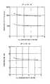
- Figs. 2 to 6are diagrams showing the results of experiments on SiO2 films formed by the CVD process of the present invention.
- Fig. 2is a diagram showing the relationship between the O3 concentration and the SiO2 film deposition rate, wherein the abscissa represents the O3 concentration (mol %) while the ordinate represents the deposition rate ( ⁇ /min).
- the temperature of the wafers (substrates)was 400 °C and the temperature of the OMCTS solution (source temperature) was 40 °C.
- the flow rate of the carrier gas N2was 4.0 SLM (standard liter/min).
- marks of white circleindicate that the underlying surface was of an Si film
- marks of black circleindicate that the underlying surface was of a thermal SiO2 film.
- the deposition ratewas substantially constant and stable when the O3 concentration was 1 mol % or more. This will prove that an O3 concentration of about 1 mol % or more can facilitate the production process control.
- the deposition rate in the process of the present inventionwas compared with that in the conventional TEOS-O3 process.
- the deposition rate in the conventional TEOS-O3 processwas 1,000 ⁇ /min, whereas the deposition rate in the OMCTS-O3 process according to the present invention was 2,2000 ⁇ /min.
- the deposition rateis at least two times as high as that in the conventional TEOS-O3 process to be able to improve the throughput.
- Fig. 3is a diagram showing the relationship between the O3 concentration (mol %) and the etching rate ( ⁇ /min) of SiO2 film formed by the CVD process of the present invention.
- marks of white circleindicate that the underlying surface was of an Si film
- marks of black circleindicate that the underlying surface was of a thermal SiO2 film.
- the etching ratewas substantially constant and stable when the O3 concentration was 1 mol % or more. This will prove that an O3 concentration of about 1 mol % or more can facilitate the control of an operation of etching an SiO2 film into a patterned film.
- Fig. 4is a diagram showing the relationship between the O3 concentration (mol %) and the shrinkage (%) of SiO2 film formed by the CVD process of the present invention.
- the shirinkagewas examined through measurement of respective film thicknesses before and after annealing (at 850 °C, for 30 sec, under N2). In this case as well, no substantial dependence of film shrinkage on O3 concentration was recognized. Furthermore, a very low level of film shrinkage will prove that the films were dense and of good quality.
- Fig. 5is a diagram showing the relationship between the O3 concentration and the stress of SiO2 film formed by the CVD process of the present invention, wherein the abscissa represents the O3 concentration (mol %) while the ordinate represents the stress (109 dyne/cm2) with time being a parameter.
- the abscissarepresents the O3 concentration (mol %)
- the ordinaterepresents the stress (109 dyne/cm2) with time being a parameter.
- marks of white circleindicate that the stress was examined immediately after film deposition
- marks of white triangleindicate that the stress was examined 24 hours after the film deposition. The stress was examined through measurement of film warping.
- the value of stress examined a while after film depositionis of more significance than that examined immediately after the film deposition.
- the dependence of stress on O3 concentrationwas low, and the stress values were on a low level.
- Fig. 6is a diagram showing an infrared absorption curve of an SiO2 film formed by the CVD process of the present invention, wherein the abscissa represents the wavenumber (cm ⁇ 1) of infrared rays while the ordinate represents the relative absorption, the absolute values of which do not have any special meaning.
- This curveis indicative of the moisture content of the SiO2 film. More specifically, the absorption at around 950 cm ⁇ 1 is assigned to OH groups constituting water molecules (H2O). The very low absorption at around 950 cm ⁇ 1 in the curve will prove that the SiO2 film had a low moisture content and was of good quality with low moisture absorption.
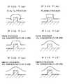
- Figs. 7 (a) to (f)compares the coverage, around a stepped portion, of an SiO2 film formed by the CVD process of the present invention with those of SiO2 films formed by conventional CVD processes.
- Such stepped portions of the underlying surfaceare formed when electrodes and wirings are formed.
- Fig. 7 (a)illustrates the coverage of an SiO2 film formed by the conventional SiH4 -O2 process, which includes constrictions around stepped portions of the underlying surface to give rise to liability to disconnection of wirings formed thereon.
- Fig. 7 (b)illustrates the coverage of an SiO2 film formed by a conventional plasma process, which includes a faithful reflection of the shapes of stepped portions of the underlying surface to give rise to a downgraded reliability of wirings formed thereon.
- Fig. 7 (c)illustrates the coverage of an SiO2 film formed at an O3 concentration of 0.6 mol % by the conventional TEOS-O3 process, which is in an isotropic deposition profile and includes a reflection of the shapes of stepped portions of the underlying surface to give rise to liability to disconnection of wirings formed thereon.
- Fig. 7 (d)illustrates the coverage of an SiO2 film deposited at an O3 concentration of 4 mol % by the conventional TEOS-O3 process, which is in a flowing profile, but involves a possibility of sometimes entailing a downgraded reliability of wirings formed thereon.
- Figs. 7 (e) and (f)illustrate the respective coverages of SiO2 films deposited at O3 concentrations of 0.6 mol % and 4 mol %, respectively, by the OMCTS-O3 process of the present invention, which are in a flowing profile and hardly give rise to disconnection of wirings formed thereon.
- an SiO2 film formed by the OMCTS-O3 process of the present inventionis always deposited in a flowing profile even around stepped portions of the underlying surface without any substantial dependence on the O3 concentration to hardly give rise to liability to disconnection of wirings formed thereon. Accordingly, the process of the present invention is very effectively applicable to production of semiconductor devices with multi-layer wirings and the like.
- the OMCTS-O3 process according to the present inventionwas used at O3 concentrations of 0.6 mol % and 4 mol % to form respective SiO2 films around grooves having an aspect ratio of 5 (width: 0.8 ⁇ m, depth: 4 ⁇ m).
- the grooveswere filled up with the respective SiO2 films without formation of voids.
- the OMCTS-O3 process according to the present inventionis advantageous in that the film growth rate is high and substantially independent of the O3 concentration as compared with conventional CVD processes, particularly the TEOS-O3 process. This will advantageously raise the productivity and facilitate the production process control.
- the reactionoccurs on the underlying surface to cause very little generation of particles. This can prevent a decrease in the yield of semiconductor devices, which would otherwise be attributable to particles, and can improve the reliability of semiconductor devices because of the high density and low moisture absorption of SiO2 films formed by the process of the present invention.
- An SiO2 film formed by the process of the present inventioncan perfectly fill up a groove having even a high aspect ratio without formation of voids, and is in such a flowing profile even around angular parts of stepped portions of the underlying surface that wirings formed thereon hardly undergo disconnection.
Landscapes
- Engineering & Computer Science (AREA)
- Chemical & Material Sciences (AREA)
- Manufacturing & Machinery (AREA)
- Condensed Matter Physics & Semiconductors (AREA)
- Power Engineering (AREA)
- Microelectronics & Electronic Packaging (AREA)
- Computer Hardware Design (AREA)
- General Physics & Mathematics (AREA)
- Physics & Mathematics (AREA)
- Chemical Kinetics & Catalysis (AREA)
- Mechanical Engineering (AREA)
- Organic Chemistry (AREA)
- Inorganic Chemistry (AREA)
- Metallurgy (AREA)
- Materials Engineering (AREA)
- General Chemical & Material Sciences (AREA)
- Formation Of Insulating Films (AREA)
- Internal Circuitry In Semiconductor Integrated Circuit Devices (AREA)
Abstract
Description
- The present invention relates to a process for forming a CVD (chemical vapor deposition) film and a semiconductor device, and more particularly to a process for forming an insulating film such as an SiO₂ film according to a CVD method and a semiconductor device using such a CVD film.
- The multi-layer wiring technology has been in progress as a powerful means for increasing the scale of integration of semiconductor devices. In keeping with this, development of a method of forming an interlayer insulating film which is most adaptable for a multi-layer wiring structure has been increasingly in demand. In order to eliminate disconnection of metallic wirings because of stress migration and minimize the strain of devices and the like because of thermal stress, there has recently been a demand for development of a process capable of forming an interlayer insulating film at as low a temperature as possible.
- Various proposals have heretofore been made of processes for forming an SiO₂ film according to a chemical vapor deposition method (hereinafter referred to as a "CVD method"), among which representative processes capable of forming an SiO₂ film at a low temperature in particular include those mentioned below.
- This is a process for depositing an SiO₂ film on a semiconductor substrate at a temperature of 350 to 450 °C according to a reaction represented by the following formula: SiH₄ + SiO₂ → SiO₂ + 2H₂. This reaction occurs in a gaseous phase, and hence an SiO₂ film is formed through simple deposition.
- Acccording to this process, a large number of particles are liable to be generated to deteriorate the quality of the resulting film and liable to give rise to uptake of moisture into the film, presenting a problem of poor reliability. Furthermore, the poor step coverage of the film entails a problem of disconnection of wirings formed on the film. Moreover, special care must be taken of SiH₄ as a reactive gas to be used in the reaction because of its self-burning properties. This makes the handling of SiH₄ complicated.
- This method is advantageous in that an SiO₂ film can be formed at a temperature as low as 300 to 400 °C. However, since it is a film formation process utilizing charged particles, damage to a device is so great that the process is unsuitable for use in production of very fine devices and VLSI structures. Furthermore, plasma discharge is so liable to break down all kinds of chemical bonds that a good-quality film can not always be obtained. Moreover, the process involves generation of a large number of particles and a great possibility that metallic atoms and the like constituting the inside of a reaction chamber used in the process may be incorporated into the resulting film to cause contamination of the film. In addition, the film obtained by the process has a problem of poor step coverage.
- This is a process wherein TEOS (tetraethyl ortho-silicate, Si(OC₂H₅)₄, an alkoxysilane) is decomposed with the aid of O₃ (ozone) to form an SiO₂ film.
- This method has various advantages such as safety of TEOS, good step coverage, little generation of particles, and other merits in association with the reaction rate determination of surface. Accordingly, this process can eliminate the defects of the above-mentioned SiH₄-O₂ process (1) and plasma CVD process using SiH₄-N₂O and the like (2).
- In accordance with the process for forming an SiO₂ film according to the TEOS-O₃ reaction, however, the deposition rate of an SiO₂ film is dependent upon the O₃ concentration, while the film quality thereof is not always satisfactory and the step coverage of the film around stepped portions of the underlying surface turns from flowing profiles into isotropic profiles as the O₃ concentration is decreased (about 3 mol % or less). This entails a difficulty in using such SiO₂ films as interlayer insulating films.
- Furthermore, when the underlying surface is of a thermal SiO₂ film, the unevenness, or roughness, of the surface of an SiO₂ film formed thereon by the TEOS-O₃ process increases with an increase in the O₃ concentration to increase the possibility of causing failures such as disconnection of wirings.
- Moreover, the TEOS-O₃ reaction involves a high possibility of particle generation because it is not necessarily a perfect surface reaction.
- Thus, in accordance with the process for forming an SiO₂ film according to the TEOS-O₃ reaction, the film quality, the step coverage, the film surface state, the film deposition rate, etc. are so dependent upon the O₃ concentration that SiO₂ films cannot always be formed stably.
- The present invention has been made in view of the foregoing problems of the prior art. Accordingly, an object of the present invention is to provide a novel CVD process easy of production control with a constant deposition rate and capable of forming a good-quality CVD film with good step coverage and other characteristics.
- In accordance with the present invention, there is provided a process for forming a CVD film, comprising reacting a polysiloxane compound having at least two silicon-oxygen bonds with ozone to form an SiO₂ film.
- Examples of the polysiloxane compound having at least two silicon-oxygen bonds include linear siloxane compounds represented by the following formula:

which include hexamethyldisiloxane. - Other examples of the polysiloxane compounds having at least two silicon-oxygen bonds include cyclic siloxane compounds represented by the following formula:

which include octamethylcyclotetrasiloxane (OMCTS) represented by the following molecular formula:
and hexamethylcyclotrisiloxane. - In the above-mentioned formulae, R stands for an alkyl group which includes no hydrophilic substituent groups such as

- When a PSG film, a BSG film or a BPSG film is to be formed by the CVD process of the present invention, the above-mentioned polysiloxane compound having at least two silicon-oxygen bonds is mixed with a gas containing an impurity such as phosphorus or boron to be reacted with ozone.
- The CVD process of the present invention has the following features:
- (1) The reaction does not occur in a gaseous phase, but mainly on the underlying surface. This results in very little generation of particles. Additionally stated, although film deposition occurs on a heater, a susceptor, etc., the deposited films are very dense not in a flaky form to fail as particle generation sources.
- (2) Good-quality films having the following properties can be obtained stably without any dependence on the O₃ concentration.
- (a) The moisture content of the films is low with little moisture absorption.
- (b) The insulating properties of the films are good with little leak current.
- (c) The shrinkage of the films is low with low tensile stress.
- (d) The etching rate of the films is constant.
- (3) The step coverages of the films are in a flowing profile and any deep grooves can be filled up with the films without formation of voids. This is an advantage over any conventional processes.
- (4) The film deposition rate can be raised as compared with that in the case of the conventional TEOS-O₃ process (TEOS includes one Si-O bond in one molecule thereof.) because the polysiloxane compound to be used in the present invention includes at least two Si-O bonds in one molecule thereof.
- The foregoing and other objects, features and advantages of the present invention will be better understood from the following description taken in connection with the accomapnying drawings, in which:
- Fig. 1 is a schematic illustration of production equipment for use in a CVD process in Example according to the present invention;
- Fig. 2 is a diagram showing a variation of deposition rate with ozone concentration;
- Fig. 3 is a diagram showing a variation of etching rate of SiO₂ film with ozone concentration;
- Fig. 4 is a diagram showing a variation of shrinkage of SiO₂ film with ozone concentration;
- Fig. 5 is a diagram showing a variation of stress of SiO₂ with ozone concentration;
- Fig. 6 is a diagram showing an infrared absorption curve indicative of the OH group content of an SiO₂; and
- Fig. 7 is an illustration comparing the step coverage of an SiO₂ film formed according to the process of the present invention with those of SiO₂ films formed according to conventional processes.
- Fig. 1 is a schematic illustration of production equipment for use in the CVD process of Example according to the present invention, which will be given later.
- The equipment of Fig. 1 comprises mass flow controllers (MFC) 2a to 2d,
valves 4b to 4h, anozone generator 6 wherein oxygen (O₂) is converted into ozone (O₃), aresorvoir 8 wherein a solution of OMCTS (octamethylcyclotetrasiloxane) is kept at a temperature of about 40 to 65 °C, aresorvoir 10 wherein a solution of TMPO (trimethyl phosphate) is kept at a temperature of about 50 to 60 °C, aresorvoir 12 wherein a solution of TEB (triethyl borate) is kept at a temperature of about 5 to 50 °C, and aCVD chamber 14. - The
chamber 14 includes aheater 16, agas outflow head 18, and agas discharge outlet 20. Wafers 22a and 22b as substrates for film formation thereon is in place in thechamber 14. - The procedure of forming an SiO₂ film using the equipment of Fig. 1 is as follows. The
valves 4a to 4d are opened. This entails generation of O₃ gas in theozone generator 6, from which the O₃ gas is fed into thechamber 14 through thegas inflow head 18, through which OMCTS gas on a carrier gas N₂ is also fed into thechamber 14. The ensuing OMCTS-O₃ reaction forms SiO₂ films on thewafers - When PGS films are to be formed, the
valves 4a to 4f are opened. This entails feeding, into thechamber 14, of O₃ gas as well as OMCTS and TMPO gases on a carrier gas N₂. The ensuing OMCTS-TMPO-O₃ reaction forms PSG films on thewafers - When BSG films are to be formed, the
valves 4a to 4d, 4g and 4h are opened. This entails feeding, into thechamber 14, of O₃ gas as well as OMCTS and TEB gases on a carrier gas N₂. The ensuing OMCTS-TEB-O₃ reaction forms BSG films on thewafers - When BPSG films are to be formed, the
valves 4a to 4h are opened. This entails feeding, into thechamber 14, of O₃ gas as well as OMCTS, TMPO and TEB gases on a carrier gas N₂. The ensuing OMCTS-TMPO-TEB-O₃ reaction forms BPSG films on thewafers - Example according to the present invention will now be described while referring to the accompanying drawings.
- Figs. 2 to 6 are diagrams showing the results of experiments on SiO₂ films formed by the CVD process of the present invention.
- Fig. 2 is a diagram showing the relationship between the O₃ concentration and the SiO₂ film deposition rate, wherein the abscissa represents the O₃ concentration (mol %) while the ordinate represents the deposition rate (Å/min). The temperature of the wafers (substrates) was 400 °C and the temperature of the OMCTS solution (source temperature) was 40 °C. The flow rate of the carrier gas N₂ was 4.0 SLM (standard liter/min).
- In the figure, marks of white circle indicate that the underlying surface was of an Si film, while marks of black circle indicate that the underlying surface was of a thermal SiO₂ film. In either case, the deposition rate was substantially constant and stable when the O₃ concentration was 1 mol % or more. This will prove that an O₃ concentration of about 1 mol % or more can facilitate the production process control.
- Under the same process conditions, the deposition rate in the process of the present invention was compared with that in the conventional TEOS-O₃ process.
- (a) substrate temperature: 400 °C
- (b) source temperature: 65 °C (saturated vapor pressure: 20 mmHg)
- (c) O₃ concentration: 40,000 ppm (by mol)
- (d) flow rate of carrier gas N₂: 3.5 SLM
- Under the above-mentioned conditions, the deposition rate in the conventional TEOS-O₃ process was 1,000 Å/min, whereas the deposition rate in the OMCTS-O₃ process according to the present invention was 2,2000 Å/min.
- Thus, according to the present invention, the deposition rate is at least two times as high as that in the conventional TEOS-O₃ process to be able to improve the throughput.
- Fig. 3 is a diagram showing the relationship between the O₃ concentration (mol %) and the etching rate (Å/min) of SiO₂ film formed by the CVD process of the present invention.
- In the figure, marks of white circle indicate that the underlying surface was of an Si film, while marks of black circle indicate that the underlying surface was of a thermal SiO₂ film. In either case, the etching rate was substantially constant and stable when the O₃ concentration was 1 mol % or more. This will prove that an O₃ concentration of about 1 mol % or more can facilitate the control of an operation of etching an SiO₂ film into a patterned film.
- Fig. 4 is a diagram showing the relationship between the O₃ concentration (mol %) and the shrinkage (%) of SiO₂ film formed by the CVD process of the present invention. The shirinkage was examined through measurement of respective film thicknesses before and after annealing (at 850 °C, for 30 sec, under N₂). In this case as well, no substantial dependence of film shrinkage on O₃ concentration was recognized. Furthermore, a very low level of film shrinkage will prove that the films were dense and of good quality.
- Fig. 5 is a diagram showing the relationship between the O₃ concentration and the stress of SiO₂ film formed by the CVD process of the present invention, wherein the abscissa represents the O₃ concentration (mol %) while the ordinate represents the stress (10⁹ dyne/cm²) with time being a parameter. In the figure, marks of white circle indicate that the stress was examined immediately after film deposition, while marks of white triangle indicate that the stress was examined 24 hours after the film deposition. The stress was examined through measurement of film warping.
- In actual wafer processing, the value of stress examined a while after film deposition is of more significance than that examined immediately after the film deposition. In this case as well, the dependence of stress on O₃ concentration was low, and the stress values were on a low level.
- Fig. 6 is a diagram showing an infrared absorption curve of an SiO₂ film formed by the CVD process of the present invention, wherein the abscissa represents the wavenumber (cm⁻¹) of infrared rays while the ordinate represents the relative absorption, the absolute values of which do not have any special meaning.
- This curve is indicative of the moisture content of the SiO₂ film. More specifically, the absorption at around 950 cm⁻¹ is assigned to OH groups constituting water molecules (H₂O). The very low absorption at around 950 cm⁻¹ in the curve will prove that the SiO₂ film had a low moisture content and was of good quality with low moisture absorption.
- Figs. 7 (a) to (f) compares the coverage, around a stepped portion, of an SiO₂ film formed by the CVD process of the present invention with those of SiO₂ films formed by conventional CVD processes. Such stepped portions of the underlying surface are formed when electrodes and wirings are formed.
- Fig. 7 (a) illustrates the coverage of an SiO₂ film formed by the conventional SiH₄ -O₂ process, which includes constrictions around stepped portions of the underlying surface to give rise to liability to disconnection of wirings formed thereon. Fig. 7 (b) illustrates the coverage of an SiO₂ film formed by a conventional plasma process, which includes a faithful reflection of the shapes of stepped portions of the underlying surface to give rise to a downgraded reliability of wirings formed thereon.
- Fig. 7 (c) illustrates the coverage of an SiO₂ film formed at an O₃ concentration of 0.6 mol % by the conventional TEOS-O₃ process, which is in an isotropic deposition profile and includes a reflection of the shapes of stepped portions of the underlying surface to give rise to liability to disconnection of wirings formed thereon.
- Fig. 7 (d) illustrates the coverage of an SiO₂ film deposited at an O₃ concentration of 4 mol % by the conventional TEOS-O₃ process, which is in a flowing profile, but involves a possibility of sometimes entailing a downgraded reliability of wirings formed thereon.
- Figs. 7 (e) and (f) illustrate the respective coverages of SiO₂ films deposited at O₃ concentrations of 0.6 mol % and 4 mol %, respectively, by the OMCTS-O₃ process of the present invention, which are in a flowing profile and hardly give rise to disconnection of wirings formed thereon.
- As is apparent from the foregoing description, an SiO₂ film formed by the OMCTS-O₃ process of the present invention is always deposited in a flowing profile even around stepped portions of the underlying surface without any substantial dependence on the O₃ concentration to hardly give rise to liability to disconnection of wirings formed thereon. Accordingly, the process of the present invention is very effectively applicable to production of semiconductor devices with multi-layer wirings and the like.
- The OMCTS-O₃ process according to the present invention was used at O₃ concentrations of 0.6 mol % and 4 mol % to form respective SiO₂ films around grooves having an aspect ratio of 5 (width: 0.8 µm, depth: 4 µm). The grooves were filled up with the respective SiO₂ films without formation of voids.
- As described hereinbefore, the OMCTS-O₃ process according to the present invention is advantageous in that the film growth rate is high and substantially independent of the O₃ concentration as compared with conventional CVD processes, particularly the TEOS-O₃ process. This will advantageously raise the productivity and facilitate the production process control.
- Furthermore, according to the present invention, the reaction occurs on the underlying surface to cause very little generation of particles. This can prevent a decrease in the yield of semiconductor devices, which would otherwise be attributable to particles, and can improve the reliability of semiconductor devices because of the high density and low moisture absorption of SiO₂ films formed by the process of the present invention.
- An SiO₂ film formed by the process of the present invention can perfectly fill up a groove having even a high aspect ratio without formation of voids, and is in such a flowing profile even around angular parts of stepped portions of the underlying surface that wirings formed thereon hardly undergo disconnection.
- Accordingly, when the CVD process of the present invention is used to form interlayer insulating films and the like, semiconductor devices with a highly reliable multi-layer wiring structure can be produced.


Claims (4)
- A process for forming a CVD film, comprising reacting a polysiloxane compound having at least two silicon-oxygen bonds with ozone to form an SiO₂ film.
- A process for forming a CVD film as claimed in claim 1, wherein said reaction of said polysiloxane compound having at least two silicon-oxygen bonds with ozone is effected in the presence of a gas mixed therewith and containing an impurity such as phosphorus or boron to form a PSG, BSG, BPSG or like film.
- A process for forming a CVD film as claimed in claim 1 or 2, wherein said polysiloxane compound having at least two silicon-oxygen bonds is a member selected from the group consisting of linear siloxane compounds represented by the following formula:


- A semiconductor device comprising an SiO₂ film as set forth in claim, or a PSG, BSG, BPSG or like film as set forth in claim 2, which is formed as a planarizing film, an interlayer insulating film, or a cover insulating film.


Applications Claiming Priority (2)
| Application Number | Priority Date | Filing Date | Title |
|---|---|---|---|
| JP1339071AJPH03198338A (en) | 1989-12-27 | 1989-12-27 | Vapor-phase growth film formation method and semiconductor device |
| JP339071/89 | 1989-12-27 |
Publications (2)
| Publication Number | Publication Date |
|---|---|
| EP0436185A1true EP0436185A1 (en) | 1991-07-10 |
| EP0436185B1 EP0436185B1 (en) | 1996-03-20 |
Family
ID=18323985
Family Applications (1)
| Application Number | Title | Priority Date | Filing Date |
|---|---|---|---|
| EP90124838AExpired - LifetimeEP0436185B1 (en) | 1989-12-27 | 1990-12-19 | Process for forming SiO2 film with polysiloxane/ozone reaction |
Country Status (4)
| Country | Link |
|---|---|
| US (1) | US5231058A (en) |
| EP (1) | EP0436185B1 (en) |
| JP (1) | JPH03198338A (en) |
| DE (1) | DE69026059T2 (en) |
Cited By (9)
| Publication number | Priority date | Publication date | Assignee | Title |
|---|---|---|---|---|
| EP0497541A1 (en)* | 1991-01-28 | 1992-08-05 | Kawasaki Steel Corporation | Semiconductor device with a borophosphosilicate glass and method of manufacturing the same |
| EP0471139A3 (en)* | 1990-08-16 | 1993-01-07 | Corning Incorporated | Method of making high purity, non-porous fused silica bodies |
| EP0525984A1 (en)* | 1991-06-29 | 1993-02-03 | Shin-Etsu Quartz Products Co., Ltd. | Method for manufacturing a silica glass article for use with an excimer laser |
| EP0470632A3 (en)* | 1990-08-10 | 1993-04-21 | Semiconductor Process Laboratory Co., Ltd. | Method of manufacturing a silicon oxide film and an oxide based glass for semiconductor devices |
| EP0575650A1 (en)* | 1992-06-22 | 1993-12-29 | Semiconductor Process Laboratory Co., Ltd. | Method of reforming an insulating film in a semiconductor device and apparatus therefor |
| EP0481777A3 (en)* | 1990-10-17 | 1994-08-17 | Semiconductor Energy Lab | Method of manufacturing gate insulated field effect transistors |
| US5376591A (en)* | 1992-06-05 | 1994-12-27 | Semiconductor Process Laboratory Co., Ltd. | Method for manufacturing semiconductor device |
| EP0736905A3 (en)* | 1993-08-05 | 1998-04-22 | Matsushita Electronics Corporation | Semiconductor device having capacitor and manufacturing method thereof |
| EP1204987A4 (en)* | 1999-07-09 | 2002-10-30 | Asml Us Inc | CHEMICAL VAPOR DEPOSITION OF SILICON OXIDE FILMS USING ALKYLSILOXANE OLIGOMERS WITH OZONE |
Families Citing this family (19)
| Publication number | Priority date | Publication date | Assignee | Title |
|---|---|---|---|---|
| DE4202652C2 (en)* | 1992-01-30 | 1996-03-28 | Fraunhofer Ges Forschung | Process for applying a UV and / or electron beam sensitive lacquer layer |
| EP0582724A1 (en)* | 1992-08-04 | 1994-02-16 | Siemens Aktiengesellschaft | Method of CVD deposition of SiO2 layers with local and global planarization on structured silicon substrates |
| US5489553A (en)* | 1995-05-25 | 1996-02-06 | Industrial Technology Research Institute | HF vapor surface treatment for the 03 teos gap filling deposition |
| US6489255B1 (en)* | 1995-06-05 | 2002-12-03 | International Business Machines Corporation | Low temperature/low dopant oxide glass film |
| US6489213B1 (en) | 1996-01-05 | 2002-12-03 | Integrated Device Technology, Inc. | Method for manufacturing semiconductor device containing a silicon-rich layer |
| WO1997028561A1 (en)* | 1996-02-02 | 1997-08-07 | Micron Technology, Inc. | Reducing fixed charge in semiconductor device layers |
| US5710079A (en)* | 1996-05-24 | 1998-01-20 | Lsi Logic Corporation | Method and apparatus for forming dielectric films |
| US6013583A (en)* | 1996-06-25 | 2000-01-11 | International Business Machines Corporation | Low temperature BPSG deposition process |
| US5990513A (en) | 1996-10-08 | 1999-11-23 | Ramtron International Corporation | Yield enhancement technique for integrated circuit processing to reduce effects of undesired dielectric moisture retention and subsequent hydrogen out-diffusion |
| WO1998015499A1 (en)* | 1996-10-08 | 1998-04-16 | Corning Incorporated | Method of inhibiting gelling of siloxane feedstocks and a gel inhibited feedstock |
| US6159870A (en)* | 1998-12-11 | 2000-12-12 | International Business Machines Corporation | Borophosphosilicate glass incorporated with fluorine for low thermal budget gap fill |
| US6165905A (en)* | 1999-01-20 | 2000-12-26 | Philips Electronics, North America Corp. | Methods for making reliable via structures having hydrophobic inner wall surfaces |
| US6242299B1 (en) | 1999-04-01 | 2001-06-05 | Ramtron International Corporation | Barrier layer to protect a ferroelectric capacitor after contact has been made to the capacitor electrode |
| EP1123991A3 (en)* | 2000-02-08 | 2002-11-13 | Asm Japan K.K. | Low dielectric constant materials and processes |
| US6905981B1 (en) | 2000-11-24 | 2005-06-14 | Asm Japan K.K. | Low-k dielectric materials and processes |
| US6572923B2 (en)* | 2001-01-12 | 2003-06-03 | The Boc Group, Inc. | Asymmetric organocyclosiloxanes and their use for making organosilicon polymer low-k dielectric film |
| US8723654B2 (en) | 2010-07-09 | 2014-05-13 | Cypress Semiconductor Corporation | Interrupt generation and acknowledgment for RFID |
| US9846664B2 (en) | 2010-07-09 | 2017-12-19 | Cypress Semiconductor Corporation | RFID interface and interrupt |
| US9092582B2 (en) | 2010-07-09 | 2015-07-28 | Cypress Semiconductor Corporation | Low power, low pin count interface for an RFID transponder |
Citations (3)
| Publication number | Priority date | Publication date | Assignee | Title |
|---|---|---|---|---|
| US4168330A (en)* | 1977-10-13 | 1979-09-18 | Rca Corporation | Method of depositing a silicon oxide layer |
| EP0286097A2 (en)* | 1987-04-10 | 1988-10-12 | Air Products And Chemicals, Inc. | Method of forming silicon dioxide glass films |
| EP0367004A1 (en)* | 1988-10-26 | 1990-05-09 | Texas Instruments Incorporated | Deposition of silicon-containing films using organosilicon compounds and nitrogen trifluoride |
Family Cites Families (5)
| Publication number | Priority date | Publication date | Assignee | Title |
|---|---|---|---|---|
| US5028566A (en)* | 1987-04-10 | 1991-07-02 | Air Products And Chemicals, Inc. | Method of forming silicon dioxide glass films |
| JP2624254B2 (en)* | 1987-05-22 | 1997-06-25 | 東京応化工業株式会社 | Method for improving film quality of silica-based coating |
| JPH0682650B2 (en)* | 1987-06-10 | 1994-10-19 | 東京エレクトロン株式会社 | Oxide film formation method |
| JPH07120734B2 (en)* | 1987-09-25 | 1995-12-20 | 日本電気株式会社 | Method for manufacturing semiconductor device |
| JPH01212442A (en)* | 1988-02-19 | 1989-08-25 | Fujitsu Ltd | Vapor growth method |
- 1989
- 1989-12-27JPJP1339071Apatent/JPH03198338A/enactivePending
- 1990
- 1990-12-14USUS07/628,237patent/US5231058A/ennot_activeExpired - Fee Related
- 1990-12-19EPEP90124838Apatent/EP0436185B1/ennot_activeExpired - Lifetime
- 1990-12-19DEDE69026059Tpatent/DE69026059T2/ennot_activeExpired - Fee Related
Patent Citations (3)
| Publication number | Priority date | Publication date | Assignee | Title |
|---|---|---|---|---|
| US4168330A (en)* | 1977-10-13 | 1979-09-18 | Rca Corporation | Method of depositing a silicon oxide layer |
| EP0286097A2 (en)* | 1987-04-10 | 1988-10-12 | Air Products And Chemicals, Inc. | Method of forming silicon dioxide glass films |
| EP0367004A1 (en)* | 1988-10-26 | 1990-05-09 | Texas Instruments Incorporated | Deposition of silicon-containing films using organosilicon compounds and nitrogen trifluoride |
Non-Patent Citations (4)
| Title |
|---|
| EXTENDED ABSTRACTS OF THE 1988 FALL MEETING, CHICAGO, ILLINOIS vol. 88-2, 09 October 1988, Princeton, NEW JERSEY pages 335 - 336; A.K. HOCHBERG et al.: "Silicon oxide deposition from cyclic siloxane precursors"* |
| EXTENDED ABSTRACTS OF THE 19th. CONFERENCE ON SOLID STATE DEVICES AND MATERIALS, TOKYO 25 August 1987, pages 447 - 450; Y. NISHIMOTO et al.: "Low temperature chemical vapor deposition of dielectric films using ozone and organosilane"* |
| NEC RESEARCH AND DEVELOPMENT. no. 94, July 1989, TOKYO JP pages 1 - 7; Yasuo IKEDA et al.: "Ozone/organic-source APCVD for ULSI reflow glass films"* |
| PROCEEDINGS OF THE 1989 VMIC CONFERENCE 12 June 1989, pages 382 - 389; Y. NISHIMOTO et al.: "Dielectric film deposition by atmospheric pressure and low temperature CVD using TEOS, ozone and new organometallic doping sources"* |
Cited By (12)
| Publication number | Priority date | Publication date | Assignee | Title |
|---|---|---|---|---|
| EP0470632A3 (en)* | 1990-08-10 | 1993-04-21 | Semiconductor Process Laboratory Co., Ltd. | Method of manufacturing a silicon oxide film and an oxide based glass for semiconductor devices |
| US5484749A (en)* | 1990-08-10 | 1996-01-16 | Alcan-Tech Co., Inc. | Manufacturing method of semiconductor device |
| EP0471139A3 (en)* | 1990-08-16 | 1993-01-07 | Corning Incorporated | Method of making high purity, non-porous fused silica bodies |
| EP0481777A3 (en)* | 1990-10-17 | 1994-08-17 | Semiconductor Energy Lab | Method of manufacturing gate insulated field effect transistors |
| EP0497541A1 (en)* | 1991-01-28 | 1992-08-05 | Kawasaki Steel Corporation | Semiconductor device with a borophosphosilicate glass and method of manufacturing the same |
| US5336640A (en)* | 1991-01-28 | 1994-08-09 | Kawasaki Steel Corporation | Method of manufacturing a semiconductor device having an insulating layer composed of a BPSG film and a plasma-CVD silicon nitride film |
| EP0525984A1 (en)* | 1991-06-29 | 1993-02-03 | Shin-Etsu Quartz Products Co., Ltd. | Method for manufacturing a silica glass article for use with an excimer laser |
| US5376591A (en)* | 1992-06-05 | 1994-12-27 | Semiconductor Process Laboratory Co., Ltd. | Method for manufacturing semiconductor device |
| EP0575650A1 (en)* | 1992-06-22 | 1993-12-29 | Semiconductor Process Laboratory Co., Ltd. | Method of reforming an insulating film in a semiconductor device and apparatus therefor |
| US5387546A (en)* | 1992-06-22 | 1995-02-07 | Canon Sales Co., Inc. | Method for manufacturing a semiconductor device |
| EP0736905A3 (en)* | 1993-08-05 | 1998-04-22 | Matsushita Electronics Corporation | Semiconductor device having capacitor and manufacturing method thereof |
| EP1204987A4 (en)* | 1999-07-09 | 2002-10-30 | Asml Us Inc | CHEMICAL VAPOR DEPOSITION OF SILICON OXIDE FILMS USING ALKYLSILOXANE OLIGOMERS WITH OZONE |
Also Published As
| Publication number | Publication date |
|---|---|
| JPH03198338A (en) | 1991-08-29 |
| DE69026059T2 (en) | 1996-08-22 |
| DE69026059D1 (en) | 1996-04-25 |
| EP0436185B1 (en) | 1996-03-20 |
| US5231058A (en) | 1993-07-27 |
Similar Documents
| Publication | Publication Date | Title |
|---|---|---|
| EP0436185B1 (en) | Process for forming SiO2 film with polysiloxane/ozone reaction | |
| US5288518A (en) | Chemical vapor deposition method for forming fluorine containing silicon oxide film | |
| US5314724A (en) | Process for forming silicon oxide film | |
| US5840631A (en) | Method of manufacturing semiconductor device | |
| US5166101A (en) | Method for forming a boron phosphorus silicate glass composite layer on a semiconductor wafer | |
| US5028566A (en) | Method of forming silicon dioxide glass films | |
| US5484749A (en) | Manufacturing method of semiconductor device | |
| EP0478308A2 (en) | Method of forming interlayer-insulating film | |
| US5250473A (en) | Method of providing silicon dioxide layer on a substrate by means of chemical reaction from the vapor phase at a low pressure (LPCVD) | |
| EP0421203B1 (en) | An integrated circuit structure with a boron phosphorus silicate glass composite layer on semiconductor wafer and improved method for forming same | |
| JP3532830B2 (en) | Semiconductor device and manufacturing method thereof | |
| US5324539A (en) | Method for forming CVD thin glass films | |
| JP4032044B2 (en) | Film forming method, semiconductor device manufacturing method, and semiconductor device | |
| Barron | CVD of SiO2 and related materials: An overview | |
| EP0481706B1 (en) | Method of producing CVD silicon oxynitride film | |
| US5061514A (en) | Chemical vapor deposition (CVD) process for plasma depositing silicon carbide films onto a substrate | |
| US5053255A (en) | Chemical vapor deposition (CVD) process for the thermally depositing silicon carbide films onto a substrate | |
| KR100339820B1 (en) | Film formation method and manufacturing method semiconductor device | |
| US8420170B2 (en) | Methods of forming glass on a substrate | |
| US6432839B2 (en) | Film forming method and manufacturing method of semiconductor device | |
| KR100200888B1 (en) | Method of forming an inter-layer insulating film | |
| JPH06283519A (en) | Manufacture of semiconductor device | |
| JP3070894B2 (en) | Thin film formation method | |
| Zanotti et al. | Process characterization for LPCVD TEOS-ozone based SiO2 films | |
| Dorrance et al. | Unique very low temperature plasma‐enhanced chemical‐vapor deposition glass process for hot and cold wall commercial reactors |
Legal Events
| Date | Code | Title | Description |
|---|---|---|---|
| PUAI | Public reference made under article 153(3) epc to a published international application that has entered the european phase | Free format text:ORIGINAL CODE: 0009012 | |
| AK | Designated contracting states | Kind code of ref document:A1 Designated state(s):DE FR GB | |
| 17P | Request for examination filed | Effective date:19910910 | |
| RIN1 | Information on inventor provided before grant (corrected) | Inventor name:NISHIMOTO, YUKO, C/O SEMICONDUCTOR PROCESS Inventor name:TOKUMASU, NOBORU, C/O SEMICONDUCTOR PROCESS Inventor name:MAEDA, KAZUO, C/O SEMICONDUCTO PROCESS | |
| 17Q | First examination report despatched | Effective date:19931122 | |
| RAP1 | Party data changed (applicant data changed or rights of an application transferred) | Owner name:CANON SALES CO., INC. Owner name:ALCAN- TECH CO., INC. Owner name:SEMICONDUCTOR PROCESS LABORATORY CO., LTD. | |
| GRAH | Despatch of communication of intention to grant a patent | Free format text:ORIGINAL CODE: EPIDOS IGRA | |
| GRAA | (expected) grant | Free format text:ORIGINAL CODE: 0009210 | |
| AK | Designated contracting states | Kind code of ref document:B1 Designated state(s):DE FR GB | |
| REF | Corresponds to: | Ref document number:69026059 Country of ref document:DE Date of ref document:19960425 | |
| ET | Fr: translation filed | ||
| PLBE | No opposition filed within time limit | Free format text:ORIGINAL CODE: 0009261 | |
| STAA | Information on the status of an ep patent application or granted ep patent | Free format text:STATUS: NO OPPOSITION FILED WITHIN TIME LIMIT | |
| 26N | No opposition filed | ||
| REG | Reference to a national code | Ref country code:GB Ref legal event code:IF02 | |
| PGFP | Annual fee paid to national office [announced via postgrant information from national office to epo] | Ref country code:GB Payment date:20031126 Year of fee payment:14 | |
| PGFP | Annual fee paid to national office [announced via postgrant information from national office to epo] | Ref country code:DE Payment date:20031205 Year of fee payment:14 | |
| PGFP | Annual fee paid to national office [announced via postgrant information from national office to epo] | Ref country code:FR Payment date:20031209 Year of fee payment:14 | |
| PG25 | Lapsed in a contracting state [announced via postgrant information from national office to epo] | Ref country code:GB Free format text:LAPSE BECAUSE OF NON-PAYMENT OF DUE FEES Effective date:20041219 | |
| PG25 | Lapsed in a contracting state [announced via postgrant information from national office to epo] | Ref country code:DE Free format text:LAPSE BECAUSE OF NON-PAYMENT OF DUE FEES Effective date:20050701 | |
| GBPC | Gb: european patent ceased through non-payment of renewal fee | Effective date:20041219 | |
| PG25 | Lapsed in a contracting state [announced via postgrant information from national office to epo] | Ref country code:FR Free format text:LAPSE BECAUSE OF NON-PAYMENT OF DUE FEES Effective date:20050831 | |
| REG | Reference to a national code | Ref country code:FR Ref legal event code:ST |