EP0422243B1 - Method of forming polycrystalline film by chemical vapor deposition - Google Patents
Method of forming polycrystalline film by chemical vapor depositionDownload PDFInfo
- Publication number
- EP0422243B1 EP0422243B1EP90905659AEP90905659AEP0422243B1EP 0422243 B1EP0422243 B1EP 0422243B1EP 90905659 AEP90905659 AEP 90905659AEP 90905659 AEP90905659 AEP 90905659AEP 0422243 B1EP0422243 B1EP 0422243B1
- Authority
- EP
- European Patent Office
- Prior art keywords
- film
- film forming
- substrate
- gas
- active species
- Prior art date
- Legal status (The legal status is an assumption and is not a legal conclusion. Google has not performed a legal analysis and makes no representation as to the accuracy of the status listed.)
- Expired - Lifetime
Links
- 238000000034methodMethods0.000titleclaimsabstractdescription74
- 238000005229chemical vapour depositionMethods0.000titleabstractdescription11
- 239000007789gasSubstances0.000claimsabstractdescription156
- UFHFLCQGNIYNRP-UHFFFAOYSA-NHydrogenChemical compound[H][H]UFHFLCQGNIYNRP-UHFFFAOYSA-N0.000claimsabstractdescription36
- 238000009826distributionMethods0.000claimsabstractdescription5
- 239000000758substrateSubstances0.000claimsdescription144
- 230000003213activating effectEffects0.000claimsdescription74
- 239000002994raw materialSubstances0.000claimsdescription70
- 230000015572biosynthetic processEffects0.000claimsdescription43
- 239000002243precursorSubstances0.000claimsdescription17
- 230000008569processEffects0.000claimsdescription13
- 230000000737periodic effectEffects0.000claimsdescription4
- 230000003247decreasing effectEffects0.000claimsdescription3
- 239000011261inert gasSubstances0.000claimsdescription3
- 230000004913activationEffects0.000abstractdescription18
- 239000010408filmSubstances0.000description405
- 238000002474experimental methodMethods0.000description51
- 239000013078crystalSubstances0.000description42
- 238000000151depositionMethods0.000description30
- 239000000523sampleSubstances0.000description29
- 230000008021depositionEffects0.000description28
- 239000011521glassSubstances0.000description26
- 238000005530etchingMethods0.000description24
- 150000001875compoundsChemical class0.000description21
- 230000037230mobilityEffects0.000description19
- 229910004014SiF4Inorganic materials0.000description18
- 238000002441X-ray diffractionMethods0.000description18
- ABTOQLMXBSRXSM-UHFFFAOYSA-Nsilicon tetrafluorideChemical compoundF[Si](F)(F)FABTOQLMXBSRXSM-UHFFFAOYSA-N0.000description18
- 238000001228spectrumMethods0.000description16
- 230000009471actionEffects0.000description15
- 239000004065semiconductorSubstances0.000description15
- 238000006243chemical reactionMethods0.000description13
- 230000008859changeEffects0.000description11
- 239000010453quartzSubstances0.000description11
- VYPSYNLAJGMNEJ-UHFFFAOYSA-Nsilicon dioxideInorganic materialsO=[Si]=OVYPSYNLAJGMNEJ-UHFFFAOYSA-N0.000description11
- 239000001257hydrogenSubstances0.000description10
- 229910052739hydrogenInorganic materials0.000description10
- 239000000470constituentSubstances0.000description9
- 238000005268plasma chemical vapour depositionMethods0.000description8
- 239000010935stainless steelSubstances0.000description8
- 229910001220stainless steelInorganic materials0.000description8
- 229910004205SiNXInorganic materials0.000description7
- 239000012535impuritySubstances0.000description7
- 229910021420polycrystalline siliconInorganic materials0.000description7
- SBIBMFFZSBJNJF-UHFFFAOYSA-Nselenium;zincChemical compound[Se]=[Zn]SBIBMFFZSBJNJF-UHFFFAOYSA-N0.000description7
- -1silicon halideChemical class0.000description7
- HQWPLXHWEZZGKY-UHFFFAOYSA-NdiethylzincChemical compoundCC[Zn]CCHQWPLXHWEZZGKY-UHFFFAOYSA-N0.000description6
- ALCDAWARCQFJBA-UHFFFAOYSA-NethylselanylethaneChemical compoundCC[Se]CCALCDAWARCQFJBA-UHFFFAOYSA-N0.000description6
- 239000011148porous materialSubstances0.000description6
- 230000001105regulatory effectEffects0.000description6
- 229910052736halogenInorganic materials0.000description5
- 150000002366halogen compoundsChemical class0.000description5
- 150000002367halogensChemical class0.000description5
- 238000005259measurementMethods0.000description5
- MGNHOGAVECORPT-UHFFFAOYSA-NdifluorosiliconChemical compoundF[Si]FMGNHOGAVECORPT-UHFFFAOYSA-N0.000description4
- RVIXKDRPFPUUOO-UHFFFAOYSA-NdimethylselenideChemical compoundC[Se]CRVIXKDRPFPUUOO-UHFFFAOYSA-N0.000description4
- 230000001747exhibiting effectEffects0.000description4
- 230000009467reductionEffects0.000description4
- 238000011144upstream manufacturingMethods0.000description4
- 229910004016SiF2Inorganic materials0.000description3
- 239000012159carrier gasSubstances0.000description3
- 230000001276controlling effectEffects0.000description3
- 230000012010growthEffects0.000description3
- 238000010438heat treatmentMethods0.000description3
- 150000002500ionsChemical class0.000description3
- 229920005591polysiliconPolymers0.000description3
- 229910052710siliconInorganic materials0.000description3
- 229910052721tungstenInorganic materials0.000description3
- XKRFYHLGVUSROY-UHFFFAOYSA-NArgonChemical compound[Ar]XKRFYHLGVUSROY-UHFFFAOYSA-N0.000description2
- BLRPTPMANUNPDV-UHFFFAOYSA-NSilaneChemical compound[SiH4]BLRPTPMANUNPDV-UHFFFAOYSA-N0.000description2
- FAPWRFPIFSIZLT-UHFFFAOYSA-MSodium chlorideChemical compound[Na+].[Cl-]FAPWRFPIFSIZLT-UHFFFAOYSA-M0.000description2
- RBFQJDQYXXHULB-UHFFFAOYSA-NarsaneChemical compound[AsH3]RBFQJDQYXXHULB-UHFFFAOYSA-N0.000description2
- 230000005587bubblingEffects0.000description2
- VQNPSCRXHSIJTH-UHFFFAOYSA-Ncadmium(2+);carbanideChemical compound[CH3-].[CH3-].[Cd+2]VQNPSCRXHSIJTH-UHFFFAOYSA-N0.000description2
- UJYLYGDHTIVYRI-UHFFFAOYSA-Ncadmium(2+);ethaneChemical compound[Cd+2].[CH2-]C.[CH2-]CUJYLYGDHTIVYRI-UHFFFAOYSA-N0.000description2
- 239000000919ceramicSubstances0.000description2
- 238000005520cutting processMethods0.000description2
- 230000007547defectEffects0.000description2
- 238000001514detection methodMethods0.000description2
- AXAZMDOAUQTMOW-UHFFFAOYSA-NdimethylzincChemical compoundC[Zn]CAXAZMDOAUQTMOW-UHFFFAOYSA-N0.000description2
- 238000007733ion platingMethods0.000description2
- 239000000463materialSubstances0.000description2
- 239000013307optical fiberSubstances0.000description2
- 238000000206photolithographyMethods0.000description2
- 238000005546reactive sputteringMethods0.000description2
- 229910000058selaneInorganic materials0.000description2
- 239000010703siliconSubstances0.000description2
- 229920006268silicone filmPolymers0.000description2
- QTQRGDBFHFYIBH-UHFFFAOYSA-Ntert-butylarsenicChemical compoundCC(C)(C)[As]QTQRGDBFHFYIBH-UHFFFAOYSA-N0.000description2
- ZGNPLWZYVAFUNZ-UHFFFAOYSA-Ntert-butylphosphaneChemical compoundCC(C)(C)PZGNPLWZYVAFUNZ-UHFFFAOYSA-N0.000description2
- 238000002230thermal chemical vapour depositionMethods0.000description2
- VOITXYVAKOUIBA-UHFFFAOYSA-NtriethylaluminiumChemical compoundCC[Al](CC)CCVOITXYVAKOUIBA-UHFFFAOYSA-N0.000description2
- RGGPNXQUMRMPRA-UHFFFAOYSA-NtriethylgalliumChemical compoundCC[Ga](CC)CCRGGPNXQUMRMPRA-UHFFFAOYSA-N0.000description2
- OTRPZROOJRIMKW-UHFFFAOYSA-NtriethylindiganeChemical compoundCC[In](CC)CCOTRPZROOJRIMKW-UHFFFAOYSA-N0.000description2
- MCULRUJILOGHCJ-UHFFFAOYSA-NtriisobutylaluminiumChemical compoundCC(C)C[Al](CC(C)C)CC(C)CMCULRUJILOGHCJ-UHFFFAOYSA-N0.000description2
- JLTRXTDYQLMHGR-UHFFFAOYSA-NtrimethylaluminiumChemical compoundC[Al](C)CJLTRXTDYQLMHGR-UHFFFAOYSA-N0.000description2
- XCZXGTMEAKBVPV-UHFFFAOYSA-NtrimethylgalliumChemical compoundC[Ga](C)CXCZXGTMEAKBVPV-UHFFFAOYSA-N0.000description2
- IBEFSUTVZWZJEL-UHFFFAOYSA-NtrimethylindiumChemical compoundC[In](C)CIBEFSUTVZWZJEL-UHFFFAOYSA-N0.000description2
- PHLVLJOQVQPFAW-UHFFFAOYSA-Ntris(2-methylpropyl)indiganeChemical compoundCC(C)C[In](CC(C)C)CC(C)CPHLVLJOQVQPFAW-UHFFFAOYSA-N0.000description2
- 238000007740vapor depositionMethods0.000description2
- 239000011701zincSubstances0.000description2
- 229910001369BrassInorganic materials0.000description1
- RWSOTUBLDIXVET-UHFFFAOYSA-NDihydrogen sulfideChemical compoundSRWSOTUBLDIXVET-UHFFFAOYSA-N0.000description1
- 229910005540GaPInorganic materials0.000description1
- 229910005542GaSbInorganic materials0.000description1
- 229910000673Indium arsenideInorganic materials0.000description1
- XYFCBTPGUUZFHI-UHFFFAOYSA-NPhosphineChemical compoundPXYFCBTPGUUZFHI-UHFFFAOYSA-N0.000description1
- 239000004952PolyamideSubstances0.000description1
- 239000004698PolyethyleneSubstances0.000description1
- 239000004642PolyimideSubstances0.000description1
- 239000004743PolypropyleneSubstances0.000description1
- 239000004793PolystyreneSubstances0.000description1
- 229920001328Polyvinylidene chloridePolymers0.000description1
- YZCKVEUIGOORGS-IGMARMGPSA-NProtiumChemical compound[1H]YZCKVEUIGOORGS-IGMARMGPSA-N0.000description1
- BUGBHKTXTAQXES-UHFFFAOYSA-NSeleniumChemical compound[Se]BUGBHKTXTAQXES-UHFFFAOYSA-N0.000description1
- 229910007245Si2Cl6Inorganic materials0.000description1
- 229910007260Si2F6Inorganic materials0.000description1
- 229910003676SiBr4Inorganic materials0.000description1
- 229910003910SiCl4Inorganic materials0.000description1
- 229910003818SiH2Cl2Inorganic materials0.000description1
- 229910003816SiH2F2Inorganic materials0.000description1
- 229910003826SiH3ClInorganic materials0.000description1
- 229910003822SiHCl3Inorganic materials0.000description1
- 229910004473SiHF3Inorganic materials0.000description1
- XUIMIQQOPSSXEZ-UHFFFAOYSA-NSiliconChemical compound[Si]XUIMIQQOPSSXEZ-UHFFFAOYSA-N0.000description1
- 229910045601alloyInorganic materials0.000description1
- 239000000956alloySubstances0.000description1
- 229910052782aluminiumInorganic materials0.000description1
- 229910052786argonInorganic materials0.000description1
- 229910000070arsenic hydrideInorganic materials0.000description1
- 229910001632barium fluorideInorganic materials0.000description1
- 239000010951brassSubstances0.000description1
- WUKWITHWXAAZEY-UHFFFAOYSA-Lcalcium difluorideChemical compound[F-].[F-].[Ca+2]WUKWITHWXAAZEY-UHFFFAOYSA-L0.000description1
- 229910001634calcium fluorideInorganic materials0.000description1
- 229910052799carbonInorganic materials0.000description1
- 229920002301cellulose acetatePolymers0.000description1
- SLLGVCUQYRMELA-UHFFFAOYSA-NchlorosiliconChemical compoundCl[Si]SLLGVCUQYRMELA-UHFFFAOYSA-N0.000description1
- 229910052804chromiumInorganic materials0.000description1
- 239000004020conductorSubstances0.000description1
- 230000007797corrosionEffects0.000description1
- 238000005260corrosionMethods0.000description1
- KBDJQNUZLNUGDS-UHFFFAOYSA-NdibromosiliconChemical compoundBr[Si]BrKBDJQNUZLNUGDS-UHFFFAOYSA-N0.000description1
- BUMGIEFFCMBQDG-UHFFFAOYSA-NdichlorosiliconChemical compoundCl[Si]ClBUMGIEFFCMBQDG-UHFFFAOYSA-N0.000description1
- 239000000428dustSubstances0.000description1
- 230000000694effectsEffects0.000description1
- DNJIEGIFACGWOD-UHFFFAOYSA-Nethyl mercaptaneNatural productsCCSDNJIEGIFACGWOD-UHFFFAOYSA-N0.000description1
- 230000005281excited stateEffects0.000description1
- 230000009647facial growthEffects0.000description1
- 229910052732germaniumInorganic materials0.000description1
- 229910021478group 5 elementInorganic materials0.000description1
- 229910021476group 6 elementInorganic materials0.000description1
- 239000003779heat-resistant materialSubstances0.000description1
- 239000001307heliumSubstances0.000description1
- 229910052734heliumInorganic materials0.000description1
- SWQJXJOGLNCZEY-UHFFFAOYSA-Nhelium atomChemical compound[He]SWQJXJOGLNCZEY-UHFFFAOYSA-N0.000description1
- 229910000037hydrogen sulfideInorganic materials0.000description1
- WPYVAWXEWQSOGY-UHFFFAOYSA-Nindium antimonideChemical compound[Sb]#[In]WPYVAWXEWQSOGY-UHFFFAOYSA-N0.000description1
- RPQDHPTXJYYUPQ-UHFFFAOYSA-Nindium arsenideChemical compound[In]#[As]RPQDHPTXJYYUPQ-UHFFFAOYSA-N0.000description1
- 239000011810insulating materialSubstances0.000description1
- 229910052742ironInorganic materials0.000description1
- 238000011031large-scale manufacturing processMethods0.000description1
- 229910052745leadInorganic materials0.000description1
- PQXKHYXIUOZZFA-UHFFFAOYSA-Mlithium fluorideInorganic materials[Li+].[F-]PQXKHYXIUOZZFA-UHFFFAOYSA-M0.000description1
- CPLXHLVBOLITMK-UHFFFAOYSA-Nmagnesium oxideInorganic materials[Mg]=OCPLXHLVBOLITMK-UHFFFAOYSA-N0.000description1
- 239000011159matrix materialSubstances0.000description1
- 230000007246mechanismEffects0.000description1
- 229910052751metalInorganic materials0.000description1
- 239000002184metalSubstances0.000description1
- 150000002739metalsChemical class0.000description1
- LSDPWZHWYPCBBB-UHFFFAOYSA-Nmethyl mercaptaneNatural productsSCLSDPWZHWYPCBBB-UHFFFAOYSA-N0.000description1
- 239000000203mixtureSubstances0.000description1
- 229910052750molybdenumInorganic materials0.000description1
- 229910052759nickelInorganic materials0.000description1
- 238000000059patterningMethods0.000description1
- 238000001020plasma etchingMethods0.000description1
- 229910052697platinumInorganic materials0.000description1
- 229920002647polyamidePolymers0.000description1
- 229920000515polycarbonatePolymers0.000description1
- 239000004417polycarbonateSubstances0.000description1
- 229920000728polyesterPolymers0.000description1
- 229920000573polyethylenePolymers0.000description1
- 229920001721polyimidePolymers0.000description1
- 229920001155polypropylenePolymers0.000description1
- 229920002223polystyrenePolymers0.000description1
- 229920000915polyvinyl chloridePolymers0.000description1
- 239000004800polyvinyl chlorideSubstances0.000description1
- 239000005033polyvinylidene chlorideSubstances0.000description1
- WCUXLLCKKVVCTQ-UHFFFAOYSA-Mpotassium chlorideInorganic materials[Cl-].[K+]WCUXLLCKKVVCTQ-UHFFFAOYSA-M0.000description1
- 229910052594sapphireInorganic materials0.000description1
- 238000007789sealingMethods0.000description1
- SPVXKVOXSXTJOY-UHFFFAOYSA-NselaneChemical compound[SeH2]SPVXKVOXSXTJOY-UHFFFAOYSA-N0.000description1
- 239000011669seleniumSubstances0.000description1
- 230000008054signal transmissionEffects0.000description1
- 150000003376siliconChemical class0.000description1
- AIFMYMZGQVTROK-UHFFFAOYSA-Nsilicon tetrabromideChemical compoundBr[Si](Br)(Br)BrAIFMYMZGQVTROK-UHFFFAOYSA-N0.000description1
- FDNAPBUWERUEDA-UHFFFAOYSA-Nsilicon tetrachlorideChemical compoundCl[Si](Cl)(Cl)ClFDNAPBUWERUEDA-UHFFFAOYSA-N0.000description1
- 239000011780sodium chlorideSubstances0.000description1
- 229920003002synthetic resinPolymers0.000description1
- 239000000057synthetic resinSubstances0.000description1
- 229910052715tantalumInorganic materials0.000description1
- 239000010409thin filmSubstances0.000description1
- 229910052719titaniumInorganic materials0.000description1
- LXEXBJXDGVGRAR-UHFFFAOYSA-Ntrichloro(trichlorosilyl)silaneChemical compoundCl[Si](Cl)(Cl)[Si](Cl)(Cl)ClLXEXBJXDGVGRAR-UHFFFAOYSA-N0.000description1
- SDNBGJALFMSQER-UHFFFAOYSA-Ntrifluoro(trifluorosilyl)silaneChemical compoundF[Si](F)(F)[Si](F)(F)FSDNBGJALFMSQER-UHFFFAOYSA-N0.000description1
- ATVLVRVBCRICNU-UHFFFAOYSA-NtrifluorosiliconChemical compoundF[Si](F)FATVLVRVBCRICNU-UHFFFAOYSA-N0.000description1
- DNAPJAGHXMPFLD-UHFFFAOYSA-NtriiodosilaneChemical compoundI[SiH](I)IDNAPJAGHXMPFLD-UHFFFAOYSA-N0.000description1
- 238000009827uniform distributionMethods0.000description1
- 229910052720vanadiumInorganic materials0.000description1
- 230000000007visual effectEffects0.000description1
- 235000012431wafersNutrition0.000description1
Images


Classifications
- C—CHEMISTRY; METALLURGY
- C23—COATING METALLIC MATERIAL; COATING MATERIAL WITH METALLIC MATERIAL; CHEMICAL SURFACE TREATMENT; DIFFUSION TREATMENT OF METALLIC MATERIAL; COATING BY VACUUM EVAPORATION, BY SPUTTERING, BY ION IMPLANTATION OR BY CHEMICAL VAPOUR DEPOSITION, IN GENERAL; INHIBITING CORROSION OF METALLIC MATERIAL OR INCRUSTATION IN GENERAL
- C23C—COATING METALLIC MATERIAL; COATING MATERIAL WITH METALLIC MATERIAL; SURFACE TREATMENT OF METALLIC MATERIAL BY DIFFUSION INTO THE SURFACE, BY CHEMICAL CONVERSION OR SUBSTITUTION; COATING BY VACUUM EVAPORATION, BY SPUTTERING, BY ION IMPLANTATION OR BY CHEMICAL VAPOUR DEPOSITION, IN GENERAL
- C23C16/00—Chemical coating by decomposition of gaseous compounds, without leaving reaction products of surface material in the coating, i.e. chemical vapour deposition [CVD] processes
- C23C16/44—Chemical coating by decomposition of gaseous compounds, without leaving reaction products of surface material in the coating, i.e. chemical vapour deposition [CVD] processes characterised by the method of coating
- C23C16/448—Chemical coating by decomposition of gaseous compounds, without leaving reaction products of surface material in the coating, i.e. chemical vapour deposition [CVD] processes characterised by the method of coating characterised by the method used for generating reactive gas streams, e.g. by evaporation or sublimation of precursor materials
- C23C16/452—Chemical coating by decomposition of gaseous compounds, without leaving reaction products of surface material in the coating, i.e. chemical vapour deposition [CVD] processes characterised by the method of coating characterised by the method used for generating reactive gas streams, e.g. by evaporation or sublimation of precursor materials by activating reactive gas streams before their introduction into the reaction chamber, e.g. by ionisation or addition of reactive species
- C—CHEMISTRY; METALLURGY
- C23—COATING METALLIC MATERIAL; COATING MATERIAL WITH METALLIC MATERIAL; CHEMICAL SURFACE TREATMENT; DIFFUSION TREATMENT OF METALLIC MATERIAL; COATING BY VACUUM EVAPORATION, BY SPUTTERING, BY ION IMPLANTATION OR BY CHEMICAL VAPOUR DEPOSITION, IN GENERAL; INHIBITING CORROSION OF METALLIC MATERIAL OR INCRUSTATION IN GENERAL
- C23C—COATING METALLIC MATERIAL; COATING MATERIAL WITH METALLIC MATERIAL; SURFACE TREATMENT OF METALLIC MATERIAL BY DIFFUSION INTO THE SURFACE, BY CHEMICAL CONVERSION OR SUBSTITUTION; COATING BY VACUUM EVAPORATION, BY SPUTTERING, BY ION IMPLANTATION OR BY CHEMICAL VAPOUR DEPOSITION, IN GENERAL
- C23C16/00—Chemical coating by decomposition of gaseous compounds, without leaving reaction products of surface material in the coating, i.e. chemical vapour deposition [CVD] processes
- C23C16/44—Chemical coating by decomposition of gaseous compounds, without leaving reaction products of surface material in the coating, i.e. chemical vapour deposition [CVD] processes characterised by the method of coating
- C23C16/50—Chemical coating by decomposition of gaseous compounds, without leaving reaction products of surface material in the coating, i.e. chemical vapour deposition [CVD] processes characterised by the method of coating using electric discharges
- C23C16/511—Chemical coating by decomposition of gaseous compounds, without leaving reaction products of surface material in the coating, i.e. chemical vapour deposition [CVD] processes characterised by the method of coating using electric discharges using microwave discharges
- C—CHEMISTRY; METALLURGY
- C23—COATING METALLIC MATERIAL; COATING MATERIAL WITH METALLIC MATERIAL; CHEMICAL SURFACE TREATMENT; DIFFUSION TREATMENT OF METALLIC MATERIAL; COATING BY VACUUM EVAPORATION, BY SPUTTERING, BY ION IMPLANTATION OR BY CHEMICAL VAPOUR DEPOSITION, IN GENERAL; INHIBITING CORROSION OF METALLIC MATERIAL OR INCRUSTATION IN GENERAL
- C23C—COATING METALLIC MATERIAL; COATING MATERIAL WITH METALLIC MATERIAL; SURFACE TREATMENT OF METALLIC MATERIAL BY DIFFUSION INTO THE SURFACE, BY CHEMICAL CONVERSION OR SUBSTITUTION; COATING BY VACUUM EVAPORATION, BY SPUTTERING, BY ION IMPLANTATION OR BY CHEMICAL VAPOUR DEPOSITION, IN GENERAL
- C23C16/00—Chemical coating by decomposition of gaseous compounds, without leaving reaction products of surface material in the coating, i.e. chemical vapour deposition [CVD] processes
- C23C16/44—Chemical coating by decomposition of gaseous compounds, without leaving reaction products of surface material in the coating, i.e. chemical vapour deposition [CVD] processes characterised by the method of coating
- C23C16/52—Controlling or regulating the coating process
- C—CHEMISTRY; METALLURGY
- C30—CRYSTAL GROWTH
- C30B—SINGLE-CRYSTAL GROWTH; UNIDIRECTIONAL SOLIDIFICATION OF EUTECTIC MATERIAL OR UNIDIRECTIONAL DEMIXING OF EUTECTOID MATERIAL; REFINING BY ZONE-MELTING OF MATERIAL; PRODUCTION OF A HOMOGENEOUS POLYCRYSTALLINE MATERIAL WITH DEFINED STRUCTURE; SINGLE CRYSTALS OR HOMOGENEOUS POLYCRYSTALLINE MATERIAL WITH DEFINED STRUCTURE; AFTER-TREATMENT OF SINGLE CRYSTALS OR A HOMOGENEOUS POLYCRYSTALLINE MATERIAL WITH DEFINED STRUCTURE; APPARATUS THEREFOR
- C30B25/00—Single-crystal growth by chemical reaction of reactive gases, e.g. chemical vapour-deposition growth
- C30B25/02—Epitaxial-layer growth
- C30B25/10—Heating of the reaction chamber or the substrate
- C30B25/105—Heating of the reaction chamber or the substrate by irradiation or electric discharge
Definitions
- the present inventionrelates to an improved method for forming a polycrystalline film useful as a constituent member of electronic devices such as semiconductor device and photovoltaic element, by a chemical vapor deposition process. More specifically, the present invention relates to a method for forming a deposited film, comprising introducing an active species (H) which is obtained by activating hydrogen gas and has an etching action of a deposited film to be formed, a film forming raw material gas having a property to form a deposited film by chemically reacting with the active species (H), or a precursor resulted from the raw material gas, into a film forming chamber where a substrate is installed, and forming therein a deposited film on the surface of the substrate, wherein the active species (H) are introduced into the film forming chamber in such manner that the amount of the active species to be fed onto the surface of the film to be deposited on the substrate is made to change periodically so that the growing speed of the film to be deposited on the substrate periodically changes to chemically react the active species (H) with the
- Polycrystalline deposited filmshave been drawing recent attention as a constituent member of solar cell, thin-film transistor capable of rapid actuation, as well as large area display, and various types of polycrystalline deposited films have been proposed.
- Such polycrystalline filmsare formed by film forming techniques such as thermal CVD process, heating vapor deposition method, reactive sputtering technique, molecular beam epitaxial method (referred to as "MBE method” hereinafter), ion plating method, and plasma CVD process.
- film forming techniquessuch as thermal CVD process, heating vapor deposition method, reactive sputtering technique, molecular beam epitaxial method (referred to as "MBE method” hereinafter), ion plating method, and plasma CVD process.
- MBE methodmolecular beam epitaxial method
- ion plating methodion plating method
- plasma CVD processany one of these film forming techniques has been indicated to have problems in forming a polycrystalline deposited film.
- thermal CVD methodit is possible to obtain a polycrystalline deposited film to be worth of use, but there is a limit for the kind of a substrate which can be used, since film formation is carried out at elevated temperature.
- film formationmay be carried out at a relatively low temperature; however, it is difficult to control the crystallinity, crystal orientation and composition ratio of a polycrystalline deposited film to be obtained and thus, it is difficult to stably obtain a desired polycrystalline deposited film.
- a desired polycrystalline deposited filmcan be obtained at a substantially low temperature, but the inner pressure should necessarily be maintained at an ultra-low pressure (1.33x10 ⁇ 7 Pa or less [10 ⁇ 9 Torr or less]) upon film formation, so that the method is not suitable for large-scale production.
- the ion plating methodAs for the ion plating method, it unavoidably causes ion damages on a film to be deposited, which results in making the resulting polycrystalline deposited film accompanied by a great number of defects, whereby it is difficult to obtain a polycrystalline deposited film of high quality.
- the methodalso involves a problem in that it requires a relatively higher temperature at the film formation.
- the plasma CVD methodrepresentatively includes microwave plasma CVD method and RF plasma CVD method.
- a large area polycrystalline deposited filmmay be possibly formed with the film forming condition of relatively low temperature, but it is extremely difficult to obtain a sufficiently oriented polycrystalline deposited film constantly.
- Film formation by these plasma CVD methodsis carried out in the presence of a plasma, so that a film to be formed is exposed to plasma, whereby causing so-called plasma damage over the film. Because of this, the resulting deposited film often becomes such that is accompanied with many defects.
- JP-A-62241326 ⁇ EP-A-241317which comprises exciting a film forming raw material with microwave energy in a space different from a film forming space, (namely, an activating space), to generate an active species, transporting the activated species to the film forming space where the activated species is subjected to chemical reaction to thereby deposit a polycrystalline film on a substrate arranged in the film forming space.
- this methodcomprises exciting in an activating space a film forming raw material gas, namely silicon halide gas, to generate an active species and transporting the active species to the film forming space, simultaneously decomposing other film forming raw material gas in the other activating space to generate other active species, followed by transporting to the film forming space, chemically reacting these active species with each other to form a deposited film on a substrate arranged in the film forming space, wherein a halogen gas or a halogen compound gas, or active species (X) generated by giving an activation energy to them, or active species (principally active species obtained from halogen compound), respectively being capable of exhibiting an etching action to the deposited film, is introduced into the film forming space where crystalline in a given crystal orientation is preferentially grown to form a polycrystalline deposited film.
- a film forming raw material gasnamely silicon halide gas
- the methodinvolves the following problems. That is: (i) it is extremely difficult to provide uniform distribution of the concentration of the halogen, halogen compound or active species (X) and thus it is difficult to form a homogeneous polycrystalline film having a uniform film thickness on a large area substrate; (ii) it is difficult to maintain the lifetime of the halogen, halogen compound or active species (X), each having an etching action, and the lifetime of the other active species as desired, in order that the both may chemically react together to cause the formation of a film; and (iii) the use of the halogen, halogen compound or active species (x) eventually causes corrosion of the circumferential wall of the film forming space, leading to generation of impurities, which might then be contaminated into a film to be deposited.
- the principal object of the present inventionis to solve the foregoing various problems in the known methods for forming a polycrystalline film by chemical vapor deposition process and to provide a method for forming a polycrystalline film satisfying the requirements and expectations described above.
- Another object of the present inventionis to provide a chemical vapor deposition method for efficiently forming a polycrystalline film, the film being useful as a constituent member of electronic elements such as semiconductor device and photovoltaic element, due to excellent electric properties, homogeneity and uniform thickness, and superior adhesion not only to a substrate but also to other deposited films.
- Still another object of the present inventionis to provide a chemical vapor deposition method for efficiently forming a polycrystalline film over a large area, the film containing crystal grains of a large grain size without containing impurities, being homogeneous and uniform in thickness and having a higher degree of the Hall mobility.
- a desirable polycrystalline filmpreferentially grown in a given orientation and of a high quality with a large crystal size, may be formed on a substrate, principally by contacting hydrogen gas with an activation energy to excite the gas, introducing the resulting active species (H) having an etching action for a deposited film to be formed, along with a film forming raw material gas having the property to chemically react with the active species (H) to form a deposited film, or with a precursor obtained from the raw material gas, into a film forming chamber wherein the substrate is arranged, and chemically reacting the active species (H) with the film forming raw material gas or the precursor, wherein the introduction of the active species into the film forming chamber is carried out such that the amount of the active species (H) fed onto the surface of
- the present inventionhas been achieved based on the above findings which the present inventor has obtained through the experiments.
- the gist of the present inventionis of the contents as described hereinbelow. That is, a method for forming a polycrystalline film, characterized by using hydrogen gas and a film forming raw material gas, contacting the hydrogen gas with an activating energy in a space different from a film forming space of a film forming chamber in which a substrate for film formation is arranged, to excite the hydrogen gas into an active species (H), introducing said active species (H) into the film forming chamber, simultaneously introducing the film forming raw material gas into the film forming chamber, independently from the active species (H), mixing and contacting the active species (H) with the film forming raw material gas to produce a plasma region in the film forming space maintained at a pressure in the range of 0.133 Pa (1 x 10 ⁇ 3 Torr) to 133.322 Pa (1 Torr) and periodically changing the distribution of the concentration of the active species (H) near the surface of the substrate maintained at a temperature
- crystalline in a given orientationis preferentially grown to efficiently form a desirable polycrystalline film on a substrate, said film containing crystal grains of a large size in a desirable state, without containing impurities, being homogeneous and uniform in thickness, having an excellent adhesion not only to the substrate but also to other deposited film, exhibiting a large Hall mobility, and thus being useful as a constituent element of electronic devices such as semiconductor devices, photovoltaic elements, etc.
- the present inventorhas selected the method for forming a polycrystalline film, comprising introducing gaseous active species (H) consisting of hydrogen radical and a film forming raw material gas or a precursor obtained by exciting the raw material gas with an activation energy, having the property to chemically react with the active species (H) to form a deposited film, into a film forming space where a substrate is arranged, and subsequently reacting the gaseous active species (H) with the film forming raw material gas or the precursor.
- gaseous active species (H)consisting of hydrogen radical and a film forming raw material gas or a precursor obtained by exciting the raw material gas with an activation energy, having the property to chemically react with the active species (H) to form a deposited film, into a film forming space where a substrate is arranged, and subsequently reacting the gaseous active species (H) with the film forming raw material gas or the precursor.
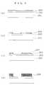
- FIG. 3(A)Film formation was carried out in the present experiment by using a CVD apparatus of the configuration as schematically illustrated in FIG. 3(A).
- 309represents a substantially enclosed reaction vessel capable of substantially maintaining an integral structure composed of a quartz activating chamber 309' and a quartz film forming chamber 309''.
- An exhaust pipe 314, fixed at the end of the film forming chamber 309'',is communicated through an exhaust valve 314' with an exhaust system such as turbo molecular pump (not shown in the figure).
- 307represents a substrate holder, movable back and forth, which is arranged in the film forming chamber 309''.
- 308represents a substrate mounted on the substrate holder 307.
- 307'represents an electric heater to heat the substrate 308, and it is installed inside the substrate holder 307.
- 313represents a microwave applicator which is arranged to underline the circumferential wall surface of the activating chamber 309'.
- a wave guide 313' extending from a source of microwave energyis connected to the microwave applicator 313.
- 304represents a feed pipe made of a stainless-steel for introducing a raw material gas such as SiF4 into the film forming chamber, of which end opens at a position inside the film forming chamber 309'', with no influence of the microwave energy from the microwave applicator 313.
- To the raw material gas feed pipe 304is connected a quartz conduit 301 extending from a raw material gas supply source (not shown in the figure).
- 303represents an electric heater such as resistive heater, which is arranged to envelope the circumferential wall of the quartz conduit 301.
- the film forming raw material gasonce introduced into the quartz conduit 301, is heated to a temperature above 1000°C by the electric heater 303 into an excited state to generate a precursor, which is then transported through the raw material gas feed pipe 304 into the film forming chamber 309'', with no influence of the microwave energy applied by the microwave applicator 313.
- 302represents a hydrogen gas feed pipe extending from a hydrogen gas (H2) source (not shown in the figure) opening at a position upstream the activating chamber 309'.
- H2hydrogen gas
- the hydrogen gas introduced through the hydrogen gas feed pipe 302 into an activating space 305 of the activating chamber 309'is excited by the microwave energy applied through the microwave applicator 313 into the activating space 305, to generate plasma containing active species.
- the plasma thus generatedis then introduced sequentially into the film forming chamber 309'' in order to produce the plasma region shown as the symbol 310.
- the precursor transported through the raw material gas feed pipe 304is discharged from the opening of the raw material gas feed pipe 304 at a position 306 inside the film forming chamber 309'', where the precursor is mixed and contacted with the active species of hydrogen plasma, generated in the activating space 305 of the activating chamber 309' and transported into the film forming chamber, to cause chemical reaction resulting in forming a deposited film on the substrate 308.
- 311is a plasma detector, which is arranged in a freely movable and slidable manner on the circumferential wall of the film forming chamber 309''.
- the detector 311there are disposed slits of 1 mm (width) x 10 mm (length) x 10 mm (depth) in size so as to form two pores at a 10 mm interval, and at the opposite position facing the two pores are arranged probes 311'' composed of optical fibers.
- Each probe 311''is electrically connected through a spectrum analyzer to a feedback circuit, which is electrically connected to a microwave power source.
- the plasma detector 311is located at a position corresponding to the near end of the plasma region described above on the circumferential wall of the film forming chamber 309'', whereby the presence of the emission light having an emission peak at 486 nm is detected, by making the emission light from the hydrogen radicals present in the plasma pass through the pores of the slits 311', detecting the emission light with the probes 311'', and inputting the detected signals into the spectrum analyzer.
- the signals resulting from the detectionis inputted into the feedback circuit, where the necessity of a feedback is judged. In the case where the feedback is required, a feedback signal is reflected over the microwave power source to regulate the microwave energy output from the microwave power source.
- the emission light from hydrogen radicalsdoes not reach the plasma detector 311, so that neither the left nor right spectrum analyzers transmits a signal to the feedback circuit.
- a command signal to increase the microwave output poweris transmitted from the feedback signal to the microwave power source to increase the microwave output power from the microwave power source, and as a result, the plasma region 310 is expanded in the downstream to bring the end thereof to the predetermined position.
- the two spectrum analyzersboth transmit signals to the feedback circuit.
- a command signal to decrease the microwave output poweris transmitted from the feedback circuit to the microwave power source, leading to the reduction in the microwave output power from the microwave power source.
- the state of the plasma region 310, which is produced in the film forming chamber 309''is automatically controlled, in appropriate manner.
- the 312represents a Langumuir probe which is arranged above the opening of the raw material gas feed pipe 304 in the film forming chamber 309'' and of which the electrodes pass heremtically through the circumferential wall of the film forming chamber to be immersed in a plasma.
- the Langmuir probebeing connected to a circuit including a bias source, an ammeter, and a voltmeter, is constituted such that by applying a bias voltage to the electrodes present in the plasma, an electron temperature in the plasma can be measured on the basis of the relationship of an electric current flowing into the electrodes.
- a polycrystalline filmwas formed on the surface of a plane substrate 308 mounted on the substrate holder 307. That is, firstly, a glass plate of a size 20 mm (width) x 60 mm (length) x 1 mm (thickness), manufactured by Corning Glass Works, Article No. 7059, was produced. The glass plate was fixed, laying its longer side in parallel with the gas flow, onto the substrate holder 307, in the way as depicted by numeral reference 308 in FIG. 3(A).
- the inside of the reaction vessel 309was evacuated to a vacuum degree of 1.33 mPa (10 ⁇ 5 Torr).
- the electric heater 307'was actuated to heat the glass plate to 350°C, which was maintained at that temperature.
- SiF4was introduced at a flow rate of 100 sccm into the quartz conduit 301 maintained at 1000°C by the electric furnace 303, and the gas was then transported through the gas feed pipe 304 into the film forming chamber 309''.
- H2 gas and Ar gaswere introduced through the gas feed pipe 302 into the activating chamber 309' at respective flow rates of 200 sccm and 70 sccm, and the two gases were transported into the film forming chamber 309''.
- the pressure inside the reaction vessel 309was brought to about 6.65 Pa (0.05 Torr).
- the microwave power sourcewas switched on to couple the microwave energy of 300 W into the activating chamber 309' through the microwave applicator 313.
- a plasmawas generated in the activating chamber 309', and the plasma region was expanded into the film forming chamber 309''.
- Film formationwas continued for one hour, while holding the end of the plasma region expanding in the film forming chamber 309'' at the position described above, by regulating the microwave power coupled into the activating chamber 309' through the feedback circuit, as has been mentioned above.
- the microwave power sourcewas turned off, the introduction of the three raw material gases were terminated, the electric furnace 303 was turned off, and the glass substrate 308 was cooled to ambient temperature, which was then taken out from the system.
- the glass substratewas cut along its longer side into sections, each in a 10 mm length, to obtain six samples.
- the deposited films on the individual sampleswere observed in terms of film thickness, film crystallinity and crystal grain size in the film.
- the film thicknesswas measured by a feeler-type film thickness instrument (product name; Alpha Step 200, manufactured by Tinker Instrument Co., Ltd.).
- the crystal grain sizewas observed by measuring the size of each of 30 crystal grains within a visual field by using an electron microscope (product name: S-530, manufactured by Hitachi Co., Ltd.) and by examining the mean value of the sizes of 30 crystal grains.
- FIG. 4(A)The results of measurement of film thickness were shown graphically in FIG. 4(A).
- FIG. 4(B)The results of measurement of crystallinity were shown graphically in FIG. 4(B), where relative values were calculated to the peak intensity of X ray diffraction of the deposited film of the 10 mm-long sample obtained by cutting the glass substrate at a position 30 mm from its left end, the peak intensity being designated 1, and the values were plotted in graphs.
- An polycrystalline silicone filmwas formed on the surface of a glass substrate of a size 20 mm (width) x 60 mm (length) x 1 mm (thickness)(manufactured by Corning Glass Works, Article No. 7059), fixed on the substrate holder 307, following the same procedures of Experiment A-1, except that the microwave energy coupled into the activating chamber 309' was not regulated through the foregoing feedback circuit.
- the thickness and crystallinity of the film, and the crystal grain size in the filmwere observed in the same manner as in Experiment A-1.
- FIG. 4(A)The results of measurement of the thickness were shown graphically in FIG. 4(A).
- the results of measurement of the crystallinitywere depicted graphically in FIG. 4(B), where relative values were calculated to the peak intensity of X ray diffraction of the deposited film of the 10 mm-long sample obtained by cutting the glass substrate at a position 30 mm from its left end, the intensity being designated 1, and the values were plotted in graphs.
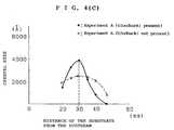
- FIG. 4(C)The observed results with respect to the crystal grain size were shown graphically in FIG. 4(C).
- FIG. 4(A)The results shown in FIG. 4(A) indicate the followings. Regardless of the control of the expansion state of the hydrogen plasma (referred to simply as "plasma” hereinbelow) from the activating chamber into the film forming chamber, the deposition state of the film on the substrate arranged in the film forming chamber is almost the same; the portion closest to the activating chamber, in other words, at the portion of a higher plasma density, the etching action is facilitated more intensely and almost no film deposition occurs; and, at the portions as they become remote from the activating chamber, namely as there occur more reduction in the plasma density, film deposition is enhanced.
- plasmathe portion closest to the activating chamber, in other words, at the portion of a higher plasma density, the etching action is facilitated more intensely and almost no film deposition occurs; and, at the portions as they become remote from the activating chamber, namely as there occur more reduction in the plasma density, film deposition is enhanced.
- the film formed at the end of the plasma regionbecomes such that is not so large in the peak intensity of X ray diffraction, is of a small crystal grain size and not good in crystallinity; but the films formed at the positions as they are apart from said end become such that are large in the peak intensity of X ray diffraction, are large in the crystal grain size, and good in the crystallinity.
- the film formed at the position 10 mm apart from the end of the plasma regionis a polycrystalline film of an extremely good quality which exhibits the largest peak intensity of X ray diffraction and is of the largest crystal grain size (0.4 ⁇ m [4000 Angstroms]).
- the peak intensity of X ray diffractionis small and the crystal grain size is small as well, namely, the crystallinity is not good.
- the film formed at the position more than 40 mm apartbecomes amorphous.
- the end thereof produced in the film forming chamberis varied in a width of about 20 mm, and film formation is initiated at the position of the plasma density getting smaller, i.e. at the position about 20 mm part from the side of the activating chamber in the longitudinal direction with respect to the substrate.
- the films formed at the positions of about 20 mm to about 40 mmbecome such that are not so large in the peak intensity of X ray diffraction and are of about 0.2 ⁇ m (2000-Angstrom) crystal grain size which is not good in the crystallinity.
- the films formed at the positions over 40 mmare such that are small in the peak intensity of X ray diffraction, are even worse in the crystallinity as being mall in crystal grain size, and are amorphous.
- the present inventorattempted to periodically move within a given range the end of a plasma region to be produced in the film forming chamber to form a film in the former case.
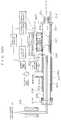
- FIG. 3(C)As the apparatus for film formation, there was used an apparatus shown in FIG. 3(C), comprising the apparatus in the preceding FIG. 3(A), with a plasma detector being added.
- the different point of the apparatus shown in FIG. 3(C) from that shown in FIG. 3(A)is that two plasma detectors 311-1 and 311-2, respectively having the same configuration as that of the plasma detector 311 shown in FIG. 3(A), are arranged side by side in movable and slidable manner on the circumferential wall of the film forming chamber 309'', as shown in FIG. 3(C).
- Each of these detectorsis connected through a circuit composed of two spectrum analyzers and two feedback circuits to an output modulator, which is electrically connected to a microwave power source.
- the plasma detector 311-1was arranged so that the end of a plasma region produced in the film forming chamber 309'' comes to situate at a position of about 1/6 fold distance of a substrate ⁇ 20 mm (width) x 60 mm (length) ⁇ in the longitudinal direction from the side of the activating chamber 309', and the plasma detector 311-2 was arranged so that the end of a plasma region produced in a film forming chamber 309'' comes to situate at a position of about 4/6 fold distance of the substrate in the longitudinal direction as well as in the above case.
- the film forming conditionswere made the same as in Experiment A-1, except the microwave power to be applied into the activating chamber 309'.
- the microwave power to be applied into the activating chamber 309'was made to periodically change between two stages of 250 W and 400 W, at 25 cycles/min. Consequently, the end of a plasma region produced in the film forming chamber 309'' was made to situate at a position of about 1/6 fold distance of the substrate the longitudinal direction as above described in the case of applying microwave power of 250 W, whereas the end of said plasma region was made to situate at a position of about 4/6 fold distance of the substrate in the longitudinal direction in case of applying microwave power of 400 W.
- film formationwas carried out on a glass substrate (No. 7059 glass plate) of 20 mm (width) x 60 mm (length) x 1 mm (thickness) in size, manufactured by Corning Glass Works.
- the period for film formationwas 1 hour.
- the measurement of electron temperature during the film formationindicated 3.2 eV in the case of applying the microwave power of 250 W, and 5.0 eV in the case of applying the microwave power of 400 W.
- the deposited film thus obtainedwas observed in terms of film thickness, peak intensity of X ray diffraction and crystal grain size (mean value), in the same manner as in Experiment A-1.
- the observed results of the film thicknesswere shown graphically in FIG. 5(A).
- FIGs. 5(A), 5(B) and 5(C)indicate the followings. That is, in the case of performing film formation by periodically changing the expansion of the plasma region produced in the film forming chamber on the basis of periodical changes in the microwave power applied in the activating chamber, the state of a film to be deposited on the glass substrate is similar to that in Experiment A. Particularly, at the position closest to the activating chamber, etching is promoted in superior manner and almost no film deposition occurs, but at the positions being remote from the activating chamber, film deposition is enhanced.
- the quality of a film deposited on the glass substratethere is initiated, at a position on the substrate which is slightly over about 10 mm apart from the end of the plasma region produced in film forming chamber, deposition of a polycrystalline film of an identical quality to that of the film exhibiting the largest peak intensity in X ray diffraction and having the largest crystal grain size shown in FIGs. 4(B) and 4(C) which were confirmed in Experiment A-1, and even at a position being about 30 mm apart from said end, there is deposited the foregoing high quality polycrystalline film.
- the microwave power applied into the activating chamberis made to periodically change, whereby periodically changing the expansion of the plasma region to be produced in the film forming chamber, a high quality polycrystalline film may be formed on a large area substrate.
- the film formation in this Experimentwas carried out by using an apparatus of the constitution schematically shown in FIG. 3(B).
- the apparatus shown in FIG. 3(B)has the same configuration as that of the apparatus shown in FIG. 3(A), except that a substrate is held vertically to the gas flow so as to exhaust the gas downward.
- 318represents a substrate holder mounted at the top portion of a transfer shaft 319, capable of moving back and forth through a driving means, if necessary.
- 315represents a substrate arranged on the surface of the substrate holder 318.
- 318'represents a heater for heating the substrate 315 to a predetermined temperature.
- 317represents a stainless-steel flexible wall, integrally constituted through an O-ring along with the circumferential wall of a film forming chamber 309'' made of quartz, in order that the transfer shaft 319 may move back and forth on the circumferential back wall of the film forming chamber 309'', while keeping the sealing condition of the film forming chamber 309''.
- 316represents an exhaust pipe communicated with an exhaust apparatus (not shown in the figure).
- 316'is an exhaust valve, arranged in the exhaust pipe 316.
- the symbol “a”represents the distance between the surface of the substrate 315 and the opening of a raw material gas feed pipe 314 into the film forming chamber 309
- the symbol “b”represents the distance between the surface of the substrate 315 and the end of a plasma region 310.
- a No. 7059 glass plate of 50 mm (width) x 50 mm (length) x 1 mm (thickness) in sizewas used as the substrate 315.
- Table 3The results shown in Table 3 indicate the followings. That is, in the case where the microwave power applied into the activating chamber 309'' is low and the electronic temperature in the plasma is low, film deposition preferentially proceeds with a high film growing speed, but the resulting deposited film becomes such that does not have crystallinity or is inferior in crystallinity. In the case where the microwave power applied into the activating chamber 309' is high and the electronic temperature in the plasma is high, the substrate is exposed to plasma, where no film deposition occors. In the case where the microwave power applied into the activating chamber 309'' is proper, a relatively good balance is provided between the crystallinity and the growing speed of the film to be deposited, but the film obtained is not satisfactory with respect to uniformity. As Table 3 illustrates, a satisfactory film may be obtained under extremely limited film forming conditions.
- Impurities in the deposited film sample No. 305 obtained in Experiment C and the deposited film sample No. 402 obtained in Experiment Dwere analyzed by SIMS. Any impurity was not detected for the former sample, while Cr was detected at 20 ppm for the latter sample. This situation is considered such that Cr is released from the stainless steel member in the inside structure of the reaction vessel 309 due to Cl radicals to contaminate into the film.
- an activation energysuch as microwave energy and a gaseous compound (
- the method for forming a polycrystalline film by the method according to the present inventionis characterized by using hydrogen gas and a film forming raw material gas, contacting the hydrogen gas with an activating energy in a space different from a film forming space of a film forming chamber in which a substrate for film formation is arranged, to excite the hydrogen gas into an active species (H), introducing said active species (H) into the film forming chamber, simultaneously introducing the film forming raw material gas into the film forming chamber, independently from the active species (H), mixing and contacting the active species (H) with the film forming raw material gas to produce a plasma region in the film forming space maintained at a pressure in the range of 0.133 Pa (1 x 10 ⁇ 3 Torr) to 133.322 Pa (1 Torr) and periodically changing the distribution of the concentration of the active species (H) near the surface of the substrate maintained at a temperature of 50°C to 600°C.
- a preferred embodiment of the procedure of repeating the periodical exposure of the substrate to the plasma in the plasma regionis carried out, as was performed in the foregoing Experiment B, by periodically changing the output power of from a power source for an activation energy (microwave energy) to be applied onto the hydrogen gas between a low degree and a high degree, thereby periodically increasing and decreasing the generated amount of the active species (H) having an etching action.
- an activation energymicrowave energy
- the decrease in the amount of the active species (H)correspondingly provides reduction in the expansion of the plasma region in the film forming space to result a state wherein the surface of the substrate does not expose to the plasma, so that film deposition onto the surface of the substrate proceeds superiorly to provide a state where film deposition occurs on said surface (this state will be referred to as "State B" hereinafter).
- the film deposited on the surface of a substrateis etched by a plasma, so that crystallines in a given face orientation are left on the surface of the substrate.
- the State Bfilm deposits on the surface of the substrate where the crystallines in a given face orientation are left, the face orientation of the crystallines grows preferentially.
- the States A and Bare interchangeably repeated to cause the formation of a desirable polycrystalline film containing crystal grains of a large grain size.
- the State Bcontinues for a undesirably long period of time and because of this, the State B transfers to the etching state (i.e. the State A) in the growing progress of crystal grains, thereby reducing the aforementioned etching effect. Consequently, no preferential crystalline growth in a specific orientation does not occur. Therefore, as well as in the former case, it is difficult to obtain a polycrystalline film of a good quality, containing crystalline grains of a large grain size.
- the modulation cycle of the output power sourcein the present invention is preferably 5 to 30 cycles/min, more preferably 10 to 25 cycles/min.
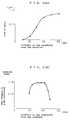
- the aforementioned States A (etching mode) and B (deposition mode) generated by the periodical modulation of the output power source (microwave power source) in the present inventioncan be explained as those provided in the pulse wave form schematically shown in FIG. 6.
- the States A (etching mode) and B (deposition mode)are repeated in the way illustrated with solid lines in FIG. 6. These states are actually repeated as shown with dotted lines.
- the substrate holdermay be moved back and forth through the substrate-holder by a driving apparatus situated outside the vacuum system.
- the cycle of moving back and forth the substratein this case is preferably 5 to 100 cycles/min, more preferably 10 to 40 cycles/min.
- the range of moving back and forth the substrateis preferably 0 to 4 cm, more preferably 0 to 2 cm, from the plasma region.
- the balance between the States A and Bmay be easily maintained even at a rapid cycle, compared with the case of modulating the plasma output.
- the rapid movement within the vacuum systemmay cause to generate dust within the reaction chamber, eventually generating pin holes in a film to be obtained.
- the temperature of the substrate upon forming a desirable polycrystalline film thereon according to the method of the present inventionvaries depending on the kind of a film forming raw material gas to be used, it is 50 to 600°C, preferably 150 to 450°C.
- the inner pressure in the film forming space of the film forming chamber upon film formationis 0.133 Pa (1x10 ⁇ 3 Torr) to 133.332 Pa (1 Torr), preferably 1.33 Pa (1 x 10 ⁇ 2 Torr) to 13.3 Pa (1 x 10 ⁇ 1 Torr).
- the active species having an etching action in the present inventionis principally generated by introducing hydrogen gas into the activating chamber and applying an activation energy (microwave energy) into said chamber to contact the activation energy with the hydrogen gas to thereby excite the hydrogen gas.
- an activation energymicrowave energy
- an inert gassuch as argon gas (Ar gas) and helium gas (He gas)
- the film forming raw material gas to be introduced into the film forming space of the film forming chambermay be introduced into the film forming space as it is.
- the film forming raw material gasis contacted with a suitable activation energy in an activating chamber different from the hydrogen gas activating chamber to thereby decompose the film forming raw material gas to generate a precursor, followed by introducing into the film forming space.
- the activation energymay be any energy such as electric energy including high-frequency energy, thermal energy or light energy.
- polycrystalline semiconductor filmthere can be illustrated, for example, a polycrystalline semiconductor film containing an element of the group IV of the periodic table as a matrix (hereinafter referred to as "group IV polycrystalline semiconductor film"), a polycrystalline semiconductor film containing elements of the groups II and VI of the periodic table as matrixes (hereinafter referred to as "group II-VI polycrystalline semiconductor film”), a polycrystalline semiconductor film containing elements of the groups III and V of the periodic table as matrixes (hereinafter referred to as "group III-V polycrystalline semiconductor film”).
- group IV polycrystalline semiconductor filma polycrystalline semiconductor film containing an element of the group IV of the periodic table as a matrix
- group II-VI polycrystalline semiconductor filma polycrystalline semiconductor film containing elements of the groups II and VI of the periodic table as matrixes
- group III-V polycrystalline semiconductor filma polycrystalline semiconductor film containing elements of the groups III and V of the periodic table as matrixes
- the substrates to be used for forming the foregoing polycrystalline semiconductor film, following the method of the present invention,may be a single crystal substrate or a non-single crystal substrate. They may be conductive or electrically insulating.
- Such substratecan include metals such as Fe, Ni, Cr, Al, Mo, Au, Nb, Ta, V, Ti, Pt, Pb, etc., or alloys thereof, for example, with brass, stainless steel, etc..
- polyesterpolyethylene, polycarbonate, cellulose acetate, polypropylene, polyvinyl chloride, polyvinylidene chloride, polystyrene, polyamide, polyimide, etc., glass and ceramics.
- the single crystal substratethere can be illustrated single crystal substrates of Si, Ge, C, NaCl, KCl, LiF, GaSb, InAs, InSb, GaP, MgO, CaF2, BaF2, ⁇ -Al2O3, etc., being sliced into wafers.
- a compound containing silicon and halogenmay be used.
- Specific example of such compoundare compounds in gaseous state at normal temperature and pressure and easily gasifiable compounds such as SiF4, (SiF2)5, (SiF2)6, (SiF2)4, Si2F6, Si3F8, SiHF3, SiH2F2, SiCl4, (SiCl2)5, SiBr4, (SiBr2)5, Si2Cl6, Si2Br6, SiHCl3, SiH3Cl, SiH2Cl2, SiHBr3, SiHI3, Si2Cl3F3, etc.
- group II-VI polycrystalline semiconductor filmthere are used, as the film forming raw material gases, a compound in gaseous state at normal temperature and pressure or an easily gasifiable compound respectively containing a group II element as the constituent element (hereinafter referred to as "group II compound”), and a compound in gaseous at normal temperature and pressure or an easily gasifiable compound respectively containing a group VI element as the constituent element (hereinafter referred to as "group VI compound”).
- group III-V polycrystalline semiconductor filmthere are used, as the film forming raw material gases, a compound in gaseous state at normal temperature and pressure or an easily gasifiable compound respectively containing a group III element as the constituent element (hereinafter referred to as "group III compound”), and a compound in gaseous state at normal temperature and pressure of an easily gasifiable compound respectively containing a group V element as the constituent element (hereinafter referred to as "group V compound”).
- DMZndimethyl zinc
- DEZndiethyl zinc
- DMCddimethyl cadmium
- DECddiethyl cadmium
- TMAltrimethyl aluminium
- TAAltriethyl aluminium
- TAAltriisobutyl aluminium
- TAAltrimethyl gallium
- TAGatriethyl gallium
- TGatrimethyl indium
- TMIntriethyl indium
- TIntriisobutyl indium
- phosphinePH3
- TBPtertiary-butyl phosphine
- AsH3arsine
- TSAstertiary-butyl arsine
- group VI compoundhydrogen sulfide, methylmercaptane (CH3SH), ethylmercaptane (C2H5SH), propylmercaptane (C3H7SH), selenium hydride (H2Se), dimethyl selenium (DMSe), diethyl selenium (DESe), etc.
- CH3SHmethylmercaptane
- C2H5SHethylmercaptane
- C3H7SHpropylmercaptane
- H2Seselenium hydride
- DMSedimethyl selenium
- DESediethyl selenium
- the gasmay be diluted with hydrogen gas or an inert gas (Ar gas or He gas) before introduction into the precursor-generating space.
- the method of the present invention described abovemay be carried out by using an appropriate so-called HR-CVD (abbreviation of hydrogen assisted chemical vapor deposition) apparatus.
- HR-CVDabbreviation of hydrogen assisted chemical vapor deposition
- a representative example of such apparatusis of the configuration shown schematically in FIG. 1.
- 109represents a substantially enclosed reaction vessel made of quartz which is capable of substantially maintaining an integral structure composed of an activating chamber 109' and a film forming chamber 109'' under vacuum.
- An exhaust pipe 113is arranged at an end of the film forming chamber 109'', and the exhaust pipe is communicated through an exhaust valve 113' with an exhaust system such as turbo molecular pump (not shown in the figure).
- 107represents a substrate holder which is arranged on the tip of a transfer shaft 118 which is capable of moving back and forth and is arranged in the film forming chamber 109''.
- the transfer shaft 108moves back and forth through a sliding system arranged outside the system.
- 114represents a stainless-steel flexible wall integrally constructed with the circumferential wall of the quartz film forming chamber 109'' through an O-ring (not shown in the figure) which can enable the transfer shaft 118 to move back and forth along the circumferential wall of the film forming chamber 109'' while maintaining the film forming chamber 109'' under vacuum.
- 118represents a substrate arranged on the substrate holder 107.
- 107'represents an electric heater arranged inside the substrate holder 107 to heat the substrate 108.
- 117represents a microwave applicator arranged to underline the circumferential wall surface of the activating chamber 109'.
- a wave guide 117'extending from a microwave power source is connected to the microwave applicator 117.
- the 104represents a gas conduit for feeding a raw material gas (A) such as SiF4, into the film forming space of the film forming chamber 109''.
- the gas conduit 104extends toward the film forming space, running horizontally in the center of an activating space 105 of the activating chamber 109', in parallel with the circumferential wall of the activating space, and the end of the conduit opens at the position where the film forming space starts.
- the gas conduit 104is made of a conductive material such as stainless steel.
- the gas conduit 104may be made of an insulating material such as quartz in case where necessary. In this case, the raw material gas (A) during passing through the gas conduit 104 is excited by microwave energy from the microwave applicator 117, which is coupled into the gas conduit.
- a feed pipe 101 for the raw material gas (A) 116extending from a raw material gas reservoir (not shown in the figure).
- 103represents an electric heater such as resistive heater, which is arranged enveloping the circumferential wall of the feed pipe 101.
- the raw material gas (A) supplied through the feed pipe 101is excited by the action of thermal energy from the electric heater to generate a precursor, which is successively supplied through the feed pipe 101 into the film forming chamber 109''.
- the feed pipe 101is made of a heat resistant material such as quartz, ceramics, etc.
- 102represents a supply pipe extending from a reservoir (not shown in the figure) for a raw material gas (B) 115, which opens into the upstream position of the activating chamber 109'.
- the raw material gas (B) introduced through the raw material gas supply pipe 102 into the activating chamber 109'is activated in the activating space 105 by the action of microwave energy applied from the microwave applicator 117, to generate a plasma containing an active species.
- the plasma thus generatedis introduced sequentially into the film forming chamber 109'' to produce a plasma region shown by numeral reference 110.
- the raw material gas (A) or a precursor generated by exciting the raw material gas (A)is transported through the raw material gas feed pipe 104 is released from the opening of the raw material gas feed pipe 104 at a position 106 inside the film forming chamber 109'', where the gas or the precursor is mixed and contacted with the active species from the raw material gas (B), generated in the activating space 105 of the activating chamber 109' and transported thereinto, to cause chemical reaction among them, resulting in forming a deposited film on the substrate 108.
- Plasma detectorsare designated 111-1 and 111-2.
- the two detectors 111-1 and 111-2are disposed side by side in a freely movable and slidable manner on the circumferential wall of the silm forming chamber 109''.
- the two detectors 111-1 and 111-2are of the same configuration. Therefore, explanation will be made on the plasma detector 111-1 below.
- slits 111-1'of 1 mm (width) x 10 mm (length) x 10 mm (depth) in size so as to form two pores at a 10 mm interval, and at the opposite position facing each pore is arranged a probe 111-1'' composed of an optical fiber.
- Each probe 111-1''is electrically connected through a spectrum analyzer to a feedback circuit, which is electrically connected to the microwave power source.
- the plasma detector 111-1is arranged at a position on the circumferential wall of the film forming chamber 109'', the position being situated near the end of the plasma region described above, whereby the presence of the emission light having an emission peak at 486 nm is detected by the spectrum analyzer, by making the light emitted from hydrogen radicals present in the plasma to pass through the pores of the slits 111-1', detecting the emission light with the probes 111-1'', and inputting the detected signals into the spectrum analyzer.
- the signals resulting from the detectionare inputted into the feedback circuit, where the necessity of feedback is judged.
- a feedback signalis reflected over the microwave power source to regulate the microwave output from the microwave power source.
- a signalis outputted only from the spectrum analyzer connected to the left probe while no signal is outputted from the spectrum analyzer connected to the right probe.
- an outputted signalis transmitted to the feedback circuit, but a feedback signal is not transmitted from the feedback circuit to the microwave power source. Therefore in this case, the power of the microwave outputted from the microwave power source is maintained as it is.
- the emission light from hydrogen radicals in the plasmadoes not reach the plasma detector, so that any of the left and right spectrum analyzers does not transmit a signal to the feedback circuit.
- a command signal to increase the microwave output poweris transmitted from the feedback circuit to the microwave power source to increase the microwave energy from the microwave power source.
- the two spectrum analyzerstransmit signals to the feedback circuit.
- a command signal to decrease the microwave output poweris transmitted from the feedback circuit to the microwave power source to cause reduction in the outputted power from the microwave power source.
- the other plasma detector 111-2is of the same configuration as that of the foregoing plasma detector 111-1, and the signal transmission system from the plasma detector 111-2 is the same as that of the plasma detector 111-1.
- the two plasma detectors 111-1 and 111-2are connected, individually through the two spectrum analyzers and two feedback circuits, to an output modulator, which is then electrically connected to the microwave power source.
- the position of the end of the plasma region 110can be moved repeatedly between the optional two positions in the film forming space of the film forming chamber 109'', ", corresponding to the timing of output modulation of the output modulator.
- a desirable position of the plasma region 110is preliminary determined, and the microwave power at the position is measured. High and low microwave powers and the timing information about modulation thereof are inputted into the output modulator. Thereafter, the plasma detectors 111-1 and 111-2 are disposed at desirable positions of the plasma region 110, and the position of the plasma region 110 is regulated through the foregoing feedback system.
- the positional relationship between the substrate 108 and the plasma regionmay be changed by repeating mechanical back and forth movement of the substrate holder 107 through the sliding mechanism outside the system, while fixing the plasma region 110.
- the 112represents a Langumuir probe which is arranged above the opening of the raw material gas feed pipe 104 in the film forming chamber 109'' wherein electrodes pass hermetically through the circumferential wall of the film forming chamber and are immersed in the plasma.
- the Langmuir probebeing connected to a circuit including a bias source, an ammeter, and a voltmeter, is constructed such that by applying a bias voltage to the electrodes present in the plasma, an electron temperature in the plasma can be measured on the basis of the relationship of an electric current flowing into the electrodes.
- Film formationwas performed following the film forming procedures of the foregoing Experiment B, under the film forming conditions shown in Table 5, using the apparatus shown in FIG. 1, to thereby form a polycrystalline silicon deposited film.
- the substrate 108there was used a No. 7059 glass plate of 50 mm (width) x 50 mm (length) x 1 mm (thickness) in size, manufactured by Corning Glass Works.
- the distance between the opening of the conduit 104 and the substrate 108was made to be 6 cm.
- the raw material gas (A) 116SiF4 gas was used.
- the SiF4 gaswas heated to 1100°C by the electric heater 103, introduced at a flow rate of 100 sccm into the feed pipe 101 maintained at this temperature, and supplied through the conduit 104 into the film forming space of the film forming chamber 109''.
- the material gas (B) 115H2 gas and Ar gas were used. The two gases were introduced through the feed pipe 102 into the activating space 105 at respective flow rates of 200 sccm and 70 sccm.
- the application of microwave energy into the activating space 105was carried out by modulating the output power from the microwave power source at two stages of 200 W and 500 W, at 25 cycles/min. At that time, the end of the plasma region to be formed in the film forming space of the film forming chamber 109'' were modulated through the plasma detectors 111-1 and 111-2 , to thereby interchangeably repeat the etching mode and the deposition mode in the pattern shown in FIG. 6.
- the end of the plasma regionwas to reach the surface of the substrate 108 at a 500 W output power of the microwave power source and the plasma region was to end at a position of about 2 cm apart from the substrate 108 at a 200 W output power of the microwave power source, by measuring the emission light of 486 nm from hydrogen radicals.
- the electron temperature of the plasmawas measured by the Langumuir probe 112. The temperature was 60.0 eV in the former case, and it was 2.1 eV in the latter case.
- the film forming processwas continued for 2 hours.
- the film thicknesswas observed in the same manner as in the foregoing Experiment A-1.
- the film thicknesswas 1.1 ⁇ m.
- the size of crystal grain in the filmwas observed in the same manner as in the foregoing Experiment A-1.
- the sizewas 0.5 ⁇ m (5000 Angstroms).
- the Hall mobilitywas observed according to the Van Der Pauw method. As a result, the mobility was found to be 120 - 140 cm2/v.sec almost all over the whole film, indicating that the film is a polycrystalline film of extreme homogeneity.
- Film formationwas performed following the film forming procedures of the foregoing Experiment B under the film forming conditions shown in Table 6, using the apparatus shown in FIG. 1, to thereby form a polycrystalline film of ZnSe.
- the substrate 108there was used a No. 7059 glass plate of 50 mm (width) x 50 mm (length) x 1 mm (thickness) in size, manufactured by Corning Glass Works.
- the distance between the opening of the conduit 104 and the substrate 108was made to be 6.5 cm.
- the film formationwas performed without turning on the electric heater 103.
- a gas generated by flowing hydrogen gas at a flow rate of 40 sccm into diethyl selenium ⁇ (C2H5)2Se ⁇ in a stainless-steel cylinder maintained at 5°C in a thermostatic oven under bubbling condition (not shown in the figure)was introduced through the feed pipe 102 into the activating space. Following the same manner, Ar gas was also introduced in the activating space.
- the application of microwave energy into the activating space 105was carried out by modulating the output power of the microwave power source at two stages of 250 W and 600 W, at 25 cycles/min. At that time, the end of the plasma region formed in the film forming space of the film forming chamber 109'' was modulated through the plasma detectors 111-1 and 111-3, to thereby interchangeably repeat the etching mode and the deposition mode to realize the pattern shown in FIG. 6.
- the end of the plasma regionwas to reach the surface of the substrate 108 at a 500 W output power of the microwave power source, while the plasma region was to end at a position of about 2 cm apart from the substrate 108 at a 200 W output power of the microwave power source, by measuring the emission light of 486 nm from hydrogen radicals.
- the electron temperature of the plasmawas measured by the Langumuir probe 112. The temperature was 5.5 eV in the former case, and it was 1.5 eV in the latter case. The film formation was continued for 2 hours.
- the film thicknesswas observed in the same manner as in the foregoing Experiment A-1. As a result, it was 1.1 ⁇ m.
- the size of crystal grain in the filmwas observed in the same manner as in the foregoing Experiment A-1. As a result, it was 0.6 ⁇ m (6000 Angstroms).
- the Hall mobilitywas observed according to the Van Der Pauw method. As a result, the mobility was found to be 70-90 cm2/v.sec almost all over the whole film, indicating that the film is a polycrystalline film of extreme homogeneity.
- Film formationwas performed under the film forming conditions shown in Table 7, using the apparatus shown in FIG. 1.
- the concentration thereofwas made to change by moving back and forth the substrate to change the relative relationship in position between the substrate and the plasma region, to thereby form a polycrystalline silicon deposited film.
- the substrate 108there was used a No. 7059 glass plate of 50 mm (width) x 50 mm (length) x 1 mm (thickness) in size, manufactured by Corning Glass Works.
- the substrate 108was fixed on the substrate holder 107 movable back and forth through the supporting rod 118 from the outside of the vacuum system.
- the raw material gas (A) 116SiF4 gas was used.
- the SiF4 gasafter heated to 1100°C by the electric heater 103, was introduced at a flow rate of 100 sccm into the feed pipe 101 maintained at this temperature, and the gas was supplied through the conduit 104 into the film forming space of the film forming chamber 109''.
- As the material gas (B) 115H2 gas and Ar gas were used. The two gases were introduced through the feed pipe 102 into the activating space 105 at respective flow rates of 200 sccm and 70 sccm.
- the application of microwave energy into the activating space 105was carried out by fixing the output power of the microwave power source at 300 W.
- the distance between the opening of the conduit 104 and the substratewas set at 6.5 cm at the most apart position, and 4.5 cm at the most closest position.
- the expansion of the plasma regionwas measured. Consequently, it was found that the plasma region expanded from the opening of the conduit 104 to a position of 4.5 cm apart therefrom. Therefore, the substrate was contacted with the plasma region when the substrate was made close to the plasma region; the substrate was positioned 2 cm apart from the plasma region, when it was taken apart from the plasma region.
- the substrateUpon depositing the polycrystalline silicon film, the substrate was made to move back and forth by 2 cm, as described above, at 40 cycles/min, so that the etching mode and the deposition mode were interchangeably repeated.
- the electron temperature of the plasmawas measured by the Langumuir probe 112. The temperature was 4.0 eV. The film formation continued for 2 hours.
- a polycrystalline polysilicon deposited filmwas formed on the glass plate.
- the film thicknesswas observed in the same manner as in the foregoing Experiment A-1. As a result, it was 1.2 ⁇ m.
- the size of crystal grainwas observed in the same manner as in the foregoing Experiment A-1. As a result, it was 0.4 ⁇ m (4000 Angstroms).
- the Hall mobilitywas observed according to the Van Der Pauw method. As a result, the mobility was found to be 100 - 120 cm2/v.sec, almost all over the film, indicating that the film is a polycrystalline film of extreme homogeneity.
- FIG. 7shows the process chart therefor.
- a SiN x film 702was deposited on the substrate with a thickness of 0.2 ⁇ m (2000 Angstroms) by the plasma CVD method ⁇ FIG. 7(a) ⁇ .
- a resistwas subjected to patterning, and the SiN x film was partially removed by a reactive ion etching process, to form a stripped pattern of a 200 ⁇ m width at each 200 ⁇ m interval ⁇ FIG. 7(b) ⁇ .
- the surface comprising the SiN x film 702was a nucleus-forming face, while the surface of the glass substrate 701 was non-nucleus-forming face.
- silicon nucleus 703was selectively generated on the SiN x film 702, according to the CVD method employing plasma ⁇ FIG. 7(c) ⁇ .
- the forming parameterswere as follows: SiF4 100 sccm H2 200 sccm Ar 70 sccm Substrate temperature 350°C Reaction pressure 6.65 Pa (0.05 Torr) Microwave output power (2.45 GHz) modulated interchangeably at 200 and 600 W Output modulation 20 cycles/min
- the end of the plasma regionwas to reach the substrate surface; while with the power being 200 W, the end of the plasma region was to retreat at a position about 2 cm apart from the substrate.
- a polycrystalline polysilicon film 704grew only on the SiN x film, and its thickness was about 1 ⁇ m ⁇ FIG. 7(d) ⁇ .
- Fig. 8shows the process chart therefor.
- a No. 7059 glass plate manufactured by Corning Glass Workswas used as the substrate 801.
- a SiN x film 802was deposited on the substrate with a thickness of 0.2 ⁇ m (2000 Angstroms) by the plasma CVD method ⁇ FIG. 8(a) ⁇ .
- a resist 803was used to form a stripped pattern of a 200 ⁇ m width at each 200 ⁇ m interval. Then, Zn ion 804 was driven, over the pattern by the resist, at 2 x 10¹⁵ ⁇ FIG. 8(b) ⁇ .
- the forming parameterswere as follows; DEZn (carrier H2) 5°C 1 x 10 ⁇ 5 mol/min 30 sccm DESe (carrier H2) 5°C 1 x 10 ⁇ 5 mol/min 40 sccm Ar 30 sccm Substrate temperature 250°C Reaction pressure 6.65 Pa (0.05 Torr) Microwave output power (2.45 GHz) modulated interchangeably at 250 and 700 W Output modulation 20 cycles/min
- a ZnSe polycrystalline film 807grew only on the Zn-ion driving region 805 ⁇ FIG. 8(e) ⁇ , and its film thickness was about 1.2 ⁇ m.
- the ZnSe polycrystalline film grown in the stripe-like statewas subjected to observation by X ray diffraction, indicating that a face (111) was preferentially growing. Furthermore, the grain size was found to be about 0.7 ⁇ m (7000 Angstroms) through observation by a transmission-type electron microscope.
- substrate temperature350°C inner pressure of the film forming chamber 109'' upon film formation 6.65 Pa (0.05 Torr) film formation period 2hours
- Table 6first film-forming raw material gas and its flow rate (C2H5)2Zn gas 1 ⁇ 10 ⁇ 5mol/min H2 gas (carrier gas) 30 sccm second film-forming raw material gas and its flow rate (C2H5)2Se gas 2 ⁇ 10 ⁇ 5mol/min H2 gas (carrier gas) 40 sccm plasma-forming raw material gas and its flow rate H2 gas (serving also as a carrier gas for Se) Ar gas 30 sccm microwave power coupled into the activating chamber 109' (2.45GHz) modulated from 250W to 600W modulation cycle of microwave power 20 cycles/min.
- Table 7 film-forming raw material gas and its flow rate SiF4 gas100 sccm activation temperature of SiF4 gas 1100 °C plasma-forming raw material gas and its flow rate H2 gas 200 sccm Ar gas 70 sccm microwave power coupled into the activating chamber 109' (2.45GHz) 300 W forward and backward moved distance of the substrate 2 cm forward and backward moved cycle of the substrate 40 cycles/min.
- FIG. 1is a schematic explanatory view of a CVD apparatus suitable for practicing the method for forming a polycrystalline deposited film by the chemical vapor deposition process in accordance with the present invention.
- FIGs. 2(a) and 2(g)are schematic explanatory views of the process for selectively forming a polycrystalline deposited film by the method in accordance with the present invention.
- FIGs. 3(A) and 3(C)are schematic explanatory views of CVD apparatuses used in the experiments described in the present specification.
- FIGs. 4(A) and 4(C)are the graphs illustrating the individual results obtained in Experimental A-1 described in the specification.
- FIGs. 5(A) and 5(C)are the graphs illustrating the individual results obtained in Experimental A-2.
- FIG. 6is a schematic explanatory view of the relation between the etching mode and the deposition mode, both being repeated in the method of the present invention.
- FIGs. 7(a) and 7(d)are schematic explanatory views of the process for forming a polycrystalline deposited film in Example 4 of the present invention.
- FIGs. 8(a) and 8(d)are schematic explanatory views of the process for forming a polycrystalline deposited film in Example 5 of the present invention.
Landscapes
- Chemical & Material Sciences (AREA)
- Engineering & Computer Science (AREA)
- General Chemical & Material Sciences (AREA)
- Chemical Kinetics & Catalysis (AREA)
- Materials Engineering (AREA)
- Metallurgy (AREA)
- Organic Chemistry (AREA)
- Mechanical Engineering (AREA)
- Physics & Mathematics (AREA)
- Plasma & Fusion (AREA)
- Crystallography & Structural Chemistry (AREA)
- Chemical Vapour Deposition (AREA)
Abstract
Description
- The present invention relates to an improved method for forming a polycrystalline film useful as a constituent member of electronic devices such as semiconductor device and photovoltaic element, by a chemical vapor deposition process. More specifically, the present invention relates to a method for forming a deposited film, comprising introducing an active species (H) which is obtained by activating hydrogen gas and has an etching action of a deposited film to be formed, a film forming raw material gas having a property to form a deposited film by chemically reacting with the active species (H), or a precursor resulted from the raw material gas, into a film forming chamber where a substrate is installed, and forming therein a deposited film on the surface of the substrate, wherein the active species (H) are introduced into the film forming chamber in such manner that the amount of the active species to be fed onto the surface of the film to be deposited on the substrate is made to change periodically so that the growing speed of the film to be deposited on the substrate periodically changes to chemically react the active species (H) with the film forming raw material or the precursor, in order to form on the substrate a polycrystalline film preferentially grown along a given crystal orientation.
- Polycrystalline deposited films have been drawing recent attention as a constituent member of solar cell, thin-film transistor capable of rapid actuation, as well as large area display, and various types of polycrystalline deposited films have been proposed.
- Such polycrystalline films are formed by film forming techniques such as thermal CVD process, heating vapor deposition method, reactive sputtering technique, molecular beam epitaxial method (referred to as "MBE method" hereinafter), ion plating method, and plasma CVD process. However, any one of these film forming techniques has been indicated to have problems in forming a polycrystalline deposited film. Particularly, according to the thermal CVD method, it is possible to obtain a polycrystalline deposited film to be worth of use, but there is a limit for the kind of a substrate which can be used, since film formation is carried out at elevated temperature.
- In case of the heating vapor deposition method or reactive sputtering method, film formation may be carried out at a relatively low temperature; however, it is difficult to control the crystallinity, crystal orientation and composition ratio of a polycrystalline deposited film to be obtained and thus, it is difficult to stably obtain a desired polycrystalline deposited film.
- In case of the MBE method, a desired polycrystalline deposited film can be obtained at a substantially low temperature, but the inner pressure should necessarily be maintained at an ultra-low pressure (1.33x10⁻⁷ Pa or less [10⁻⁹ Torr or less]) upon film formation, so that the method is not suitable for large-scale production.
- As for the ion plating method, it unavoidably causes ion damages on a film to be deposited, which results in making the resulting polycrystalline deposited film accompanied by a great number of defects, whereby it is difficult to obtain a polycrystalline deposited film of high quality. The method also involves a problem in that it requires a relatively higher temperature at the film formation.
- The plasma CVD method representatively includes microwave plasma CVD method and RF plasma CVD method. According to these plasma CVD methods, a large area polycrystalline deposited film may be possibly formed with the film forming condition of relatively low temperature, but it is extremely difficult to obtain a sufficiently oriented polycrystalline deposited film constantly. Film formation by these plasma CVD methods is carried out in the presence of a plasma, so that a film to be formed is exposed to plasma, whereby causing so-called plasma damage over the film. Because of this, the resulting deposited film often becomes such that is accompanied with many defects.
- For those reasons, there has been proposed a method described in JP-A-62241326 ≡ EP-A-241317, which comprises exciting a film forming raw material with microwave energy in a space different from a film forming space, (namely, an activating space), to generate an active species, transporting the activated species to the film forming space where the activated species is subjected to chemical reaction to thereby deposit a polycrystalline film on a substrate arranged in the film forming space. Particularly, this method comprises exciting in an activating space a film forming raw material gas, namely silicon halide gas, to generate an active species and transporting the active species to the film forming space, simultaneously decomposing other film forming raw material gas in the other activating space to generate other active species, followed by transporting to the film forming space, chemically reacting these active species with each other to form a deposited film on a substrate arranged in the film forming space, wherein a halogen gas or a halogen compound gas, or active species (X) generated by giving an activation energy to them, or active species (principally active species obtained from halogen compound), respectively being capable of exhibiting an etching action to the deposited film, is introduced into the film forming space where crystalline in a given crystal orientation is preferentially grown to form a polycrystalline deposited film.
- Nonetheless, the method involves the following problems. That is: (i) it is extremely difficult to provide uniform distribution of the concentration of the halogen, halogen compound or active species (X) and thus it is difficult to form a homogeneous polycrystalline film having a uniform film thickness on a large area substrate; (ii) it is difficult to maintain the lifetime of the halogen, halogen compound or active species (X), each having an etching action, and the lifetime of the other active species as desired, in order that the both may chemically react together to cause the formation of a film; and (iii) the use of the halogen, halogen compound or active species (x) eventually causes corrosion of the circumferential wall of the film forming space, leading to generation of impurities, which might then be contaminated into a film to be deposited.
- Accordingly, it has been expected eagerly to provide a method which makes it possible to stably form a large area polycrystalline film of high quality which excels in crystal orientation.
- The principal object of the present invention is to solve the foregoing various problems in the known methods for forming a polycrystalline film by chemical vapor deposition process and to provide a method for forming a polycrystalline film satisfying the requirements and expectations described above.
- Another object of the present invention is to provide a chemical vapor deposition method for efficiently forming a polycrystalline film, the film being useful as a constituent member of electronic elements such as semiconductor device and photovoltaic element, due to excellent electric properties, homogeneity and uniform thickness, and superior adhesion not only to a substrate but also to other deposited films.
- Still another object of the present invention is to provide a chemical vapor deposition method for efficiently forming a polycrystalline film over a large area, the film containing crystal grains of a large grain size without containing impurities, being homogeneous and uniform in thickness and having a higher degree of the Hall mobility.
- Through the experiments described hereinbelow, the present inventor has made studies in order to solve the foregoing problems in the known CVD methods for forming a polycrystalline film and in order to attain the above objects. Consequently, the inventors have obtained findings such that a desirable polycrystalline film, preferentially grown in a given orientation and of a high quality with a large crystal size, may be formed on a substrate, principally by contacting hydrogen gas with an activation energy to excite the gas, introducing the resulting active species (H) having an etching action for a deposited film to be formed, along with a film forming raw material gas having the property to chemically react with the active species (H) to form a deposited film, or with a precursor obtained from the raw material gas, into a film forming chamber wherein the substrate is arranged, and chemically reacting the active species (H) with the film forming raw material gas or the precursor, wherein the introduction of the active species into the film forming chamber is carried out such that the amount of the active species (H) fed onto the surface of a film being growing on the substrate is periodically made to change in order to change the growing speed of the film to be deposited on the substrate.
- The present invention has been achieved based on the above findings which the present inventor has obtained through the experiments. The gist of the present invention is of the contents as described hereinbelow. That is, a method for forming a polycrystalline film, characterized by using hydrogen gas and a film forming raw material gas, contacting the hydrogen gas with an activating energy in a space different from a film forming space of a film forming chamber in which a substrate for film formation is arranged, to excite the hydrogen gas into an active species (H), introducing said active species (H) into the film forming chamber, simultaneously introducing the film forming raw material gas into the film forming chamber, independently from the active species (H), mixing and contacting the active species (H) with the film forming raw material gas to produce a plasma region in the film forming space maintained at a pressure in the range of 0.133 Pa (1 x 10⁻³ Torr) to 133.322 Pa (1 Torr) and periodically changing the distribution of the concentration of the active species (H) near the surface of the substrate maintained at a temperature of 50°C to 600°C.
- According to the present invention thus constituted, crystalline in a given orientation is preferentially grown to efficiently form a desirable polycrystalline film on a substrate, said film containing crystal grains of a large size in a desirable state, without containing impurities, being homogeneous and uniform in thickness, having an excellent adhesion not only to the substrate but also to other deposited film, exhibiting a large Hall mobility, and thus being useful as a constituent element of electronic devices such as semiconductor devices, photovoltaic elements, etc.
- The experiments performed by the inventor will now be explained hereinafter.
- The present inventor has selected the method for forming a polycrystalline film, comprising introducing gaseous active species (H) consisting of hydrogen radical and a film forming raw material gas or a precursor obtained by exciting the raw material gas with an activation energy, having the property to chemically react with the active species (H) to form a deposited film, into a film forming space where a substrate is arranged, and subsequently reacting the gaseous active species (H) with the film forming raw material gas or the precursor. And the following experiments were performed, in order to investigate whether or not there causes some influences over the properties of a polycrystalline film to be formed on the substrate depending upon the relationship between the zone (referred to as "plasma zone" hereinafter) where there exists the gaseous active species (H) having an etching action and being formed in the film forming chamber and the position where the substrate is arranged.
- Film formation was carried out in the present experiment by using a CVD apparatus of the configuration as schematically illustrated in FIG. 3(A). In FIG. 3(A), 309 represents a substantially enclosed reaction vessel capable of substantially maintaining an integral structure composed of a quartz activating chamber 309' and a quartz film forming chamber 309''. An
exhaust pipe 314, fixed at the end of the film forming chamber 309'', is communicated through an exhaust valve 314' with an exhaust system such as turbo molecular pump (not shown in the figure). 307 represents a substrate holder, movable back and forth, which is arranged in the film forming chamber 309''. 308 represents a substrate mounted on thesubstrate holder 307. 307' represents an electric heater to heat thesubstrate 308, and it is installed inside thesubstrate holder 307. 313 represents a microwave applicator which is arranged to underline the circumferential wall surface of the activating chamber 309'. A wave guide 313' extending from a source of microwave energy is connected to themicrowave applicator 313. 304 represents a feed pipe made of a stainless-steel for introducing a raw material gas such as SiF₄ into the film forming chamber, of which end opens at a position inside the film forming chamber 309'', with no influence of the microwave energy from themicrowave applicator 313. To the raw materialgas feed pipe 304 is connected aquartz conduit 301 extending from a raw material gas supply source (not shown in the figure). 303 represents an electric heater such as resistive heater, which is arranged to envelope the circumferential wall of thequartz conduit 301. The film forming raw material gas, once introduced into thequartz conduit 301, is heated to a temperature above 1000°C by theelectric heater 303 into an excited state to generate a precursor, which is then transported through the raw materialgas feed pipe 304 into the film forming chamber 309'', with no influence of the microwave energy applied by themicrowave applicator 313. 302 represents a hydrogen gas feed pipe extending from a hydrogen gas (H₂) source (not shown in the figure) opening at a position upstream the activating chamber 309'. The hydrogen gas introduced through the hydrogengas feed pipe 302 into an activatingspace 305 of the activating chamber 309' is excited by the microwave energy applied through themicrowave applicator 313 into the activatingspace 305, to generate plasma containing active species. The plasma thus generated is then introduced sequentially into the film forming chamber 309'' in order to produce the plasma region shown as thesymbol 310. - The precursor transported through the raw material
gas feed pipe 304 is discharged from the opening of the raw materialgas feed pipe 304 at aposition 306 inside the film forming chamber 309'', where the precursor is mixed and contacted with the active species of hydrogen plasma, generated in the activatingspace 305 of the activating chamber 309' and transported into the film forming chamber, to cause chemical reaction resulting in forming a deposited film on thesubstrate 308. - 311 is a plasma detector, which is arranged in a freely movable and slidable manner on the circumferential wall of the film forming chamber 309''. In the
detector 311, there are disposed slits of 1 mm (width) x 10 mm (length) x 10 mm (depth) in size so as to form two pores at a 10 mm interval, and at the opposite position facing the two pores are arranged probes 311'' composed of optical fibers. Each probe 311'' is electrically connected through a spectrum analyzer to a feedback circuit, which is electrically connected to a microwave power source. Theplasma detector 311 is located at a position corresponding to the near end of the plasma region described above on the circumferential wall of the film forming chamber 309'', whereby the presence of the emission light having an emission peak at 486 nm is detected, by making the emission light from the hydrogen radicals present in the plasma pass through the pores of the slits 311', detecting the emission light with the probes 311'', and inputting the detected signals into the spectrum analyzer. The signals resulting from the detection is inputted into the feedback circuit, where the necessity of a feedback is judged. In the case where the feedback is required, a feedback signal is reflected over the microwave power source to regulate the microwave energy output from the microwave power source. More specifically, when the end of theplasma region 301 produced in the film forming chamber 309'' resides at a predetermined position, namely, between the two probes of the plasma detector, a signal is outputted only from the spectrum analyzer connected to the left probe while no signal is outputted from the spectrum analyzer connected to the right probe. In this case, a signal outputted is transmitted to the feedback circuit, but a feedback signal is not transmitted from the feedback circuit to the microwave power source. Therefore in this case, the microwave energy from the microwave power source is maintained as it is. - When the end of the
plasma region 301 resides upstream the predetermined position due to the small area of theplasma region 301, the emission light from hydrogen radicals does not reach theplasma detector 311, so that neither the left nor right spectrum analyzers transmits a signal to the feedback circuit. In this case, a command signal to increase the microwave output power is transmitted from the feedback signal to the microwave power source to increase the microwave output power from the microwave power source, and as a result, theplasma region 310 is expanded in the downstream to bring the end thereof to the predetermined position. When theplasma region 310 expands downstream, that is, the end of the microwave region expands over the predetermined position, the two spectrum analyzers both transmit signals to the feedback circuit. In this case, a command signal to decrease the microwave output power is transmitted from the feedback circuit to the microwave power source, leading to the reduction in the microwave output power from the microwave power source. In such manner, the state of theplasma region 310, which is produced in the film forming chamber 309'', is automatically controlled, in appropriate manner. - 312 represents a Langumuir probe which is arranged above the opening of the raw material
gas feed pipe 304 in the film forming chamber 309'' and of which the electrodes pass heremtically through the circumferential wall of the film forming chamber to be immersed in a plasma. The Langmuir probe, being connected to a circuit including a bias source, an ammeter, and a voltmeter, is constituted such that by applying a bias voltage to the electrodes present in the plasma, an electron temperature in the plasma can be measured on the basis of the relationship of an electric current flowing into the electrodes. - Under the film forming conditions shown in Table 1, using the foregoing apparatus shown in FIG. 3(A), a polycrystalline film was formed on the surface of a
plane substrate 308 mounted on thesubstrate holder 307. That is, firstly, a glass plate of asize 20 mm (width) x 60 mm (length) x 1 mm (thickness), manufactured by Corning Glass Works, Article No. 7059, was produced. The glass plate was fixed, laying its longer side in parallel with the gas flow, onto thesubstrate holder 307, in the way as depicted bynumeral reference 308 in FIG. 3(A). Then, by actuating the exhaust system (not shown in the figure) after opening the exhaust valve 314', the inside of thereaction vessel 309 was evacuated to a vacuum degree of 1.33 mPa (10⁻⁵ Torr). The electric heater 307' was actuated to heat the glass plate to 350°C, which was maintained at that temperature. Subsequently, SiF₄ was introduced at a flow rate of 100 sccm into thequartz conduit 301 maintained at 1000°C by theelectric furnace 303, and the gas was then transported through thegas feed pipe 304 into the film forming chamber 309''. Concurrently, H₂ gas and Ar gas were introduced through thegas feed pipe 302 into the activating chamber 309' at respective flow rates of 200 sccm and 70 sccm, and the two gases were transported into the film forming chamber 309''. By regulating the opening of the exhaust valve 314', the pressure inside thereaction vessel 309 was brought to about 6.65 Pa (0.05 Torr). When the individual flow rates of the three gases (SiF₄ gas, H₂ gas and Ar gas) became stable at the values defined above, the microwave power source was switched on to couple the microwave energy of 300 W into the activating chamber 309' through themicrowave applicator 313. A plasma was generated in the activating chamber 309', and the plasma region was expanded into the film forming chamber 309''. As a result of observing the end of the plasma in the film forming chamber 309'' by the spectrum analyzers shown in FIG. 3(A), it was situated at a position (namely, at the end of the glass plate on the side of the activating chamber 309') 20 mm apart from the left end of the glass plate (substrate 308) mounted on thesubstrate holder 307. An electron temperature in the plasma was measured by theLangumuir probe 312 shown in FIG. 3(A). It was 3.9 eV. - Film formation was continued for one hour, while holding the end of the plasma region expanding in the film forming chamber 309'' at the position described above, by regulating the microwave power coupled into the activating chamber 309' through the feedback circuit, as has been mentioned above.
- The foregoing film forming conditions were collectively shown in Table 1.
- After completion of the film formation, the microwave power source was turned off, the introduction of the three raw material gases were terminated, the
electric furnace 303 was turned off, and theglass substrate 308 was cooled to ambient temperature, which was then taken out from the system. The glass substrate was cut along its longer side into sections, each in a 10 mm length, to obtain six samples. The deposited films on the individual samples were observed in terms of film thickness, film crystallinity and crystal grain size in the film. The film thickness was measured by a feeler-type film thickness instrument (product name; Alpha Step 200, manufactured by Tinker Instrument Co., Ltd.). Crystallinity was observed by measuring a peak intensity of X ray diffraction at 2ϑ = 47.3° (CuKα is used as the source) with a X ray diffractometer (product name; RAD IIB, manufactured by Rigaku Denki K.K.). The crystal grain size was observed by measuring the size of each of 30 crystal grains within a visual field by using an electron microscope (product name: S-530, manufactured by Hitachi Co., Ltd.) and by examining the mean value of the sizes of 30 crystal grains. - The results of measurement of film thickness were shown graphically in FIG. 4(A). The results of measurement of crystallinity were shown graphically in FIG. 4(B), where relative values were calculated to the peak intensity of X ray diffraction of the deposited film of the 10 mm-long sample obtained by cutting the glass substrate at a
position 30 mm from its left end, the peak intensity being designated 1, and the values were plotted in graphs. - The results of the observation with respect to crystal grains were shown graphically in FIG. 4(C).
- An polycrystalline silicone film was formed on the surface of a glass substrate of a
size 20 mm (width) x 60 mm (length) x 1 mm (thickness)(manufactured by Corning Glass Works, Article No. 7059), fixed on thesubstrate holder 307, following the same procedures of Experiment A-1, except that the microwave energy coupled into the activating chamber 309' was not regulated through the foregoing feedback circuit. - Regarding the polycrystalline silicone film formed on the glass substrate, the thickness and crystallinity of the film, and the crystal grain size in the film were observed in the same manner as in Experiment A-1.
- The results of measurement of the thickness were shown graphically in FIG. 4(A). The results of measurement of the crystallinity were depicted graphically in FIG. 4(B), where relative values were calculated to the peak intensity of X ray diffraction of the deposited film of the 10 mm-long sample obtained by cutting the glass substrate at a
position 30 mm from its left end, the intensity being designated 1, and the values were plotted in graphs. The observed results with respect to the crystal grain size were shown graphically in FIG. 4(C). - The results shown in FIG. 4(A) indicate the followings. Regardless of the control of the expansion state of the hydrogen plasma (referred to simply as "plasma" hereinbelow) from the activating chamber into the film forming chamber, the deposition state of the film on the substrate arranged in the film forming chamber is almost the same; the portion closest to the activating chamber, in other words, at the portion of a higher plasma density, the etching action is facilitated more intensely and almost no film deposition occurs; and, at the portions as they become remote from the activating chamber, namely as there occur more reduction in the plasma density, film deposition is enhanced.
- However, as the results shown in FIGs. 4(B) and 4(C) illustrate, a significant difference is caused between the quality of a film to be formed in the case where it is formed while holding the end of the plasma region produced in the film forming chamber at the predetermined position (Experiment A-1) and the quality of a film to be formed in the case where it is formed without controlling said end (Experiment A-2). In other words, in the former case, the film formed at the end of the plasma region becomes such that is not so large in the peak intensity of X ray diffraction, is of a small crystal grain size and not good in crystallinity; but the films formed at the positions as they are apart from said end become such that are large in the peak intensity of X ray diffraction, are large in the crystal grain size, and good in the crystallinity. The film formed at the position 10 mm apart from the end of the plasma region is a polycrystalline film of an extremely good quality which exhibits the largest peak intensity of X ray diffraction and is of the largest crystal grain size (0.4 µm [4000 Angstroms]). Regarding the film formed at the position over 10 mm apart and about 40 mm apart from the end of the plasma region, the peak intensity of X ray diffraction is small and the crystal grain size is small as well, namely, the crystallinity is not good. The film formed at the position more than 40 mm apart becomes amorphous.
- On the other hand, in the latter case wherein the film is formed without regulating the end of the plasma region (namely, Experiment A-2), the end thereof produced in the film forming chamber is varied in a width of about 20 mm, and film formation is initiated at the position of the plasma density getting smaller, i.e. at the position about 20 mm part from the side of the activating chamber in the longitudinal direction with respect to the substrate. And the films formed at the positions of about 20 mm to about 40 mm become such that are not so large in the peak intensity of X ray diffraction and are of about 0.2 µm (2000-Angstrom) crystal grain size which is not good in the crystallinity. The films formed at the positions over 40 mm are such that are small in the peak intensity of X ray diffraction, are even worse in the crystallinity as being mall in crystal grain size, and are amorphous.
- Consequently, for any of the films formed in the latter case, there is not such a case as in the former case that becomes the largest with respect to the peak intensity of X ray diffraction and the crystal grain size, and there is a significant difference with respect to the film quality in comparison with the polycrystalline films formed in the former case which are the largest with respect to the peak intensity of X ray diffraction and the crystal grain size. However, in the latter case, it is possible to form a polycrystalline film of a practically applicable film quality in the wide range in the longitudinal direction of the substrate.
- The following findings were confirmed in Experiment A:
- (i) when film formation is carried out by controlling the expansion state of the plasma region from the activating chamber into the film forming chamber to hold the end thereof at the predetermined position by way of regulating the microwave power applied into the activating chamber, the film deposited at a specific position of the substrate becomes a polycrystalline film excelling in the quality, exhibiting an extremely large peak intensity in X ray diffraction and having a very large crystal grain size; and
- (ii) when film formation is carried out without controlling the end of the plasma region extending from the activating chamber into the film forming chamber, a practically applicable polycrystalline film can be obtained over the wide range of the substrate, in the longitudinal direction.
- Based on those facts (i) and (ii), the present inventor attempted to periodically move within a given range the end of a plasma region to be produced in the film forming chamber to form a film in the former case.
- As the apparatus for film formation, there was used an apparatus shown in FIG. 3(C), comprising the apparatus in the preceding FIG. 3(A), with a plasma detector being added. In other words, the different point of the apparatus shown in FIG. 3(C) from that shown in FIG. 3(A) is that two plasma detectors 311-1 and 311-2, respectively having the same configuration as that of the
plasma detector 311 shown in FIG. 3(A), are arranged side by side in movable and slidable manner on the circumferential wall of the film forming chamber 309'', as shown in FIG. 3(C). Each of these detectors is connected through a circuit composed of two spectrum analyzers and two feedback circuits to an output modulator, which is electrically connected to a microwave power source. - The plasma detector 311-1 was arranged so that the end of a plasma region produced in the film forming chamber 309'' comes to situate at a position of about 1/6 fold distance of a substrate {20 mm (width) x 60 mm (length)} in the longitudinal direction from the side of the activating chamber 309', and the plasma detector 311-2 was arranged so that the end of a plasma region produced in a film forming chamber 309'' comes to situate at a position of about 4/6 fold distance of the substrate in the longitudinal direction as well as in the above case.
- The film forming conditions were made the same as in Experiment A-1, except the microwave power to be applied into the activating chamber 309'. The microwave power to be applied into the activating chamber 309' was made to periodically change between two stages of 250 W and 400 W, at 25 cycles/min. Consequently, the end of a plasma region produced in the film forming chamber 309'' was made to situate at a position of about 1/6 fold distance of the substrate the longitudinal direction as above described in the case of applying microwave power of 250 W, whereas the end of said plasma region was made to situate at a position of about 4/6 fold distance of the substrate in the longitudinal direction in case of applying microwave power of 400 W.
- In this way, film formation was carried out on a glass substrate (No. 7059 glass plate) of 20 mm (width) x 60 mm (length) x 1 mm (thickness) in size, manufactured by Corning Glass Works. The period for film formation was 1 hour. The measurement of electron temperature during the film formation indicated 3.2 eV in the case of applying the microwave power of 250 W, and 5.0 eV in the case of applying the microwave power of 400 W. The deposited film thus obtained was observed in terms of film thickness, peak intensity of X ray diffraction and crystal grain size (mean value), in the same manner as in Experiment A-1. The observed results of the film thickness were shown graphically in FIG. 5(A). The observed results of the peak intensity in X ray diffraction were shown graphically in FIG. 5(B), where relative values were calculated to the highest value shown in FIG. 4(B) defined as 1. The observed results of the crystal grain size were shown in FIG. 5(C).
- The results shown in FIGs. 5(A), 5(B) and 5(C) indicate the followings. That is, in the case of performing film formation by periodically changing the expansion of the plasma region produced in the film forming chamber on the basis of periodical changes in the microwave power applied in the activating chamber, the state of a film to be deposited on the glass substrate is similar to that in Experiment A. Particularly, at the position closest to the activating chamber, etching is promoted in superior manner and almost no film deposition occurs, but at the positions being remote from the activating chamber, film deposition is enhanced. As for the quality of a film deposited on the glass substrate, there is initiated, at a position on the substrate which is slightly over about 10 mm apart from the end of the plasma region produced in film forming chamber, deposition of a polycrystalline film of an identical quality to that of the film exhibiting the largest peak intensity in X ray diffraction and having the largest crystal grain size shown in FIGs. 4(B) and 4(C) which were confirmed in Experiment A-1, and even at a position being about 30 mm apart from said end, there is deposited the foregoing high quality polycrystalline film. According, as described above, in the case where the microwave power applied into the activating chamber is made to periodically change, whereby periodically changing the expansion of the plasma region to be produced in the film forming chamber, a high quality polycrystalline film may be formed on a large area substrate.
- In this Experiment, based on the results obtained in Experiments A and B, the state of film deposition on a substrate was observed while changing the relative positional relationship between the end of a plasma region produced in the film forming chamber and the substrate.
- The film formation in this Experiment was carried out by using an apparatus of the constitution schematically shown in FIG. 3(B). The apparatus shown in FIG. 3(B) has the same configuration as that of the apparatus shown in FIG. 3(A), except that a substrate is held vertically to the gas flow so as to exhaust the gas downward. 318 represents a substrate holder mounted at the top portion of a
transfer shaft 319, capable of moving back and forth through a driving means, if necessary. 315 represents a substrate arranged on the surface of thesubstrate holder 318. 318' represents a heater for heating thesubstrate 315 to a predetermined temperature. 317 represents a stainless-steel flexible wall, integrally constituted through an O-ring along with the circumferential wall of a film forming chamber 309'' made of quartz, in order that thetransfer shaft 319 may move back and forth on the circumferential back wall of the film forming chamber 309'', while keeping the sealing condition of the film forming chamber 309''. 316 represents an exhaust pipe communicated with an exhaust apparatus (not shown in the figure). 316' is an exhaust valve, arranged in theexhaust pipe 316. - In FIG. 3(B), the symbol "a" represents the distance between the surface of the
substrate 315 and the opening of a raw materialgas feed pipe 314 into thefilm forming chamber 309, and the symbol "b" represents the distance between the surface of thesubstrate 315 and the end of aplasma region 310. - In the present Experiment, a No. 7059 glass plate of 50 mm (width) x 50 mm (length) x 1 mm (thickness) in size, manufactured by Corning Glass Works, was used as the
substrate 315. - Following the procedures of Experiment A, film formation was carried out under the film forming conditions shown in Table 2, except that the distance between the "a" and the "b" was changed as shown in Table 3, and that the microwave power applied into the activating chamber 309' was changed as shown in Table 3, to thereby obtain 16 samples of deposited films (Sample Nos. 301 to 316).
- The electron temperature in the plasma during the formation of each of the 16 deposited film samples was measured in the same manner as in Experimental A-1. The results were shown in Table 3.
- For each of the resultant deposited film samples, there were observed film thickness, crystallinity, uniformity and Hall mobility. The film thickness and crystallinity of the film were observed in the same manner as in Experiment A-1, and the results obtained were shown in Table 3. The crystallinity of the film was shown in Table 3, as "present" when a peak appeared in X ray diffraction at a crystalline angle 2ϑ = 47.3° or "absent" when the peak did not appear. The observation of the film uniformity was carried out as follows; film thickness was firstly measured at 4 points 5 mm inside from each side of the substrate and at the center thereof, following the same procedures as in Experiment A-1. In Table 3, the case where the coefficients of variation of the film thickness measured at the 5 points are less than is represented as "○" and the case where the coefficients of variation are more than said figure are represented as "X". The Hall mobility was measured according to the Van Der Pauw method, and the results observed were shown in Table 3.
- The results shown in Table 3 indicate the followings. That is, in the case where the microwave power applied into the activating chamber 309'' is low and the electronic temperature in the plasma is low, film deposition preferentially proceeds with a high film growing speed, but the resulting deposited film becomes such that does not have crystallinity or is inferior in crystallinity. In the case where the microwave power applied into the activating chamber 309' is high and the electronic temperature in the plasma is high, the substrate is exposed to plasma, where no film deposition occors. In the case where the microwave power applied into the activating chamber 309'' is proper, a relatively good balance is provided between the crystallinity and the growing speed of the film to be deposited, but the film obtained is not satisfactory with respect to uniformity. As Table 3 illustrates, a satisfactory film may be obtained under extremely limited film forming conditions.
- In this Experiment, film formation was performed, employing the individual film forming conditions for the three deposited film samples Nos. 13, 15 and 19, and using the apparatus shown in FIG. 3(B) and Cl₂ known as a gas having an etching action, in addition to H₂ gas and Ar gas. As for the Cl₂ gas, there was provided Cl₂ gas diluted with H₂ gas to 500 ppm, namely Cl₂/H₂ gas (=500 ppm). The flow of the Cl₂/H₂ gas was adjusted as shown in Table 4, and it was introduced together with H₂ gas and Ar gas through the
feed pipe 302 into the activating chamber 309'. The film forming conditions other than those described above, were made as shown in Table 2. In this way, there were prepared 6 deposited film samples (samples Nos. 401 to 406) as shown in Table 4. - For each of the deposited film samples thus obtained, film thickness, crystallinity and uniformity of the film, and Hall mobility were observed in the same manner as in Experiment C. The results of the observation are shown in Table 4 as in Experiment C.
- The results shown in Table 4 indicate the followings. That is; in the case where the electron temperature in plasma is 2.5 or 4.1 eV (i.e. in the case of the sample No. 303 or 305) in Experiment C, there is observed neither crystallinity nor Hall mobility for the deposited films. However, there is observed both crystallinity and Hall mobility for the films deposited with the introduction of Cl₂ gas, wherein the films are, however, contaminated with impurities and their Hall mobilities are not satisfactory. In the case where the electron temperature in plasma is 5.2 eV (i.e. in the case of the sample No. 309) in Experiment C, there is observed both crystallinity and satisfactory Hall mobility for the deposited film. However, said Hall mobility of the deposited film is remarkably reduced to be unsatisfactory when Cl₂ gas is introduced upon its formation. As for the thickness of the film to be deposited, it is decreased in any case, compared with the cases of Experiment C.
- Impurities in the deposited film sample No. 305 obtained in Experiment C and the deposited film sample No. 402 obtained in Experiment D were analyzed by SIMS. Any impurity was not detected for the former sample, while Cr was detected at 20 ppm for the latter sample. This situation is considered such that Cr is released from the stainless steel member in the inside structure of the
reaction vessel 309 due to Cl radicals to contaminate into the film. - From the foregoing results obtained in Experiments A to D, the followings were recognized.
- In the case of simultaneously introducing an active species (H) having an etching action which is generated by exciting hydrogen gas with an activation energy such as microwave energy and a gaseous compound (namely, a film forming raw material gas) containing an element to be a constituent of a film to be formed which reacts with the active species (H) or a precursor generated by exciting the film forming raw material gas with an activation energy such as thermal energy into a film forming space wherein a substrate on which a film to be deposited is placed producing a plasma region in the film forming space, and periodically repeating the procedures of exposing and unveiling the substrate to the plasma in the plasma region, there is established interchangeably the state where film deposition superiorly proceeds and the state where the etching of the film proceeds superiorly than the film deposition, resulting in preferential growth of the face orientation of crystalline which is advantageous for growth of the film, whereby forming a desirable polycrystalline film containing crystal grains of a large grain size, without containing impurities.
- The method for forming a polycrystalline film by the method according to the present invention is characterized by using hydrogen gas and a film forming raw material gas, contacting the hydrogen gas with an activating energy in a space different from a film forming space of a film forming chamber in which a substrate for film formation is arranged, to excite the hydrogen gas into an active species (H), introducing said active species (H) into the film forming chamber, simultaneously introducing the film forming raw material gas into the film forming chamber, independently from the active species (H), mixing and contacting the active species (H) with the film forming raw material gas to produce a plasma region in the film forming space maintained at a pressure in the range of 0.133 Pa (1 x 10⁻³ Torr) to 133.322 Pa (1 Torr) and periodically changing the distribution of the concentration of the active species (H) near the surface of the substrate maintained at a temperature of 50°C to 600°C.
- A preferred embodiment of the procedure of repeating the periodical exposure of the substrate to the plasma in the plasma region is carried out, as was performed in the foregoing Experiment B, by periodically changing the output power of from a power source for an activation energy (microwave energy) to be applied onto the hydrogen gas between a low degree and a high degree, thereby periodically increasing and decreasing the generated amount of the active species (H) having an etching action. In this procedure of the present invention, the increase in the amount of the active species (H) having an etching action, which is generated from hydrogen gas, correspondingly provides expansion of the plasma region to be produced in the film forming space to cause the substrate to expose to the plasma, so that on the surface of the substrate is generated the state where etching is effected superiorly than film deposition thereon (this state will be referred to as "State A" hereinafter). On the other hand, the decrease in the amount of the active species (H) correspondingly provides reduction in the expansion of the plasma region in the film forming space to result a state wherein the surface of the substrate does not expose to the plasma, so that film deposition onto the surface of the substrate proceeds superiorly to provide a state where film deposition occurs on said surface (this state will be referred to as "State B" hereinafter). In the State A, the film deposited on the surface of a substrate is etched by a plasma, so that crystallines in a given face orientation are left on the surface of the substrate. In the State B, film deposits on the surface of the substrate where the crystallines in a given face orientation are left, the face orientation of the crystallines grows preferentially. In the present invention, the States A and B are interchangeably repeated to cause the formation of a desirable polycrystalline film containing crystal grains of a large grain size.
- When the cycle of repeating the States A and B, namely, the modulation cycle of an output power source for the activation energy which is applied in the activating space in order to generate the active species (H) from hydrogen gas, is too short, the change of the plasma region cannot follow the output power change and as a result, there is not provided a desirable plasma region to cause a breakpoint between the States A and B. In this case, the preferential crystalline growth in a specific orientation and the increase in the crystal grain size are not brought about. Thus, there cannot be obtained a polycrystalline film of good quality, containing crystal grains of a large crystal grain size, which is intended to provide by the present invention. When the modulation cycle of the output power source is too long, the state of film deposition (i.e. the State B) continues for a undesirably long period of time and because of this, the State B transfers to the etching state (i.e. the State A) in the growing progress of crystal grains, thereby reducing the aforementioned etching effect. Consequently, no preferential crystalline growth in a specific orientation does not occur. Therefore, as well as in the former case, it is difficult to obtain a polycrystalline film of a good quality, containing crystalline grains of a large grain size.
- Therefore, the modulation cycle of the output power source, in the present invention is preferably 5 to 30 cycles/min, more preferably 10 to 25 cycles/min.
- The aforementioned States A (etching mode) and B (deposition mode) generated by the periodical modulation of the output power source (microwave power source) in the present invention can be explained as those provided in the pulse wave form schematically shown in FIG. 6. In a preferred embodiment, the States A (etching mode) and B (deposition mode) are repeated in the way illustrated with solid lines in FIG. 6. These states are actually repeated as shown with dotted lines.
- In order to interchangeably provide the State A (etching mode) and the State B (deposition mode) on the surface of the substrate, it is possible to employ another method comprising making the substrate holder move back and forth while fixing the plasma region to thereby change the relative positional relationship between the plasma region and the substrate. In this case, the substrate holder may be moved back and forth through the substrate-holder by a driving apparatus situated outside the vacuum system. The cycle of moving back and forth the substrate in this case is preferably 5 to 100 cycles/min, more preferably 10 to 40 cycles/min. The range of moving back and forth the substrate is preferably 0 to 4 cm, more preferably 0 to 2 cm, from the plasma region.
- According to this method, the balance between the States A and B may be easily maintained even at a rapid cycle, compared with the case of modulating the plasma output. However, it should be noted that the rapid movement within the vacuum system may cause to generate dust within the reaction chamber, eventually generating pin holes in a film to be obtained.
- The temperature of the substrate upon forming a desirable polycrystalline film thereon according to the method of the present invention varies depending on the kind of a film forming raw material gas to be used, it is 50 to 600°C, preferably 150 to 450°C.
- The inner pressure in the film forming space of the film forming chamber upon film formation is 0.133 Pa (1x10⁻³ Torr) to 133.332 Pa (1 Torr), preferably 1.33 Pa (1 x 10⁻² Torr) to 13.3 Pa (1 x 10⁻¹ Torr).
- The active species having an etching action in the present invention is principally generated by introducing hydrogen gas into the activating chamber and applying an activation energy (microwave energy) into said chamber to contact the activation energy with the hydrogen gas to thereby excite the hydrogen gas. At that time, in addition to the hydrogen gas, it is possible to introduce an inert gas such as argon gas (Ar gas) and helium gas (He gas) into the activating chamber, wherein it is excited together with the hydrogen gas with the action of the activation energy to thereby generate active species (H) having an etching action, and introduce the active species (H) into the activating space of the activating chamber. In this case, discharge to decompose the hydrogen gas in the activating chamber is stabilized and the a plasma region produced in the film forming space of the film forming chamber is stabilized.
- In the method of the present invention, the film forming raw material gas to be introduced into the film forming space of the film forming chamber may be introduced into the film forming space as it is. In a preferred embodiment, the film forming raw material gas is contacted with a suitable activation energy in an activating chamber different from the hydrogen gas activating chamber to thereby decompose the film forming raw material gas to generate a precursor, followed by introducing into the film forming space.
- The activation energy may be any energy such as electric energy including high-frequency energy, thermal energy or light energy.
- According to the method of the present invention, various kinds of polycrystalline semiconductor films may be formed efficiently. As such polycrystalline semiconductor film, there can be illustrated, for example, a polycrystalline semiconductor film containing an element of the group IV of the periodic table as a matrix (hereinafter referred to as "group IV polycrystalline semiconductor film"), a polycrystalline semiconductor film containing elements of the groups II and VI of the periodic table as matrixes (hereinafter referred to as "group II-VI polycrystalline semiconductor film"), a polycrystalline semiconductor film containing elements of the groups III and V of the periodic table as matrixes (hereinafter referred to as "group III-V polycrystalline semiconductor film").
- The substrates to be used for forming the foregoing polycrystalline semiconductor film, following the method of the present invention, may be a single crystal substrate or a non-single crystal substrate. They may be conductive or electrically insulating.
- Specific examples of such substrate can include metals such as Fe, Ni, Cr, Al, Mo, Au, Nb, Ta, V, Ti, Pt, Pb, etc., or alloys thereof, for example, with brass, stainless steel, etc..
- In addition to those described above, there can include synthetic resins in a film or sheet form, including polyester, polyethylene, polycarbonate, cellulose acetate, polypropylene, polyvinyl chloride, polyvinylidene chloride, polystyrene, polyamide, polyimide, etc., glass and ceramics.
- As the single crystal substrate, there can be illustrated single crystal substrates of Si, Ge, C, NaCl, KCl, LiF, GaSb, InAs, InSb, GaP, MgO, CaF₂, BaF₂, α-Al₂O₃, etc., being sliced into wafers.
- For example, in the case of forming a group IV polycrystalline semiconductor film, a compound containing silicon and halogen may be used. Specific example of such compound are compounds in gaseous state at normal temperature and pressure and easily gasifiable compounds such as SiF₄, (SiF₂)₅, (SiF₂)₆, (SiF₂)₄, Si₂F₆, Si₃F₈, SiHF₃, SiH₂F₂, SiCl₄, (SiCl₂)₅, SiBr₄, (SiBr₂)₅, Si₂Cl₆, Si₂Br₆, SiHCl₃, SiH₃Cl, SiH₂Cl₂, SiHBr₃, SiHI₃, Si₂Cl₃F₃, etc.
- In the case of forming a group II-VI polycrystalline semiconductor film, there are used, as the film forming raw material gases, a compound in gaseous state at normal temperature and pressure or an easily gasifiable compound respectively containing a group II element as the constituent element (hereinafter referred to as "group II compound"), and a compound in gaseous at normal temperature and pressure or an easily gasifiable compound respectively containing a group VI element as the constituent element (hereinafter referred to as "group VI compound").
- In the case of forming a group III-V polycrystalline semiconductor film, there are used, as the film forming raw material gases, a compound in gaseous state at normal temperature and pressure or an easily gasifiable compound respectively containing a group III element as the constituent element (hereinafter referred to as "group III compound"), and a compound in gaseous state at normal temperature and pressure of an easily gasifiable compound respectively containing a group V element as the constituent element (hereinafter referred to as "group V compound").
- Specific example of the aforementioned group II compound are dimethyl zinc (DMZn), diethyl zinc (DEZn), dimethyl cadmium (DMCd), diethyl cadmium (DECd), etc.
- Specific example of the aforementioned group III compound are trimethyl aluminium (TMAl), triethyl aluminium (TEAl), triisobutyl aluminium (TBAl), trimethyl gallium (TMGa), triethyl gallium (TEGa), trimethyl indium (TMIn), triethyl indium (TEIn), triisobutyl indium (TBIn), etc.
- Specific example of the aforementioned group V compound are phosphine (PH₃), tertiary-butyl phosphine (TBP), arsine (AsH₃), tertiary-butyl arsine (TBAs), etc.
- Specific example of the aforementioned group VI compound are hydrogen sulfide, methylmercaptane (CH₃SH), ethylmercaptane (C₂H₅SH), propylmercaptane (C₃H₇SH), selenium hydride (H₂Se), dimethyl selenium (DMSe), diethyl selenium (DESe), etc.
- In the case where the foregoing film forming raw material gas is decomposed with an activation energy into a precursor before introduction into the film forming chamber, the gas may be diluted with hydrogen gas or an inert gas (Ar gas or He gas) before introduction into the precursor-generating space.
- The method of the present invention described above may be carried out by using an appropriate so-called HR-CVD (abbreviation of hydrogen assisted chemical vapor deposition) apparatus. A representative example of such apparatus is of the configuration shown schematically in FIG. 1.
- The apparatus shown in FIG. 1 will now be explained. 109 represents a substantially enclosed reaction vessel made of quartz which is capable of substantially maintaining an integral structure composed of an activating chamber 109' and a film forming chamber 109'' under vacuum. An
exhaust pipe 113 is arranged at an end of the film forming chamber 109'', and the exhaust pipe is communicated through an exhaust valve 113' with an exhaust system such as turbo molecular pump (not shown in the figure). 107 represents a substrate holder which is arranged on the tip of atransfer shaft 118 which is capable of moving back and forth and is arranged in the film forming chamber 109''. Thetransfer shaft 108 moves back and forth through a sliding system arranged outside the system. 114 represents a stainless-steel flexible wall integrally constructed with the circumferential wall of the quartz film forming chamber 109'' through an O-ring (not shown in the figure) which can enable thetransfer shaft 118 to move back and forth along the circumferential wall of the film forming chamber 109'' while maintaining the film forming chamber 109'' under vacuum. 118 represents a substrate arranged on thesubstrate holder 107. 107' represents an electric heater arranged inside thesubstrate holder 107 to heat thesubstrate 108. 117 represents a microwave applicator arranged to underline the circumferential wall surface of the activating chamber 109'. A wave guide 117' extending from a microwave power source is connected to themicrowave applicator 117. 104 represents a gas conduit for feeding a raw material gas (A) such as SiF₄, into the film forming space of the film forming chamber 109''. Thegas conduit 104 extends toward the film forming space, running horizontally in the center of an activatingspace 105 of the activating chamber 109', in parallel with the circumferential wall of the activating space, and the end of the conduit opens at the position where the film forming space starts. Thegas conduit 104 is made of a conductive material such as stainless steel. Thegas conduit 104 may be made of an insulating material such as quartz in case where necessary. In this case, the raw material gas (A) during passing through thegas conduit 104 is excited by microwave energy from themicrowave applicator 117, which is coupled into the gas conduit. To thegas conduit 104 is connected afeed pipe 101 for the raw material gas (A) 116, extending from a raw material gas reservoir (not shown in the figure). 103 represents an electric heater such as resistive heater, which is arranged enveloping the circumferential wall of thefeed pipe 101. The raw material gas (A) supplied through thefeed pipe 101 is excited by the action of thermal energy from the electric heater to generate a precursor, which is successively supplied through thefeed pipe 101 into the film forming chamber 109''. In this case, thefeed pipe 101 is made of a heat resistant material such as quartz, ceramics, etc. 102 represents a supply pipe extending from a reservoir (not shown in the figure) for a raw material gas (B) 115, which opens into the upstream position of the activating chamber 109'. The raw material gas (B) introduced through the raw materialgas supply pipe 102 into the activating chamber 109' is activated in the activatingspace 105 by the action of microwave energy applied from themicrowave applicator 117, to generate a plasma containing an active species. The plasma thus generated is introduced sequentially into the film forming chamber 109'' to produce a plasma region shown bynumeral reference 110. - The raw material gas (A) or a precursor generated by exciting the raw material gas (A) is transported through the raw material
gas feed pipe 104 is released from the opening of the raw materialgas feed pipe 104 at aposition 106 inside the film forming chamber 109'', where the gas or the precursor is mixed and contacted with the active species from the raw material gas (B), generated in the activatingspace 105 of the activating chamber 109' and transported thereinto, to cause chemical reaction among them, resulting in forming a deposited film on thesubstrate 108. - Plasma detectors are designated 111-1 and 111-2. The two detectors 111-1 and 111-2 are disposed side by side in a freely movable and slidable manner on the circumferential wall of the silm forming chamber 109''. The two detectors 111-1 and 111-2 are of the same configuration. Therefore, explanation will be made on the plasma detector 111-1 below. In the detector 111, there are arranged slits 111-1' of 1 mm (width) x 10 mm (length) x 10 mm (depth) in size so as to form two pores at a 10 mm interval, and at the opposite position facing each pore is arranged a probe 111-1'' composed of an optical fiber. Each probe 111-1'' is electrically connected through a spectrum analyzer to a feedback circuit, which is electrically connected to the microwave power source. The plasma detector 111-1 is arranged at a position on the circumferential wall of the film forming chamber 109'', the position being situated near the end of the plasma region described above, whereby the presence of the emission light having an emission peak at 486 nm is detected by the spectrum analyzer, by making the light emitted from hydrogen radicals present in the plasma to pass through the pores of the slits 111-1', detecting the emission light with the probes 111-1'', and inputting the detected signals into the spectrum analyzer. The signals resulting from the detection are inputted into the feedback circuit, where the necessity of feedback is judged. In case where the feedback is required, a feedback signal is reflected over the microwave power source to regulate the microwave output from the microwave power source. Referring specifically, when the end of the
plasma region 110 produced in the film forming chamber 109'' resides at the predetermined position, namely, between the two probes of the plasma detector, a signal is outputted only from the spectrum analyzer connected to the left probe while no signal is outputted from the spectrum analyzer connected to the right probe. In this case, an outputted signal is transmitted to the feedback circuit, but a feedback signal is not transmitted from the feedback circuit to the microwave power source. Therefore in this case, the power of the microwave outputted from the microwave power source is maintained as it is. - When the end of the
plasma region 110 resides upstream the predetermined position due to the smallness of theplasma region 110, the emission light from hydrogen radicals in the plasma does not reach the plasma detector, so that any of the left and right spectrum analyzers does not transmit a signal to the feedback circuit. In this case, a command signal to increase the microwave output power is transmitted from the feedback circuit to the microwave power source to increase the microwave energy from the microwave power source. When theplasma region 110 expands downstream, that is, the end of the microwave energy region exapnds beyond the predetermined position, the two spectrum analyzers transmit signals to the feedback circuit. In this case, a command signal to decrease the microwave output power is transmitted from the feedback circuit to the microwave power source to cause reduction in the outputted power from the microwave power source. - The other plasma detector 111-2 is of the same configuration as that of the foregoing plasma detector 111-1, and the signal transmission system from the plasma detector 111-2 is the same as that of the plasma detector 111-1. The two plasma detectors 111-1 and 111-2 are connected, individually through the two spectrum analyzers and two feedback circuits, to an output modulator, which is then electrically connected to the microwave power source.
- Since the apparatus is constructed as described above, the position of the end of the
plasma region 110 can be moved repeatedly between the optional two positions in the film forming space of the film forming chamber 109'', ", corresponding to the timing of output modulation of the output modulator. - Particularly, a desirable position of the
plasma region 110 is preliminary determined, and the microwave power at the position is measured. High and low microwave powers and the timing information about modulation thereof are inputted into the output modulator. Thereafter, the plasma detectors 111-1 and 111-2 are disposed at desirable positions of theplasma region 110, and the position of theplasma region 110 is regulated through the foregoing feedback system. - The positional relationship between the
substrate 108 and the plasma region may be changed by repeating mechanical back and forth movement of thesubstrate holder 107 through the sliding mechanism outside the system, while fixing theplasma region 110. - 112 represents a Langumuir probe which is arranged above the opening of the raw material
gas feed pipe 104 in the film forming chamber 109'' wherein electrodes pass hermetically through the circumferential wall of the film forming chamber and are immersed in the plasma. The Langmuir probe, being connected to a circuit including a bias source, an ammeter, and a voltmeter, is constructed such that by applying a bias voltage to the electrodes present in the plasma, an electron temperature in the plasma can be measured on the basis of the relationship of an electric current flowing into the electrodes. - The present invention will be explained more detailed with reference the following examples, but the invention is not limited to these Examples.
- Film formation was performed following the film forming procedures of the foregoing Experiment B, under the film forming conditions shown in Table 5, using the apparatus shown in FIG. 1, to thereby form a polycrystalline silicon deposited film.
- As the
substrate 108, there was used a No. 7059 glass plate of 50 mm (width) x 50 mm (length) x 1 mm (thickness) in size, manufactured by Corning Glass Works. - The distance between the opening of the
conduit 104 and thesubstrate 108 was made to be 6 cm. As the raw material gas (A) 116, SiF₄ gas was used. The SiF₄ gas was heated to 1100°C by theelectric heater 103, introduced at a flow rate of 100 sccm into thefeed pipe 101 maintained at this temperature, and supplied through theconduit 104 into the film forming space of the film forming chamber 109''. As the material gas (B) 115, H₂ gas and Ar gas were used. The two gases were introduced through thefeed pipe 102 into the activatingspace 105 at respective flow rates of 200 sccm and 70 sccm. The application of microwave energy into the activatingspace 105 was carried out by modulating the output power from the microwave power source at two stages of 200 W and 500 W, at 25 cycles/min. At that time, the end of the plasma region to be formed in the film forming space of the film forming chamber 109'' were modulated through the plasma detectors 111-1 and 111-2 , to thereby interchangeably repeat the etching mode and the deposition mode in the pattern shown in FIG. 6. Particularly, regarding the plasma region formed in the film forming space of the film forming chamber 109'', the end of the plasma region was to reach the surface of thesubstrate 108 at a 500 W output power of the microwave power source and the plasma region was to end at a position of about 2 cm apart from thesubstrate 108 at a 200 W output power of the microwave power source, by measuring the emission light of 486 nm from hydrogen radicals. In the two cases, the electron temperature of the plasma was measured by theLangumuir probe 112. The temperature was 60.0 eV in the former case, and it was 2.1 eV in the latter case. The film forming process was continued for 2 hours. - On the glass plate was formed a polycrystalline silicon deposited film. Of the deposited film, the film thickness, the size of crystal grain and the Hall mobility were observed. The film thickness was observed in the same manner as in the foregoing Experiment A-1. The film thickness was 1.1 µm. The size of crystal grain in the film was observed in the same manner as in the foregoing Experiment A-1. As a result, the size was 0.5 µm (5000 Angstroms). The Hall mobility was observed according to the Van Der Pauw method. As a result, the mobility was found to be 120 - 140 cm²/v.sec almost all over the whole film, indicating that the film is a polycrystalline film of extreme homogeneity.
- Film formation was performed following the film forming procedures of the foregoing Experiment B under the film forming conditions shown in Table 6, using the apparatus shown in FIG. 1, to thereby form a polycrystalline film of ZnSe.
- As the
substrate 108, there was used a No. 7059 glass plate of 50 mm (width) x 50 mm (length) x 1 mm (thickness) in size, manufactured by Corning Glass Works. The distance between the opening of theconduit 104 and thesubstrate 108 was made to be 6.5 cm. - In this example, the film formation was performed without turning on the
electric heater 103. Into theconduit 101, there was introduced a gas produced by flowing hydrogen gas at a flow rate of 30 sccm into diethyl zinc [(C₂H₅)₂Zn] contained in a stainless steel cylinder maintained at 5°C in a thermostatic oven under bubbling condition, which was successively supplied through theconduit 104 into the film forming space of the film forming chamber 109''. A gas generated by flowing hydrogen gas at a flow rate of 40 sccm into diethyl selenium {(C₂H₅)₂Se} in a stainless-steel cylinder maintained at 5°C in a thermostatic oven under bubbling condition (not shown in the figure) was introduced through thefeed pipe 102 into the activating space. Following the same manner, Ar gas was also introduced in the activating space. - The application of microwave energy into the activating
space 105 was carried out by modulating the output power of the microwave power source at two stages of 250 W and 600 W, at 25 cycles/min. At that time, the end of the plasma region formed in the film forming space of the film forming chamber 109'' was modulated through the plasma detectors 111-1 and 111-3, to thereby interchangeably repeat the etching mode and the deposition mode to realize the pattern shown in FIG. 6. Particularly, regarding the plasma region formed in the film forming space of the film forming chamber 109'', the end of the plasma region was to reach the surface of thesubstrate 108 at a 500 W output power of the microwave power source, while the plasma region was to end at a position of about 2 cm apart from thesubstrate 108 at a 200 W output power of the microwave power source, by measuring the emission light of 486 nm from hydrogen radicals. In the two cases, the electron temperature of the plasma was measured by theLangumuir probe 112. The temperature was 5.5 eV in the former case, and it was 1.5 eV in the latter case. The film formation was continued for 2 hours. - On the glass place was formed a polycrystalline ZnSe deposited film. Of the deposited film, the film thickness, the size of crystal grain and the Hall mobility were observed. The film thickness was observed in the same manner as in the foregoing Experiment A-1. As a result, it was 1.1 µm. The size of crystal grain in the film was observed in the same manner as in the foregoing Experiment A-1. As a result, it was 0.6 µm (6000 Angstroms). The Hall mobility was observed according to the Van Der Pauw method. As a result, the mobility was found to be 70-90 cm²/v.sec almost all over the whole film, indicating that the film is a polycrystalline film of extreme homogeneity.
- Film formation was performed under the film forming conditions shown in Table 7, using the apparatus shown in FIG. 1.
- In this example, instead of modulating the output power of the microwave power source so as to change the concentration of the active species on the substrate, the concentration thereof was made to change by moving back and forth the substrate to change the relative relationship in position between the substrate and the plasma region, to thereby form a polycrystalline silicon deposited film.
- As the
substrate 108, there was used a No. 7059 glass plate of 50 mm (width) x 50 mm (length) x 1 mm (thickness) in size, manufactured by Corning Glass Works. - The
substrate 108 was fixed on thesubstrate holder 107 movable back and forth through the supportingrod 118 from the outside of the vacuum system. As the raw material gas (A) 116, SiF₄ gas was used. The SiF₄ gas after heated to 1100°C by theelectric heater 103, was introduced at a flow rate of 100 sccm into thefeed pipe 101 maintained at this temperature, and the gas was supplied through theconduit 104 into the film forming space of the film forming chamber 109''. As the material gas (B) 115, H₂ gas and Ar gas were used. The two gases were introduced through thefeed pipe 102 into the activatingspace 105 at respective flow rates of 200 sccm and 70 sccm. The application of microwave energy into the activatingspace 105 was carried out by fixing the output power of the microwave power source at 300 W. The distance between the opening of theconduit 104 and the substrate was set at 6.5 cm at the most apart position, and 4.5 cm at the most closest position. By observing the emission light of 486 nm from hydrogen radicals through the plasma detector 111-1, the expansion of the plasma region was measured. Consequently, it was found that the plasma region expanded from the opening of theconduit 104 to a position of 4.5 cm apart therefrom. Therefore, the substrate was contacted with the plasma region when the substrate was made close to the plasma region; the substrate was positioned 2 cm apart from the plasma region, when it was taken apart from the plasma region. - Upon depositing the polycrystalline silicon film, the substrate was made to move back and forth by 2 cm, as described above, at 40 cycles/min, so that the etching mode and the deposition mode were interchangeably repeated. The electron temperature of the plasma was measured by the
Langumuir probe 112. The temperature was 4.0 eV. The film formation continued for 2 hours. - In the manner described above, a polycrystalline polysilicon deposited film was formed on the glass plate. Of the deposited film obtained, the film thickness, the size of crystal grain and the hall mobility were observed. The film thickness was observed in the same manner as in the foregoing Experiment A-1. As a result, it was 1.2 µm. The size of crystal grain was observed in the same manner as in the foregoing Experiment A-1. As a result, it was 0.4 µm (4000 Angstroms). The Hall mobility was observed according to the Van Der Pauw method. As a result, the mobility was found to be 100 - 120 cm²/v.sec, almost all over the film, indicating that the film is a polycrystalline film of extreme homogeneity.
- In this example, selective deposition of a polysilicon film was performed according to the method of the present invention.
- FIG. 7 shows the process chart therefor.
- Using a No. 7059 glass plate manufactured by Corning Glass Works, as the
substrate 701, a SiNx film 702 was deposited on the substrate with a thickness of 0.2 µm (2000 Angstroms) by the plasma CVD method {FIG. 7(a)}. The deposition conditions were as follows; substrate temperature: 350°C, reaction pressure: 26.67 Pa (0.2 Torr), RF power: 5W, raw material gas: SiH₄ gas = 100 sccm, NH₃ gas = 200 sccm. - By using a conventional photolithography technique, a resist was subjected to patterning, and the SiNx film was partially removed by a reactive ion etching process, to form a stripped pattern of a 200 µm width at each 200 µm interval {FIG. 7(b)}. Herein, the surface comprising the SiNx film 702 was a nucleus-forming face, while the surface of the
glass substrate 701 was non-nucleus-forming face. - On the substrate thus processed
silicon nucleus 703 was selectively generated on the SiNx film 702, according to the CVD method employing plasma {FIG. 7(c)}. - The CVD method employed was the same as in Example 1 {FIG. 7(c)}.
- The forming parameters were as follows:
SiF₄ 100 sccm H₂ 200 sccm Ar 70 sccm Substrate temperature 350°C Reaction pressure 6.65 Pa (0.05 Torr) Microwave output power (2.45 GHz) modulated interchangeably at 200 and 600 W Output modulation 20 cycles/min - When the output power of the microwave power source was 600 W, the end of the plasma region was to reach the substrate surface; while with the power being 200 W, the end of the plasma region was to retreat at a position about 2 cm apart from the substrate.
- After 2-hour deposition in such manner, a
polycrystalline polysilicon film 704 grew only on the SiNx film, and its thickness was about 1 µm {FIG. 7(d)}. The depositedfilm 704 grown in stripes was subjected to observation by X ray diffraction. Only an intense peak with a crystalline angle 2ϑ = 47.3° was observed, indicating that a face (220) was preferentially growing. Furthermore, the grain size was found to be about 0.5 µm (5000 Angstroms) through observation by a transmission-type electron microscope. - In this example, selective deposition of a polycrystalline ZnSe film was performed according to the method of the present invention.
- Fig. 8 shows the process chart therefor.
- A No. 7059 glass plate manufactured by Corning Glass Works was used as the
substrate 801. A SiNx film 802 was deposited on the substrate with a thickness of 0.2 µm (2000 Angstroms) by the plasma CVD method {FIG. 8(a)}. The depositing conditions were as follows; substrate temperature: 350°C, reaction pressure: 26.67 Pa (0.2 Torr), RF power: 5W, raw material gas: SiH₄ gas = 100 sccm, NH₃ gas = 200 sccm. - By using the photolithography technique, a resist 803 was used to form a stripped pattern of a 200 µm width at each 200 µm interval. Then,
Zn ion 804 was driven, over the pattern by the resist, at 2 x 10¹⁵ {FIG. 8(b)}. - After scaling off the resist, there was formed a SiNx film 805 where Zn ion was driven into the exposed portion {FIG. 8(a)}.
- On the substrate thus processed, selective deposition of a polycrystalline ZnSe film was carried out according to the same method as in Example 2.
- The forming parameters were as follows;
DEZn (carrier H₂) 5°C 1 x 10⁻⁵ mol/ min 30 sccm DESe (carrier H₂) 5°C 1 x 10⁻⁵ mol/ min 40 sccm Ar 30 sccm Substrate temperature 250°C Reaction pressure 6.65 Pa (0.05 Torr) Microwave output power (2.45 GHz) modulated interchangeably at 250 and 700 W Output modulation 20 cycles/min - When the output power of the microwave power source was 700 W, the end of the plasma region reached the substrate surface; while with the power being 250 W, the end of the plasma region retreated at a position about 2 cm apart from the substrate. By such manner, a
nucleus 806 of ZnSe polycrystalline was generated only in the Zn-ion driving region 805 on the substrate {FIG. 8(d)}. - After 2-hour deposition in such manner, a ZnSe
polycrystalline film 807 grew only on the Zn-ion driving region 805 {FIG. 8(e)}, and its film thickness was about 1.2 µm. The ZnSe polycrystalline film grown in the stripe-like state was subjected to observation by X ray diffraction, indicating that a face (111) was preferentially growing. Furthermore, the grain size was found to be about 0.7 µm (7000 Angstroms) through observation by a transmission-type electron microscope.Table 1 film-forming raw material gas and its flow rate SiF₄ gas 100 sccm activation temperature of SiF₄ gas 1100 °C plasma-forming raw material gas and its flow rate H₂ gas 200 sccm Ar gas 70 sccm microwave power coupled into the activating chamber 309' (2.45GHz) 300 W substrate temperature 350°C inner pressure of the film forming chamber 309'' upon film formation 6.65 Pa (0.05 Torr) film formation period 1hour Table 2 film-forming raw material gas and its flow rate SiF₄ gas 100 sccm activation temperature of SiF₄ gas 1100 °C plasma-forming raw material gas and its flow rate H₂ gas 100 sccm Ar gas 50 sccm microwave power coupled into the activating chamber 309' (2.45GHz) see Table 3 substrate temperature 350°C inner pressure of the film forming chamber 309'' upon film formation 2.667 Pa (0.02 Torr) film formation period 1hour 

Table 5 film-forming raw material gas and its flow rate SiF₄ gas 100 sccm activation temperature of SiF₄ gas 1100 °C plasma-forming raw material gas and its flow rate H₂ gas 200 sccm Ar gas 70 sccm microwave power coupled into the activating chamber 109' (2.45GHz) modulated from 200W to 500W modulation cycle of microwave power 25 cycles/min. substrate temperature 350°C inner pressure of the film forming chamber 109'' upon film formation 6.65 Pa (0.05 Torr) film formation period 2hours Table 6 first film-forming raw material gas and its flow rate (C₂H₅)₂Zn gas 1 × 10⁻⁵mol/min H₂ gas (carrier gas) 30 sccm second film-forming raw material gas and its flow rate (C₂H₅) ₂Se gas 2 × 10⁻⁵mol/min H₂ gas (carrier gas) 40 sccm plasma-forming raw material gas and its flow rate H₂ gas (serving also as a carrier gas for Se) Ar gas 30 sccm microwave power coupled into the activating chamber 109' (2.45GHz) modulated from 250W to 600W modulation cycle of microwave power 20 cycles/min. substrate temperature 250°C inner pressure of the film forming chamber 109'' upon film formation 13.3 Pa (0.1 Torr) film formation period 2hours Table 7 film-forming raw material gas and its flow rate SiF₄ gas 100 sccm activation temperature of SiF₄ gas 1100 °C plasma-forming raw material gas and its flow rate H₂ gas 200 sccm Ar gas 70 sccm microwave power coupled into the activating chamber 109' (2.45GHz) 300 W forward and backward moved distance of the substrate 2 cm forward and backward moved cycle of the substrate 40 cycles/min. substrate temperature 350°C inner pressure of the film forming chamber 109'' upon film formation 6.65 Pa (0.05 Torr) film formation period 2hours - FIG. 1 is a schematic explanatory view of a CVD apparatus suitable for practicing the method for forming a polycrystalline deposited film by the chemical vapor deposition process in accordance with the present invention.
- FIGs. 2(a) and 2(g) are schematic explanatory views of the process for selectively forming a polycrystalline deposited film by the method in accordance with the present invention.
- FIGs. 3(A) and 3(C) are schematic explanatory views of CVD apparatuses used in the experiments described in the present specification.
- FIGs. 4(A) and 4(C) are the graphs illustrating the individual results obtained in Experimental A-1 described in the specification.
- FIGs. 5(A) and 5(C) are the graphs illustrating the individual results obtained in Experimental A-2.
- FIG. 6 is a schematic explanatory view of the relation between the etching mode and the deposition mode, both being repeated in the method of the present invention.
- FIGs. 7(a) and 7(d) are schematic explanatory views of the process for forming a polycrystalline deposited film in Example 4 of the present invention.
- FIGs. 8(a) and 8(d) are schematic explanatory views of the process for forming a polycrystalline deposited film in Example 5 of the present invention.


Claims (6)
- A method for forming a polycrystalline film, characterized by using hydrogen gas and a film forming raw material gas, contacting the hydrogen gas with an activating energy in a space different from a film forming space of a film forming chamber in which a substrate for film formation is arranged, to excite the hydrogen gas into an active species (H), introducing said active species (H) into the film forming chamber, simultaneously introducing the film forming raw material gas into the film forming chamber, independently from the active species (H), mixing and contacting the active species (H) with the film forming raw material gas to produce a plasma region in the film forming space maintained at a pressure in the range of 0.133 Pa (1 x 10⁻³ Torr) to 133.322 Pa (1 Torr) and periodically changing the distribution of the concentration of the active species (H) near the surface of the substrate maintained at a temperature of 50°C to 600°C.
- The method according to Claim 1, wherein the expansion of the plasma region formed in the film forming space is periodically increased and decreased by periodic modulation of the output power of the activating energy from a power source to periodically expose the substrate intermittently to the plasma region.
- The method according to Claim 2, wherein the activating energy is microwave energy.
- The method according to Claim 1, wherein an inert gas is contacted with the activating energy together with the hydrogen gas to excite them in order to generate the active species (H).
- The method according to Claim 1, wherein the film forming raw material gas is excited with an activating energy to generate a precursor and the precursor is introduced into the film forming space.
- The method according to Claim 1, wherein the film forming process comprising periodically changing the distribution of the concentration of the active species (H) is carried out while moving the substrate back and forth.
Applications Claiming Priority (5)
| Application Number | Priority Date | Filing Date | Title |
|---|---|---|---|
| JP8110789 | 1989-03-31 | ||
| JP81107/89 | 1989-03-31 | ||
| JP247262/89 | 1989-09-22 | ||
| JP24726289 | 1989-09-22 | ||
| PCT/JP1990/000433WO1990012126A1 (en) | 1989-03-31 | 1990-03-30 | Method of forming polycrystalline film by chemical vapor deposition |
Publications (3)
| Publication Number | Publication Date |
|---|---|
| EP0422243A1 EP0422243A1 (en) | 1991-04-17 |
| EP0422243A4 EP0422243A4 (en) | 1991-11-27 |
| EP0422243B1true EP0422243B1 (en) | 1994-09-21 |
Family
ID=26422150
Family Applications (1)
| Application Number | Title | Priority Date | Filing Date |
|---|---|---|---|
| EP90905659AExpired - LifetimeEP0422243B1 (en) | 1989-03-31 | 1990-03-30 | Method of forming polycrystalline film by chemical vapor deposition |
Country Status (4)
| Country | Link |
|---|---|
| US (1) | US5151296A (en) |
| EP (1) | EP0422243B1 (en) |
| DE (1) | DE69012727T2 (en) |
| WO (1) | WO1990012126A1 (en) |
Families Citing this family (346)
| Publication number | Priority date | Publication date | Assignee | Title |
|---|---|---|---|---|
| US5122431A (en)* | 1988-09-14 | 1992-06-16 | Fujitsu Limited | Thin film formation apparatus |
| JP3016897B2 (en)* | 1991-03-20 | 2000-03-06 | 信越半導体株式会社 | Method and apparatus for producing silicon single crystal |
| JPH04337076A (en)* | 1991-05-14 | 1992-11-25 | Yuuha Mikakutou Seimitsu Kogaku Kenkyusho:Kk | High-speed film formation by plasma and radical cvd method under high pressure |
| US5242530A (en)* | 1991-08-05 | 1993-09-07 | International Business Machines Corporation | Pulsed gas plasma-enhanced chemical vapor deposition of silicon |
| GB2267291B (en)* | 1992-05-27 | 1995-02-01 | Northern Telecom Ltd | Plasma deposition process |
| MX9303141A (en)* | 1992-05-28 | 1994-04-29 | Polar Materials Inc | METHODS AND DEVICES FOR DEPOSITING BARRIER COATINGS. |
| KR0130955B1 (en)* | 1992-10-07 | 1998-04-14 | 쓰지 하루오 | Fabrication of a thin film transistor & production of liquid crystal display apparatus |
| JPH0726382A (en)* | 1993-05-10 | 1995-01-27 | Canon Inc | Method for forming semiconductor film and semiconductor device having the semiconductor film |
| WO1995034092A1 (en)* | 1994-06-03 | 1995-12-14 | Materials Research Corporation | A method of nitridization of titanium thin films |
| US5628829A (en)* | 1994-06-03 | 1997-05-13 | Materials Research Corporation | Method and apparatus for low temperature deposition of CVD and PECVD films |
| US5665640A (en)* | 1994-06-03 | 1997-09-09 | Sony Corporation | Method for producing titanium-containing thin films by low temperature plasma-enhanced chemical vapor deposition using a rotating susceptor reactor |
| FR2736361B1 (en)* | 1995-07-03 | 1997-09-19 | Aerospatiale | COMPLEX THIN LAYER, PIECE WITH LOW COEFFICIENT OF FRICTION COATED WITH SUCH A LAYER AND METHOD FOR PRODUCING SUCH A PIECE |
| US7214289B2 (en)* | 2001-10-24 | 2007-05-08 | Tokyo Electron Limited | Method and apparatus for wall film monitoring |
| JP3872363B2 (en) | 2002-03-12 | 2007-01-24 | 京セラ株式会社 | Cat-PECVD method |
| US20040099283A1 (en)* | 2002-11-26 | 2004-05-27 | Axcelis Technologies, Inc. | Drying process for low-k dielectric films |
| US8945219B1 (en)* | 2007-05-11 | 2015-02-03 | SDCmaterials, Inc. | System for and method of introducing additives to biological materials using supercritical fluids |
| US8481449B1 (en) | 2007-10-15 | 2013-07-09 | SDCmaterials, Inc. | Method and system for forming plug and play oxide catalysts |
| US9394608B2 (en) | 2009-04-06 | 2016-07-19 | Asm America, Inc. | Semiconductor processing reactor and components thereof |
| US8802201B2 (en)* | 2009-08-14 | 2014-08-12 | Asm America, Inc. | Systems and methods for thin-film deposition of metal oxides using excited nitrogen-oxygen species |
| US8803025B2 (en) | 2009-12-15 | 2014-08-12 | SDCmaterials, Inc. | Non-plugging D.C. plasma gun |
| US9126191B2 (en) | 2009-12-15 | 2015-09-08 | SDCmaterials, Inc. | Advanced catalysts for automotive applications |
| US9149797B2 (en) | 2009-12-15 | 2015-10-06 | SDCmaterials, Inc. | Catalyst production method and system |
| US8652992B2 (en) | 2009-12-15 | 2014-02-18 | SDCmaterials, Inc. | Pinning and affixing nano-active material |
| US8557727B2 (en) | 2009-12-15 | 2013-10-15 | SDCmaterials, Inc. | Method of forming a catalyst with inhibited mobility of nano-active material |
| US9039916B1 (en) | 2009-12-15 | 2015-05-26 | SDCmaterials, Inc. | In situ oxide removal, dispersal and drying for copper copper-oxide |
| US8669202B2 (en) | 2011-02-23 | 2014-03-11 | SDCmaterials, Inc. | Wet chemical and plasma methods of forming stable PtPd catalysts |
| US9312155B2 (en) | 2011-06-06 | 2016-04-12 | Asm Japan K.K. | High-throughput semiconductor-processing apparatus equipped with multiple dual-chamber modules |
| KR101288129B1 (en) | 2011-07-13 | 2013-07-19 | 삼성디스플레이 주식회사 | Vapor deposition apparatus, method for vapor deposition and method for manufacturing organic light emitting display apparatus |
| KR101328980B1 (en)* | 2011-07-13 | 2013-11-13 | 삼성디스플레이 주식회사 | Vapor deposition apparatus, method for vapor deposition and method for manufacturing organic light emitting display apparatus |
| US20130023129A1 (en) | 2011-07-20 | 2013-01-24 | Asm America, Inc. | Pressure transmitter for a semiconductor processing environment |
| AU2012299065B2 (en) | 2011-08-19 | 2015-06-04 | SDCmaterials, Inc. | Coated substrates for use in catalysis and catalytic converters and methods of coating substrates with washcoat compositions |
| US9017481B1 (en) | 2011-10-28 | 2015-04-28 | Asm America, Inc. | Process feed management for semiconductor substrate processing |
| US10714315B2 (en) | 2012-10-12 | 2020-07-14 | Asm Ip Holdings B.V. | Semiconductor reaction chamber showerhead |
| US9156025B2 (en) | 2012-11-21 | 2015-10-13 | SDCmaterials, Inc. | Three-way catalytic converter using nanoparticles |
| US9511352B2 (en) | 2012-11-21 | 2016-12-06 | SDCmaterials, Inc. | Three-way catalytic converter using nanoparticles |
| US20160376700A1 (en) | 2013-02-01 | 2016-12-29 | Asm Ip Holding B.V. | System for treatment of deposition reactor |
| CN105592921A (en) | 2013-07-25 | 2016-05-18 | Sdc材料公司 | Washcoats and coated substrates for catalytic converters and method for manufacturing and using same |
| EP3060335A4 (en) | 2013-10-22 | 2017-07-19 | SDCMaterials, Inc. | Catalyst design for heavy-duty diesel combustion engines |
| WO2015061482A1 (en) | 2013-10-22 | 2015-04-30 | SDCmaterials, Inc. | Compositions of lean nox trap |
| US10683571B2 (en) | 2014-02-25 | 2020-06-16 | Asm Ip Holding B.V. | Gas supply manifold and method of supplying gases to chamber using same |
| US11015245B2 (en) | 2014-03-19 | 2021-05-25 | Asm Ip Holding B.V. | Gas-phase reactor and system having exhaust plenum and components thereof |
| US9687811B2 (en) | 2014-03-21 | 2017-06-27 | SDCmaterials, Inc. | Compositions for passive NOx adsorption (PNA) systems and methods of making and using same |
| US10858737B2 (en) | 2014-07-28 | 2020-12-08 | Asm Ip Holding B.V. | Showerhead assembly and components thereof |
| US9890456B2 (en) | 2014-08-21 | 2018-02-13 | Asm Ip Holding B.V. | Method and system for in situ formation of gas-phase compounds |
| US10941490B2 (en) | 2014-10-07 | 2021-03-09 | Asm Ip Holding B.V. | Multiple temperature range susceptor, assembly, reactor and system including the susceptor, and methods of using the same |
| US10276355B2 (en) | 2015-03-12 | 2019-04-30 | Asm Ip Holding B.V. | Multi-zone reactor, system including the reactor, and method of using the same |
| US10458018B2 (en) | 2015-06-26 | 2019-10-29 | Asm Ip Holding B.V. | Structures including metal carbide material, devices including the structures, and methods of forming same |
| US10211308B2 (en) | 2015-10-21 | 2019-02-19 | Asm Ip Holding B.V. | NbMC layers |
| US11139308B2 (en) | 2015-12-29 | 2021-10-05 | Asm Ip Holding B.V. | Atomic layer deposition of III-V compounds to form V-NAND devices |
| JP6561148B2 (en)* | 2016-02-08 | 2019-08-14 | 株式会社Kokusai Electric | Substrate processing apparatus, joint portion, and semiconductor device manufacturing method |
| US10529554B2 (en) | 2016-02-19 | 2020-01-07 | Asm Ip Holding B.V. | Method for forming silicon nitride film selectively on sidewalls or flat surfaces of trenches |
| US10343920B2 (en) | 2016-03-18 | 2019-07-09 | Asm Ip Holding B.V. | Aligned carbon nanotubes |
| US10865475B2 (en) | 2016-04-21 | 2020-12-15 | Asm Ip Holding B.V. | Deposition of metal borides and silicides |
| US10190213B2 (en) | 2016-04-21 | 2019-01-29 | Asm Ip Holding B.V. | Deposition of metal borides |
| US10032628B2 (en) | 2016-05-02 | 2018-07-24 | Asm Ip Holding B.V. | Source/drain performance through conformal solid state doping |
| US10367080B2 (en) | 2016-05-02 | 2019-07-30 | Asm Ip Holding B.V. | Method of forming a germanium oxynitride film |
| US11453943B2 (en) | 2016-05-25 | 2022-09-27 | Asm Ip Holding B.V. | Method for forming carbon-containing silicon/metal oxide or nitride film by ALD using silicon precursor and hydrocarbon precursor |
| US9859151B1 (en) | 2016-07-08 | 2018-01-02 | Asm Ip Holding B.V. | Selective film deposition method to form air gaps |
| US10612137B2 (en) | 2016-07-08 | 2020-04-07 | Asm Ip Holdings B.V. | Organic reactants for atomic layer deposition |
| US10714385B2 (en) | 2016-07-19 | 2020-07-14 | Asm Ip Holding B.V. | Selective deposition of tungsten |
| KR102532607B1 (en) | 2016-07-28 | 2023-05-15 | 에이에스엠 아이피 홀딩 비.브이. | Substrate processing apparatus and method of operating the same |
| US9812320B1 (en) | 2016-07-28 | 2017-11-07 | Asm Ip Holding B.V. | Method and apparatus for filling a gap |
| US9887082B1 (en) | 2016-07-28 | 2018-02-06 | Asm Ip Holding B.V. | Method and apparatus for filling a gap |
| US10643826B2 (en) | 2016-10-26 | 2020-05-05 | Asm Ip Holdings B.V. | Methods for thermally calibrating reaction chambers |
| US11532757B2 (en) | 2016-10-27 | 2022-12-20 | Asm Ip Holding B.V. | Deposition of charge trapping layers |
| US10229833B2 (en) | 2016-11-01 | 2019-03-12 | Asm Ip Holding B.V. | Methods for forming a transition metal nitride film on a substrate by atomic layer deposition and related semiconductor device structures |
| US10714350B2 (en) | 2016-11-01 | 2020-07-14 | ASM IP Holdings, B.V. | Methods for forming a transition metal niobium nitride film on a substrate by atomic layer deposition and related semiconductor device structures |
| KR102546317B1 (en) | 2016-11-15 | 2023-06-21 | 에이에스엠 아이피 홀딩 비.브이. | Gas supply unit and substrate processing apparatus including the same |
| KR102762543B1 (en) | 2016-12-14 | 2025-02-05 | 에이에스엠 아이피 홀딩 비.브이. | Substrate processing apparatus |
| US11447861B2 (en) | 2016-12-15 | 2022-09-20 | Asm Ip Holding B.V. | Sequential infiltration synthesis apparatus and a method of forming a patterned structure |
| US11581186B2 (en) | 2016-12-15 | 2023-02-14 | Asm Ip Holding B.V. | Sequential infiltration synthesis apparatus |
| KR102700194B1 (en) | 2016-12-19 | 2024-08-28 | 에이에스엠 아이피 홀딩 비.브이. | Substrate processing apparatus |
| US10269558B2 (en) | 2016-12-22 | 2019-04-23 | Asm Ip Holding B.V. | Method of forming a structure on a substrate |
| US10867788B2 (en) | 2016-12-28 | 2020-12-15 | Asm Ip Holding B.V. | Method of forming a structure on a substrate |
| US11390950B2 (en) | 2017-01-10 | 2022-07-19 | Asm Ip Holding B.V. | Reactor system and method to reduce residue buildup during a film deposition process |
| US10655221B2 (en) | 2017-02-09 | 2020-05-19 | Asm Ip Holding B.V. | Method for depositing oxide film by thermal ALD and PEALD |
| US10468261B2 (en) | 2017-02-15 | 2019-11-05 | Asm Ip Holding B.V. | Methods for forming a metallic film on a substrate by cyclical deposition and related semiconductor device structures |
| US10529563B2 (en) | 2017-03-29 | 2020-01-07 | Asm Ip Holdings B.V. | Method for forming doped metal oxide films on a substrate by cyclical deposition and related semiconductor device structures |
| KR102457289B1 (en) | 2017-04-25 | 2022-10-21 | 에이에스엠 아이피 홀딩 비.브이. | Method for depositing a thin film and manufacturing a semiconductor device |
| US10892156B2 (en) | 2017-05-08 | 2021-01-12 | Asm Ip Holding B.V. | Methods for forming a silicon nitride film on a substrate and related semiconductor device structures |
| US10770286B2 (en) | 2017-05-08 | 2020-09-08 | Asm Ip Holdings B.V. | Methods for selectively forming a silicon nitride film on a substrate and related semiconductor device structures |
| US12040200B2 (en) | 2017-06-20 | 2024-07-16 | Asm Ip Holding B.V. | Semiconductor processing apparatus and methods for calibrating a semiconductor processing apparatus |
| US11306395B2 (en) | 2017-06-28 | 2022-04-19 | Asm Ip Holding B.V. | Methods for depositing a transition metal nitride film on a substrate by atomic layer deposition and related deposition apparatus |
| US10685834B2 (en) | 2017-07-05 | 2020-06-16 | Asm Ip Holdings B.V. | Methods for forming a silicon germanium tin layer and related semiconductor device structures |
| KR20190009245A (en) | 2017-07-18 | 2019-01-28 | 에이에스엠 아이피 홀딩 비.브이. | Methods for forming a semiconductor device structure and related semiconductor device structures |
| US11018002B2 (en) | 2017-07-19 | 2021-05-25 | Asm Ip Holding B.V. | Method for selectively depositing a Group IV semiconductor and related semiconductor device structures |
| US10541333B2 (en) | 2017-07-19 | 2020-01-21 | Asm Ip Holding B.V. | Method for depositing a group IV semiconductor and related semiconductor device structures |
| US11374112B2 (en) | 2017-07-19 | 2022-06-28 | Asm Ip Holding B.V. | Method for depositing a group IV semiconductor and related semiconductor device structures |
| US10590535B2 (en) | 2017-07-26 | 2020-03-17 | Asm Ip Holdings B.V. | Chemical treatment, deposition and/or infiltration apparatus and method for using the same |
| TWI815813B (en) | 2017-08-04 | 2023-09-21 | 荷蘭商Asm智慧財產控股公司 | Showerhead assembly for distributing a gas within a reaction chamber |
| US10770336B2 (en) | 2017-08-08 | 2020-09-08 | Asm Ip Holding B.V. | Substrate lift mechanism and reactor including same |
| US10692741B2 (en) | 2017-08-08 | 2020-06-23 | Asm Ip Holdings B.V. | Radiation shield |
| US11139191B2 (en) | 2017-08-09 | 2021-10-05 | Asm Ip Holding B.V. | Storage apparatus for storing cassettes for substrates and processing apparatus equipped therewith |
| US11769682B2 (en) | 2017-08-09 | 2023-09-26 | Asm Ip Holding B.V. | Storage apparatus for storing cassettes for substrates and processing apparatus equipped therewith |
| US10249524B2 (en) | 2017-08-09 | 2019-04-02 | Asm Ip Holding B.V. | Cassette holder assembly for a substrate cassette and holding member for use in such assembly |
| US11830730B2 (en) | 2017-08-29 | 2023-11-28 | Asm Ip Holding B.V. | Layer forming method and apparatus |
| US11295980B2 (en) | 2017-08-30 | 2022-04-05 | Asm Ip Holding B.V. | Methods for depositing a molybdenum metal film over a dielectric surface of a substrate by a cyclical deposition process and related semiconductor device structures |
| US11056344B2 (en) | 2017-08-30 | 2021-07-06 | Asm Ip Holding B.V. | Layer forming method |
| KR102491945B1 (en) | 2017-08-30 | 2023-01-26 | 에이에스엠 아이피 홀딩 비.브이. | Substrate processing apparatus |
| KR102401446B1 (en) | 2017-08-31 | 2022-05-24 | 에이에스엠 아이피 홀딩 비.브이. | Substrate processing apparatus |
| KR102630301B1 (en) | 2017-09-21 | 2024-01-29 | 에이에스엠 아이피 홀딩 비.브이. | Method of sequential infiltration synthesis treatment of infiltrateable material and structures and devices formed using same |
| US10844484B2 (en) | 2017-09-22 | 2020-11-24 | Asm Ip Holding B.V. | Apparatus for dispensing a vapor phase reactant to a reaction chamber and related methods |
| US10658205B2 (en) | 2017-09-28 | 2020-05-19 | Asm Ip Holdings B.V. | Chemical dispensing apparatus and methods for dispensing a chemical to a reaction chamber |
| US10403504B2 (en) | 2017-10-05 | 2019-09-03 | Asm Ip Holding B.V. | Method for selectively depositing a metallic film on a substrate |
| US10319588B2 (en) | 2017-10-10 | 2019-06-11 | Asm Ip Holding B.V. | Method for depositing a metal chalcogenide on a substrate by cyclical deposition |
| US10923344B2 (en) | 2017-10-30 | 2021-02-16 | Asm Ip Holding B.V. | Methods for forming a semiconductor structure and related semiconductor structures |
| KR102443047B1 (en) | 2017-11-16 | 2022-09-14 | 에이에스엠 아이피 홀딩 비.브이. | Method of processing a substrate and a device manufactured by the same |
| US10910262B2 (en) | 2017-11-16 | 2021-02-02 | Asm Ip Holding B.V. | Method of selectively depositing a capping layer structure on a semiconductor device structure |
| US11022879B2 (en) | 2017-11-24 | 2021-06-01 | Asm Ip Holding B.V. | Method of forming an enhanced unexposed photoresist layer |
| WO2019103613A1 (en) | 2017-11-27 | 2019-05-31 | Asm Ip Holding B.V. | A storage device for storing wafer cassettes for use with a batch furnace |
| CN111344522B (en) | 2017-11-27 | 2022-04-12 | 阿斯莫Ip控股公司 | Including clean mini-environment device |
| US10872771B2 (en) | 2018-01-16 | 2020-12-22 | Asm Ip Holding B. V. | Method for depositing a material film on a substrate within a reaction chamber by a cyclical deposition process and related device structures |
| TWI799494B (en) | 2018-01-19 | 2023-04-21 | 荷蘭商Asm 智慧財產控股公司 | Deposition method |
| KR102695659B1 (en) | 2018-01-19 | 2024-08-14 | 에이에스엠 아이피 홀딩 비.브이. | Method for depositing a gap filling layer by plasma assisted deposition |
| USD903477S1 (en) | 2018-01-24 | 2020-12-01 | Asm Ip Holdings B.V. | Metal clamp |
| US11018047B2 (en) | 2018-01-25 | 2021-05-25 | Asm Ip Holding B.V. | Hybrid lift pin |
| USD880437S1 (en) | 2018-02-01 | 2020-04-07 | Asm Ip Holding B.V. | Gas supply plate for semiconductor manufacturing apparatus |
| US11081345B2 (en) | 2018-02-06 | 2021-08-03 | Asm Ip Holding B.V. | Method of post-deposition treatment for silicon oxide film |
| US10896820B2 (en) | 2018-02-14 | 2021-01-19 | Asm Ip Holding B.V. | Method for depositing a ruthenium-containing film on a substrate by a cyclical deposition process |
| WO2019158960A1 (en) | 2018-02-14 | 2019-08-22 | Asm Ip Holding B.V. | A method for depositing a ruthenium-containing film on a substrate by a cyclical deposition process |
| US10731249B2 (en) | 2018-02-15 | 2020-08-04 | Asm Ip Holding B.V. | Method of forming a transition metal containing film on a substrate by a cyclical deposition process, a method for supplying a transition metal halide compound to a reaction chamber, and related vapor deposition apparatus |
| KR102636427B1 (en) | 2018-02-20 | 2024-02-13 | 에이에스엠 아이피 홀딩 비.브이. | Substrate processing method and apparatus |
| US10975470B2 (en) | 2018-02-23 | 2021-04-13 | Asm Ip Holding B.V. | Apparatus for detecting or monitoring for a chemical precursor in a high temperature environment |
| US11473195B2 (en) | 2018-03-01 | 2022-10-18 | Asm Ip Holding B.V. | Semiconductor processing apparatus and a method for processing a substrate |
| US11629406B2 (en) | 2018-03-09 | 2023-04-18 | Asm Ip Holding B.V. | Semiconductor processing apparatus comprising one or more pyrometers for measuring a temperature of a substrate during transfer of the substrate |
| US11114283B2 (en) | 2018-03-16 | 2021-09-07 | Asm Ip Holding B.V. | Reactor, system including the reactor, and methods of manufacturing and using same |
| KR102646467B1 (en) | 2018-03-27 | 2024-03-11 | 에이에스엠 아이피 홀딩 비.브이. | Method of forming an electrode on a substrate and a semiconductor device structure including an electrode |
| US11230766B2 (en) | 2018-03-29 | 2022-01-25 | Asm Ip Holding B.V. | Substrate processing apparatus and method |
| US11088002B2 (en) | 2018-03-29 | 2021-08-10 | Asm Ip Holding B.V. | Substrate rack and a substrate processing system and method |
| KR102501472B1 (en) | 2018-03-30 | 2023-02-20 | 에이에스엠 아이피 홀딩 비.브이. | Substrate processing method |
| KR102600229B1 (en) | 2018-04-09 | 2023-11-10 | 에이에스엠 아이피 홀딩 비.브이. | Substrate supporting device, substrate processing apparatus including the same and substrate processing method |
| US12025484B2 (en) | 2018-05-08 | 2024-07-02 | Asm Ip Holding B.V. | Thin film forming method |
| TWI811348B (en) | 2018-05-08 | 2023-08-11 | 荷蘭商Asm 智慧財產控股公司 | Methods for depositing an oxide film on a substrate by a cyclical deposition process and related device structures |
| US12272527B2 (en) | 2018-05-09 | 2025-04-08 | Asm Ip Holding B.V. | Apparatus for use with hydrogen radicals and method of using same |
| KR20190129718A (en) | 2018-05-11 | 2019-11-20 | 에이에스엠 아이피 홀딩 비.브이. | Methods for forming a doped metal carbide film on a substrate and related semiconductor device structures |
| KR102596988B1 (en) | 2018-05-28 | 2023-10-31 | 에이에스엠 아이피 홀딩 비.브이. | Method of processing a substrate and a device manufactured by the same |
| US11718913B2 (en) | 2018-06-04 | 2023-08-08 | Asm Ip Holding B.V. | Gas distribution system and reactor system including same |
| TWI840362B (en) | 2018-06-04 | 2024-05-01 | 荷蘭商Asm Ip私人控股有限公司 | Wafer handling chamber with moisture reduction |
| US11286562B2 (en) | 2018-06-08 | 2022-03-29 | Asm Ip Holding B.V. | Gas-phase chemical reactor and method of using same |
| US10797133B2 (en) | 2018-06-21 | 2020-10-06 | Asm Ip Holding B.V. | Method for depositing a phosphorus doped silicon arsenide film and related semiconductor device structures |
| KR102568797B1 (en) | 2018-06-21 | 2023-08-21 | 에이에스엠 아이피 홀딩 비.브이. | Substrate processing system |
| KR102854019B1 (en) | 2018-06-27 | 2025-09-02 | 에이에스엠 아이피 홀딩 비.브이. | Periodic deposition method for forming a metal-containing material and films and structures comprising the metal-containing material |
| TWI873894B (en) | 2018-06-27 | 2025-02-21 | 荷蘭商Asm Ip私人控股有限公司 | Cyclic deposition methods for forming metal-containing material and films and structures including the metal-containing material |
| KR102686758B1 (en) | 2018-06-29 | 2024-07-18 | 에이에스엠 아이피 홀딩 비.브이. | Method for depositing a thin film and manufacturing a semiconductor device |
| US10612136B2 (en) | 2018-06-29 | 2020-04-07 | ASM IP Holding, B.V. | Temperature-controlled flange and reactor system including same |
| US10755922B2 (en) | 2018-07-03 | 2020-08-25 | Asm Ip Holding B.V. | Method for depositing silicon-free carbon-containing film as gap-fill layer by pulse plasma-assisted deposition |
| US10388513B1 (en) | 2018-07-03 | 2019-08-20 | Asm Ip Holding B.V. | Method for depositing silicon-free carbon-containing film as gap-fill layer by pulse plasma-assisted deposition |
| US10767789B2 (en) | 2018-07-16 | 2020-09-08 | Asm Ip Holding B.V. | Diaphragm valves, valve components, and methods for forming valve components |
| US11053591B2 (en) | 2018-08-06 | 2021-07-06 | Asm Ip Holding B.V. | Multi-port gas injection system and reactor system including same |
| US10883175B2 (en) | 2018-08-09 | 2021-01-05 | Asm Ip Holding B.V. | Vertical furnace for processing substrates and a liner for use therein |
| US10829852B2 (en) | 2018-08-16 | 2020-11-10 | Asm Ip Holding B.V. | Gas distribution device for a wafer processing apparatus |
| US11430674B2 (en) | 2018-08-22 | 2022-08-30 | Asm Ip Holding B.V. | Sensor array, apparatus for dispensing a vapor phase reactant to a reaction chamber and related methods |
| US11024523B2 (en) | 2018-09-11 | 2021-06-01 | Asm Ip Holding B.V. | Substrate processing apparatus and method |
| KR102707956B1 (en) | 2018-09-11 | 2024-09-19 | 에이에스엠 아이피 홀딩 비.브이. | Method for deposition of a thin film |
| US11049751B2 (en) | 2018-09-14 | 2021-06-29 | Asm Ip Holding B.V. | Cassette supply system to store and handle cassettes and processing apparatus equipped therewith |
| CN110970344B (en) | 2018-10-01 | 2024-10-25 | Asmip控股有限公司 | Substrate holding apparatus, system comprising the same and method of using the same |
| US11232963B2 (en) | 2018-10-03 | 2022-01-25 | Asm Ip Holding B.V. | Substrate processing apparatus and method |
| KR102592699B1 (en) | 2018-10-08 | 2023-10-23 | 에이에스엠 아이피 홀딩 비.브이. | Substrate support unit and apparatuses for depositing thin film and processing the substrate including the same |
| US10847365B2 (en) | 2018-10-11 | 2020-11-24 | Asm Ip Holding B.V. | Method of forming conformal silicon carbide film by cyclic CVD |
| US10811256B2 (en) | 2018-10-16 | 2020-10-20 | Asm Ip Holding B.V. | Method for etching a carbon-containing feature |
| KR102605121B1 (en) | 2018-10-19 | 2023-11-23 | 에이에스엠 아이피 홀딩 비.브이. | Substrate processing apparatus and substrate processing method |
| KR102546322B1 (en) | 2018-10-19 | 2023-06-21 | 에이에스엠 아이피 홀딩 비.브이. | Substrate processing apparatus and substrate processing method |
| USD948463S1 (en) | 2018-10-24 | 2022-04-12 | Asm Ip Holding B.V. | Susceptor for semiconductor substrate supporting apparatus |
| US12378665B2 (en) | 2018-10-26 | 2025-08-05 | Asm Ip Holding B.V. | High temperature coatings for a preclean and etch apparatus and related methods |
| US11087997B2 (en) | 2018-10-31 | 2021-08-10 | Asm Ip Holding B.V. | Substrate processing apparatus for processing substrates |
| KR102748291B1 (en) | 2018-11-02 | 2024-12-31 | 에이에스엠 아이피 홀딩 비.브이. | Substrate support unit and substrate processing apparatus including the same |
| US11572620B2 (en) | 2018-11-06 | 2023-02-07 | Asm Ip Holding B.V. | Methods for selectively depositing an amorphous silicon film on a substrate |
| US11031242B2 (en) | 2018-11-07 | 2021-06-08 | Asm Ip Holding B.V. | Methods for depositing a boron doped silicon germanium film |
| US10818758B2 (en) | 2018-11-16 | 2020-10-27 | Asm Ip Holding B.V. | Methods for forming a metal silicate film on a substrate in a reaction chamber and related semiconductor device structures |
| US10847366B2 (en) | 2018-11-16 | 2020-11-24 | Asm Ip Holding B.V. | Methods for depositing a transition metal chalcogenide film on a substrate by a cyclical deposition process |
| US12040199B2 (en) | 2018-11-28 | 2024-07-16 | Asm Ip Holding B.V. | Substrate processing apparatus for processing substrates |
| US11217444B2 (en) | 2018-11-30 | 2022-01-04 | Asm Ip Holding B.V. | Method for forming an ultraviolet radiation responsive metal oxide-containing film |
| KR102636428B1 (en) | 2018-12-04 | 2024-02-13 | 에이에스엠 아이피 홀딩 비.브이. | A method for cleaning a substrate processing apparatus |
| US11158513B2 (en) | 2018-12-13 | 2021-10-26 | Asm Ip Holding B.V. | Methods for forming a rhenium-containing film on a substrate by a cyclical deposition process and related semiconductor device structures |
| TWI874340B (en) | 2018-12-14 | 2025-03-01 | 荷蘭商Asm Ip私人控股有限公司 | Method of forming device structure, structure formed by the method and system for performing the method |
| TWI866480B (en) | 2019-01-17 | 2024-12-11 | 荷蘭商Asm Ip 私人控股有限公司 | Methods of forming a transition metal containing film on a substrate by a cyclical deposition process |
| KR102727227B1 (en) | 2019-01-22 | 2024-11-07 | 에이에스엠 아이피 홀딩 비.브이. | Semiconductor processing device |
| CN111524788B (en) | 2019-02-01 | 2023-11-24 | Asm Ip私人控股有限公司 | Method for forming topologically selective films of silicon oxide |
| TWI873122B (en) | 2019-02-20 | 2025-02-21 | 荷蘭商Asm Ip私人控股有限公司 | Method of filling a recess formed within a surface of a substrate, semiconductor structure formed according to the method, and semiconductor processing apparatus |
| KR102626263B1 (en) | 2019-02-20 | 2024-01-16 | 에이에스엠 아이피 홀딩 비.브이. | Cyclical deposition method including treatment step and apparatus for same |
| TWI845607B (en) | 2019-02-20 | 2024-06-21 | 荷蘭商Asm Ip私人控股有限公司 | Cyclical deposition method and apparatus for filling a recess formed within a substrate surface |
| TWI838458B (en) | 2019-02-20 | 2024-04-11 | 荷蘭商Asm Ip私人控股有限公司 | Apparatus and methods for plug fill deposition in 3-d nand applications |
| TWI842826B (en) | 2019-02-22 | 2024-05-21 | 荷蘭商Asm Ip私人控股有限公司 | Substrate processing apparatus and method for processing substrate |
| US11742198B2 (en) | 2019-03-08 | 2023-08-29 | Asm Ip Holding B.V. | Structure including SiOCN layer and method of forming same |
| KR102858005B1 (en) | 2019-03-08 | 2025-09-09 | 에이에스엠 아이피 홀딩 비.브이. | Method for Selective Deposition of Silicon Nitride Layer and Structure Including Selectively-Deposited Silicon Nitride Layer |
| KR102782593B1 (en) | 2019-03-08 | 2025-03-14 | 에이에스엠 아이피 홀딩 비.브이. | Structure Including SiOC Layer and Method of Forming Same |
| JP2020167398A (en) | 2019-03-28 | 2020-10-08 | エーエスエム・アイピー・ホールディング・ベー・フェー | Door openers and substrate processing equipment provided with door openers |
| KR102809999B1 (en) | 2019-04-01 | 2025-05-19 | 에이에스엠 아이피 홀딩 비.브이. | Method of manufacturing semiconductor device |
| KR20200123380A (en) | 2019-04-19 | 2020-10-29 | 에이에스엠 아이피 홀딩 비.브이. | Layer forming method and apparatus |
| KR20200125453A (en) | 2019-04-24 | 2020-11-04 | 에이에스엠 아이피 홀딩 비.브이. | Gas-phase reactor system and method of using same |
| US11289326B2 (en) | 2019-05-07 | 2022-03-29 | Asm Ip Holding B.V. | Method for reforming amorphous carbon polymer film |
| KR20200130121A (en) | 2019-05-07 | 2020-11-18 | 에이에스엠 아이피 홀딩 비.브이. | Chemical source vessel with dip tube |
| KR20200130652A (en) | 2019-05-10 | 2020-11-19 | 에이에스엠 아이피 홀딩 비.브이. | Method of depositing material onto a surface and structure formed according to the method |
| JP7598201B2 (en) | 2019-05-16 | 2024-12-11 | エーエスエム・アイピー・ホールディング・ベー・フェー | Wafer boat handling apparatus, vertical batch furnace and method |
| JP7612342B2 (en) | 2019-05-16 | 2025-01-14 | エーエスエム・アイピー・ホールディング・ベー・フェー | Wafer boat handling apparatus, vertical batch furnace and method |
| USD947913S1 (en) | 2019-05-17 | 2022-04-05 | Asm Ip Holding B.V. | Susceptor shaft |
| USD975665S1 (en) | 2019-05-17 | 2023-01-17 | Asm Ip Holding B.V. | Susceptor shaft |
| USD935572S1 (en) | 2019-05-24 | 2021-11-09 | Asm Ip Holding B.V. | Gas channel plate |
| USD922229S1 (en) | 2019-06-05 | 2021-06-15 | Asm Ip Holding B.V. | Device for controlling a temperature of a gas supply unit |
| KR20200141002A (en) | 2019-06-06 | 2020-12-17 | 에이에스엠 아이피 홀딩 비.브이. | Method of using a gas-phase reactor system including analyzing exhausted gas |
| KR20200141931A (en) | 2019-06-10 | 2020-12-21 | 에이에스엠 아이피 홀딩 비.브이. | Method for cleaning quartz epitaxial chambers |
| KR20200143254A (en) | 2019-06-11 | 2020-12-23 | 에이에스엠 아이피 홀딩 비.브이. | Method of forming an electronic structure using an reforming gas, system for performing the method, and structure formed using the method |
| USD944946S1 (en) | 2019-06-14 | 2022-03-01 | Asm Ip Holding B.V. | Shower plate |
| USD931978S1 (en) | 2019-06-27 | 2021-09-28 | Asm Ip Holding B.V. | Showerhead vacuum transport |
| KR20210005515A (en) | 2019-07-03 | 2021-01-14 | 에이에스엠 아이피 홀딩 비.브이. | Temperature control assembly for substrate processing apparatus and method of using same |
| JP7499079B2 (en) | 2019-07-09 | 2024-06-13 | エーエスエム・アイピー・ホールディング・ベー・フェー | Plasma device using coaxial waveguide and substrate processing method |
| CN112216646A (en) | 2019-07-10 | 2021-01-12 | Asm Ip私人控股有限公司 | Substrate supporting assembly and substrate processing device comprising same |
| KR20210010307A (en) | 2019-07-16 | 2021-01-27 | 에이에스엠 아이피 홀딩 비.브이. | Substrate processing apparatus |
| KR102860110B1 (en) | 2019-07-17 | 2025-09-16 | 에이에스엠 아이피 홀딩 비.브이. | Methods of forming silicon germanium structures |
| KR20210010816A (en) | 2019-07-17 | 2021-01-28 | 에이에스엠 아이피 홀딩 비.브이. | Radical assist ignition plasma system and method |
| US11643724B2 (en) | 2019-07-18 | 2023-05-09 | Asm Ip Holding B.V. | Method of forming structures using a neutral beam |
| TWI839544B (en) | 2019-07-19 | 2024-04-21 | 荷蘭商Asm Ip私人控股有限公司 | Method of forming topology-controlled amorphous carbon polymer film |
| KR20210010817A (en) | 2019-07-19 | 2021-01-28 | 에이에스엠 아이피 홀딩 비.브이. | Method of Forming Topology-Controlled Amorphous Carbon Polymer Film |
| TWI851767B (en) | 2019-07-29 | 2024-08-11 | 荷蘭商Asm Ip私人控股有限公司 | Methods for selective deposition utilizing n-type dopants and/or alternative dopants to achieve high dopant incorporation |
| US12169361B2 (en) | 2019-07-30 | 2024-12-17 | Asm Ip Holding B.V. | Substrate processing apparatus and method |
| CN112309899A (en) | 2019-07-30 | 2021-02-02 | Asm Ip私人控股有限公司 | Substrate processing apparatus |
| CN112309900A (en) | 2019-07-30 | 2021-02-02 | Asm Ip私人控股有限公司 | Substrate processing apparatus |
| US11227782B2 (en) | 2019-07-31 | 2022-01-18 | Asm Ip Holding B.V. | Vertical batch furnace assembly |
| US11587814B2 (en) | 2019-07-31 | 2023-02-21 | Asm Ip Holding B.V. | Vertical batch furnace assembly |
| US11587815B2 (en) | 2019-07-31 | 2023-02-21 | Asm Ip Holding B.V. | Vertical batch furnace assembly |
| CN112323048B (en) | 2019-08-05 | 2024-02-09 | Asm Ip私人控股有限公司 | Liquid level sensor for chemical source container |
| CN112342526A (en) | 2019-08-09 | 2021-02-09 | Asm Ip私人控股有限公司 | Heater assembly including cooling device and method of using same |
| USD965044S1 (en) | 2019-08-19 | 2022-09-27 | Asm Ip Holding B.V. | Susceptor shaft |
| USD965524S1 (en) | 2019-08-19 | 2022-10-04 | Asm Ip Holding B.V. | Susceptor support |
| JP2021031769A (en) | 2019-08-21 | 2021-03-01 | エーエスエム アイピー ホールディング ビー.ブイ. | Production apparatus of mixed gas of film deposition raw material and film deposition apparatus |
| USD949319S1 (en) | 2019-08-22 | 2022-04-19 | Asm Ip Holding B.V. | Exhaust duct |
| USD930782S1 (en) | 2019-08-22 | 2021-09-14 | Asm Ip Holding B.V. | Gas distributor |
| KR20210024423A (en) | 2019-08-22 | 2021-03-05 | 에이에스엠 아이피 홀딩 비.브이. | Method for forming a structure with a hole |
| USD940837S1 (en) | 2019-08-22 | 2022-01-11 | Asm Ip Holding B.V. | Electrode |
| USD979506S1 (en) | 2019-08-22 | 2023-02-28 | Asm Ip Holding B.V. | Insulator |
| US11286558B2 (en) | 2019-08-23 | 2022-03-29 | Asm Ip Holding B.V. | Methods for depositing a molybdenum nitride film on a surface of a substrate by a cyclical deposition process and related semiconductor device structures including a molybdenum nitride film |
| KR20210024420A (en) | 2019-08-23 | 2021-03-05 | 에이에스엠 아이피 홀딩 비.브이. | Method for depositing silicon oxide film having improved quality by peald using bis(diethylamino)silane |
| KR102806450B1 (en) | 2019-09-04 | 2025-05-12 | 에이에스엠 아이피 홀딩 비.브이. | Methods for selective deposition using a sacrificial capping layer |
| KR102733104B1 (en) | 2019-09-05 | 2024-11-22 | 에이에스엠 아이피 홀딩 비.브이. | Substrate processing apparatus |
| US11562901B2 (en) | 2019-09-25 | 2023-01-24 | Asm Ip Holding B.V. | Substrate processing method |
| CN112593212B (en) | 2019-10-02 | 2023-12-22 | Asm Ip私人控股有限公司 | Method for forming topologically selective silicon oxide film by cyclic plasma enhanced deposition process |
| TW202128273A (en) | 2019-10-08 | 2021-08-01 | 荷蘭商Asm Ip私人控股有限公司 | Gas injection system, reactor system, and method of depositing material on surface of substratewithin reaction chamber |
| TWI846953B (en) | 2019-10-08 | 2024-07-01 | 荷蘭商Asm Ip私人控股有限公司 | Substrate processing device |
| KR20210042810A (en) | 2019-10-08 | 2021-04-20 | 에이에스엠 아이피 홀딩 비.브이. | Reactor system including a gas distribution assembly for use with activated species and method of using same |
| TWI846966B (en) | 2019-10-10 | 2024-07-01 | 荷蘭商Asm Ip私人控股有限公司 | Method of forming a photoresist underlayer and structure including same |
| US12009241B2 (en) | 2019-10-14 | 2024-06-11 | Asm Ip Holding B.V. | Vertical batch furnace assembly with detector to detect cassette |
| TWI834919B (en) | 2019-10-16 | 2024-03-11 | 荷蘭商Asm Ip私人控股有限公司 | Method of topology-selective film formation of silicon oxide |
| US11637014B2 (en) | 2019-10-17 | 2023-04-25 | Asm Ip Holding B.V. | Methods for selective deposition of doped semiconductor material |
| KR102845724B1 (en) | 2019-10-21 | 2025-08-13 | 에이에스엠 아이피 홀딩 비.브이. | Apparatus and methods for selectively etching films |
| KR20210050453A (en) | 2019-10-25 | 2021-05-07 | 에이에스엠 아이피 홀딩 비.브이. | Methods for filling a gap feature on a substrate surface and related semiconductor structures |
| US11646205B2 (en) | 2019-10-29 | 2023-05-09 | Asm Ip Holding B.V. | Methods of selectively forming n-type doped material on a surface, systems for selectively forming n-type doped material, and structures formed using same |
| KR20210054983A (en) | 2019-11-05 | 2021-05-14 | 에이에스엠 아이피 홀딩 비.브이. | Structures with doped semiconductor layers and methods and systems for forming same |
| US11501968B2 (en) | 2019-11-15 | 2022-11-15 | Asm Ip Holding B.V. | Method for providing a semiconductor device with silicon filled gaps |
| KR102861314B1 (en) | 2019-11-20 | 2025-09-17 | 에이에스엠 아이피 홀딩 비.브이. | Method of depositing carbon-containing material on a surface of a substrate, structure formed using the method, and system for forming the structure |
| US11450529B2 (en) | 2019-11-26 | 2022-09-20 | Asm Ip Holding B.V. | Methods for selectively forming a target film on a substrate comprising a first dielectric surface and a second metallic surface |
| CN112951697B (en) | 2019-11-26 | 2025-07-29 | Asmip私人控股有限公司 | Substrate processing apparatus |
| CN120432376A (en) | 2019-11-29 | 2025-08-05 | Asm Ip私人控股有限公司 | Substrate processing apparatus |
| CN112885692B (en) | 2019-11-29 | 2025-08-15 | Asmip私人控股有限公司 | Substrate processing apparatus |
| JP7527928B2 (en) | 2019-12-02 | 2024-08-05 | エーエスエム・アイピー・ホールディング・ベー・フェー | Substrate processing apparatus and substrate processing method |
| KR20210070898A (en) | 2019-12-04 | 2021-06-15 | 에이에스엠 아이피 홀딩 비.브이. | Substrate processing apparatus |
| KR20210078405A (en) | 2019-12-17 | 2021-06-28 | 에이에스엠 아이피 홀딩 비.브이. | Method of forming vanadium nitride layer and structure including the vanadium nitride layer |
| KR20210080214A (en) | 2019-12-19 | 2021-06-30 | 에이에스엠 아이피 홀딩 비.브이. | Methods for filling a gap feature on a substrate and related semiconductor structures |
| JP7636892B2 (en) | 2020-01-06 | 2025-02-27 | エーエスエム・アイピー・ホールディング・ベー・フェー | Channeled Lift Pins |
| JP7730637B2 (en) | 2020-01-06 | 2025-08-28 | エーエスエム・アイピー・ホールディング・ベー・フェー | Gas delivery assembly, components thereof, and reactor system including same |
| US11993847B2 (en) | 2020-01-08 | 2024-05-28 | Asm Ip Holding B.V. | Injector |
| KR20210093163A (en) | 2020-01-16 | 2021-07-27 | 에이에스엠 아이피 홀딩 비.브이. | Method of forming high aspect ratio features |
| KR102675856B1 (en) | 2020-01-20 | 2024-06-17 | 에이에스엠 아이피 홀딩 비.브이. | Method of forming thin film and method of modifying surface of thin film |
| TWI889744B (en) | 2020-01-29 | 2025-07-11 | 荷蘭商Asm Ip私人控股有限公司 | Contaminant trap system, and baffle plate stack |
| TW202513845A (en) | 2020-02-03 | 2025-04-01 | 荷蘭商Asm Ip私人控股有限公司 | Semiconductor structures and methods for forming the same |
| KR20210100010A (en) | 2020-02-04 | 2021-08-13 | 에이에스엠 아이피 홀딩 비.브이. | Method and apparatus for transmittance measurements of large articles |
| US11776846B2 (en) | 2020-02-07 | 2023-10-03 | Asm Ip Holding B.V. | Methods for depositing gap filling fluids and related systems and devices |
| TW202146691A (en) | 2020-02-13 | 2021-12-16 | 荷蘭商Asm Ip私人控股有限公司 | Gas distribution assembly, shower plate assembly, and method of adjusting conductance of gas to reaction chamber |
| KR20210103956A (en) | 2020-02-13 | 2021-08-24 | 에이에스엠 아이피 홀딩 비.브이. | Substrate processing apparatus including light receiving device and calibration method of light receiving device |
| TWI855223B (en) | 2020-02-17 | 2024-09-11 | 荷蘭商Asm Ip私人控股有限公司 | Method for growing phosphorous-doped silicon layer |
| CN113410160A (en) | 2020-02-28 | 2021-09-17 | Asm Ip私人控股有限公司 | System specially used for cleaning parts |
| KR20210113043A (en) | 2020-03-04 | 2021-09-15 | 에이에스엠 아이피 홀딩 비.브이. | Alignment fixture for a reactor system |
| KR20210116240A (en) | 2020-03-11 | 2021-09-27 | 에이에스엠 아이피 홀딩 비.브이. | Substrate handling device with adjustable joints |
| US11876356B2 (en) | 2020-03-11 | 2024-01-16 | Asm Ip Holding B.V. | Lockout tagout assembly and system and method of using same |
| KR102775390B1 (en) | 2020-03-12 | 2025-02-28 | 에이에스엠 아이피 홀딩 비.브이. | Method for Fabricating Layer Structure Having Target Topological Profile |
| US12173404B2 (en) | 2020-03-17 | 2024-12-24 | Asm Ip Holding B.V. | Method of depositing epitaxial material, structure formed using the method, and system for performing the method |
| KR102755229B1 (en) | 2020-04-02 | 2025-01-14 | 에이에스엠 아이피 홀딩 비.브이. | Thin film forming method |
| TWI887376B (en) | 2020-04-03 | 2025-06-21 | 荷蘭商Asm Ip私人控股有限公司 | Method for manufacturing semiconductor device |
| TWI888525B (en) | 2020-04-08 | 2025-07-01 | 荷蘭商Asm Ip私人控股有限公司 | Apparatus and methods for selectively etching silcon oxide films |
| US11821078B2 (en) | 2020-04-15 | 2023-11-21 | Asm Ip Holding B.V. | Method for forming precoat film and method for forming silicon-containing film |
| KR20210128343A (en) | 2020-04-15 | 2021-10-26 | 에이에스엠 아이피 홀딩 비.브이. | Method of forming chromium nitride layer and structure including the chromium nitride layer |
| US11996289B2 (en) | 2020-04-16 | 2024-05-28 | Asm Ip Holding B.V. | Methods of forming structures including silicon germanium and silicon layers, devices formed using the methods, and systems for performing the methods |
| KR20210130646A (en) | 2020-04-21 | 2021-11-01 | 에이에스엠 아이피 홀딩 비.브이. | Method for processing a substrate |
| KR102866804B1 (en) | 2020-04-24 | 2025-09-30 | 에이에스엠 아이피 홀딩 비.브이. | Vertical batch furnace assembly comprising a cooling gas supply |
| TW202208671A (en) | 2020-04-24 | 2022-03-01 | 荷蘭商Asm Ip私人控股有限公司 | Methods of forming structures including vanadium boride and vanadium phosphide layers |
| KR20210132612A (en) | 2020-04-24 | 2021-11-04 | 에이에스엠 아이피 홀딩 비.브이. | Methods and apparatus for stabilizing vanadium compounds |
| KR20210132600A (en) | 2020-04-24 | 2021-11-04 | 에이에스엠 아이피 홀딩 비.브이. | Methods and systems for depositing a layer comprising vanadium, nitrogen, and a further element |
| CN113555279A (en) | 2020-04-24 | 2021-10-26 | Asm Ip私人控股有限公司 | Methods of forming vanadium nitride-containing layers and structures comprising the same |
| KR102783898B1 (en) | 2020-04-29 | 2025-03-18 | 에이에스엠 아이피 홀딩 비.브이. | Solid source precursor vessel |
| KR20210134869A (en) | 2020-05-01 | 2021-11-11 | 에이에스엠 아이피 홀딩 비.브이. | Fast FOUP swapping with a FOUP handler |
| JP7726664B2 (en) | 2020-05-04 | 2025-08-20 | エーエスエム・アイピー・ホールディング・ベー・フェー | Substrate processing system for processing a substrate |
| KR20210137395A (en) | 2020-05-07 | 2021-11-17 | 에이에스엠 아이피 홀딩 비.브이. | Apparatus and methods for performing an in-situ etch of reaction chambers with fluorine-based radicals |
| KR102788543B1 (en) | 2020-05-13 | 2025-03-27 | 에이에스엠 아이피 홀딩 비.브이. | Laser alignment fixture for a reactor system |
| TW202146699A (en) | 2020-05-15 | 2021-12-16 | 荷蘭商Asm Ip私人控股有限公司 | Method of forming a silicon germanium layer, semiconductor structure, semiconductor device, method of forming a deposition layer, and deposition system |
| KR20210143653A (en) | 2020-05-19 | 2021-11-29 | 에이에스엠 아이피 홀딩 비.브이. | Substrate processing apparatus |
| KR20210145079A (en) | 2020-05-21 | 2021-12-01 | 에이에스엠 아이피 홀딩 비.브이. | Flange and apparatus for processing substrates |
| KR102795476B1 (en) | 2020-05-21 | 2025-04-11 | 에이에스엠 아이피 홀딩 비.브이. | Structures including multiple carbon layers and methods of forming and using same |
| TWI873343B (en) | 2020-05-22 | 2025-02-21 | 荷蘭商Asm Ip私人控股有限公司 | Reaction system for forming thin film on substrate |
| KR20210146802A (en) | 2020-05-26 | 2021-12-06 | 에이에스엠 아이피 홀딩 비.브이. | Method for depositing boron and gallium containing silicon germanium layers |
| TWI876048B (en) | 2020-05-29 | 2025-03-11 | 荷蘭商Asm Ip私人控股有限公司 | Substrate processing device |
| TW202212620A (en) | 2020-06-02 | 2022-04-01 | 荷蘭商Asm Ip私人控股有限公司 | Apparatus for processing substrate, method of forming film, and method of controlling apparatus for processing substrate |
| TW202208659A (en) | 2020-06-16 | 2022-03-01 | 荷蘭商Asm Ip私人控股有限公司 | Method for depositing boron containing silicon germanium layers |
| TW202218133A (en) | 2020-06-24 | 2022-05-01 | 荷蘭商Asm Ip私人控股有限公司 | Method for forming a layer provided with silicon |
| TWI873359B (en) | 2020-06-30 | 2025-02-21 | 荷蘭商Asm Ip私人控股有限公司 | Substrate processing method |
| US12431354B2 (en) | 2020-07-01 | 2025-09-30 | Asm Ip Holding B.V. | Silicon nitride and silicon oxide deposition methods using fluorine inhibitor |
| TW202202649A (en) | 2020-07-08 | 2022-01-16 | 荷蘭商Asm Ip私人控股有限公司 | Substrate processing method |
| KR20220010438A (en) | 2020-07-17 | 2022-01-25 | 에이에스엠 아이피 홀딩 비.브이. | Structures and methods for use in photolithography |
| KR20220011092A (en) | 2020-07-20 | 2022-01-27 | 에이에스엠 아이피 홀딩 비.브이. | Method and system for forming structures including transition metal layers |
| TWI878570B (en) | 2020-07-20 | 2025-04-01 | 荷蘭商Asm Ip私人控股有限公司 | Method and system for depositing molybdenum layers |
| US12322591B2 (en) | 2020-07-27 | 2025-06-03 | Asm Ip Holding B.V. | Thin film deposition process |
| KR20220021863A (en) | 2020-08-14 | 2022-02-22 | 에이에스엠 아이피 홀딩 비.브이. | Method for processing a substrate |
| US12040177B2 (en) | 2020-08-18 | 2024-07-16 | Asm Ip Holding B.V. | Methods for forming a laminate film by cyclical plasma-enhanced deposition processes |
| TW202228863A (en) | 2020-08-25 | 2022-08-01 | 荷蘭商Asm Ip私人控股有限公司 | Method for cleaning a substrate, method for selectively depositing, and reaction system |
| US11725280B2 (en) | 2020-08-26 | 2023-08-15 | Asm Ip Holding B.V. | Method for forming metal silicon oxide and metal silicon oxynitride layers |
| TW202229601A (en) | 2020-08-27 | 2022-08-01 | 荷蘭商Asm Ip私人控股有限公司 | Method of forming patterned structures, method of manipulating mechanical property, device structure, and substrate processing system |
| TW202217045A (en) | 2020-09-10 | 2022-05-01 | 荷蘭商Asm Ip私人控股有限公司 | Methods for depositing gap filing fluids and related systems and devices |
| USD990534S1 (en) | 2020-09-11 | 2023-06-27 | Asm Ip Holding B.V. | Weighted lift pin |
| KR20220036866A (en) | 2020-09-16 | 2022-03-23 | 에이에스엠 아이피 홀딩 비.브이. | Silicon oxide deposition method |
| USD1012873S1 (en) | 2020-09-24 | 2024-01-30 | Asm Ip Holding B.V. | Electrode for semiconductor processing apparatus |
| TWI889903B (en) | 2020-09-25 | 2025-07-11 | 荷蘭商Asm Ip私人控股有限公司 | Semiconductor processing method |
| US12009224B2 (en) | 2020-09-29 | 2024-06-11 | Asm Ip Holding B.V. | Apparatus and method for etching metal nitrides |
| KR20220045900A (en) | 2020-10-06 | 2022-04-13 | 에이에스엠 아이피 홀딩 비.브이. | Deposition method and an apparatus for depositing a silicon-containing material |
| CN114293174A (en) | 2020-10-07 | 2022-04-08 | Asm Ip私人控股有限公司 | Gas supply unit and substrate processing apparatus including the same |
| TW202229613A (en) | 2020-10-14 | 2022-08-01 | 荷蘭商Asm Ip私人控股有限公司 | Method of depositing material on stepped structure |
| TW202232565A (en) | 2020-10-15 | 2022-08-16 | 荷蘭商Asm Ip私人控股有限公司 | Method of manufacturing semiconductor device, and substrate treatment apparatus using ether-cat |
| TW202217037A (en) | 2020-10-22 | 2022-05-01 | 荷蘭商Asm Ip私人控股有限公司 | Method of depositing vanadium metal, structure, device and a deposition assembly |
| TW202223136A (en) | 2020-10-28 | 2022-06-16 | 荷蘭商Asm Ip私人控股有限公司 | Method for forming layer on substrate, and semiconductor processing system |
| TW202229620A (en) | 2020-11-12 | 2022-08-01 | 特文特大學 | Deposition system, method for controlling reaction condition, method for depositing |
| TW202229795A (en) | 2020-11-23 | 2022-08-01 | 荷蘭商Asm Ip私人控股有限公司 | A substrate processing apparatus with an injector |
| TW202235649A (en) | 2020-11-24 | 2022-09-16 | 荷蘭商Asm Ip私人控股有限公司 | Methods for filling a gap and related systems and devices |
| TW202235675A (en) | 2020-11-30 | 2022-09-16 | 荷蘭商Asm Ip私人控股有限公司 | Injector, and substrate processing apparatus |
| US12255053B2 (en) | 2020-12-10 | 2025-03-18 | Asm Ip Holding B.V. | Methods and systems for depositing a layer |
| TW202233884A (en) | 2020-12-14 | 2022-09-01 | 荷蘭商Asm Ip私人控股有限公司 | Method of forming structures for threshold voltage control |
| US11946137B2 (en) | 2020-12-16 | 2024-04-02 | Asm Ip Holding B.V. | Runout and wobble measurement fixtures |
| TW202232639A (en) | 2020-12-18 | 2022-08-16 | 荷蘭商Asm Ip私人控股有限公司 | Wafer processing apparatus with a rotatable table |
| TW202226899A (en) | 2020-12-22 | 2022-07-01 | 荷蘭商Asm Ip私人控股有限公司 | Plasma treatment device having matching box |
| TW202242184A (en) | 2020-12-22 | 2022-11-01 | 荷蘭商Asm Ip私人控股有限公司 | Precursor capsule, precursor vessel, vapor deposition assembly, and method of loading solid precursor into precursor vessel |
| TW202231903A (en) | 2020-12-22 | 2022-08-16 | 荷蘭商Asm Ip私人控股有限公司 | Transition metal deposition method, transition metal layer, and deposition assembly for depositing transition metal on substrate |
| USD1023959S1 (en) | 2021-05-11 | 2024-04-23 | Asm Ip Holding B.V. | Electrode for substrate processing apparatus |
| USD981973S1 (en) | 2021-05-11 | 2023-03-28 | Asm Ip Holding B.V. | Reactor wall for substrate processing apparatus |
| USD980813S1 (en) | 2021-05-11 | 2023-03-14 | Asm Ip Holding B.V. | Gas flow control plate for substrate processing apparatus |
| USD980814S1 (en) | 2021-05-11 | 2023-03-14 | Asm Ip Holding B.V. | Gas distributor for substrate processing apparatus |
| CN113737151B (en)* | 2021-08-30 | 2023-06-27 | 中国电子科技集团公司第四十六研究所 | Preparation method of silicon epitaxial wafer for PIN switching device |
| CN113737276B (en)* | 2021-08-30 | 2024-04-16 | 中国电子科技集团公司第四十六研究所 | Method for improving silicon epitaxial growth rate |
| USD990441S1 (en) | 2021-09-07 | 2023-06-27 | Asm Ip Holding B.V. | Gas flow control plate |
| DE102021004609A1 (en) | 2021-09-11 | 2023-03-16 | Eques Consulting GmbH | Device and method that can be carried out with it for the non-invasive determination of the concentration of components in the human bloodstream and use of the method. |
| USD1060598S1 (en) | 2021-12-03 | 2025-02-04 | Asm Ip Holding B.V. | Split showerhead cover |
Family Cites Families (11)
| Publication number | Priority date | Publication date | Assignee | Title |
|---|---|---|---|---|
| JPH084071B2 (en)* | 1985-12-28 | 1996-01-17 | キヤノン株式会社 | Deposited film formation method |
| JPS62186527A (en)* | 1986-02-13 | 1987-08-14 | Canon Inc | Deposited film forming method |
| JP2649221B2 (en)* | 1986-02-07 | 1997-09-03 | キヤノン株式会社 | Deposition film formation method |
| JPS62278284A (en)* | 1986-05-27 | 1987-12-03 | Anelva Corp | Surface treatment device |
| JPS63233564A (en)* | 1987-03-23 | 1988-09-29 | Canon Inc | Manufacturing method of junction transistor |
| JPH0192375A (en)* | 1987-10-05 | 1989-04-11 | Canon Inc | Functional deposited film forming device using microwave plasma CVD method |
| JPH01241826A (en)* | 1988-03-23 | 1989-09-26 | Mitsubishi Electric Corp | Thin film forming device |
| DE3923390A1 (en)* | 1988-07-14 | 1990-01-25 | Canon Kk | DEVICE FOR FORMING A LARGE Vaporized VAPOR FILM USING AT LEAST TWO SEPARATELY DETERMINED ACTIVATED GASES |
| DE3926023A1 (en)* | 1988-09-06 | 1990-03-15 | Schott Glaswerke | CVD COATING METHOD FOR PRODUCING LAYERS AND DEVICE FOR CARRYING OUT THE METHOD |
| JPH02114530A (en)* | 1988-10-25 | 1990-04-26 | Mitsubishi Electric Corp | Thin film forming equipment |
| JP3407366B2 (en)* | 1992-10-27 | 2003-05-19 | オリンパス光学工業株式会社 | camera |
- 1990
- 1990-03-30EPEP90905659Apatent/EP0422243B1/ennot_activeExpired - Lifetime
- 1990-03-30DEDE69012727Tpatent/DE69012727T2/ennot_activeExpired - Fee Related
- 1990-03-30WOPCT/JP1990/000433patent/WO1990012126A1/enactiveIP Right Grant
- 1990-11-28USUS613705Apatent/US5151296A/ennot_activeExpired - Fee Related
Also Published As
| Publication number | Publication date |
|---|---|
| DE69012727T2 (en) | 1995-02-09 |
| EP0422243A1 (en) | 1991-04-17 |
| US5151296A (en) | 1992-09-29 |
| EP0422243A4 (en) | 1991-11-27 |
| WO1990012126A1 (en) | 1990-10-18 |
| DE69012727D1 (en) | 1994-10-27 |
Similar Documents
| Publication | Publication Date | Title |
|---|---|---|
| EP0422243B1 (en) | Method of forming polycrystalline film by chemical vapor deposition | |
| US5192717A (en) | Process for the formation of a polycrystalline semiconductor film by microwave plasma chemical vapor deposition method | |
| US4975252A (en) | Semiconductor crystal growth apparatus | |
| EP0259777B1 (en) | Method for growing single crystal thin films of element semiconductor | |
| EP0334000A2 (en) | Microwave plasma chemical deposition process for the production of a film containing mainly silicon and/or other group IV elements | |
| US4908329A (en) | Process for the formation of a functional deposited film containing groups II and VI atoms by microwave plasma chemical vapor deposition process | |
| US8474403B2 (en) | Apparatus for forming thin film and method of manufacturing semiconductor film | |
| US5246886A (en) | Process for depositing a silicon-containing polycrystalline film on a substrate by way of growing Ge-crystalline nucleus | |
| US20090038541A1 (en) | Production of bulk silicon carbide with hot-filament chemical vapor deposition | |
| US5593497A (en) | Method for forming a deposited film | |
| US4800173A (en) | Process for preparing Si or Ge epitaxial film using fluorine oxidant | |
| US20020005159A1 (en) | Method of producing thin semiconductor film and apparatus therefor | |
| JPH05186295A (en) | Crystal growth method | |
| US4914052A (en) | Process for the formation of a functional deposited film containing groups III and V atoms by microwave plasma chemical vapor deposition process | |
| US5294285A (en) | Process for the production of functional crystalline film | |
| EP0826798A2 (en) | Heteroepitaxy cyclic texture growth method for diamond film | |
| Herman et al. | Molecular beam epitaxy | |
| JP2927944B2 (en) | Method for forming polycrystalline film by chemical vapor deposition | |
| EP0240305B1 (en) | Method for forming a deposited film | |
| EP0206822A2 (en) | Metal-organic chemical vapour deposition | |
| EP0240314A1 (en) | Method for forming deposited film | |
| RU2769751C1 (en) | Device for deposition of ultra-thick layers of polycrystalline silicon | |
| US5306660A (en) | Technique for doping mercury cadmium telluride MOCVD grown crystalline materials using free radical transport of elemental indium and apparatus therefor | |
| Sharafutdinov et al. | Epitaxial silicon films deposited at high rates by gas-jet electron beam plasma CVD | |
| JP2577543B2 (en) | Single crystal thin film growth equipment |
Legal Events
| Date | Code | Title | Description |
|---|---|---|---|
| PUAI | Public reference made under article 153(3) epc to a published international application that has entered the european phase | Free format text:ORIGINAL CODE: 0009012 | |
| 17P | Request for examination filed | Effective date:19901129 | |
| AK | Designated contracting states | Kind code of ref document:A1 Designated state(s):DE FR GB | |
| A4 | Supplementary search report drawn up and despatched | Effective date:19911009 | |
| AK | Designated contracting states | Kind code of ref document:A4 Designated state(s):DE FR GB | |
| 17Q | First examination report despatched | Effective date:19930407 | |
| GRAA | (expected) grant | Free format text:ORIGINAL CODE: 0009210 | |
| AK | Designated contracting states | Kind code of ref document:B1 Designated state(s):DE FR GB | |
| REF | Corresponds to: | Ref document number:69012727 Country of ref document:DE Date of ref document:19941027 | |
| ET | Fr: translation filed | ||
| PLBE | No opposition filed within time limit | Free format text:ORIGINAL CODE: 0009261 | |
| STAA | Information on the status of an ep patent application or granted ep patent | Free format text:STATUS: NO OPPOSITION FILED WITHIN TIME LIMIT | |
| 26N | No opposition filed | ||
| REG | Reference to a national code | Ref country code:GB Ref legal event code:IF02 | |
| PGFP | Annual fee paid to national office [announced via postgrant information from national office to epo] | Ref country code:FR Payment date:20030310 Year of fee payment:14 | |
| PGFP | Annual fee paid to national office [announced via postgrant information from national office to epo] | Ref country code:GB Payment date:20030326 Year of fee payment:14 | |
| PGFP | Annual fee paid to national office [announced via postgrant information from national office to epo] | Ref country code:DE Payment date:20030410 Year of fee payment:14 | |
| PG25 | Lapsed in a contracting state [announced via postgrant information from national office to epo] | Ref country code:GB Free format text:LAPSE BECAUSE OF NON-PAYMENT OF DUE FEES Effective date:20040330 | |
| PG25 | Lapsed in a contracting state [announced via postgrant information from national office to epo] | Ref country code:DE Free format text:LAPSE BECAUSE OF NON-PAYMENT OF DUE FEES Effective date:20041001 | |
| GBPC | Gb: european patent ceased through non-payment of renewal fee | Effective date:20040330 | |
| PG25 | Lapsed in a contracting state [announced via postgrant information from national office to epo] | Ref country code:FR Free format text:LAPSE BECAUSE OF NON-PAYMENT OF DUE FEES Effective date:20041130 | |
| REG | Reference to a national code | Ref country code:FR Ref legal event code:ST |