EP0421204B1 - An overcurrent protection apparatus - Google Patents
An overcurrent protection apparatusDownload PDFInfo
- Publication number
- EP0421204B1 EP0421204B1EP90118133AEP90118133AEP0421204B1EP 0421204 B1EP0421204 B1EP 0421204B1EP 90118133 AEP90118133 AEP 90118133AEP 90118133 AEP90118133 AEP 90118133AEP 0421204 B1EP0421204 B1EP 0421204B1
- Authority
- EP
- European Patent Office
- Prior art keywords
- voltage
- current
- capacitor
- circuit
- rectifier
- Prior art date
- Legal status (The legal status is an assumption and is not a legal conclusion. Google has not performed a legal analysis and makes no representation as to the accuracy of the status listed.)
- Expired - Lifetime
Links
Images


Classifications
- H—ELECTRICITY
- H02—GENERATION; CONVERSION OR DISTRIBUTION OF ELECTRIC POWER
- H02H—EMERGENCY PROTECTIVE CIRCUIT ARRANGEMENTS
- H02H3/00—Emergency protective circuit arrangements for automatic disconnection directly responsive to an undesired change from normal electric working condition with or without subsequent reconnection ; integrated protection
- H02H3/08—Emergency protective circuit arrangements for automatic disconnection directly responsive to an undesired change from normal electric working condition with or without subsequent reconnection ; integrated protection responsive to excess current
- H—ELECTRICITY
- H02—GENERATION; CONVERSION OR DISTRIBUTION OF ELECTRIC POWER
- H02H—EMERGENCY PROTECTIVE CIRCUIT ARRANGEMENTS
- H02H1/00—Details of emergency protective circuit arrangements
- H02H1/06—Arrangements for supplying operative power
- H02H1/063—Arrangements for supplying operative power primary power being supplied by fault current
- H02H1/066—Arrangements for supplying operative power primary power being supplied by fault current and comprising a shunt regulator
Definitions
- the present inventionrelates generally to overcurrent protection apparatus and, more particularly, to an overcurrent protection apparatus which includes circuit breaker means.
- the European patent application EP-A-0 130 254discloses an overcurrent protection apparatus as specified in the preamble of claim 1, comprising a current transformer, a rectifier for rectifying the output current of the current transformer and circuit breaker means for disconnecting the alternating current line from a power source.
- Switching means and a resistorare connected in series across the positive and negative outputs of the rectifier.
- a capacitoris coupled across the switching means through a diode for avoiding DC current flow from the capacitor to the rectifier.
- a reference voltage generatoris provided for generating a reference voltage.
- the duty ratio of the switching meansis controlled in proportion to the output voltage of the rectifier in an output voltage range above the reference voltage.
- the circuit breaker meansare adapted to disconnect the AC electric line when the voltage across the resistor exceeds a predetermined value.
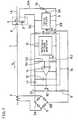
- Fig. 6is a circuit diagram of another overcurrent protection apparatus according to the prior art disclosed in the U.S. Patent No. 3,818,275.
- an electric line 1is connected to a power source line 1A of an alternating current through a switch F of a circuit breaker 2.
- the current IL of the electric line 1is detected by a current transformer 4 (hereinafter abbreviated as CT).
- CTcurrent transformer 4
- the output of the CT 4is rectified by a full wave bridge rectifier circuit 5, and a DC voltage is output from terminals 5A and 5B.
- a resistor 6 and a control circuit 7are coupled in series across the terminals 5A and 5B through a resistor 5C.
- the control circuit 7comprises two transistors 7A and 7B, which are coupled at both their collectors to the resistor 6, and a Zener diode 7C.
- the emitter of the transistor 7Ais coupled to the base of the transistor 7B through the Zener diode 7C, which is connected at its cathode to the emitter of the transistor 7A.
- the emitter of the transistor 7Bis coupled to the terminal 5B.
- Another Zener diode 8is coupled between the junction 5D between the resistors 5C and 6 and the base of the transistor 7B with the cathode of the Zener diode 8 connected to the junction 5D.
- the base of the transistor 7Ais connected to an input 7D of a timing circuit 9.
- the Zener diode 8serves to limit the voltage of the junction 5D to a predetermined voltage which is determined by the Zener voltage of the Zener diode 8.
- the timing circuit 9is coupled across the junction 5D and the terminal 5B, from which the electric power is supplied to the timing circuit 9.
- a series connection of a trip coil 3 and a thyristor 10is coupled across the junction 5D and the terminal 5B.
- the cathode of the thyristor 10is connected to the terminal 5B.
- the gate of the thyristor 10is connected to the output of the timing circuit 9.
- a capacitor Cis coupled between the junction 5D and the input 7D of the timing circuit 9.
- the current IL flowing in the electric line 1is detected by the CT 4.
- the output of the CT 4is rectified by the full wave bridge rectifier 5, and a DC voltage is output at both the terminals 5A and 5B.
- the DC voltage across the junction 5D and the terminal 5Bis lower than the Zener voltage of the Zener diode 8 and no current flows through the Zener diode 8.
- the voltage across the input 7D and the terminal 5Bis held at a constant value which is determined by the Zener voltage of the Zener diode 7C.
- the voltage across the junction 5D and the input 7Dvaries in response to the current IL of the electric line 1, since the current which flows through the resistor 6 and the control circuit 7 varies. Consequently, the electric power consumption in the resistor 6 and the control circuit 7 varies, most of the electric power in the control circuit 7 being consumed by the Zener diode 7C.
- the timing circuit 9When the current IL increases and exceeds the rated current, the voltage across the junction 5D and the input 7D exceeds a predetermined threshold voltage of the timing circuit 9, and the timing circuit 9 is activated. After a predetermined time period which is set in the timing circuit 9, the output is applied to the gate of the thyristor 10 and the thyristor 10 turns ON. Hence the trip coil 3 of the circuit breaker 2 is excited and the switch F is opened.
- An object of the present inventionis to provide an overcurrent protection apparatus which has improved electric power consumption and which can be miniaturized.
- an overcurrent protection apparatusas defined in claim 1.
- circuit diagramsare schematic representations for purposes of illustration and do not necessarily depict the actual relative sizes or locations of the elements shown.
- Fig. 1is a circuit diagram of an overcurrent protecting apparatus not part of the present invention.
- an electric line 1is connected to a power source line 1A of an alternating current through a switch F of a circuit breaker 2.
- a current IL of the electric line 1is detected by a current transformer 4.
- the output of the current transformer 4is rectified by a full wave bridge rectifier 5.
- a series connection of a transistor 15 and a resistor 6is coupled across a positive terminal 5A and a negative terminal 5B of the rectifier 5.
- a control circuit 7Ais coupled in parallel with the transistor 15.
- a timing circuit 9is coupled across a positive power source line 5C and a negative power source line 9B of the control circuit. The timing circuit 9 is activated when the absolute value of a negative input voltage V3 across the negative power source line 9B and the negative terminal 5B exceeds a predetermined voltage VT. The delay time of the timing circuit 9 varies in accordance with the negative input voltage V3.
- the timing circuit 9is provided with a filter circuit therein, and the pulsating input voltage V3 is filtered.
- the output 9A of the timing circuit 9is connected to the gate of a switch means or a thyristor 10.
- the thyristor 10turns ON when the timing circuit 9 finishes time counting operation.
- a trip coil 3 of the circuit breaker 2is connected between the positive power source line 5C and the anode of the thyristor 10, and is excited in the conductive state of the thyristor 10.
- the switch Fis disconnected by the excitation of the trip coil 3.
- a diode 11interrupts the current flow from the positive power source line 5C to the positive terminal 5A.
- a capacitor 12serves as a filter.
- a reference voltage generator 13generates a predetermined reference voltage.
- the reference voltageis applied to the invert input (-) of a comparator 14.
- the voltage V1 at the line 5Cis divided into a suitable voltage V2 by a dividing network of resistors R1 and R2.
- the voltage V2is applied to the noninvert input (+) of the comparator 14.
- the output of the comparator 14is applied to the base of the transistor 15.
- Figs. 2(a), 2(b), 2(c) and 2(d)are waveforms generated during operation.
- a current IL of the electric line 1is detected by the current transformer 4, and the output of the current transformer 4 is rectified by the rectifier 5.
- the waveform of the output current I1 from the positive terminal 5A and to the negative terminal 5B of the rectifier 5is shown in FIG. 2(a).
- the output current I1flows into the line 5C through the diode 11.
- the waveform of the voltage V2is shown in FIG. 2(b).
- the reference voltage VR of the reference voltage generator 13is shown by an alternately long- and short-dashed line.
- a voltage Vb which is lower than the voltage VRis shown by alternate long and two short dashed line.
- the voltage V2is lower than the reference voltage VR.
- the comparator 14supplies an output to the base of the transistor 15. Consequently, the transistor 15 turns ON as shown in FIG. 2(c) and the positive terminal 5A is short-circuited with the line 9B. Thereafter, the electric charge in the capacitor 12 is discharged through the comparator 14, the reference voltage generator 13, the timing circuit 9 and the resistors R1 and R2, so that the voltage V2 gradually falls.
- the output of the comparatordisappears and the transistor 15 turns OFF. Therefore, the current in the transistor 15 and the resistor 6 disappears and the voltage at the point 5A rises. The above-mentioned operation is thus repeated and the voltage V2 is limited to a voltage which is higher than the reference voltage VR. Consequently, the duty ratio of the transistor 15 is varied in accordance with the voltage across the terminals 5A and 5B.
- Fig. 3is a circuit diagram of a second circuit, also not being part of the present invention.
- the comparator 14 of the first circuitis replaced by a pulse signal generator 16.
- the remaining componentsfunction in the same manner as in the first circuit and are designated by the same reference numerals as used in Fig. 1.
- the pulse signal generator 16generates a square wave signal, the duty ratio varying in accordance with an input voltage which is applied to a terminal 16A thereof.
- the reference voltage VRis applied to the other input terminal 16B.
- Fig. 4(a)is a waveform of the output of the rectifier 5.
- Fig. 4(b)is a waveform of a voltage V1 across the lines 5C and 9B
- Fig. 4(c)is a diagram representing the switching operation of the transistor 15.
- the diagram shown in Fig. 4(c)is substantially identical to the output waveform of the pulse signal generator 16 but the cycle period of the switching operation is shorter than that of the first embodiment, and the duty ratio of the output of the pulse signal generator 16 is increased in proportion to the increase of the output voltage of the rectifier 5.
- the capacitance of the filter capacitor 12can be reduced.
- Fig. 5is a circuit diagram of an embodiment of the overcurrent protection apparatus in accordance with the present invention.
- a timing circuit 29is provided with two input terminals 29A and 29B for receiving differential inputs.
- a positive input Vcis applied across a positive power input terminal connected to the line 5C and the input terminal 29A, and a negative input Vd is applied across a negative power input terminal connected to the line 9B and the input terminal 29A.
- the input terminal 29Bis connected to the negative terminal 5B of the rectifier 5.
- Two control circuits 7B and 17are provided for supplying the positive inputs Vc and negative input Vd, respectively.
- Transistors 15 and 21are coupled to the control circuits 7B and 17, respectively.
- timing circuit 29since the timing circuit 29 is activated by the differential input, the accuracy of detection of an overcurrent is improved.
- the protection apparatus in accordance with the present inventioncan be applicable to plural electric lines.
Landscapes
- Engineering & Computer Science (AREA)
- Power Engineering (AREA)
- Emergency Protection Circuit Devices (AREA)
Description
- The present invention relates generally to overcurrent protection apparatus and, more particularly, to an overcurrent protection apparatus which includes circuit breaker means.
- The European patent application EP-A-0 130 254 discloses an overcurrent protection apparatus as specified in the preamble of
claim 1, comprising a current transformer, a rectifier for rectifying the output current of the current transformer and circuit breaker means for disconnecting the alternating current line from a power source. Switching means and a resistor are connected in series across the positive and negative outputs of the rectifier. A capacitor is coupled across the switching means through a diode for avoiding DC current flow from the capacitor to the rectifier. A reference voltage generator is provided for generating a reference voltage. The duty ratio of the switching means is controlled in proportion to the output voltage of the rectifier in an output voltage range above the reference voltage. The circuit breaker means are adapted to disconnect the AC electric line when the voltage across the resistor exceeds a predetermined value. - Fig. 6 is a circuit diagram of another overcurrent protection apparatus according to the prior art disclosed in the U.S. Patent No. 3,818,275. Referring to Fig. 6, an
electric line 1 is connected to apower source line 1A of an alternating current through a switch F of acircuit breaker 2. The current IL of theelectric line 1 is detected by a current transformer 4 (hereinafter abbreviated as CT). The output of the CT 4 is rectified by a full wavebridge rectifier circuit 5, and a DC voltage is output fromterminals - A
resistor 6 and acontrol circuit 7 are coupled in series across theterminals resistor 5C. - The
control circuit 7 comprises twotransistors resistor 6, and a Zenerdiode 7C. The emitter of thetransistor 7A is coupled to the base of thetransistor 7B through the Zenerdiode 7C, which is connected at its cathode to the emitter of thetransistor 7A. The emitter of thetransistor 7B is coupled to theterminal 5B. Another Zenerdiode 8 is coupled between thejunction 5D between theresistors transistor 7B with the cathode of the Zenerdiode 8 connected to thejunction 5D. The base of thetransistor 7A is connected to aninput 7D of atiming circuit 9. TheZener diode 8 serves to limit the voltage of thejunction 5D to a predetermined voltage which is determined by the Zener voltage of theZener diode 8. - The
timing circuit 9 is coupled across thejunction 5D and theterminal 5B, from which the electric power is supplied to thetiming circuit 9. A series connection of atrip coil 3 and athyristor 10 is coupled across thejunction 5D and theterminal 5B. The cathode of thethyristor 10 is connected to theterminal 5B. The gate of thethyristor 10 is connected to the output of thetiming circuit 9. - A capacitor C is coupled between the
junction 5D and theinput 7D of thetiming circuit 9. - In operation, the current IL flowing in the
electric line 1 is detected by the CT 4. The output of the CT 4 is rectified by the fullwave bridge rectifier 5, and a DC voltage is output at both theterminals - When the current IL is lower then a predetermined rated current, the DC voltage across the
junction 5D and theterminal 5B is lower than the Zener voltage of theZener diode 8 and no current flows through the Zenerdiode 8. A current flows through theresistor 6 and thecontrol circuit 7. The voltage across theinput 7D and theterminal 5B is held at a constant value which is determined by the Zener voltage of the Zenerdiode 7C. On the other hand, the voltage across thejunction 5D and theinput 7D varies in response to the current IL of theelectric line 1, since the current which flows through theresistor 6 and thecontrol circuit 7 varies. Consequently, the electric power consumption in theresistor 6 and thecontrol circuit 7 varies, most of the electric power in thecontrol circuit 7 being consumed by the Zenerdiode 7C. - When the current IL increases and exceeds the rated current, the voltage across the
junction 5D and theinput 7D exceeds a predetermined threshold voltage of thetiming circuit 9, and thetiming circuit 9 is activated. After a predetermined time period which is set in thetiming circuit 9, the output is applied to the gate of thethyristor 10 and thethyristor 10 turns ON. Hence thetrip coil 3 of thecircuit breaker 2 is excited and the switch F is opened. - In the
control circuit 7 of the circuit interrupter in Fig. 6, a current detected by the current transformer flows into theresistor 6 and thecontrol circuit 7, and the electric power is consumed by theresistor 6 and the Zenerdiode 7C in order to maintain the constant voltage at theinput 7D of thetiming circuit 9. Consequently, theresistor 6 and thediode 7C are heated. Thus, a heat radiator means must be provided for thecontrol circuit 7 and as a result the circuit interrupter cannot be miniaturized. - An object of the present invention is to provide an overcurrent protection apparatus which has improved electric power consumption and which can be miniaturized.
- According to the present invention there is provided an overcurrent protection apparatus as defined in
claim 1. - The present invention will now be described by way of example with reference to the accompanying drawings, in which:
- Fig. 1 is a circuit diagram of an overcurrent protection apparatus not belonging to the present invention;
- Figs. 2(a), 2(b), 2(c) and 2(d) are waveforms generated during the operation of the circuit of Fig.1;
- Fig. 3 is a circuit diagram of a second overcurrent protection apparatus not belonging to the present invention;
- Figs. 4(a), 4(b), 4(c) and 4(d) are waveforms generated during operation of the circuit of Fig.3;
- Fig. 5 is a circuit diagram of an embodiment of the present invention; and
- Fig. 6 is a circuit diagram of a prior art overcurrent protection apparatus.
- It will be recognized that the circuit diagrams are schematic representations for purposes of illustration and do not necessarily depict the actual relative sizes or locations of the elements shown.
- Fig. 1 is a circuit diagram of an overcurrent protecting apparatus not part of the present invention. With reference thereto an
electric line 1 is connected to apower source line 1A of an alternating current through a switch F of acircuit breaker 2. A current IL of theelectric line 1 is detected by a current transformer 4. The output of the current transformer 4 is rectified by a fullwave bridge rectifier 5. - A series connection of a
transistor 15 and aresistor 6 is coupled across apositive terminal 5A and anegative terminal 5B of therectifier 5. Acontrol circuit 7A is coupled in parallel with thetransistor 15. Atiming circuit 9 is coupled across a positivepower source line 5C and a negativepower source line 9B of the control circuit. Thetiming circuit 9 is activated when the absolute value of a negative input voltage V3 across the negativepower source line 9B and thenegative terminal 5B exceeds a predetermined voltage VT. The delay time of thetiming circuit 9 varies in accordance with the negative input voltage V3. Thetiming circuit 9 is provided with a filter circuit therein, and the pulsating input voltage V3 is filtered. - The
output 9A of thetiming circuit 9 is connected to the gate of a switch means or athyristor 10. Thethyristor 10 turns ON when thetiming circuit 9 finishes time counting operation. Atrip coil 3 of thecircuit breaker 2 is connected between the positivepower source line 5C and the anode of thethyristor 10, and is excited in the conductive state of thethyristor 10. The switch F is disconnected by the excitation of thetrip coil 3. Adiode 11 interrupts the current flow from the positivepower source line 5C to thepositive terminal 5A. Acapacitor 12 serves as a filter. - A
reference voltage generator 13 generates a predetermined reference voltage. The reference voltage is applied to the invert input (-) of acomparator 14. The voltage V1 at theline 5C is divided into a suitable voltage V2 by a dividing network of resistors R1 and R2. The voltage V2 is applied to the noninvert input (+) of thecomparator 14. The output of thecomparator 14 is applied to the base of thetransistor 15. - The operation of this circuit will now be described.
- Figs. 2(a), 2(b), 2(c) and 2(d) are waveforms generated during operation. A current IL of the
electric line 1 is detected by the current transformer 4, and the output of the current transformer 4 is rectified by therectifier 5. - The waveform of the output current I1 from the
positive terminal 5A and to thenegative terminal 5B of therectifier 5 is shown in FIG. 2(a). The output current I1 flows into theline 5C through thediode 11. The waveform of the voltage V2 is shown in FIG. 2(b). Referring to FIG 2(b), the reference voltage VR of thereference voltage generator 13 is shown by an alternately long- and short-dashed line. A voltage Vb which is lower than the voltage VR is shown by alternate long and two short dashed line. When a voltage V2, which is applied to thecomparator 14 at the noninvert input (+), exceeds the reference voltage VR the output of thecomparator 14 appears. Since thecomparator 14 generally has hysteresis, when the voltage which is applied to the noninvert input (+) is decreased to less than the voltage Vb, the output of thecomparator 14 disappears. - When the current IL is far lower than a predetermined rated current, the voltage V2 is lower than the reference voltage VR.
- When the current IL increases in the vicinity of the rated current and the voltage V2 exceeds the reference voltage VR, the
comparator 14 supplies an output to the base of thetransistor 15. Consequently, thetransistor 15 turns ON as shown in FIG. 2(c) and thepositive terminal 5A is short-circuited with theline 9B. Thereafter, the electric charge in thecapacitor 12 is discharged through thecomparator 14, thereference voltage generator 13, thetiming circuit 9 and the resistors R1 and R2, so that the voltage V2 gradually falls. When the voltage V2 reaches the voltage Vb, the output of the comparator disappears and thetransistor 15 turns OFF. Therefore, the current in thetransistor 15 and theresistor 6 disappears and the voltage at thepoint 5A rises. The above-mentioned operation is thus repeated and the voltage V2 is limited to a voltage which is higher than the reference voltage VR. Consequently, the duty ratio of thetransistor 15 is varied in accordance with the voltage across theterminals - Further increase of the current IL over the rated current results in an increase of the current flowing in the
resistor 6. Consequently, the absolute value of the negative voltage V3 increases as shown in Fig 2(d). When the voltage V3 exceeds the operation voltage VT of thetiming circuit 9, the time counting operation of thetiming circuit 9 is started. After a predetermined time period which is set in thetiming circuit 9, the output thereof is applied to the gate of thethyristor 10. Thus thethyristor 10 turns ON and thetrip coil 3 is excited. Hence, the switch F is opened and theelectric line 1 is disconnected from thepower source line 1A. - In this first circuit, increase of the voltage V1 is limited by short-circuiting the terminal 5A and the
line 9B from which electric power is supplied to thecontrol circuit 7A. The electric power consumption in thecontrol circuit 7 is comparatively low because the reference voltage generator and the comparator are composed of electronic components which consume little electric power. Therefore, the current flowing in theresistor 6 is comparatively lower so that the electric power consumption of theresistor 6 is comparatively lower when the terminal 5A and theline 9B are short-circuited by the conductive state of thetransistor 15. Hence, only a small size resistor is required. - Fig. 3 is a circuit diagram of a second circuit, also not being part of the present invention. In this second circuit, the
comparator 14 of the first circuit is replaced by apulse signal generator 16. The remaining components function in the same manner as in the first circuit and are designated by the same reference numerals as used in Fig. 1. Thepulse signal generator 16 generates a square wave signal, the duty ratio varying in accordance with an input voltage which is applied to a terminal 16A thereof. The reference voltage VR is applied to theother input terminal 16B. - The operation of the second circuit will now be described with reference to Figs 4(a), 4(b), 4(c) and 4(d). Fig. 4(a) is a waveform of the output of the
rectifier 5. Fig. 4(b) is a waveform of a voltage V1 across thelines transistor 15. The diagram shown in Fig. 4(c) is substantially identical to the output waveform of thepulse signal generator 16 but the cycle period of the switching operation is shorter than that of the first embodiment, and the duty ratio of the output of thepulse signal generator 16 is increased in proportion to the increase of the output voltage of therectifier 5. By means of the switching operation, even if the output of therectifier 5 increases, the voltage V1 is held to a voltage which is close to the reference voltage VR as shown in Fig. 4(b). The operation of thetiming circuit 9,thyristor 10 andcircuit breaker 2 is identical with that of the first circuit. - In the second circuit, since the cycle period of the switching operation is shorter than that of the first circuit, the capacitance of the
filter capacitor 12 can be reduced. - Fig. 5 is a circuit diagram of an embodiment of the overcurrent protection apparatus in accordance with the present invention. A
timing circuit 29 is provided with twoinput terminals line 5C and theinput terminal 29A, and a negative input Vd is applied across a negative power input terminal connected to theline 9B and theinput terminal 29A. Theinput terminal 29B is connected to thenegative terminal 5B of therectifier 5. Twocontrol circuits 7B and 17 are provided for supplying the positive inputs Vc and negative input Vd, respectively.Transistors control circuits 7B and 17, respectively. - In this embodiment, since the
timing circuit 29 is activated by the differential input, the accuracy of detection of an overcurrent is improved. - In the above-mentioned embodiment, though one of plural electric lines (for example, the three electric lines of three phase electric lines) is shown in the respective figure, the protection apparatus in accordance with the present invention can be applicable to plural electric lines.
- Although the invention has been described in a preferred form, it is to be understood that the construction, combination and arrangement of parts thereof can be changed without departing from the scope of the invention as hereinafter claimed.
Claims (1)
- An overcurrent protection apparatus comprising a current transformer (4) for detecting a current of an alternating current electric line (1), a rectifier (5) for rectifying the output current of said current transformer (4), a first switching means (15) and a resistor (6) connected in series across the positive output (5A) and the negative output (5B) of said rectifier (5), circuit breaker means (2, 10) for disconnecting said alternating current electric line (1) from an electric power source line (1A) when the voltage across said resistor (6) exceeds a predetermined value, a first capacitor (12) coupled across said first switching means (15) through a first diode means (11) for interrupting the DC current flow from said first capacitor (12) to said rectifier (5), a first reference voltage generator (13) for generating a predetermined reference voltage, and a first pulse signal generator (16) generating a signal controlling the operation of said first switching means (15) in accordance with a duty ratio which varies in proportion to the voltage across said first capacitor (12) when said voltage across said first capacitor exceeds said reference voltage,
characterized in that said protection apparatus further comprises:
a second switching means (21) connected in series with said first switching means (15) and said resistor (6) across the positive output (5A) and the negative output (5B) of said rectifier (5), a second capacitor (19) coupled across said second switching means (21) through a second diode means (18) for interrupting the DC current flow from said second capacitor (19) to said rectifier (5), a second reference voltage generator (20) for generating a predetermined second reference voltage, and a second pulse signal generator (22) generating a signal controlling the operation of said second switching means (21) in accordance with a duty ratio which varies in proportion to the voltage across said second capacitor (19) when said voltage across said second capacitor exceeds said second reference voltage.
Priority Applications (1)
| Application Number | Priority Date | Filing Date | Title |
|---|---|---|---|
| EP95113775AEP0687050A3 (en) | 1989-10-04 | 1990-09-20 | Overcurrent protection device |
Applications Claiming Priority (2)
| Application Number | Priority Date | Filing Date | Title |
|---|---|---|---|
| JP257876/89 | 1989-10-04 | ||
| JP1257876AJPH0710145B2 (en) | 1989-10-04 | 1989-10-04 | Overcurrent protection device |
Related Child Applications (1)
| Application Number | Title | Priority Date | Filing Date |
|---|---|---|---|
| EP95113775.1Division-Into | 1990-09-20 |
Publications (3)
| Publication Number | Publication Date |
|---|---|
| EP0421204A2 EP0421204A2 (en) | 1991-04-10 |
| EP0421204A3 EP0421204A3 (en) | 1992-04-08 |
| EP0421204B1true EP0421204B1 (en) | 1996-08-21 |
Family
ID=17312410
Family Applications (2)
| Application Number | Title | Priority Date | Filing Date |
|---|---|---|---|
| EP90118133AExpired - LifetimeEP0421204B1 (en) | 1989-10-04 | 1990-09-20 | An overcurrent protection apparatus |
| EP95113775AWithdrawnEP0687050A3 (en) | 1989-10-04 | 1990-09-20 | Overcurrent protection device |
Family Applications After (1)
| Application Number | Title | Priority Date | Filing Date |
|---|---|---|---|
| EP95113775AWithdrawnEP0687050A3 (en) | 1989-10-04 | 1990-09-20 | Overcurrent protection device |
Country Status (6)
| Country | Link |
|---|---|
| US (1) | US5124875A (en) |
| EP (2) | EP0421204B1 (en) |
| JP (1) | JPH0710145B2 (en) |
| KR (1) | KR910008905A (en) |
| DE (1) | DE69028171T2 (en) |
| ZA (1) | ZA906490B (en) |
Families Citing this family (24)
| Publication number | Priority date | Publication date | Assignee | Title |
|---|---|---|---|---|
| FR2699016B1 (en)* | 1992-12-04 | 1995-01-06 | Simplex Appareils | Auxiliary power supply for electrical substation. |
| DE19641185C2 (en)* | 1996-09-24 | 1998-07-23 | Siemens Ag | Circuit arrangement for current detection in current conductors for controlling electronically controllable tripping devices |
| DE19641183C2 (en)* | 1996-09-24 | 1998-08-20 | Siemens Ag | Circuit arrangement for current detection of a current conductor for controlling electronically controllable tripping devices |
| DE19641187C2 (en)* | 1996-09-24 | 1998-07-23 | Siemens Ag | Circuit arrangement for the energy supply of electronic tripping devices |
| DE19738696A1 (en)* | 1997-08-29 | 1999-03-04 | Siemens Ag | Circuit arrangement for feeding a tripping magnet of a circuit breaker |
| JP2003050637A (en)* | 2001-08-07 | 2003-02-21 | Mitsubishi Electric Corp | Power supply |
| US6813124B1 (en) | 2002-06-21 | 2004-11-02 | Lionel L.L.C. | Transformer over-current protection with RMS sensing and voltage fold-back |
| AU2002950581A0 (en)* | 2002-08-02 | 2002-09-12 | Wayne Callen | Electrical safety circuit |
| US7561396B2 (en)* | 2004-03-09 | 2009-07-14 | Samsung Measuring Instruments Co., LTD | Apparatus for monitoring open state of the secondary terminals of a current transformer |
| DE102005031833B4 (en)* | 2005-07-06 | 2017-01-05 | Phoenix Contact Gmbh & Co. Kg | Method and electronic power supply device for supplying power to a low-voltage load protected by a protective device |
| CN101507060B (en)* | 2006-06-30 | 2011-08-10 | 莫列斯公司 | Low profile latching connector and pull tab for unlatching same |
| US7869170B2 (en)* | 2006-07-14 | 2011-01-11 | Susan Jean Walker Colsch | Method and system for time synchronized trip algorithms for breaker self protection |
| US7791849B2 (en)* | 2006-07-14 | 2010-09-07 | William Davison | Redundant trip activation |
| US7697250B2 (en)* | 2006-07-14 | 2010-04-13 | William Davison | Switch-to-trip point translation |
| US8154373B2 (en)* | 2006-07-14 | 2012-04-10 | Schneider Electric USA, Inc. | Circuit breaker-like apparatus with combination current transformer |
| US7683586B2 (en)* | 2006-07-14 | 2010-03-23 | Davison William C | Method and system of fault powered supply voltage regulation |
| US7869169B2 (en)* | 2006-07-14 | 2011-01-11 | William Davison | Method and system of current transformer output magnitude compensation in a circuit breaker system |
| US7788055B2 (en) | 2006-07-14 | 2010-08-31 | Square D Company | Method and system of calibrating sensing components in a circuit breaker system |
| US7592888B2 (en)* | 2006-07-14 | 2009-09-22 | Jason Robert Colsch | Low cost user adjustment, resistance to straying between positions, increased resistance to ESD, and consistent feel |
| US7859802B2 (en)* | 2006-07-14 | 2010-12-28 | William Davison | Burden resistor temperature compensation algorithm |
| US7550939B2 (en)* | 2006-07-14 | 2009-06-23 | William Davison | Redundant instantaneous trip detection |
| CN106026656B (en)* | 2016-07-08 | 2019-01-25 | 上海电科电器科技有限公司 | Sluggish type power circuit |
| CN107528291A (en)* | 2017-09-28 | 2017-12-29 | 苏州威利仕塑胶电子有限公司 | One kind crosses undercurrent controller |
| US10811185B2 (en) | 2018-09-13 | 2020-10-20 | Analog Devices Global Unlimited Company | Saturation prevention of current transformer |
Family Cites Families (8)
| Publication number | Priority date | Publication date | Assignee | Title |
|---|---|---|---|---|
| FR2052906B2 (en)* | 1969-06-20 | 1975-08-22 | Comp Generale Electricite | |
| US3846675A (en)* | 1973-01-30 | 1974-11-05 | Westinghouse Electric Corp | Molded case circuit breakers utilizing saturating current transformers |
| US3818275A (en)* | 1973-01-30 | 1974-06-18 | Westinghouse Electric Corp | Circuit interrupter including improved trip circuit using current transformers |
| CH558098A (en)* | 1973-11-27 | 1975-01-15 | Sprecher & Schuh Ag | CIRCUIT ARRANGEMENT FOR POWERING ELECTRONIC PROTECTIVE RELAY. |
| US4351012A (en)* | 1980-04-15 | 1982-09-21 | Westinghouse Electric Corp. | Circuit interrupter with digital trip unit and means to enter trip settings |
| US4331999A (en)* | 1980-04-15 | 1982-05-25 | Westinghouse Electric Corp. | Circuit interrupter with digital trip unit and power supply |
| US4567540A (en)* | 1983-06-22 | 1986-01-28 | S&C Electric Company | Power supply for a circuit interrupter |
| US4603336A (en)* | 1984-04-25 | 1986-07-29 | Harris Graphics Corporation | Transfer mechanism for multiple station imaging/printing apparatus |
- 1989
- 1989-10-04JPJP1257876Apatent/JPH0710145B2/ennot_activeExpired - Lifetime
- 1990
- 1990-07-23KRKR1019900011162Apatent/KR910008905A/ennot_activeWithdrawn
- 1990-08-16ZAZA906490Apatent/ZA906490B/enunknown
- 1990-08-17USUS07/568,863patent/US5124875A/ennot_activeExpired - Fee Related
- 1990-09-20EPEP90118133Apatent/EP0421204B1/ennot_activeExpired - Lifetime
- 1990-09-20DEDE69028171Tpatent/DE69028171T2/ennot_activeExpired - Lifetime
- 1990-09-20EPEP95113775Apatent/EP0687050A3/ennot_activeWithdrawn
Also Published As
| Publication number | Publication date |
|---|---|
| EP0421204A3 (en) | 1992-04-08 |
| KR910008905A (en) | 1991-05-31 |
| EP0687050A3 (en) | 1996-05-22 |
| JPH0710145B2 (en) | 1995-02-01 |
| DE69028171D1 (en) | 1996-09-26 |
| ZA906490B (en) | 1991-06-26 |
| JPH03124215A (en) | 1991-05-27 |
| US5124875A (en) | 1992-06-23 |
| EP0421204A2 (en) | 1991-04-10 |
| EP0687050A2 (en) | 1995-12-13 |
| DE69028171T2 (en) | 1997-01-23 |
Similar Documents
| Publication | Publication Date | Title |
|---|---|---|
| EP0421204B1 (en) | An overcurrent protection apparatus | |
| US5808847A (en) | Electronic trip device comprising a power supply device | |
| EP0108279B1 (en) | High-voltage dc circuit breaker apparatus | |
| EP0188839B1 (en) | Self-oscillating power-supply circuit | |
| JP3349781B2 (en) | Switching regulator power supply | |
| US5978243A (en) | Ac/dc converting circuit | |
| US4882663A (en) | MOSFET flyback converter | |
| KR960003201B1 (en) | Abnormal voltage detection control device | |
| JPH06225172A (en) | Switching mode power supply | |
| KR920011020A (en) | Simple low noise low power dual mode battery charging circuit | |
| HK92196A (en) | Electronic switch supply unit | |
| JP3335838B2 (en) | Circuit breaker | |
| EP1639695B1 (en) | Switch mode power circuit | |
| EP0060519A2 (en) | Power source device | |
| JPH08221141A (en) | Power supply circuit | |
| EP0004462A1 (en) | AC control apparatus | |
| JPS6377383A (en) | Starting circuit | |
| JPS58364Y2 (en) | Tripping circuit for circuit breakers | |
| JP2941513B2 (en) | Undervoltage trip device | |
| JP3281052B2 (en) | Power circuit | |
| JPH07163142A (en) | Switching power supply | |
| JP2720895B2 (en) | Ringing choke converter control circuit | |
| JPH0370208A (en) | Zero cross contactless switch | |
| JPH05316723A (en) | Switching power supply | |
| SU1019542A1 (en) | Device for overload protection of power supply source |
Legal Events
| Date | Code | Title | Description |
|---|---|---|---|
| PUAI | Public reference made under article 153(3) epc to a published international application that has entered the european phase | Free format text:ORIGINAL CODE: 0009012 | |
| 17P | Request for examination filed | Effective date:19900920 | |
| AK | Designated contracting states | Kind code of ref document:A2 Designated state(s):CH DE FR GB IT LI | |
| PUAL | Search report despatched | Free format text:ORIGINAL CODE: 0009013 | |
| AK | Designated contracting states | Kind code of ref document:A3 Designated state(s):CH DE FR GB IT LI | |
| 17Q | First examination report despatched | Effective date:19931227 | |
| GRAH | Despatch of communication of intention to grant a patent | Free format text:ORIGINAL CODE: EPIDOS IGRA | |
| GRAH | Despatch of communication of intention to grant a patent | Free format text:ORIGINAL CODE: EPIDOS IGRA | |
| GRAA | (expected) grant | Free format text:ORIGINAL CODE: 0009210 | |
| AK | Designated contracting states | Kind code of ref document:B1 Designated state(s):CH DE FR GB IT LI | |
| XX | Miscellaneous (additional remarks) | Free format text:TEILANMELDUNG 95113775.1 EINGEREICHT AM 01/09/95. | |
| REG | Reference to a national code | Ref country code:CH Ref legal event code:NV Representative=s name:BOVARD AG PATENTANWAELTE | |
| REF | Corresponds to: | Ref document number:69028171 Country of ref document:DE Date of ref document:19960926 | |
| ET | Fr: translation filed | ||
| ITF | It: translation for a ep patent filed | ||
| PLBE | No opposition filed within time limit | Free format text:ORIGINAL CODE: 0009261 | |
| STAA | Information on the status of an ep patent application or granted ep patent | Free format text:STATUS: NO OPPOSITION FILED WITHIN TIME LIMIT | |
| 26N | No opposition filed | ||
| PGFP | Annual fee paid to national office [announced via postgrant information from national office to epo] | Ref country code:CH Payment date:19981009 Year of fee payment:9 | |
| ITPR | It: changes in ownership of a european patent | Owner name:OFFERTA DI LICENZA AL PUBBLICO;AL PUBBLICO | |
| REG | Reference to a national code | Ref country code:GB Ref legal event code:746 Effective date:19990519 | |
| PG25 | Lapsed in a contracting state [announced via postgrant information from national office to epo] | Ref country code:CH Free format text:LAPSE BECAUSE OF NON-PAYMENT OF DUE FEES Effective date:19990930 Ref country code:LI Free format text:LAPSE BECAUSE OF NON-PAYMENT OF DUE FEES Effective date:19990930 | |
| REG | Reference to a national code | Ref country code:FR Ref legal event code:D6 | |
| REG | Reference to a national code | Ref country code:CH Ref legal event code:PL | |
| REG | Reference to a national code | Ref country code:GB Ref legal event code:IF02 | |
| PG25 | Lapsed in a contracting state [announced via postgrant information from national office to epo] | Ref country code:IT Free format text:LAPSE BECAUSE OF NON-PAYMENT OF DUE FEES;WARNING: LAPSES OF ITALIAN PATENTS WITH EFFECTIVE DATE BEFORE 2007 MAY HAVE OCCURRED AT ANY TIME BEFORE 2007. THE CORRECT EFFECTIVE DATE MAY BE DIFFERENT FROM THE ONE RECORDED. Effective date:20050920 | |
| PGFP | Annual fee paid to national office [announced via postgrant information from national office to epo] | Ref country code:GB Payment date:20090916 Year of fee payment:20 | |
| PGFP | Annual fee paid to national office [announced via postgrant information from national office to epo] | Ref country code:DE Payment date:20090917 Year of fee payment:20 | |
| PGFP | Annual fee paid to national office [announced via postgrant information from national office to epo] | Ref country code:FR Payment date:20091012 Year of fee payment:20 | |
| REG | Reference to a national code | Ref country code:GB Ref legal event code:PE20 Expiry date:20100919 | |
| PG25 | Lapsed in a contracting state [announced via postgrant information from national office to epo] | Ref country code:GB Free format text:LAPSE BECAUSE OF EXPIRATION OF PROTECTION Effective date:20100919 | |
| PG25 | Lapsed in a contracting state [announced via postgrant information from national office to epo] | Ref country code:DE Free format text:LAPSE BECAUSE OF EXPIRATION OF PROTECTION Effective date:20100920 |