EP0419093B1 - Current sensing circuit - Google Patents
Current sensing circuitDownload PDFInfo
- Publication number
- EP0419093B1 EP0419093B1EP90309740AEP90309740AEP0419093B1EP 0419093 B1EP0419093 B1EP 0419093B1EP 90309740 AEP90309740 AEP 90309740AEP 90309740 AEP90309740 AEP 90309740AEP 0419093 B1EP0419093 B1EP 0419093B1
- Authority
- EP
- European Patent Office
- Prior art keywords
- mos transistor
- circuit
- source
- voltage
- load
- Prior art date
- Legal status (The legal status is an assumption and is not a legal conclusion. Google has not performed a legal analysis and makes no representation as to the accuracy of the status listed.)
- Expired - Lifetime
Links
- 230000003111delayed effectEffects0.000claimsdescription3
- 238000010586diagramMethods0.000description10
- 230000004913activationEffects0.000description2
- 230000006378damageEffects0.000description1
- 230000005669field effectEffects0.000description1
- 230000001052transient effectEffects0.000description1
Images


Classifications
- G—PHYSICS
- G01—MEASURING; TESTING
- G01R—MEASURING ELECTRIC VARIABLES; MEASURING MAGNETIC VARIABLES
- G01R15/00—Details of measuring arrangements of the types provided for in groups G01R17/00 - G01R29/00, G01R33/00 - G01R33/26 or G01R35/00
- G—PHYSICS
- G01—MEASURING; TESTING
- G01R—MEASURING ELECTRIC VARIABLES; MEASURING MAGNETIC VARIABLES
- G01R19/00—Arrangements for measuring currents or voltages or for indicating presence or sign thereof
- G01R19/165—Indicating that current or voltage is either above or below a predetermined value or within or outside a predetermined range of values
- G01R19/16504—Indicating that current or voltage is either above or below a predetermined value or within or outside a predetermined range of values characterised by the components employed
- G01R19/16519—Indicating that current or voltage is either above or below a predetermined value or within or outside a predetermined range of values characterised by the components employed using FET's
- G—PHYSICS
- G01—MEASURING; TESTING
- G01R—MEASURING ELECTRIC VARIABLES; MEASURING MAGNETIC VARIABLES
- G01R19/00—Arrangements for measuring currents or voltages or for indicating presence or sign thereof
- G01R19/165—Indicating that current or voltage is either above or below a predetermined value or within or outside a predetermined range of values
Definitions
- This inventionconcerns a current sensing circuit using FET (Field Effect Transistor). More particularly, this invention concerns a current sensing circuit which is used as an over current sensing circuit in a power circuit.
- FETField Effect Transistor
- a current sensing circuitwhich includes a resistor connected in series with the load is often used.
- the load currentis sensed by sensing the voltage drop at the resistor.
- the power consumptionis increased.
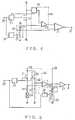
- FIG.1shows a circuit diagram of the current sensing circuit disclosed in the United States Patent.
- a main FET 1is connected in series with a load 4 between a first power source terminal 6 and a second power source terminal 7 .
- a sense FET 2is connected in parallel with the main FET 1. This connection allows a second current path for part of the load current which flows through the load 4.
- a comparator 8compares the voltage drop at a resistor 5 with a reference voltage supplied to a terminal 7, and produces an output signal from an output terminal 10 in accordance with the comparison result.
- US-A-4082968discloses a current sensing circuit for sensing a load current flowing through the load.
- the current sensing circuithas a first MOS transistor having a source to drain path connected in series with the load and having a gate electrode.
- the first MOS transistorproduces a source to drain voltage in response to the load current.
- An input terminalis supplied with an input signal, the first MOS transistor being responsive to the input signal.
- Reference voltage generating meansinclude a second MOS transistor and a constant current source connected to the second MOS transistor for generating a reference voltage.
- An object of the present inventionis to provide a sensing circuit which has a low power consumption and a high sensing accuracy.
- FIG.2is a circuit diagram of a first embodiment of the present invention.
- numerals 29 and 30designate power source terminals
- numeral 28designates an input terminal.
- a first MOS transistor 21there is provided a first MOS transistor 21 .
- the source to drain path of the MOS transistor 21is connected in series with a load 24 .
- Numeral 23designates a drive circuit, e.g., composed of CMOS circuits, which provides a drive signal to the gate electrode of the first MOS transistor 21 in response to an input signal supplied to the input terminal 28 .
- the reference voltage generating means 20comprises a second MOS transistor 22 and a constant current source 25 .
- the constant current source 25provides a predetermined current I o to the MOS transistor 22 responsive to a power source voltage supplied to the power source terminal 30 .
- the present embodimentis further provided with delay means 26 , e.g., composed of a conventional CR circuit.
- the delay means 26supplies a delayed input signal to the gate electrode of the second MOS transistor 22 .
- the embodimentis provided with first circuit means 40 .
- the first circuit means 40includes bipolar transistors 42 and 43 , and resistors 44 and 45 .
- the first circuit means 40further includes a MOS transistor 41 .
- the emitter electrodes of the transistors 42 and 43are connected to the drain electrode of the first MOS transistor 21 , and the base electrodes thereof are connected in common.
- the collector electrodes of the transistors 42 and 43are connected to the resistors 44 and 45 , respectively. In this way, the transistors 42 and 43 form a current mirror circuit.
- the emitter area ratio between the transistors 42 and 43is n (n is larger than 1).
- the gate electrode of the MOS transistor 41is connected to the gate electrode of the first MOS transistor 21 , and the drain electrode thereof is connected to the resistor 44 .
- the present embodimentis still further provided a comparing means 27 , e.g., composed of a comparator circuit.
- the comparing means 27includes first and second input terminals, and the first input terminal is connected to the collector electrode of the transistor 43 and the other is connected to the drain electrode of the transistor 22 to receive the reference voltage Vr.
- the sensing circuitwhen an input signal (not shown) is supplied to the input terminal 28 at timing T o, the drive circuit 23 provides a drive signal to the gate electrodes of the MOS transistor 21 and 41 . In response to the drive signal, the transistors 21 and 41 are switched to the ON state. Assuming that the emitter to collector voltage of transistor 43 is negligible, the collector voltage Vs of transistor 43 is substantially equal to the drain voltage V1 of the MOS transistor 21 . Thus, the source to drain voltage of the transistor 21 is transferred, and is supplied to the comparing means 27 .
- the load current I outis sensed by comparing the voltage Vs with the reference voltage Vr. Namely, for example, when the voltage Vs is higher than the reference voltage Vr, the comparing means 27 produces a high level output signal, and when the voltage Vs is lower than the reference voltage Vr, produces a low level output signal. Therefore, by discriminating whether the output of the comparating means 27 is high level or low level, it can be sensed whether the load current I out is greater than the predetermined current I o, or within an allowed operating area.
- the constant current I ocan be set arbitrarily to determine a predetermined load current limit, and the relationship between the load current Iout and the constant surrent I o is explained as follows.
- I out .R1I o.
- R2 I out( R2 / R1 ) .I o wherein R1 is a ON resistance of the transistor 21 and R2 is the ON resistance of the transistor 22 .
- the source to drain voltage of the first MOS transistor 21is compared with the reference voltage Vr, which is established by the source to drain voltage of the second MOS transistor 22 .
- Vrthe reference voltage
- the voltages which are to be comparedhave the same temperature coefficient.
- the temperature coefficientscompensate each other, and the sensing accuracy is improved over a range of temperatures.
- the activation of the transistor 22is delayed by T d due to the delay means 26 .
- the transient period illustrated by circle Ais excluded from the sensing. Therefore, even if there exists a time lag between the activation of the transistor 21 and the transfer of the voltage V1 to the collector electrode of the transistor 43 , erroneous sensing can be prevented.
- the source to drain voltage of the transistor 21is only supplied to the sensing means 27 when the transistor 41 is in the ON state.
- a relatively low voltageis supplied to the sensing means 27 . Therefore, it is possible to prevent a high voltage supply to the sensing means 27 , and thus to prevent destruction due to a high voltage supply.
- FIG.4is a circuit diagram of a second embodiment of the present invention.
- first circuit means 40which produces an output voltage which is proportional to the source to drain voltage of the first MOS transistor 21 .
- the first circuit means 40includes a switching circuit 50 and an amplifier circuit 53 .
- the switching circuit 50is supplied with an output signal from the drive circuit 23 and is controlled by the signal.
- the amplifier circuit 53is supplied with the output of the switching circuit 50 and the source voltage of the transistor 21 .
- the drive circuit 23when an input signal is supplied to the input terminal 28 , the drive circuit 23 produces a drive signal to the gate electrode of the transistor 21 and the switching circuit 50 . In response to the drive signal, the switching circuit 50 switches to the ON state, and transfers the drain voltage of the MOS transistor 21 to the amplifier circuit 53 .
- the input voltage to the amplifier circuit 53is substantially equal to the source to drain voltage of the transistor 21 , and the amplifier circuit 53 produces an output which is proportional to the source to drain voltage of the MOS transistor 21 .
- the output of the amplifier circuit 53is compared with the reference voltage Vr from the reference voltage generating means 20 by the comparing means 27 .
- FIG.5is a circuit diagram of a third embodiment of the present invention. In this circuit, the switching circuit 50 in FIG.4 is illustrated concretely.
- the switching circuit 50includes a MOS transistor 52 and a resistor 51 .
- the gate electrode of the transistor 52is connected to the output of the drive circuit 23 , and the source electrode thereof is connected to the input of the amplifier circuit 53 .
- the transistor 52switches to the ON state in response to an output signal from the drive circuit 23 .
- the ON resistance of the transistor 52is substantially equal to the drain voltage of the transistor 21 .
- the input voltage to the amplifier circuit 53is substantially equal to the source to drain voltage of the transistor 21 . Therefore, the output of the amplifier 53 is proportional to the source to drain voltage of the MOS transistor 21 .
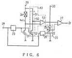
- FIG.6is a circuit diagram of a fourth embodiment of the present invention.
- the location of the load 24 and the MOS transistor 21 in FIG.5is changed with respect to the power supply. Namely, the drain electrode of the transistor 21 is connected to the load 24 , and the source electrode thereof is connected to the ground.
- the gate electrode of the transistor 52is connected to the gate electrode of the transistor 21 , and the drain electrode thereof is connected to the power supply terminal 29 through a resistor 51 .
- the input terminals of the amplifier circuit 53are supplied with the drain voltages of the MOS transistors 21 and 52 . Assuming that the source to drain voltage of the transistor 52 is negligible, the input to the amplifier circuit 53 is substantially equal to the source to drain voltage of the transistor 21 . Thus, similarly to the third embodiment in FIG.5 , the amplifier circuit 53 outputs an voltage which is proportional to the source to drain voltage of the MOS transistor 21 . Thus, by comparing the output of the amplifier circuit 53 and the reference voltage Vr, the load current Iout can be sensed.
- a comparator circuitis used as the comparing means 27 .
- an operational amplifieras the comparing means 27 .
- an analogous detecting of the load current Ioutcan be achieved. Namely, by converting the output voltage of the operational amplifier to a current using a voltage to current converter circuit (not shown), a concrete value of the load current Iout can be achieved.
Landscapes
- Physics & Mathematics (AREA)
- General Physics & Mathematics (AREA)
- Measurement Of Current Or Voltage (AREA)
- Control Of Voltage And Current In General (AREA)
Description
- This invention concerns a current sensing circuit using FET (Field Effect Transistor). More particularly, this invention concerns a current sensing circuit which is used as an over current sensing circuit in a power circuit.
- It is often desirable to sense a load current in order to either control that current or to prevent it from exceeding certain bounds. Conventionally, a current sensing circuit which includes a resistor connected in series with the load is often used. In this circuit, the load current is sensed by sensing the voltage drop at the resistor. However, by inserting a resistor in a high current path, the power consumption is increased.
- Thus, to reduce the power consumption, a current sensing circuit using a main FET and a sense FET is disclosed in US-A-4,553,084.
- FIG.1 shows a circuit diagram of the current sensing circuit disclosed in the United States Patent. In the current sensing circuit, a
main FET 1 is connected in series with aload 4 between a firstpower source terminal 6 and a secondpower source terminal 7. A sense FET2 is connected in parallel with themain FET 1. This connection allows a second current path for part of the load current which flows through theload 4. A comparator 8 compares the voltage drop at a resistor 5 with a reference voltage supplied to aterminal 7, and produces an output signal from anoutput terminal 10 in accordance with the comparison result. - In this circuit, a small resistance is required for the sense resistor 5 to keep good linearity of the current which flows through resistor 5 with respect to the load current. Namely, the accuracy of the resistor 5 determines the accuracy of the sensing. However, it is not so easy to provide a resistor with an accurate but small resistance value.
- US-A-4082968 discloses a current sensing circuit for sensing a load current flowing through the load. The current sensing circuit has a first MOS transistor having a source to drain path connected in series with the load and having a gate electrode. The first MOS transistor produces a source to drain voltage in response to the load current. An input terminal is supplied with an input signal, the first MOS transistor being responsive to the input signal. Reference voltage generating means include a second MOS transistor and a constant current source connected to the second MOS transistor for generating a reference voltage.
- An object of the present invention is to provide a sensing circuit which has a low power consumption and a high sensing accuracy.
- According to the present invention, there is provided a current sensing circuit for sensing a load current flowing through a load comprising: a first MOS transistor having a source to drain path connected in series with said load and having a gate electrode, said first MOS transistor producing a source to drain voltage in response to the load current; an input terminal supplied with an input signal, the first MOS transistor being responsive to said input signal; reference voltage generating means including a second MOS transistor and a constant current source connected to the second MOS transistor, for generating a reference voltage; characterized in that it further comprises first circuit means for producing an output voltage which is proportional to the source to drain voltage of the first MOS transistor; and comparing means for comparing the output voltage of the first circuit means with the reference voltage.
- The accompanying drawings, which are incorporated in and constitute a part of the specification, illustrate an embodiment of the invention, and, together with the description, serve to explain the principles of the invention. Referring now to the drawings, like reference characters designate like or corresponding parts throughout the several views. In the drawings:
- FIG. 1 is a circuit diagram of a conventional sensing circuit;
- FIG. 2 is a circuit diagram of a first embodiment of the present invention;
- FIG. 3 is a timing chart to explain the operation of the circuit in FIG. 2;
- FIG. 4 is a circuit diagram of a second embodiment of the present invention;
- FIG. 5 is a circuit diagram of a third embodiment of the present invention;
- FIG.6 is a circuit diagram of a fourth embodiment of the present invention.
- Referring now to the drawings, the present invention will be explained.FIG.2 is a circuit diagram of a first embodiment of the present invention. In the drawing,
numerals numeral 28 designates an input terminal. - In this embodiment, there is provided a
first MOS transistor 21. The source to drain path of theMOS transistor 21 is connected in series with aload 24. - Numeral23 designates a drive circuit, e.g., composed of CMOS circuits, which provides a drive signal to the gate electrode of the
first MOS transistor 21 in response to an input signal supplied to theinput terminal 28. - Furthermore, in the present embodiment, there is provided a reference voltage generating means20. The reference voltage generating means20 comprises a
second MOS transistor 22 and a constantcurrent source 25. The constantcurrent source 25 provides a predetermined currentIo to theMOS transistor 22 responsive to a power source voltage supplied to thepower source terminal 30. - The present embodiment is further provided with delay means26, e.g., composed of a conventional CR circuit. The delay means26 supplies a delayed input signal to the gate electrode of the
second MOS transistor 22. - Furthermore, the embodiment is provided with first circuit means40. The first circuit means40 includes
bipolar transistors transistors first MOS transistor 21, and the base electrodes thereof are connected in common. The collector electrodes of thetransistors transistors transistors - The gate electrode of the MOS transistor41 is connected to the gate electrode of the
first MOS transistor 21, and the drain electrode thereof is connected to the resistor44. - The present embodiment is still further provided a
comparing means 27, e.g., composed of a comparator circuit. The comparing means27 includes first and second input terminals, and the first input terminal is connected to the collector electrode of thetransistor 43 and the other is connected to the drain electrode of thetransistor 22 to receive the reference voltage Vr. - The operation of the sensing circuit will be explained using a timing chart illustrated inFIG.3. In this sensing circuit, when an input signal (not shown) is supplied to the
input terminal 28 at timingTo, thedrive circuit 23 provides a drive signal to the gate electrodes of theMOS transistor 21 and41. In response to the drive signal, thetransistors 21 and41 are switched to the ON state. Assuming that the emitter to collector voltage oftransistor 43 is negligible, the collector voltage Vs oftransistor 43 is substantially equal to the drain voltage V1 of theMOS transistor 21. Thus, the source to drain voltage of thetransistor 21 is transferred, and is supplied to thecomparing means 27. - In this embodiment, the load currentIout is sensed by comparing the voltage Vs with the reference voltage Vr. Namely, for example, when the voltage Vs is higher than the reference voltage Vr, the comparing means27 produces a high level output signal, and when the voltage Vs is lower than the reference voltage Vr, produces a low level output signal. Therefore, by discriminating whether the output of the comparating
means 27 is high level or low level, it can be sensed whether the load currentIout is greater than the predetermined currentIo, or within an allowed operating area. - The constant currentIo can be set arbitrarily to determine a predetermined load current limit, and the relationship between the load current Iout and the constant surrentIo is explained as follows.


whereinR1 is a ON resistance of thetransistor 21 andR2 is the ON resistance of thetransistor 22. - According to the present invention, the source to drain voltage of the
first MOS transistor 21 is compared with the reference voltage Vr, which is established by the source to drain voltage of thesecond MOS transistor 22. Thus, the voltages which are to be compared have the same temperature coefficient. Thus, the temperature coefficients compensate each other, and the sensing accuracy is improved over a range of temperatures. - As shown inFIG.3(b), the activation of the
transistor 22 is delayed byTd due to the delay means26. Thus, the transient period illustrated by circleA is excluded from the sensing. Therefore, even if there exists a time lag between the activation of thetransistor 21 and the transfer of the voltage V1 to the collector electrode of thetransistor 43, erroneous sensing can be prevented. - Furthermore, in this embodiment, the source to drain voltage of the
transistor 21 is only supplied to the sensing means27 when the transistor41 is in the ON state. Thus, only a relatively low voltage is supplied to the sensing means27. Therefore, it is possible to prevent a high voltage supply to the sensing means27, and thus to prevent destruction due to a high voltage supply. - FIG.4 is a circuit diagram of a second embodiment of the present invention. In this embodiment, there is provided first circuit means40 which produces an output voltage which is proportional to the source to drain voltage of the
first MOS transistor 21. - The first circuit means40 includes a switching
circuit 50 and anamplifier circuit 53. The switchingcircuit 50 is supplied with an output signal from thedrive circuit 23 and is controlled by the signal. Theamplifier circuit 53 is supplied with the output of the switchingcircuit 50 and the source voltage of thetransistor 21. - In this circuit, when an input signal is supplied to the
input terminal 28, thedrive circuit 23 produces a drive signal to the gate electrode of thetransistor 21 and the switchingcircuit 50. In response to the drive signal, the switchingcircuit 50 switches to the ON state, and transfers the drain voltage of theMOS transistor 21 to theamplifier circuit 53. - Therefore, the input voltage to the
amplifier circuit 53 is substantially equal to the source to drain voltage of thetransistor 21, and theamplifier circuit 53 produces an output which is proportional to the source to drain voltage of theMOS transistor 21. The output of theamplifier circuit 53 is compared with the reference voltage Vr from the reference voltage generating means20 by the comparingmeans 27. - FIG.5 is a circuit diagram of a third embodiment of the present invention. In this circuit, the switching
circuit 50 inFIG.4 is illustrated concretely. - Namely, the switching
circuit 50 includes a MOS transistor52 and aresistor 51. The gate electrode of the transistor52 is connected to the output of thedrive circuit 23, and the source electrode thereof is connected to the input of theamplifier circuit 53. - In this circuit, the transistor52 switches to the ON state in response to an output signal from the
drive circuit 23. By setting the ON resistance of the transistor52 to be negligible with respect to the resistance value of theresistor 51, the source voltage of the transistor52 is substantially equal to the drain voltage of thetransistor 21. Thus, the input voltage to theamplifier circuit 53 is substantially equal to the source to drain voltage of thetransistor 21. Therefore, the output of theamplifier 53 is proportional to the source to drain voltage of theMOS transistor 21. Thus, by comparing the output of theamplifier circuit 53 with the reference voltage, it is possible to sense the load current Iout. - FIG.6 is a circuit diagram of a fourth embodiment of the present invention. In this embodiment, the location of the
load 24 and theMOS transistor 21 inFIG.5 is changed with respect to the power supply. Namely, the drain electrode of thetransistor 21 is connected to theload 24, and the source electrode thereof is connected to the ground. The gate electrode of the transistor52 is connected to the gate electrode of thetransistor 21, and the drain electrode thereof is connected to thepower supply terminal 29 through aresistor 51. - The input terminals of the
amplifier circuit 53 are supplied with the drain voltages of theMOS transistors 21 and52. Assuming that the source to drain voltage of the transistor52 is negligible, the input to theamplifier circuit 53 is substantially equal to the source to drain voltage of thetransistor 21. Thus, similarly to the third embodiment inFIG.5, theamplifier circuit 53 outputs an voltage which is proportional to the source to drain voltage of theMOS transistor 21. Thus, by comparing the output of theamplifier circuit 53 and the reference voltage Vr, the load current Iout can be sensed. - In the above mentioned embodiments, a comparator circuit is used as the comparing
means 27. However, by using an operational amplifier as the comparingmeans 27, an analogous detecting of the load current Iout can be achieved. Namely, by converting the output voltage of the operational amplifier to a current using a voltage to current converter circuit (not shown), a concrete value of the load current Iout can be achieved.


Claims (5)
- A current sensing circuit for sensing a load current flowing through a load (24) comprising:
a first MOS transistor (21) having a source to drain path connected in series with said load and having a gate electrode, said first MOS transistor (21) producing a source to drain voltage in response to the load current;
an input terminal (28) supplied with an input signal, the first MOS transistor (21) being responsive to said input signal; and
reference voltage generating means (20) including a second MOS transistor (22) and a constant current source (25) connected to the second MOS transistor, for generating a reference voltage (Vr);
characterized in that it further comprises
first circuit means (40) for producing an output voltage which is proportional to the source to drain voltage of the first MOS transistor (21); and
comparing means (27) for comparing the output voltage of the first circuit means (40) with the reference voltage (Vr). - The current sensing circuit of claim 1, further comprising a delay means (26), and wherein the second MOS transistor (22) is supplied with a delayed input signal through the delay means (22).
- The current sensing circuit of claim 1, wherein the first circuit means (40) includes a third MOS transistor (41,52) having a gate electrode connected to the gate electrode of the first MOS transistor, wherein said first circuit means provides the output voltage to the comparing means in response to the input signal.
- The current sensing circuit of claim 1, wherein the first circuit means (40) includes a serial connection of a third MOS transistor (52) and a resistor (51) being arranged in parallel with respect to the connection of the load (24) and the first MOS transistor (21), the first and the second MOS transistors each having a source electrode, a drain electrode and a gate electrode, and an amplifier circuit (53) having input terminals connected to the source electrodes of the first and the third MOS transistors.
- The current sensing circuit of claim 1, wherein the first circuit means (40) includes a serial connection of a third MOS transistor (52) and a resistor (51) being arranged in parallel with respect to the connection of the load (24) and the first MOS transistor (21), the first and the second MOS transistors each having a source electrode, a drain electrode and a gate electrode, and an amplifier circuit (53) having input terminals connected to the drain electrodes of the first and the third MOS transistors.
Applications Claiming Priority (2)
| Application Number | Priority Date | Filing Date | Title |
|---|---|---|---|
| JP1242024AJPH079442B2 (en) | 1989-09-20 | 1989-09-20 | Current detection circuit |
| JP242024/89 | 1989-09-20 |
Publications (3)
| Publication Number | Publication Date |
|---|---|
| EP0419093A2 EP0419093A2 (en) | 1991-03-27 |
| EP0419093A3 EP0419093A3 (en) | 1991-06-19 |
| EP0419093B1true EP0419093B1 (en) | 1994-01-05 |
Family
ID=17083136
Family Applications (1)
| Application Number | Title | Priority Date | Filing Date |
|---|---|---|---|
| EP90309740AExpired - LifetimeEP0419093B1 (en) | 1989-09-20 | 1990-09-05 | Current sensing circuit |
Country Status (5)
| Country | Link |
|---|---|
| US (1) | US5113089A (en) |
| EP (1) | EP0419093B1 (en) |
| JP (1) | JPH079442B2 (en) |
| KR (1) | KR930007482B1 (en) |
| DE (1) | DE69005755T2 (en) |
Cited By (16)
| Publication number | Priority date | Publication date | Assignee | Title |
|---|---|---|---|---|
| DE19838657B4 (en)* | 1998-08-25 | 2008-01-24 | Infineon Technologies Ag | Circuit arrangement for detecting the load current of a power field effect semiconductor device |
| US8289742B2 (en) | 2007-12-05 | 2012-10-16 | Solaredge Ltd. | Parallel connected inverters |
| US8319483B2 (en) | 2007-08-06 | 2012-11-27 | Solaredge Technologies Ltd. | Digital average input current control in power converter |
| US8319471B2 (en) | 2006-12-06 | 2012-11-27 | Solaredge, Ltd. | Battery power delivery module |
| US8324921B2 (en) | 2007-12-05 | 2012-12-04 | Solaredge Technologies Ltd. | Testing of a photovoltaic panel |
| US8384243B2 (en) | 2007-12-04 | 2013-02-26 | Solaredge Technologies Ltd. | Distributed power harvesting systems using DC power sources |
| US8473250B2 (en) | 2006-12-06 | 2013-06-25 | Solaredge, Ltd. | Monitoring of distributed power harvesting systems using DC power sources |
| US8531055B2 (en) | 2006-12-06 | 2013-09-10 | Solaredge Ltd. | Safety mechanisms, wake up and shutdown methods in distributed power installations |
| US8618692B2 (en) | 2007-12-04 | 2013-12-31 | Solaredge Technologies Ltd. | Distributed power system using direct current power sources |
| US8816535B2 (en) | 2007-10-10 | 2014-08-26 | Solaredge Technologies, Ltd. | System and method for protection during inverter shutdown in distributed power installations |
| US8947194B2 (en) | 2009-05-26 | 2015-02-03 | Solaredge Technologies Ltd. | Theft detection and prevention in a power generation system |
| US8963369B2 (en) | 2007-12-04 | 2015-02-24 | Solaredge Technologies Ltd. | Distributed power harvesting systems using DC power sources |
| US9000617B2 (en) | 2008-05-05 | 2015-04-07 | Solaredge Technologies, Ltd. | Direct current power combiner |
| US9088178B2 (en) | 2006-12-06 | 2015-07-21 | Solaredge Technologies Ltd | Distributed power harvesting systems using DC power sources |
| US9112379B2 (en) | 2006-12-06 | 2015-08-18 | Solaredge Technologies Ltd. | Pairing of components in a direct current distributed power generation system |
| US9291696B2 (en) | 2007-12-05 | 2016-03-22 | Solaredge Technologies Ltd. | Photovoltaic system power tracking method |
Families Citing this family (72)
| Publication number | Priority date | Publication date | Assignee | Title |
|---|---|---|---|---|
| JPH06244693A (en)* | 1992-03-03 | 1994-09-02 | Nec Corp | Mosfet switch circuit |
| ES2046136B1 (en)* | 1992-07-03 | 1996-12-16 | Inelcom Ingenieria Electronica | ELECTRONIC CIRCUIT DETECTOR OF CURRENTS IN MULTIPLE INPUTS. |
| GB9222455D0 (en)* | 1992-10-26 | 1992-12-09 | Philips Electronics Uk Ltd | A current sensing circuit |
| TW239190B (en)* | 1993-04-30 | 1995-01-21 | Philips Electronics Nv | |
| US5548206A (en)* | 1993-09-30 | 1996-08-20 | National Semiconductor Corporation | System and method for dual mode DC-DC power conversion |
| JPH07229932A (en)* | 1994-02-17 | 1995-08-29 | Toshiba Corp | Potential detection circuit |
| US5729236A (en)* | 1995-04-28 | 1998-03-17 | Texas Instruments Incorporated | Identification system reader with multiplexed antennas |
| DE69533308T2 (en)* | 1995-05-16 | 2004-11-25 | Stmicroelectronics S.R.L., Agrate Brianza | Method and associated circuit for detecting a circuit break |
| US5675268A (en)* | 1995-10-03 | 1997-10-07 | Motorola, Inc. | Overcurrent detection circuit for a power MOSFET and method therefor |
| JP3219019B2 (en)* | 1997-05-30 | 2001-10-15 | 関西日本電気株式会社 | Abnormal current detection circuit and load drive circuit using the same |
| US5867014A (en)* | 1997-11-20 | 1999-02-02 | Impala Linear Corporation | Current sense circuit having multiple pilot and reference transistors |
| DE19812486A1 (en)* | 1998-03-21 | 1999-09-23 | Bosch Gmbh Robert | Evaluation circuit for electronic signal generator, especially for actuators and sensors |
| DE69838973T2 (en) | 1998-05-29 | 2009-01-02 | Stmicroelectronics S.R.L., Agrate Brianza | Low power monitoring by "low-side" driven DMOS by modulating its internal resistance |
| JP2000312433A (en)* | 1999-02-26 | 2000-11-07 | Yazaki Corp | Switching device |
| DE19918042C2 (en)* | 1999-04-21 | 2001-05-31 | Siemens Ag | Circuit arrangement for undercurrent detection on a MOS power transistor |
| JP2001273983A (en)* | 2000-03-27 | 2001-10-05 | Yazaki Corp | Light control device |
| US6384636B1 (en)* | 2000-11-14 | 2002-05-07 | Maxim Integrated Products, Inc. | Fast and precise current-sense circuit for high-voltage switch |
| ATE338377T1 (en)* | 2001-09-26 | 2006-09-15 | Dialog Semiconductor Gmbh | MOS CURRENT DETECTION CIRCUIT |
| JP2004248454A (en)* | 2003-02-14 | 2004-09-02 | Auto Network Gijutsu Kenkyusho:Kk | Overcurrent limiting circuit |
| US7015745B1 (en) | 2004-02-18 | 2006-03-21 | National Semiconductor Corporation | Apparatus and method for sensing current in a power transistor |
| US7346788B2 (en)* | 2004-06-04 | 2008-03-18 | Broadcom Corporation | Method and system for monitoring module power information in a communication device |
| US7900065B2 (en)* | 2004-06-04 | 2011-03-01 | Broadcom Corporation | Method and system for monitoring module power status in a communication device |
| EP1607754A1 (en) | 2004-06-14 | 2005-12-21 | Dialog Semiconductor GmbH | Circuit for monitoring a load current |
| US10693415B2 (en) | 2007-12-05 | 2020-06-23 | Solaredge Technologies Ltd. | Testing of a photovoltaic panel |
| US11881814B2 (en) | 2005-12-05 | 2024-01-23 | Solaredge Technologies Ltd. | Testing of a photovoltaic panel |
| GB2440974B (en) | 2006-08-04 | 2011-06-01 | Zetex Semiconductors Plc | Power supply circuit |
| US9130401B2 (en) | 2006-12-06 | 2015-09-08 | Solaredge Technologies Ltd. | Distributed power harvesting systems using DC power sources |
| US11296650B2 (en) | 2006-12-06 | 2022-04-05 | Solaredge Technologies Ltd. | System and method for protection during inverter shutdown in distributed power installations |
| US11735910B2 (en) | 2006-12-06 | 2023-08-22 | Solaredge Technologies Ltd. | Distributed power system using direct current power sources |
| US8013472B2 (en) | 2006-12-06 | 2011-09-06 | Solaredge, Ltd. | Method for distributed power harvesting using DC power sources |
| US11687112B2 (en) | 2006-12-06 | 2023-06-27 | Solaredge Technologies Ltd. | Distributed power harvesting systems using DC power sources |
| US11569659B2 (en) | 2006-12-06 | 2023-01-31 | Solaredge Technologies Ltd. | Distributed power harvesting systems using DC power sources |
| US12316274B2 (en) | 2006-12-06 | 2025-05-27 | Solaredge Technologies Ltd. | Pairing of components in a direct current distributed power generation system |
| US11855231B2 (en) | 2006-12-06 | 2023-12-26 | Solaredge Technologies Ltd. | Distributed power harvesting systems using DC power sources |
| US11309832B2 (en) | 2006-12-06 | 2022-04-19 | Solaredge Technologies Ltd. | Distributed power harvesting systems using DC power sources |
| US11888387B2 (en) | 2006-12-06 | 2024-01-30 | Solaredge Technologies Ltd. | Safety mechanisms, wake up and shutdown methods in distributed power installations |
| KR100836900B1 (en)* | 2007-02-09 | 2008-06-11 | 한양대학교 산학협력단 | Current sensing circuit |
| US11264947B2 (en) | 2007-12-05 | 2022-03-01 | Solaredge Technologies Ltd. | Testing of a photovoltaic panel |
| WO2009072076A2 (en) | 2007-12-05 | 2009-06-11 | Solaredge Technologies Ltd. | Current sensing on a mosfet |
| US8111052B2 (en) | 2008-03-24 | 2012-02-07 | Solaredge Technologies Ltd. | Zero voltage switching |
| EP2602831B1 (en) | 2009-05-22 | 2014-07-16 | Solaredge Technologies Ltd. | Electrically isolated heat dissipating junction box |
| US12418177B2 (en) | 2009-10-24 | 2025-09-16 | Solaredge Technologies Ltd. | Distributed power system using direct current power sources |
| US8710699B2 (en) | 2009-12-01 | 2014-04-29 | Solaredge Technologies Ltd. | Dual use photovoltaic system |
| US8766696B2 (en) | 2010-01-27 | 2014-07-01 | Solaredge Technologies Ltd. | Fast voltage level shifter circuit |
| US10673229B2 (en) | 2010-11-09 | 2020-06-02 | Solaredge Technologies Ltd. | Arc detection and prevention in a power generation system |
| GB2485527B (en) | 2010-11-09 | 2012-12-19 | Solaredge Technologies Ltd | Arc detection and prevention in a power generation system |
| US10673222B2 (en) | 2010-11-09 | 2020-06-02 | Solaredge Technologies Ltd. | Arc detection and prevention in a power generation system |
| GB2486408A (en) | 2010-12-09 | 2012-06-20 | Solaredge Technologies Ltd | Disconnection of a string carrying direct current |
| GB2483317B (en) | 2011-01-12 | 2012-08-22 | Solaredge Technologies Ltd | Serially connected inverters |
| US8570005B2 (en) | 2011-09-12 | 2013-10-29 | Solaredge Technologies Ltd. | Direct current link circuit |
| CN103134977B (en)* | 2011-11-28 | 2015-08-19 | 统达能源股份有限公司 | Large current detection device and detection method thereof |
| GB2498365A (en) | 2012-01-11 | 2013-07-17 | Solaredge Technologies Ltd | Photovoltaic module |
| US9853565B2 (en) | 2012-01-30 | 2017-12-26 | Solaredge Technologies Ltd. | Maximized power in a photovoltaic distributed power system |
| GB2498791A (en) | 2012-01-30 | 2013-07-31 | Solaredge Technologies Ltd | Photovoltaic panel circuitry |
| GB2498790A (en) | 2012-01-30 | 2013-07-31 | Solaredge Technologies Ltd | Maximising power in a photovoltaic distributed power system |
| GB2499991A (en) | 2012-03-05 | 2013-09-11 | Solaredge Technologies Ltd | DC link circuit for photovoltaic array |
| EP3499695B1 (en) | 2012-05-25 | 2024-09-18 | Solaredge Technologies Ltd. | Circuit for interconnected direct current power sources |
| US10115841B2 (en) | 2012-06-04 | 2018-10-30 | Solaredge Technologies Ltd. | Integrated photovoltaic panel circuitry |
| US9941813B2 (en) | 2013-03-14 | 2018-04-10 | Solaredge Technologies Ltd. | High frequency multi-level inverter |
| US9548619B2 (en) | 2013-03-14 | 2017-01-17 | Solaredge Technologies Ltd. | Method and apparatus for storing and depleting energy |
| EP3506370B1 (en) | 2013-03-15 | 2023-12-20 | Solaredge Technologies Ltd. | Bypass mechanism |
| US9318974B2 (en) | 2014-03-26 | 2016-04-19 | Solaredge Technologies Ltd. | Multi-level inverter with flying capacitor topology |
| CN107153212B (en) | 2016-03-03 | 2023-07-28 | 太阳能安吉科技有限公司 | Method for mapping a power generation facility |
| US10599113B2 (en) | 2016-03-03 | 2020-03-24 | Solaredge Technologies Ltd. | Apparatus and method for determining an order of power devices in power generation systems |
| US11081608B2 (en) | 2016-03-03 | 2021-08-03 | Solaredge Technologies Ltd. | Apparatus and method for determining an order of power devices in power generation systems |
| US11018623B2 (en) | 2016-04-05 | 2021-05-25 | Solaredge Technologies Ltd. | Safety switch for photovoltaic systems |
| US12057807B2 (en) | 2016-04-05 | 2024-08-06 | Solaredge Technologies Ltd. | Chain of power devices |
| US11177663B2 (en) | 2016-04-05 | 2021-11-16 | Solaredge Technologies Ltd. | Chain of power devices |
| US10924015B2 (en)* | 2018-05-25 | 2021-02-16 | Texas Instruments Incorporated | Methods, apparatus, and systems for current sensing in valley current-controlled boost converters |
| JP7325314B2 (en) | 2019-12-12 | 2023-08-14 | 三菱電機株式会社 | semiconductor equipment |
| US11362504B2 (en) | 2020-07-20 | 2022-06-14 | Analog Devices International Unlimited Company | Over current sensing scheme for switch applications |
| CN118225210B (en)* | 2024-05-24 | 2024-07-26 | 杭州山科智能科技股份有限公司 | Micro-current self-detection circuit, system and method of intelligent water meter |
Family Cites Families (7)
| Publication number | Priority date | Publication date | Assignee | Title |
|---|---|---|---|---|
| SE418554B (en)* | 1979-09-03 | 1981-06-09 | Asea Ab | OVERSTROMSRELE |
| US4518869A (en)* | 1982-12-21 | 1985-05-21 | Motorola, Inc. | Resistance comparator for switch detection |
| GB8321549D0 (en)* | 1983-08-10 | 1983-09-14 | British Telecomm | Electronic switch |
| US4553084A (en)* | 1984-04-02 | 1985-11-12 | Motorola, Inc. | Current sensing circuit |
| JPH0611102B2 (en)* | 1985-01-08 | 1994-02-09 | 日本電気株式会社 | Signal detection circuit |
| IT1213415B (en)* | 1986-12-17 | 1989-12-20 | Sgs Microelettronica Spa | CIRCUIT FOR LINEAR MEASUREMENT OF THE CIRCULATING CURRENT ON A LOAD. |
| US4820968A (en)* | 1988-07-27 | 1989-04-11 | Harris Corporation | Compensated current sensing circuit |
- 1989
- 1989-09-20JPJP1242024Apatent/JPH079442B2/ennot_activeExpired - Fee Related
- 1990
- 1990-08-29USUS07/574,098patent/US5113089A/ennot_activeExpired - Lifetime
- 1990-09-05DEDE69005755Tpatent/DE69005755T2/ennot_activeExpired - Fee Related
- 1990-09-05EPEP90309740Apatent/EP0419093B1/ennot_activeExpired - Lifetime
- 1990-09-20KRKR1019900014887Apatent/KR930007482B1/ennot_activeExpired - Fee Related
Cited By (16)
| Publication number | Priority date | Publication date | Assignee | Title |
|---|---|---|---|---|
| DE19838657B4 (en)* | 1998-08-25 | 2008-01-24 | Infineon Technologies Ag | Circuit arrangement for detecting the load current of a power field effect semiconductor device |
| US9112379B2 (en) | 2006-12-06 | 2015-08-18 | Solaredge Technologies Ltd. | Pairing of components in a direct current distributed power generation system |
| US8319471B2 (en) | 2006-12-06 | 2012-11-27 | Solaredge, Ltd. | Battery power delivery module |
| US8473250B2 (en) | 2006-12-06 | 2013-06-25 | Solaredge, Ltd. | Monitoring of distributed power harvesting systems using DC power sources |
| US8531055B2 (en) | 2006-12-06 | 2013-09-10 | Solaredge Ltd. | Safety mechanisms, wake up and shutdown methods in distributed power installations |
| US9088178B2 (en) | 2006-12-06 | 2015-07-21 | Solaredge Technologies Ltd | Distributed power harvesting systems using DC power sources |
| US8319483B2 (en) | 2007-08-06 | 2012-11-27 | Solaredge Technologies Ltd. | Digital average input current control in power converter |
| US8816535B2 (en) | 2007-10-10 | 2014-08-26 | Solaredge Technologies, Ltd. | System and method for protection during inverter shutdown in distributed power installations |
| US8963369B2 (en) | 2007-12-04 | 2015-02-24 | Solaredge Technologies Ltd. | Distributed power harvesting systems using DC power sources |
| US8384243B2 (en) | 2007-12-04 | 2013-02-26 | Solaredge Technologies Ltd. | Distributed power harvesting systems using DC power sources |
| US8618692B2 (en) | 2007-12-04 | 2013-12-31 | Solaredge Technologies Ltd. | Distributed power system using direct current power sources |
| US8324921B2 (en) | 2007-12-05 | 2012-12-04 | Solaredge Technologies Ltd. | Testing of a photovoltaic panel |
| US8289742B2 (en) | 2007-12-05 | 2012-10-16 | Solaredge Ltd. | Parallel connected inverters |
| US9291696B2 (en) | 2007-12-05 | 2016-03-22 | Solaredge Technologies Ltd. | Photovoltaic system power tracking method |
| US9000617B2 (en) | 2008-05-05 | 2015-04-07 | Solaredge Technologies, Ltd. | Direct current power combiner |
| US8947194B2 (en) | 2009-05-26 | 2015-02-03 | Solaredge Technologies Ltd. | Theft detection and prevention in a power generation system |
Also Published As
| Publication number | Publication date |
|---|---|
| DE69005755T2 (en) | 1994-05-26 |
| KR930007482B1 (en) | 1993-08-11 |
| EP0419093A2 (en) | 1991-03-27 |
| JPH079442B2 (en) | 1995-02-01 |
| KR910006732A (en) | 1991-04-29 |
| JPH03105262A (en) | 1991-05-02 |
| DE69005755D1 (en) | 1994-02-17 |
| EP0419093A3 (en) | 1991-06-19 |
| US5113089A (en) | 1992-05-12 |
Similar Documents
| Publication | Publication Date | Title |
|---|---|---|
| EP0419093B1 (en) | Current sensing circuit | |
| US5245523A (en) | Power delivery circuit with current detection | |
| EP0733959B1 (en) | Circuit for generating a reference voltage and detecting an undervoltage of a supply voltage and corresponding method | |
| US5559500A (en) | Overcurrent sense circuit | |
| US5440254A (en) | Accurate low voltage detect circuit | |
| US6011413A (en) | Structure of current measuring circuit | |
| US6369556B2 (en) | Power supply control device and method | |
| US5436581A (en) | Circuit arrangement for monitoring the drain current of a metal oxide semiconductor field effect transistor | |
| US6316967B1 (en) | Current detector | |
| EP0497319A1 (en) | Semiconductor integrated circuit device having substrate potential detection circuit | |
| US5892389A (en) | Method and circuit for current limiting of DC-DC regulators | |
| EP0357366B1 (en) | Improved current mirror circuit | |
| EP0430354B1 (en) | Detection circuit of the current in an MOS type power transistor | |
| US5387830A (en) | Semiconductor device with excess current prevention circuit | |
| KR20000075877A (en) | Voltage divider providing switchable resolution | |
| USRE37778E1 (en) | Current limiting circuit | |
| EP0480517B1 (en) | A temperature responsive circuit | |
| EP0359171B1 (en) | Circuit for sensing the transistor current waveform | |
| JPH0674981A (en) | Current value detecting circuit and overcurrent cutout circuit | |
| EP0343731B1 (en) | Unity-gain current-limiting circuit | |
| EP0389832B1 (en) | An electronic circuit for measuring and controlling an electric current flowing through an inductive electric load | |
| JP2574309Y2 (en) | Electronic load device | |
| US6054845A (en) | Current limiting circuit | |
| US5146107A (en) | Transistor switching circuit having diode-resistor in base of transistor for fast discharge | |
| EP0634838A1 (en) | Circuit assembly for controlling a MOS field effect transistor push-pull stage |
Legal Events
| Date | Code | Title | Description |
|---|---|---|---|
| PUAI | Public reference made under article 153(3) epc to a published international application that has entered the european phase | Free format text:ORIGINAL CODE: 0009012 | |
| 17P | Request for examination filed | Effective date:19900920 | |
| AK | Designated contracting states | Kind code of ref document:A2 Designated state(s):DE FR GB | |
| PUAL | Search report despatched | Free format text:ORIGINAL CODE: 0009013 | |
| AK | Designated contracting states | Kind code of ref document:A3 Designated state(s):DE FR GB | |
| 17Q | First examination report despatched | Effective date:19921117 | |
| GRAA | (expected) grant | Free format text:ORIGINAL CODE: 0009210 | |
| AK | Designated contracting states | Kind code of ref document:B1 Designated state(s):DE FR GB | |
| REF | Corresponds to: | Ref document number:69005755 Country of ref document:DE Date of ref document:19940217 | |
| ET | Fr: translation filed | ||
| PLBE | No opposition filed within time limit | Free format text:ORIGINAL CODE: 0009261 | |
| STAA | Information on the status of an ep patent application or granted ep patent | Free format text:STATUS: NO OPPOSITION FILED WITHIN TIME LIMIT | |
| 26N | No opposition filed | ||
| PGFP | Annual fee paid to national office [announced via postgrant information from national office to epo] | Ref country code:GB Payment date:19970827 Year of fee payment:8 | |
| PGFP | Annual fee paid to national office [announced via postgrant information from national office to epo] | Ref country code:DE Payment date:19970912 Year of fee payment:8 | |
| PG25 | Lapsed in a contracting state [announced via postgrant information from national office to epo] | Ref country code:GB Free format text:LAPSE BECAUSE OF NON-PAYMENT OF DUE FEES Effective date:19980905 | |
| REG | Reference to a national code | Ref country code:FR Ref legal event code:D6 | |
| GBPC | Gb: european patent ceased through non-payment of renewal fee | Effective date:19980905 | |
| PG25 | Lapsed in a contracting state [announced via postgrant information from national office to epo] | Ref country code:DE Free format text:LAPSE BECAUSE OF NON-PAYMENT OF DUE FEES Effective date:19990701 | |
| PGFP | Annual fee paid to national office [announced via postgrant information from national office to epo] | Ref country code:FR Payment date:20050823 Year of fee payment:16 | |
| REG | Reference to a national code | Ref country code:FR Ref legal event code:ST Effective date:20070531 | |
| PG25 | Lapsed in a contracting state [announced via postgrant information from national office to epo] | Ref country code:FR Free format text:LAPSE BECAUSE OF NON-PAYMENT OF DUE FEES Effective date:20061002 |