EP0409173A2 - Semiconductor ic device having an improved interconnection structure - Google Patents
Semiconductor ic device having an improved interconnection structureDownload PDFInfo
- Publication number
- EP0409173A2 EP0409173A2EP90113690AEP90113690AEP0409173A2EP 0409173 A2EP0409173 A2EP 0409173A2EP 90113690 AEP90113690 AEP 90113690AEP 90113690 AEP90113690 AEP 90113690AEP 0409173 A2EP0409173 A2EP 0409173A2
- Authority
- EP
- European Patent Office
- Prior art keywords
- semiconductor
- conductive plate
- semiconductor pellet
- connecting terminals
- insulating film
- Prior art date
- Legal status (The legal status is an assumption and is not a legal conclusion. Google has not performed a legal analysis and makes no representation as to the accuracy of the status listed.)
- Granted
Links
- 239000004065semiconductorSubstances0.000titleclaimsabstractdescription50
- 239000008188pelletSubstances0.000claimsabstractdescription37
- 230000005684electric fieldEffects0.000description7
- 230000002093peripheral effectEffects0.000description4
- 239000004642PolyimideSubstances0.000description2
- 239000000463materialSubstances0.000description2
- 229920001721polyimidePolymers0.000description2
- 229910000881Cu alloyInorganic materials0.000description1
- 229910000640Fe alloyInorganic materials0.000description1
- 239000000853adhesiveSubstances0.000description1
- 229910002065alloy metalInorganic materials0.000description1
Images

Classifications
- H—ELECTRICITY
- H01—ELECTRIC ELEMENTS
- H01L—SEMICONDUCTOR DEVICES NOT COVERED BY CLASS H10
- H01L23/00—Details of semiconductor or other solid state devices
- H01L23/48—Arrangements for conducting electric current to or from the solid state body in operation, e.g. leads, terminal arrangements ; Selection of materials therefor
- H01L23/488—Arrangements for conducting electric current to or from the solid state body in operation, e.g. leads, terminal arrangements ; Selection of materials therefor consisting of soldered or bonded constructions
- H01L23/492—Bases or plates or solder therefor
- H—ELECTRICITY
- H01—ELECTRIC ELEMENTS
- H01L—SEMICONDUCTOR DEVICES NOT COVERED BY CLASS H10
- H01L23/00—Details of semiconductor or other solid state devices
- H01L23/48—Arrangements for conducting electric current to or from the solid state body in operation, e.g. leads, terminal arrangements ; Selection of materials therefor
- H01L23/488—Arrangements for conducting electric current to or from the solid state body in operation, e.g. leads, terminal arrangements ; Selection of materials therefor consisting of soldered or bonded constructions
- H01L23/495—Lead-frames or other flat leads
- H01L23/49503—Lead-frames or other flat leads characterised by the die pad
- H01L23/4951—Chip-on-leads or leads-on-chip techniques, i.e. inner lead fingers being used as die pad
- H—ELECTRICITY
- H01—ELECTRIC ELEMENTS
- H01L—SEMICONDUCTOR DEVICES NOT COVERED BY CLASS H10
- H01L2224/00—Indexing scheme for arrangements for connecting or disconnecting semiconductor or solid-state bodies and methods related thereto as covered by H01L24/00
- H01L2224/01—Means for bonding being attached to, or being formed on, the surface to be connected, e.g. chip-to-package, die-attach, "first-level" interconnects; Manufacturing methods related thereto
- H01L2224/02—Bonding areas; Manufacturing methods related thereto
- H01L2224/04—Structure, shape, material or disposition of the bonding areas prior to the connecting process
- H01L2224/05—Structure, shape, material or disposition of the bonding areas prior to the connecting process of an individual bonding area
- H01L2224/0554—External layer
- H01L2224/0555—Shape
- H01L2224/05552—Shape in top view
- H01L2224/05554—Shape in top view being square
- H—ELECTRICITY
- H01—ELECTRIC ELEMENTS
- H01L—SEMICONDUCTOR DEVICES NOT COVERED BY CLASS H10
- H01L2224/00—Indexing scheme for arrangements for connecting or disconnecting semiconductor or solid-state bodies and methods related thereto as covered by H01L24/00
- H01L2224/01—Means for bonding being attached to, or being formed on, the surface to be connected, e.g. chip-to-package, die-attach, "first-level" interconnects; Manufacturing methods related thereto
- H01L2224/42—Wire connectors; Manufacturing methods related thereto
- H01L2224/47—Structure, shape, material or disposition of the wire connectors after the connecting process
- H01L2224/48—Structure, shape, material or disposition of the wire connectors after the connecting process of an individual wire connector
- H01L2224/4805—Shape
- H01L2224/4809—Loop shape
- H01L2224/48091—Arched
- H—ELECTRICITY
- H01—ELECTRIC ELEMENTS
- H01L—SEMICONDUCTOR DEVICES NOT COVERED BY CLASS H10
- H01L2224/00—Indexing scheme for arrangements for connecting or disconnecting semiconductor or solid-state bodies and methods related thereto as covered by H01L24/00
- H01L2224/01—Means for bonding being attached to, or being formed on, the surface to be connected, e.g. chip-to-package, die-attach, "first-level" interconnects; Manufacturing methods related thereto
- H01L2224/42—Wire connectors; Manufacturing methods related thereto
- H01L2224/47—Structure, shape, material or disposition of the wire connectors after the connecting process
- H01L2224/48—Structure, shape, material or disposition of the wire connectors after the connecting process of an individual wire connector
- H01L2224/481—Disposition
- H01L2224/48151—Connecting between a semiconductor or solid-state body and an item not being a semiconductor or solid-state body, e.g. chip-to-substrate, chip-to-passive
- H01L2224/48221—Connecting between a semiconductor or solid-state body and an item not being a semiconductor or solid-state body, e.g. chip-to-substrate, chip-to-passive the body and the item being stacked
- H01L2224/48245—Connecting between a semiconductor or solid-state body and an item not being a semiconductor or solid-state body, e.g. chip-to-substrate, chip-to-passive the body and the item being stacked the item being metallic
- H01L2224/48247—Connecting between a semiconductor or solid-state body and an item not being a semiconductor or solid-state body, e.g. chip-to-substrate, chip-to-passive the body and the item being stacked the item being metallic connecting the wire to a bond pad of the item
- H—ELECTRICITY
- H01—ELECTRIC ELEMENTS
- H01L—SEMICONDUCTOR DEVICES NOT COVERED BY CLASS H10
- H01L2224/00—Indexing scheme for arrangements for connecting or disconnecting semiconductor or solid-state bodies and methods related thereto as covered by H01L24/00
- H01L2224/01—Means for bonding being attached to, or being formed on, the surface to be connected, e.g. chip-to-package, die-attach, "first-level" interconnects; Manufacturing methods related thereto
- H01L2224/42—Wire connectors; Manufacturing methods related thereto
- H01L2224/47—Structure, shape, material or disposition of the wire connectors after the connecting process
- H01L2224/48—Structure, shape, material or disposition of the wire connectors after the connecting process of an individual wire connector
- H01L2224/481—Disposition
- H01L2224/48151—Connecting between a semiconductor or solid-state body and an item not being a semiconductor or solid-state body, e.g. chip-to-substrate, chip-to-passive
- H01L2224/48221—Connecting between a semiconductor or solid-state body and an item not being a semiconductor or solid-state body, e.g. chip-to-substrate, chip-to-passive the body and the item being stacked
- H01L2224/48245—Connecting between a semiconductor or solid-state body and an item not being a semiconductor or solid-state body, e.g. chip-to-substrate, chip-to-passive the body and the item being stacked the item being metallic
- H01L2224/4826—Connecting between the body and an opposite side of the item with respect to the body
- H—ELECTRICITY
- H01—ELECTRIC ELEMENTS
- H01L—SEMICONDUCTOR DEVICES NOT COVERED BY CLASS H10
- H01L2224/00—Indexing scheme for arrangements for connecting or disconnecting semiconductor or solid-state bodies and methods related thereto as covered by H01L24/00
- H01L2224/73—Means for bonding being of different types provided for in two or more of groups H01L2224/10, H01L2224/18, H01L2224/26, H01L2224/34, H01L2224/42, H01L2224/50, H01L2224/63, H01L2224/71
- H01L2224/732—Location after the connecting process
- H01L2224/73201—Location after the connecting process on the same surface
- H01L2224/73215—Layer and wire connectors
- H—ELECTRICITY
- H01—ELECTRIC ELEMENTS
- H01L—SEMICONDUCTOR DEVICES NOT COVERED BY CLASS H10
- H01L24/00—Arrangements for connecting or disconnecting semiconductor or solid-state bodies; Methods or apparatus related thereto
- H01L24/01—Means for bonding being attached to, or being formed on, the surface to be connected, e.g. chip-to-package, die-attach, "first-level" interconnects; Manufacturing methods related thereto
- H01L24/42—Wire connectors; Manufacturing methods related thereto
- H01L24/47—Structure, shape, material or disposition of the wire connectors after the connecting process
- H01L24/48—Structure, shape, material or disposition of the wire connectors after the connecting process of an individual wire connector
- H—ELECTRICITY
- H01—ELECTRIC ELEMENTS
- H01L—SEMICONDUCTOR DEVICES NOT COVERED BY CLASS H10
- H01L2924/00—Indexing scheme for arrangements or methods for connecting or disconnecting semiconductor or solid-state bodies as covered by H01L24/00
- H01L2924/0001—Technical content checked by a classifier
- H01L2924/00014—Technical content checked by a classifier the subject-matter covered by the group, the symbol of which is combined with the symbol of this group, being disclosed without further technical details
- H—ELECTRICITY
- H01—ELECTRIC ELEMENTS
- H01L—SEMICONDUCTOR DEVICES NOT COVERED BY CLASS H10
- H01L2924/00—Indexing scheme for arrangements or methods for connecting or disconnecting semiconductor or solid-state bodies as covered by H01L24/00
- H01L2924/10—Details of semiconductor or other solid state devices to be connected
- H01L2924/11—Device type
- H01L2924/14—Integrated circuits
- H—ELECTRICITY
- H01—ELECTRIC ELEMENTS
- H01L—SEMICONDUCTOR DEVICES NOT COVERED BY CLASS H10
- H01L2924/00—Indexing scheme for arrangements or methods for connecting or disconnecting semiconductor or solid-state bodies as covered by H01L24/00
- H01L2924/19—Details of hybrid assemblies other than the semiconductor or other solid state devices to be connected
- H01L2924/191—Disposition
- H01L2924/19101—Disposition of discrete passive components
- H01L2924/19107—Disposition of discrete passive components off-chip wires
Definitions
- the present inventionrelates to a semiconductor IC device in which an LOC (Lead On Chip) type lead frame bonded to a semiconductor pellet is electrically connected to the semiconductor pellet through bonding wires.
- LOCLead On Chip
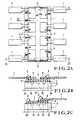
- Figs. 3A and 3Bshow a semiconductor IC device including a conventional LOC type lead frame.
- the conventional LOC type lead frameincludes leads 17 and connecting terminals 16 constituted by conductive plates and connected to the leads 17.
- An insulating film 14is formed on portions of a semiconductor pellet 11 which correspond to the connecting terminals 16.
- the LOC type lead frameis fixed on the major surface of the semiconductor pellet 11, on which active elements and the like are formed, by an adhesive agent or the like. Electrodes 15 formed on a peripheral portion of the major surface of the semiconductor pellet 11 are electrically connected to the connecting terminals 16 through bonding wires 19.
- the semiconductor IC device including the conventional LOC type lead framehas the following drawback. Since the connecting terminals 16 are arranged on the major surface of the semiconductor pellet 11, on which the active elements are formed, through the insulating film 14, the connecting terminals 16 are located close to the internal circuit formed in the semiconductor pellet 11. For this reason, if a vertical electric field is generated by the connecting terminals 16 due to voltages, such as input/output signals, externally applied to the leads 17, this electric field enters the internal circuit of the semiconductor pellet 11. Since the active elements formed on the semiconductor pellet 11 are operated by signals of low potentials, various kinds of inconvenience may be caused, e.g., the internal circuit of the semiconductor pellet 11 is influenced by the electric field, and the operation margin of the semiconductor IC device is reduced.
- a semiconductor IC devicecomprising a semiconductor pellet on which a plurality of electrodes and a plurality of active elements are formed, an insulating film bonded to a surface of the semiconductor pellet on which the active elements are formed, a conductive plate arranged on the insulating film, and a lead frame including a plurality of connecting terminals selectively arranged in predetermined regions on the conductive plate through another insulating film, and leads laterally extending from the connecting terminals.
- the conductive plateis fixed to the semiconductor pellet through the insulating film.
- the connecting terminals of the lead frameare formed on the conductive plate through another insulating film.
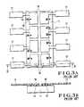
- Figs. 1A and 1Bshow a semiconductor IC device including an LOC type lead frame according to the first embodiment of the present invention.
- a conductive plate 2is bonded through a first insulating film 3 of polyimide material to a surface of a central portion 10 of a semiconductor pellet 1 on which active elements 15 including an internal circuits 15′ are formed.
- the conductive plate 2is rectangular and has a size large enough to cover the surface of the semiconductor pellet 1 except for its peripheral portion 20.
- Connecting terminals 6are bonded to predetermined regions on the conductive plate 2 through a second insulating film 4 of polyimide material.
- the conductive plate 2is made of 42 alloy metal (Ni - Fe alloy) or copper alloy as that for the lead 7, and has substantially the same planar shape as that of the pellet 1 except for the peripheral portion 20, to cover all active elements 15.
- the conductive plate 2has the same thickness as that of the lead 7.
- the respective connecting terminals 6are integrally formed with leads 7.
- the leads 7laterally extend from the semiconductor pellet 1.
- Electrodes 9are formed on the peripheral portion 20 of the semiconductor pellet 1, which is not covered with the conductive plate 2. These electrodes and the connecting terminals 6 are connected to each other through bonding wires.
- the conductive plate 2is arranged between the connecting terminals 6 and the semiconductor pellet 1, an electric field generated by the connecting terminals 6 is blocked by the conductive plate 2 and does not enter the semiconductor pellet 1. This can prevent inconvenience such as an operation error of the semiconductor IC device and a reduction in operation margin.
- Fig. 2A to 2Cshow a semiconductor IC device including an LOC type lead frame according to the second embodiment of the present invention.
- the second embodimentis different from the first embodiment in a method of connecting bonding wires. That is, the second embodiment has substantially the same structure as that of the first embodiment except for a portion associated with the above-mentioned method.
- the same reference numerals in Figs. 2A, 2B, and 2Cdenote the same parts as in Figs. 1A and 1B, and a detailed description thereof will be omitted.
- a lead frame in this embodimenthas the same structure as that of the lead frame in the first embodiment. After this lead frame is bonded to a semiconductor pellet 1, the pellet 1 is connected to connecting terminals 6 through bonding wires 5. In this embodiment, bonding is performed in the following manner.
- the connecting terminals 6are connected to electrodes such as signal lines, which are formed on the semiconductor pellet 1, through bonding wires 5.
- a predetermined connecting terminal 6 to be connected to, e.g., the power source or ground, and a conductive plate 2are connected to each other through a bonding wire 5.
- the conductive plate 2is set at the power source or ground potential.
- an electrode formed on the semiconductor pellet 1 which is to be connected to the power source or groundis connected to the conductive plate 2 through a bonding wire 5.
- the conductive plate 2is connected to the power source or ground in this manner, the power source electrode or the ground electrode formed on the semiconductor pellet 1 can be easily connected.
- the conductive plateis arranged between the connecting terminals and the semiconductor pellet. This arrangement can prevent an electric field as noise generated by the connecting terminals due to input/output signals from locally influencing the internal circuit of the semiconductor pellet.
- the conductive platecan be used as the wiring for the power source or ground potential. This greatly increases the degree of freedom in terms of the layout of a semiconductor pellet.
Landscapes
- Physics & Mathematics (AREA)
- Condensed Matter Physics & Semiconductors (AREA)
- General Physics & Mathematics (AREA)
- Engineering & Computer Science (AREA)
- Computer Hardware Design (AREA)
- Microelectronics & Electronic Packaging (AREA)
- Power Engineering (AREA)
- Lead Frames For Integrated Circuits (AREA)
- Wire Bonding (AREA)
Abstract
Description
- The present invention relates to a semiconductor IC device in which an LOC (Lead On Chip) type lead frame bonded to a semiconductor pellet is electrically connected to the semiconductor pellet through bonding wires.
- Figs. 3A and 3B show a semiconductor IC device including a conventional LOC type lead frame.
- The conventional LOC type lead frame includes
leads 17 and connectingterminals 16 constituted by conductive plates and connected to theleads 17. Aninsulating film 14 is formed on portions of asemiconductor pellet 11 which correspond to the connectingterminals 16. - The LOC type lead frame is fixed on the major surface of the
semiconductor pellet 11, on which active elements and the like are formed, by an adhesive agent or the like.Electrodes 15 formed on a peripheral portion of the major surface of thesemiconductor pellet 11 are electrically connected to the connectingterminals 16 throughbonding wires 19. - The semiconductor IC device including the conventional LOC type lead frame, however, has the following drawback. Since the connecting
terminals 16 are arranged on the major surface of thesemiconductor pellet 11, on which the active elements are formed, through theinsulating film 14, the connectingterminals 16 are located close to the internal circuit formed in thesemiconductor pellet 11. For this reason, if a vertical electric field is generated by the connectingterminals 16 due to voltages, such as input/output signals, externally applied to theleads 17, this electric field enters the internal circuit of thesemiconductor pellet 11. Since the active elements formed on thesemiconductor pellet 11 are operated by signals of low potentials, various kinds of inconvenience may be caused, e.g., the internal circuit of thesemiconductor pellet 11 is influenced by the electric field, and the operation margin of the semiconductor IC device is reduced. - It is an object of the present invention to provide a semiconductor IC device including an LOC type lead frame which can prevent an electric field from influencing a semiconductor pellet.
- In order to achieve the above object, according to the present invention, there is provided a semiconductor IC device comprising a semiconductor pellet on which a plurality of electrodes and a plurality of active elements are formed, an insulating film bonded to a surface of the semiconductor pellet on which the active elements are formed, a conductive plate arranged on the insulating film, and a lead frame including a plurality of connecting terminals selectively arranged in predetermined regions on the conductive plate through another insulating film, and leads laterally extending from the connecting terminals.
- According to the present invention, the conductive plate is fixed to the semiconductor pellet through the insulating film. The connecting terminals of the lead frame are formed on the conductive plate through another insulating film. With this arrangement, an electric field generated by the connecting terminals is blocked by the conductive plate and hence cannot enter the semiconductor pellet. Therefore, predetermined characteristics of the internal circuit of the semiconductor pellet are maintained, and inconvenience such as operation errors can be prevented.
- Fig. 1A is a plan view showing a semiconductor IC device including an LOC type lead frame according to the first embodiment of the present invention;
- Fig. 1B is a sectional view taken along a line I - I in Fig. 1A;
- Fig. 2A is a plan view showing a semiconductor IC device including an LOC type lead frame according to the second embodiment of the present invention;
- Fig. 2B is a sectional view taken along a line IIB - IIB in Fig. 2A;
- Fig. 2C is a sectional view taken along a line IIC - IIC in Fig. 2A;
- Fig. 3A is a plan view showing a conventional LOC type lead frame for a semiconductor IC device; and
- Fig. 3B is a sectional view taken along a line III - III in Fig. 3A.
- Embodiments of the present invention will be described below with reference to the accompanying drawings.
- Figs. 1A and 1B show a semiconductor IC device including an LOC type lead frame according to the first embodiment of the present invention.
- In this embodiment, a
conductive plate 2 is bonded through a firstinsulating film 3 of polyimide material to a surface of acentral portion 10 of asemiconductor pellet 1 on whichactive elements 15 including aninternal circuits 15′ are formed. Theconductive plate 2 is rectangular and has a size large enough to cover the surface of thesemiconductor pellet 1 except for itsperipheral portion 20. Connectingterminals 6 are bonded to predetermined regions on theconductive plate 2 through a secondinsulating film 4 of polyimide material. Theconductive plate 2 is made of 42 alloy metal (Ni - Fe alloy) or copper alloy as that for thelead 7, and has substantially the same planar shape as that of thepellet 1 except for theperipheral portion 20, to cover allactive elements 15. Theconductive plate 2 has the same thickness as that of thelead 7. The respective connectingterminals 6 are integrally formed withleads 7. The leads 7 laterally extend from thesemiconductor pellet 1.Electrodes 9 are formed on theperipheral portion 20 of thesemiconductor pellet 1, which is not covered with theconductive plate 2. These electrodes and the connectingterminals 6 are connected to each other through bonding wires. - In this embodiment, since the
conductive plate 2 is arranged between the connectingterminals 6 and thesemiconductor pellet 1, an electric field generated by the connectingterminals 6 is blocked by theconductive plate 2 and does not enter thesemiconductor pellet 1. This can prevent inconvenience such as an operation error of the semiconductor IC device and a reduction in operation margin. - Fig. 2A to 2C show a semiconductor IC device including an LOC type lead frame according to the second embodiment of the present invention.
- The second embodiment is different from the first embodiment in a method of connecting bonding wires. That is, the second embodiment has substantially the same structure as that of the first embodiment except for a portion associated with the above-mentioned method. The same reference numerals in Figs. 2A, 2B, and 2C denote the same parts as in Figs. 1A and 1B, and a detailed description thereof will be omitted.
- A lead frame in this embodiment has the same structure as that of the lead frame in the first embodiment. After this lead frame is bonded to a
semiconductor pellet 1, thepellet 1 is connected to connectingterminals 6 throughbonding wires 5. In this embodiment, bonding is performed in the following manner. - As shown in Fig. 2B, the connecting
terminals 6 are connected to electrodes such as signal lines, which are formed on thesemiconductor pellet 1, throughbonding wires 5. - As shown in Fig. 2C, a predetermined connecting terminal 6 to be connected to, e.g., the power source or ground, and a
conductive plate 2 are connected to each other through abonding wire 5. As a result, theconductive plate 2 is set at the power source or ground potential. - Subsequently, an electrode formed on the
semiconductor pellet 1 which is to be connected to the power source or ground is connected to theconductive plate 2 through abonding wire 5. - Since the
conductive plate 2 is connected to the power source or ground in this manner, the power source electrode or the ground electrode formed on thesemiconductor pellet 1 can be easily connected. - As has been described above, according to the present invention, the conductive plate is arranged between the connecting terminals and the semiconductor pellet. This arrangement can prevent an electric field as noise generated by the connecting terminals due to input/output signals from locally influencing the internal circuit of the semiconductor pellet. In addition, for example, the conductive plate can be used as the wiring for the power source or ground potential. This greatly increases the degree of freedom in terms of the layout of a semiconductor pellet.
Claims (5)
a semiconductor pellet on which a plurality of electrodes and a plurality of active elements are formed;
an insulating film bonded to a surface of said semiconductor pellet on which the active elements are formed;
a conductive plate arranged on said insulating film; and
a lead frame including a plurality of connecting terminals selectively arranged in predetermined regions on said conductive plate through another insulating film, and leads laterally extending from the connecting terminals.
Applications Claiming Priority (2)
| Application Number | Priority Date | Filing Date | Title |
|---|---|---|---|
| JP186600/89 | 1989-07-19 | ||
| JP1186600AJPH088330B2 (en) | 1989-07-19 | 1989-07-19 | Semiconductor integrated circuit device having LOC type lead frame |
Publications (3)
| Publication Number | Publication Date |
|---|---|
| EP0409173A2true EP0409173A2 (en) | 1991-01-23 |
| EP0409173A3 EP0409173A3 (en) | 1991-07-24 |
| EP0409173B1 EP0409173B1 (en) | 1994-10-12 |
Family
ID=16191400
Family Applications (1)
| Application Number | Title | Priority Date | Filing Date |
|---|---|---|---|
| EP90113690AExpired - LifetimeEP0409173B1 (en) | 1989-07-19 | 1990-07-17 | Semiconductor ic device having an improved interconnection structure |
Country Status (4)
| Country | Link |
|---|---|
| US (1) | US5089876A (en) |
| EP (1) | EP0409173B1 (en) |
| JP (1) | JPH088330B2 (en) |
| DE (1) | DE69013254T2 (en) |
Cited By (15)
| Publication number | Priority date | Publication date | Assignee | Title |
|---|---|---|---|---|
| EP0554742A3 (en)* | 1992-02-03 | 1993-09-08 | Motorola, Inc. | Lead-on-chip semiconductor device |
| EP0560487A3 (en)* | 1992-02-07 | 1993-12-08 | Texas Instruments Inc | Semiconductor device having a lead frame |
| EP0576708A1 (en)* | 1992-07-01 | 1994-01-05 | Siemens Aktiengesellschaft | Integrated circuit with leadframe |
| EP0503201A3 (en)* | 1990-12-20 | 1994-03-16 | Toshiba Kk | |
| EP0586163A3 (en)* | 1992-09-02 | 1994-03-23 | Texas Instruments Inc | |
| EP0594299A3 (en)* | 1992-09-18 | 1994-11-23 | Texas Instruments Inc | Multi-layered lead frame assembly and method for integrated circuits. |
| DE19835393A1 (en)* | 1998-08-05 | 1999-11-04 | Siemens Ag | Component used in high performance DRAMs |
| WO2013142112A1 (en)* | 2012-03-20 | 2013-09-26 | Allegro Microsystems, Llc | Integrated circuit package having a split lead frame |
| US9411025B2 (en) | 2013-04-26 | 2016-08-09 | Allegro Microsystems, Llc | Integrated circuit package having a split lead frame and a magnet |
| US9494660B2 (en) | 2012-03-20 | 2016-11-15 | Allegro Microsystems, Llc | Integrated circuit package having a split lead frame |
| US9620705B2 (en) | 2012-01-16 | 2017-04-11 | Allegro Microsystems, Llc | Methods and apparatus for magnetic sensor having non-conductive die paddle |
| US9812588B2 (en) | 2012-03-20 | 2017-11-07 | Allegro Microsystems, Llc | Magnetic field sensor integrated circuit with integral ferromagnetic material |
| US10234513B2 (en) | 2012-03-20 | 2019-03-19 | Allegro Microsystems, Llc | Magnetic field sensor integrated circuit with integral ferromagnetic material |
| US10921391B2 (en) | 2018-08-06 | 2021-02-16 | Allegro Microsystems, Llc | Magnetic field sensor with spacer |
| US10991644B2 (en) | 2019-08-22 | 2021-04-27 | Allegro Microsystems, Llc | Integrated circuit package having a low profile |
Families Citing this family (25)
| Publication number | Priority date | Publication date | Assignee | Title |
|---|---|---|---|---|
| US5068712A (en)* | 1988-09-20 | 1991-11-26 | Hitachi, Ltd. | Semiconductor device |
| US5432127A (en)* | 1989-06-30 | 1995-07-11 | Texas Instruments Incorporated | Method for making a balanced capacitance lead frame for integrated circuits having a power bus and dummy leads |
| US5377077A (en)* | 1990-08-01 | 1994-12-27 | Staktek Corporation | Ultra high density integrated circuit packages method and apparatus |
| EP0509065A1 (en)* | 1990-08-01 | 1992-10-21 | Staktek Corporation | Ultra high density integrated circuit packages, method and apparatus |
| US5475920A (en)* | 1990-08-01 | 1995-12-19 | Burns; Carmen D. | Method of assembling ultra high density integrated circuit packages |
| US5446620A (en)* | 1990-08-01 | 1995-08-29 | Staktek Corporation | Ultra high density integrated circuit packages |
| US5367766A (en)* | 1990-08-01 | 1994-11-29 | Staktek Corporation | Ultra high density integrated circuit packages method |
| US5227232A (en)* | 1991-01-23 | 1993-07-13 | Lim Thiam B | Conductive tape for semiconductor package, a lead frame without power buses for lead on chip package, and a semiconductor device with conductive tape power distribution |
| US5448450A (en)* | 1991-08-15 | 1995-09-05 | Staktek Corporation | Lead-on-chip integrated circuit apparatus |
| JP2634978B2 (en)* | 1991-08-29 | 1997-07-30 | 川崎製鉄株式会社 | Lead frame with protection element |
| JPH05226559A (en)* | 1991-10-11 | 1993-09-03 | Hitachi Cable Ltd | Resin-sealed semiconductor device |
| KR940006187Y1 (en)* | 1991-10-15 | 1994-09-10 | 금성일렉트론 주식회사 | Semiconductor device |
| US5311057A (en)* | 1992-11-27 | 1994-05-10 | Motorola Inc. | Lead-on-chip semiconductor device and method for making the same |
| US5302849A (en)* | 1993-03-01 | 1994-04-12 | Motorola, Inc. | Plastic and grid array semiconductor device and method for making the same |
| US5399902A (en)* | 1993-03-04 | 1995-03-21 | International Business Machines Corporation | Semiconductor chip packaging structure including a ground plane |
| US5644161A (en)* | 1993-03-29 | 1997-07-01 | Staktek Corporation | Ultra-high density warp-resistant memory module |
| US5369056A (en)* | 1993-03-29 | 1994-11-29 | Staktek Corporation | Warp-resistent ultra-thin integrated circuit package fabrication method |
| US5801437A (en)* | 1993-03-29 | 1998-09-01 | Staktek Corporation | Three-dimensional warp-resistant integrated circuit module method and apparatus |
| JP2856642B2 (en)* | 1993-07-16 | 1999-02-10 | 株式会社東芝 | Semiconductor device and manufacturing method thereof |
| US5700715A (en)* | 1994-06-14 | 1997-12-23 | Lsi Logic Corporation | Process for mounting a semiconductor device to a circuit substrate |
| US5545912A (en)* | 1994-10-27 | 1996-08-13 | Motorola, Inc. | Electronic device enclosure including a conductive cap and substrate |
| US6025642A (en)* | 1995-08-17 | 2000-02-15 | Staktek Corporation | Ultra high density integrated circuit packages |
| US5872398A (en)* | 1996-01-11 | 1999-02-16 | Micron Technology, Inc. | Reduced stress LOC assembly including cantilevered leads |
| US5945732A (en)* | 1997-03-12 | 1999-08-31 | Staktek Corporation | Apparatus and method of manufacturing a warp resistant thermally conductive integrated circuit package |
| EP2568496A3 (en) | 2011-09-09 | 2017-12-06 | Assa Abloy Ab | Method and apparatus for maintaining operational temperature of an integrated circuit |
Family Cites Families (9)
| Publication number | Priority date | Publication date | Assignee | Title |
|---|---|---|---|---|
| US3257588A (en)* | 1959-04-27 | 1966-06-21 | Rca Corp | Semiconductor device enclosures |
| US4451845A (en)* | 1981-12-22 | 1984-05-29 | Avx Corporation | Lead frame device including ceramic encapsulated capacitor and IC chip |
| US4534105A (en)* | 1983-08-10 | 1985-08-13 | Rca Corporation | Method for grounding a pellet support pad in an integrated circuit device |
| US4833521A (en)* | 1983-12-13 | 1989-05-23 | Fairchild Camera & Instrument Corp. | Means for reducing signal propagation losses in very large scale integrated circuits |
| JPS61108160A (en)* | 1984-11-01 | 1986-05-26 | Nec Corp | Semiconductor device with built-in capacitor and manufacture thereof |
| CA1238119A (en)* | 1985-04-18 | 1988-06-14 | Douglas W. Phelps, Jr. | Packaged semiconductor chip |
| US4801999A (en)* | 1987-07-15 | 1989-01-31 | Advanced Micro Devices, Inc. | Integrated circuit lead frame assembly containing voltage bussing and distribution to an integrated circuit die using tape automated bonding with two metal layers |
| EP0405871B1 (en)* | 1989-06-30 | 1999-09-08 | Texas Instruments Incorporated | Balanced capacitance lead frame for integrated circuits |
| JP6103729B2 (en) | 2015-07-15 | 2017-03-29 | サミー株式会社 | Bullet ball machine |
- 1989
- 1989-07-19JPJP1186600Apatent/JPH088330B2/ennot_activeExpired - Lifetime
- 1990
- 1990-07-17EPEP90113690Apatent/EP0409173B1/ennot_activeExpired - Lifetime
- 1990-07-17DEDE69013254Tpatent/DE69013254T2/ennot_activeExpired - Lifetime
- 1990-07-19USUS07/554,652patent/US5089876A/ennot_activeExpired - Lifetime
Cited By (30)
| Publication number | Priority date | Publication date | Assignee | Title |
|---|---|---|---|---|
| EP0503201A3 (en)* | 1990-12-20 | 1994-03-16 | Toshiba Kk | |
| US5473514A (en)* | 1990-12-20 | 1995-12-05 | Kabushiki Kaisha Toshiba | Semiconductor device having an interconnecting circuit board |
| US5613295A (en)* | 1990-12-20 | 1997-03-25 | Kabushiki Kaisha Toshiba | Semiconductor device having an interconnecting circuit board and method for manufacturing same |
| US5646830A (en)* | 1990-12-20 | 1997-07-08 | Kabushiki Kaisha Toshiba | Semiconductor device having an interconnecting circuit board |
| US5715147A (en)* | 1990-12-20 | 1998-02-03 | Kabushiki Kaisha Toshiba | Semiconductor device having an interconnecting circuit board |
| EP0843356A3 (en)* | 1992-02-03 | 1998-10-28 | Motorola, Inc. | Lead-on-chip semiconductor device |
| EP0554742A3 (en)* | 1992-02-03 | 1993-09-08 | Motorola, Inc. | Lead-on-chip semiconductor device |
| KR100276781B1 (en)* | 1992-02-03 | 2001-01-15 | 비센트 비. 인그라시아 | Lead-on-Chip Semiconductor Device and Manufacturing Method Thereof |
| EP0560487A3 (en)* | 1992-02-07 | 1993-12-08 | Texas Instruments Inc | Semiconductor device having a lead frame |
| US5804871A (en)* | 1992-02-07 | 1998-09-08 | Texas Instruments Incorporated | Lead on chip semiconductor device having bus bars and crossing leads |
| EP0576708A1 (en)* | 1992-07-01 | 1994-01-05 | Siemens Aktiengesellschaft | Integrated circuit with leadframe |
| EP0586163A3 (en)* | 1992-09-02 | 1994-03-23 | Texas Instruments Inc | |
| EP0594299A3 (en)* | 1992-09-18 | 1994-11-23 | Texas Instruments Inc | Multi-layered lead frame assembly and method for integrated circuits. |
| DE19835393A1 (en)* | 1998-08-05 | 1999-11-04 | Siemens Ag | Component used in high performance DRAMs |
| US9620705B2 (en) | 2012-01-16 | 2017-04-11 | Allegro Microsystems, Llc | Methods and apparatus for magnetic sensor having non-conductive die paddle |
| US10333055B2 (en) | 2012-01-16 | 2019-06-25 | Allegro Microsystems, Llc | Methods for magnetic sensor having non-conductive die paddle |
| WO2013142112A1 (en)* | 2012-03-20 | 2013-09-26 | Allegro Microsystems, Llc | Integrated circuit package having a split lead frame |
| US10916665B2 (en) | 2012-03-20 | 2021-02-09 | Allegro Microsystems, Llc | Magnetic field sensor integrated circuit with an integrated coil |
| US9666788B2 (en) | 2012-03-20 | 2017-05-30 | Allegro Microsystems, Llc | Integrated circuit package having a split lead frame |
| US9812588B2 (en) | 2012-03-20 | 2017-11-07 | Allegro Microsystems, Llc | Magnetic field sensor integrated circuit with integral ferromagnetic material |
| US10230006B2 (en) | 2012-03-20 | 2019-03-12 | Allegro Microsystems, Llc | Magnetic field sensor integrated circuit with an electromagnetic suppressor |
| US10234513B2 (en) | 2012-03-20 | 2019-03-19 | Allegro Microsystems, Llc | Magnetic field sensor integrated circuit with integral ferromagnetic material |
| US11961920B2 (en) | 2012-03-20 | 2024-04-16 | Allegro Microsystems, Llc | Integrated circuit package with magnet having a channel |
| US9494660B2 (en) | 2012-03-20 | 2016-11-15 | Allegro Microsystems, Llc | Integrated circuit package having a split lead frame |
| US11828819B2 (en) | 2012-03-20 | 2023-11-28 | Allegro Microsystems, Llc | Magnetic field sensor integrated circuit with integral ferromagnetic material |
| US11677032B2 (en) | 2012-03-20 | 2023-06-13 | Allegro Microsystems, Llc | Sensor integrated circuit with integrated coil and element in central region of mold material |
| US11444209B2 (en) | 2012-03-20 | 2022-09-13 | Allegro Microsystems, Llc | Magnetic field sensor integrated circuit with an integrated coil enclosed with a semiconductor die by a mold material |
| US9411025B2 (en) | 2013-04-26 | 2016-08-09 | Allegro Microsystems, Llc | Integrated circuit package having a split lead frame and a magnet |
| US10921391B2 (en) | 2018-08-06 | 2021-02-16 | Allegro Microsystems, Llc | Magnetic field sensor with spacer |
| US10991644B2 (en) | 2019-08-22 | 2021-04-27 | Allegro Microsystems, Llc | Integrated circuit package having a low profile |
Also Published As
| Publication number | Publication date |
|---|---|
| DE69013254D1 (en) | 1994-11-17 |
| US5089876A (en) | 1992-02-18 |
| JPH0350859A (en) | 1991-03-05 |
| EP0409173B1 (en) | 1994-10-12 |
| DE69013254T2 (en) | 1995-05-24 |
| EP0409173A3 (en) | 1991-07-24 |
| JPH088330B2 (en) | 1996-01-29 |
Similar Documents
| Publication | Publication Date | Title |
|---|---|---|
| EP0409173A2 (en) | Semiconductor ic device having an improved interconnection structure | |
| US6060772A (en) | Power semiconductor module with a plurality of semiconductor chips | |
| EP0142938B1 (en) | Semiconductor integrated circuit including a lead frame chip support | |
| US5528083A (en) | Thin film chip capacitor for electrical noise reduction in integrated circuits | |
| US6897569B2 (en) | Apparatus for implementing selected functionality on an integrated circuit device in an electronic device | |
| US5648679A (en) | Tape ball lead integrated circuit package | |
| JP3051011B2 (en) | Power module | |
| EP0595021A1 (en) | Improved lead frame package for electronic devices | |
| US5309021A (en) | Semiconductor device having particular power distribution interconnection arrangement | |
| JP2568748B2 (en) | Semiconductor device | |
| EP0760164B1 (en) | A high density integrated circuit assembly combining leadframe leads with conductive traces | |
| JPH04307943A (en) | Semiconductor device | |
| US5399904A (en) | Array type semiconductor device having insulating circuit board | |
| JP2987088B2 (en) | MOS technology power device chips and package assemblies | |
| JP2560805B2 (en) | Semiconductor device | |
| US5276352A (en) | Resin sealed semiconductor device having power source by-pass connecting line | |
| JP3138539B2 (en) | Semiconductor device and COB substrate | |
| EP0262493B1 (en) | Electronic package with distributed decoupling capacitors | |
| US7492038B2 (en) | Semiconductor device | |
| US20240395681A1 (en) | Semiconductor device | |
| JPH0697666A (en) | Electronic device | |
| JPH06224369A (en) | Semiconductor device | |
| JP2963548B2 (en) | Semiconductor device | |
| EP0430239A1 (en) | Resin molded semiconductor device having tab kept at desired electric potential | |
| JPH02119171A (en) | Semiconductor integrated circuit device |
Legal Events
| Date | Code | Title | Description |
|---|---|---|---|
| PUAI | Public reference made under article 153(3) epc to a published international application that has entered the european phase | Free format text:ORIGINAL CODE: 0009012 | |
| 17P | Request for examination filed | Effective date:19900717 | |
| AK | Designated contracting states | Kind code of ref document:A2 Designated state(s):DE FR GB | |
| PUAL | Search report despatched | Free format text:ORIGINAL CODE: 0009013 | |
| RHK1 | Main classification (correction) | Ipc:H01L 23/492 | |
| AK | Designated contracting states | Kind code of ref document:A3 Designated state(s):DE FR GB | |
| 17Q | First examination report despatched | Effective date:19930128 | |
| GRAA | (expected) grant | Free format text:ORIGINAL CODE: 0009210 | |
| AK | Designated contracting states | Kind code of ref document:B1 Designated state(s):DE FR GB | |
| REF | Corresponds to: | Ref document number:69013254 Country of ref document:DE Date of ref document:19941117 | |
| ET | Fr: translation filed | ||
| PLBE | No opposition filed within time limit | Free format text:ORIGINAL CODE: 0009261 | |
| STAA | Information on the status of an ep patent application or granted ep patent | Free format text:STATUS: NO OPPOSITION FILED WITHIN TIME LIMIT | |
| 26N | No opposition filed | ||
| REG | Reference to a national code | Ref country code:GB Ref legal event code:IF02 | |
| REG | Reference to a national code | Ref country code:GB Ref legal event code:732E | |
| REG | Reference to a national code | Ref country code:FR Ref legal event code:TQ | |
| REG | Reference to a national code | Ref country code:GB Ref legal event code:732E | |
| REG | Reference to a national code | Ref country code:FR Ref legal event code:TP | |
| PGFP | Annual fee paid to national office [announced via postgrant information from national office to epo] | Ref country code:FR Payment date:20090710 Year of fee payment:20 | |
| PGFP | Annual fee paid to national office [announced via postgrant information from national office to epo] | Ref country code:GB Payment date:20090715 Year of fee payment:20 Ref country code:DE Payment date:20090709 Year of fee payment:20 | |
| REG | Reference to a national code | Ref country code:GB Ref legal event code:PE20 Expiry date:20100716 | |
| PG25 | Lapsed in a contracting state [announced via postgrant information from national office to epo] | Ref country code:GB Free format text:LAPSE BECAUSE OF EXPIRATION OF PROTECTION Effective date:20100716 | |
| PG25 | Lapsed in a contracting state [announced via postgrant information from national office to epo] | Ref country code:DE Free format text:LAPSE BECAUSE OF EXPIRATION OF PROTECTION Effective date:20100717 |