EP0402759B1 - Portable electronic device having versatile program storage - Google Patents
Portable electronic device having versatile program storageDownload PDFInfo
- Publication number
- EP0402759B1 EP0402759B1EP90110739AEP90110739AEP0402759B1EP 0402759 B1EP0402759 B1EP 0402759B1EP 90110739 AEP90110739 AEP 90110739AEP 90110739 AEP90110739 AEP 90110739AEP 0402759 B1EP0402759 B1EP 0402759B1
- Authority
- EP
- European Patent Office
- Prior art keywords
- card
- data
- program
- memory means
- line mode
- Prior art date
- Legal status (The legal status is an assumption and is not a legal conclusion. Google has not performed a legal analysis and makes no representation as to the accuracy of the status listed.)
- Expired - Lifetime
Links
Images


Classifications
- G—PHYSICS
- G07—CHECKING-DEVICES
- G07F—COIN-FREED OR LIKE APPARATUS
- G07F7/00—Mechanisms actuated by objects other than coins to free or to actuate vending, hiring, coin or paper currency dispensing or refunding apparatus
- G07F7/08—Mechanisms actuated by objects other than coins to free or to actuate vending, hiring, coin or paper currency dispensing or refunding apparatus by coded identity card or credit card or other personal identification means
- G07F7/10—Mechanisms actuated by objects other than coins to free or to actuate vending, hiring, coin or paper currency dispensing or refunding apparatus by coded identity card or credit card or other personal identification means together with a coded signal, e.g. in the form of personal identification information, like personal identification number [PIN] or biometric data
- G07F7/1008—Active credit-cards provided with means to personalise their use, e.g. with PIN-introduction/comparison system
- G—PHYSICS
- G06—COMPUTING OR CALCULATING; COUNTING
- G06Q—INFORMATION AND COMMUNICATION TECHNOLOGY [ICT] SPECIALLY ADAPTED FOR ADMINISTRATIVE, COMMERCIAL, FINANCIAL, MANAGERIAL OR SUPERVISORY PURPOSES; SYSTEMS OR METHODS SPECIALLY ADAPTED FOR ADMINISTRATIVE, COMMERCIAL, FINANCIAL, MANAGERIAL OR SUPERVISORY PURPOSES, NOT OTHERWISE PROVIDED FOR
- G06Q20/00—Payment architectures, schemes or protocols
- G06Q20/30—Payment architectures, schemes or protocols characterised by the use of specific devices or networks
- G06Q20/34—Payment architectures, schemes or protocols characterised by the use of specific devices or networks using cards, e.g. integrated circuit [IC] cards or magnetic cards
- G06Q20/341—Active cards, i.e. cards including their own processing means, e.g. including an IC or chip
- G06Q20/3415—Cards acting autonomously as pay-media
- G—PHYSICS
- G06—COMPUTING OR CALCULATING; COUNTING
- G06Q—INFORMATION AND COMMUNICATION TECHNOLOGY [ICT] SPECIALLY ADAPTED FOR ADMINISTRATIVE, COMMERCIAL, FINANCIAL, MANAGERIAL OR SUPERVISORY PURPOSES; SYSTEMS OR METHODS SPECIALLY ADAPTED FOR ADMINISTRATIVE, COMMERCIAL, FINANCIAL, MANAGERIAL OR SUPERVISORY PURPOSES, NOT OTHERWISE PROVIDED FOR
- G06Q20/00—Payment architectures, schemes or protocols
- G06Q20/30—Payment architectures, schemes or protocols characterised by the use of specific devices or networks
- G06Q20/34—Payment architectures, schemes or protocols characterised by the use of specific devices or networks using cards, e.g. integrated circuit [IC] cards or magnetic cards
- G06Q20/357—Cards having a plurality of specified features
- G06Q20/3576—Multiple memory zones on card
Definitions
- the present inventionrelates to a multifunctional portable electronic device such as an IC card, which incorporates, e.g., a CPU, a data memory, a built-in battery, and the like, and is solely used to provide an electronic calculator function, a time display function, and the like, and is inserted in a terminal in use.
- a multifunctional portable electronic devicesuch as an IC card, which incorporates, e.g., a CPU, a data memory, a built-in battery, and the like, and is solely used to provide an electronic calculator function, a time display function, and the like, and is inserted in a terminal in use.
- An IC card of this typeincorporates a CPU (control element), a data memory, and the like as well as a keyboard, a display unit, and the like, and is solely used to provide an electronic calculator function, a time display function, or the like, or is inserted in a terminal in use.
- the CPU, the data memory, and the likeare incorporated as an LSI.
- a programis examined according to specifications presented by a customer, and thereafter, programming, debugging, tests, and the like are performed. Then, the manufacture of a new LSI is started from design of a mask. In this case, basic functions are stored in a program memory comprising a mask ROM.
- DE-A-38 11 831discloses a portable electronic device according to the preamble of claim 1.
- the known portable electronic devicecan be used in connection with an external apparatus (on-line mode) or without an external apparatus (off-line mode).
- FR-A-2 591 008discloses a portable electronic device, which is cooperating with an external terminal and, thus, is operable in an on-line mode.
- the systemcomprises an EEPROM and an EPROM. Data input from the external device are stored either in the EEPROM or in the EPROM depending on additional data added to the data to be stored.
- a portable electronic device of the present inventioncomprises the features mentioned in claim 1. Access to the second memory means is enabled in the on-line mode but is disabled in the off-line mode.
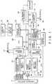
- Figs. 1 to 5are views for explaining an embodiment of the present invention, in which:
- reference numeral 10denotes an IC card as a portable electronic device, which is a multifunctional IC card having various functions (applications).
- IC card 10has an on-line function (on-line mode) used with a terminal (not shown), an off-line function (off-line mode) in which IC card 10 is solely operated, and a standby state wherein only a timepiece function is enabled.
- the off-line functionincludes an electronic calculator mode in which the card can be used as an electronic calculator, a clock mode for displaying a time of a timepiece for a user, an electronic note (memorandum) mode in which addresses, names, telephone numbers, and the like are registered or read out, and a purchase mode in which IC card 10 is utilized as a plurality of kinds of credit cards.
- IC card 10can be solely used in the mode of this function.
- IC card 10stores a balance, a valid date, purchase records, and the like. Upon every purchase, a purchase amount is subtracted from the balance stored in IC card 10 and purchase information is recorded. When the balance in IC card 10 becomes zero or the valid date expires, a secret code is issued from a contract bank, thus updating the contents of the IC card.
- Contacts portion 11includes a plurality of terminals 11a to 11f, i.e., an operation power supply voltage (Vcc, +5 V) terminal, an EEPROM write power supply voltage terminal (Vpp, +12 V to +24 V), a ground terminal, a clock signal terminal, a reset signal terminal, and data I/O terminals.
- Vccoperation power supply voltage
- VppEEPROM write power supply voltage terminal
- selection keysM1, M2, M3, and M4
- 12afor selecting processing operations corresponding to kinds of card, i.e., various credit cards, cash cards, and the like
- ten-key pad 12bi.e., ten-key pad 12b
- Addition key 12cis used as a NEXT key, i.e., a mode selection key for selecting a mode during a display of a date and time in the off-line mode.
- Subtraction key 12dis used as a BACK key, i.e., a key for returning a display state of display unit 13 to a previous state.
- Multiplication key 12fis used as a start key.
- Decimal point key 12gis used as a NO key or an end key.
- Equal key 12his used as a YES key or a power-on key.
- a CPU(to be described later) is released from a HALT state, and causes display unit 13 to display time and date as an operation start message.
- Addition key 12c as the mode selection keyis used as a key for advancing the display state of display unit 13 which is displaying date and time to another mode. Every time addition key 12c is depressed, the electronic memorandum, time set, date set, purchase transaction modes, and the like are displayed on display unit 13 as a menu. When these modes are executed, equal key 12h is depressed as the YES key. Thus, the selected mode can be executed.
- Display unit 13is a 16-digit display, each digit of which has a 5 ⁇ 7 dot matrix.
- Fig. 3shows an outer appearance of IC card reader/writer 16 connected to a terminal dealing with IC card 10 (e.g., a personal computer). More specifically, reader/writer 16 is electrically connected to contacts portion 11 of IC card 10 inserted from card slot 17, and reads or writes data from or in a memory of IC card 10.
- IC card reader/writer 16is electrically connected to contacts portion 11 of IC card 10 inserted from card slot 17, and reads or writes data from or in a memory of IC card 10.
- IC card reader/writer 16is connected to a main body of personal computer PC through a cable.
- An electrical circuit of IC card 10is arranged, as shown in Fig. 1.
- This circuitadopts a low-power consumption design using the CMOS techniques.
- the electrical circuitcomprises contacts portion 11, communication circuit 21, reset circuit 22, power supply regulator 23, internal battery (built-in battery) 25 of, e.g., 3 V, battery checker 24 for checking if a voltage value of built-in battery 25 is equal to or higher than a rated value, clock controller 26, oscillator 27, as an arithmetic clock quartz oscillator, for outputting a signal at an oscillation frequency of 200 kHz (high-speed clock), control CPU (central processing unit) 28, mask ROM 29 for storing a basic program and data necessary for it, work memory 30, data memory 31, comprising an EEPROM, for storing an ID number, data, and the like, and a user program and the basic program, memory controller 40 for controlling mask ROM 29 and data memory 31, timer 32 used for measuring time during a processing operation, calender circuit 33, oscillator 34, as a fundamental clock quartz
- Communication circuit 21, CPU 28, ROM 29, memory controller 40, work memory 30, data memory 31, timer 32, calender circuit 33, display controller 35, and keyboard interface 38are connected to each other through data bus 20.
- communication circuit 21converts serial I/O signals supplied from IC card reader/writer 16 through contacts portion 11 into parallel data, and outputs it onto data bus 20.
- circuit 21converts parallel data supplied from data bus 20 into serial I/O signals, and outputs them to IC card reader/writer 16 through contacts portion 11. In this case, the format content of conversion is determined by the terminal and IC card 10.
- Reset circuit 22generates a reset signal to start CPU 28 when the on-line mode is set.
- Power supply regulator 23switches a drive mode from one by built-in battery 25 to the other by an external power supply after the lapse of a predetermined period of time from the beginning of the on-line mode.
- regulator 23switches the drive mode from one by the external power supply to the other by built-in battery 25.
- Clock controller 26appropriately switches the low- and high-speed clocks in the off-line mode in which a card operation is performed by built-in battery 25. For the purpose of power saving, after execution of a HALT command, controller 26 stops oscillator 27 which outputs a signal of an oscillation frequency of 200 kHz (high-speed clock), thereby stopping supply of a clock to CPU 28. Then, controller 26 waits in a perfect HALT state. Clock controller 26 basically selects a time-piece clock upon execution of the HALT command.
- the basic program stored in mask ROM 29includes a credit function, a drive program for I/O control, a calender function, and various other subroutine functions.
- Data memory 31consists of memory area 31a for storing a user application program, memory area 31b for storing user data, and memory area 31c for basic program data, which serves as a preservation data area for storing the basic program, as shown in Fig. 4.
- the basic program stored in mask ROM 29is loaded before the manufacture of an LSI.
- the user application program stored in data memory 31is loaded from the terminal as part of card issuance processing at an issuer upon completion of the manufacture of a card.
- Memory controller 40monitors operations of mask ROM 29 and data memory 31 and controls data read/write access so as to prevent basic data from being destroyed by bugs in software or noise or an illegal program from entering a user area (to prevent the basic program from being illegally modified).
- the basic programis illegally modified, if card 10 is, for example, a cash card, the balance of the bank account of the card is not decreased although a user makes a purchase using this card.
- memory controller 40In the on-line mode in which external power supply voltage Vcc is supplied, memory controller 40 enables data read/write access to user data memory area 31b. In the off-line mode in which external power supply voltage Vcc is not supplied, controller 40 disables data read/write access to user data memory area 31b.
- Calender circuit 33has a timepiece which can be desirably set and updated by a card holder, and a transaction timepiece in which a world standard time is set upon issuance of the card and cannot be changed.
- Display controller 35converts display data supplied from CPU 28 into a character pattern using a character generator (not shown) comprising an internal ROM, and displays the character pattern on display unit 13 using display driver 36.
- Keyboard interface 38converts an input operation at keyboard 12 into a corresponding key input signal, and outputs it to CPU 28.
- Memory controller 40is arranged, as shown in Fig. 5. More specifically, controller 40 includes user area address memory 51 for storing several upper bits of a start address of user application program memory area 31a as data e51 indicating memory area 31a of data memory 31. Data e51 from user area address memory 51 is output to address comparator 52.
- Address comparator 52compares data e51 supplied from user area address memory 51 and several upper bits (upper 4 bits of 8-bit data) of access address e20 supplied from CPU 28 through data bus 20. When a coincidence between the two addresses is detected, comparator 52 outputs a "1" signal as coincidence signal e52; otherwise, it outputs a "0" signal as a noncoincidence signal.
- the signal from address comparator 52is supplied to one input terminal of NAND gate 53.
- the other input terminal of NAND gate 53receives external power supply voltage Vcc from contacts portion 11 through inverter 54.
- the output from NAND gate 53is supplied to select terminal S of data selector 55.
- Chip select terminal of data selector 55receives a read signal from CPU 28 through data bus 20, and data input terminal A receives read data from data memory 31, which is stored in read buffer 56.
- Data input terminal B of selector 55receives a software interruption instruction code stored in software interruption instruction code register 57.
- Output Y of data selector 55is output to CPU 28 through data bus 20.
- the read signal supplied from CPU 28 through data bus 20is directly output to data memory 31.
- Read buffer 56stores read data supplied from data memory 31.
- Software interruption instruction code register 57stores a software interruption vector address "00" (start address of a software interruption instruction of mask ROM 29) for causing a software interruption to CPU 28.
- the software interruption instructionis part of the basic program, and is a program for invalidating (resetting) the presently executed program. This instruction is stored in mask ROM 29.
- a write signal supplied from CPU 28 through data bus 20is supplied to chip select terminal CS of write buffer 58, and is also supplied to one input terminal of NAND gate 60 through inverter 59.
- Write data supplied from CPU 28 through data bus 20is supplied to the data input terminal of write buffer 58.
- the other input terminal of NAND gate 60receives a signal from NAND gate 53, and the output from NAND gate 60 is output to data memory 31 as a write signal.
- a read address and a read signalare supplied from CPU 28 to memory controller 40 through data bus 20 in a read mode. More specifically, the read address is supplied to address comparator 52, and is also output to data memory 31. The read signal is supplied to chip select terminal CS of data selector 55, and is also output to data memory 31.
- Address comparator 52compares the read address with data from user area address memory 51. If comparator 52 determines that the read address falls within user application program memory area 31a, it outputs a "1" signal to NAND gate 53; otherwise, it outputs a "0" signal to NAND gate 53.
- NAND gate 53when the read address is present in memory area 31a and no external power supply voltage Vcc is supplied (in the off-line mode), NAND gate 53 outputs a "0" signal as a read disable signal. When the read address falls outside memory area 31a or when the read address falls within memory area 31a and external power supply voltage Vcc is supplied (in the on-line mode), NAND gate 53 outputs a "1" signal as a read enable signal.
- data selector 55selects read data from data memory 31, which is stored in read buffer 56, and outputs it to CPU 28 through data bus 20. Upon reception of the read data, CPU 28 ends read processing.
- data selector 55selects the software interruption instruction code "00" stored in software interruption instruction code register 57, and outputs it to CPU 28 through data bus 20.
- CPU 28Upon reception of the software interruption instruction code "00", CPU 28 reads out a software interruption instruction program from mask ROM 29, and executes processing according to the readout program, i.e., processing for resetting the presently executed program.
- CPU 28supplies a write address, a write signal, and write data to memory controller 40 through data bus 20.
- the write addressis supplied to address comparator 52, and is also output to data memory 31.
- the write signalis supplied to chip select terminal CS of write buffer 58, and is also output to NAND gate 60 through inverter 59.
- Address comparator 52compares the input write address and data supplied from user area address memory 51. When the comparison result indicates that the write address falls within user application program memory area 31a, comparator 52 outputs a "1" signal to NAND gate 53; otherwise, it outputs a "0" signal to NAND gate 53.
- NAND gate 60When the output from NAND gate 53 is the "1" signal, NAND gate 60 is kept enabled; when it is the "0" signal, NAND gate 60 is disabled.
- a user programis loaded in the rewritable data memory.
- the read modewhen a read address corresponds to the user program in data memory 31 and no external power supply voltage is supplied, i.e., in the off-line mode, data read access to the data memory is disabled.
- the external power supply voltageis supplied, i.e., in the on-line mode, data read access to the data memory is enabled.
- the write modewhen a write address corresponds to the user program and no external power supply voltage is supplied, i.e., in the off-line mode, data write access to the data memory is disabled.
- the external power supply voltageis supplied, i.e., in the on-line mode, data write access to the data memory is enabled.
- an IC cardis used.
- the present inventionis not limited to this.
- the present inventioncan be applied to various other portable electronic devices as long as they have a data memory and a control element, and can selectively perform I/Os from an external device.
- the electronic deviceneed not always have a card-like shape but may have other shapes such as a rod-like shape.
- the battery shown in Fig. 1may be a solar cell.
- a portable electronic devicewhich can prevent an increase in cost and can shorten a development period can be provided.
Landscapes
- Engineering & Computer Science (AREA)
- Business, Economics & Management (AREA)
- General Physics & Mathematics (AREA)
- Physics & Mathematics (AREA)
- Accounting & Taxation (AREA)
- Computer Networks & Wireless Communication (AREA)
- Microelectronics & Electronic Packaging (AREA)
- Strategic Management (AREA)
- General Business, Economics & Management (AREA)
- Theoretical Computer Science (AREA)
- Storage Device Security (AREA)
- Credit Cards Or The Like (AREA)
- Calculators And Similar Devices (AREA)
- Stored Programmes (AREA)
Description
- The present invention relates to a multifunctional portable electronic device such as an IC card, which incorporates, e.g., a CPU, a data memory, a built-in battery, and the like, and is solely used to provide an electronic calculator function, a time display function, and the like, and is inserted in a terminal in use.
- Conventionally, multifunctional IC cards have been developed. An IC card of this type incorporates a CPU (control element), a data memory, and the like as well as a keyboard, a display unit, and the like, and is solely used to provide an electronic calculator function, a time display function, or the like, or is inserted in a terminal in use. The CPU, the data memory, and the like are incorporated as an LSI.
- In an IC card of this type, a program is examined according to specifications presented by a customer, and thereafter, programming, debugging, tests, and the like are performed. Then, the manufacture of a new LSI is started from design of a mask. In this case, basic functions are stored in a program memory comprising a mask ROM.
- For this reason, every time specifications are changed or a new function is added, an LSI must be manufactured, resulting in high cost of the LSI, i.e., an IC card. In addition, a development period (mainly for a program) is undesirably prolonged.
- DE-A-38 11 831 discloses a portable electronic device according to the preamble of
claim 1. The known portable electronic device can be used in connection with an external apparatus (on-line mode) or without an external apparatus (off-line mode). - FR-A-2 591 008 discloses a portable electronic device, which is cooperating with an external terminal and, thus, is operable in an on-line mode. The system comprises an EEPROM and an EPROM. Data input from the external device are stored either in the EEPROM or in the EPROM depending on additional data added to the data to be stored.
- It is an object of the present invention to provide a portable electronic device which can prevent an increase in cost, and can shorten a development period.
- A portable electronic device of the present invention comprises the features mentioned in
claim 1. Access to the second memory means is enabled in the on-line mode but is disabled in the off-line mode. - This invention can be more fully understood from the following detailed description when taken in conjunction with the accompanying drawings, in which:
- Figs. 1 to 5 are views for explaining an embodiment of the present invention, in which:
- Fig. 1 is a schematic block diagram showing an arrangement of an electrical circuit of an IC card;
- Fig. 2 is a plan view showing an arrangement of the IC card;
- Fig. 3 is a perspective view showing a terminal for the IC card;
- Fig. 4 shows a memory map of a data memory; and
- Fig. 5 is a circuit diagram showing an arrangement of a memory controller.
- An embodiment of the present invention will be described below with reference to the accompanying drawings.
- In Fig. 2,
reference numeral 10 denotes an IC card as a portable electronic device, which is a multifunctional IC card having various functions (applications). For example,IC card 10 has an on-line function (on-line mode) used with a terminal (not shown), an off-line function (off-line mode) in whichIC card 10 is solely operated, and a standby state wherein only a timepiece function is enabled. - The off-line function includes an electronic calculator mode in which the card can be used as an electronic calculator, a clock mode for displaying a time of a timepiece for a user, an electronic note (memorandum) mode in which addresses, names, telephone numbers, and the like are registered or read out, and a purchase mode in which
IC card 10 is utilized as a plurality of kinds of credit cards. Thus,IC card 10 can be solely used in the mode of this function. - In the purchase mode,
IC card 10 stores a balance, a valid date, purchase records, and the like. Upon every purchase, a purchase amount is subtracted from the balance stored inIC card 10 and purchase information is recorded. When the balance inIC card 10 becomes zero or the valid date expires, a secret code is issued from a contract bank, thus updating the contents of the IC card. Contacts portion 11 arranged at a position designated by the standards of a card,keyboard 12 including 20 keys, anddisplay unit 13 arranged on a surface portion abovekeyboard 12 and formed of a liquid crystal element are arranged on the surface ofIC card 10.Contacts portion 11 includes a plurality of terminals 11a to 11f, i.e., an operation power supply voltage (Vcc, +5 V) terminal, an EEPROM write power supply voltage terminal (Vpp, +12 V to +24 V), a ground terminal, a clock signal terminal, a reset signal terminal, and data I/O terminals.Keyboard 12 includes selection keys (M1, M2, M3, and M4) 12a for selecting processing operations corresponding to kinds of card, i.e., various credit cards, cash cards, and the like, ten-key pad 12b, four-arithmetic rule keys, that is, addition (+) key 12c, subtraction (-)key 12d, division (÷)key 12e, multiplication (×)key 12f, decimal point (.) key 12g, and equal (=)key 12h.- Addition key 12c is used as a NEXT key, i.e., a mode selection key for selecting a mode during a display of a date and time in the off-line mode.
Subtraction key 12d is used as a BACK key, i.e., a key for returning a display state ofdisplay unit 13 to a previous state.Multiplication key 12f is used as a start key. Decimal point key 12g is used as a NO key or an end key.Equal key 12h is used as a YES key or a power-on key. - When
equal key 12h is depressed as the power-on key, a CPU (to be described later) is released from a HALT state, and causesdisplay unit 13 to display time and date as an operation start message. - In this state, when keys of ten-
key pad 12b are depressed,IC card 10 is set in the electronic calculator mode, and four arithmetic operations can be performed. - Addition key 12c as the mode selection key is used as a key for advancing the display state of
display unit 13 which is displaying date and time to another mode. Every time addition key 12c is depressed, the electronic memorandum, time set, date set, purchase transaction modes, and the like are displayed ondisplay unit 13 as a menu. When these modes are executed,equal key 12h is depressed as the YES key. Thus, the selected mode can be executed. Display unit 13 is a 16-digit display, each digit of which has a 5 × 7 dot matrix.- Fig. 3 shows an outer appearance of IC card reader/
writer 16 connected to a terminal dealing with IC card 10 (e.g., a personal computer). More specifically, reader/writer 16 is electrically connected tocontacts portion 11 ofIC card 10 inserted fromcard slot 17, and reads or writes data from or in a memory ofIC card 10. - IC card reader/
writer 16 is connected to a main body of personal computer PC through a cable. - An electrical circuit of
IC card 10 is arranged, as shown in Fig. 1. This circuit adopts a low-power consumption design using the CMOS techniques. The electrical circuit comprisescontacts portion 11,communication circuit 21,reset circuit 22,power supply regulator 23, internal battery (built-in battery) 25 of, e.g., 3 V,battery checker 24 for checking if a voltage value of built-inbattery 25 is equal to or higher than a rated value,clock controller 26,oscillator 27, as an arithmetic clock quartz oscillator, for outputting a signal at an oscillation frequency of 200 kHz (high-speed clock), control CPU (central processing unit) 28,mask ROM 29 for storing a basic program and data necessary for it,work memory 30,data memory 31, comprising an EEPROM, for storing an ID number, data, and the like, and a user program and the basic program,memory controller 40 for controllingmask ROM 29 anddata memory 31,timer 32 used for measuring time during a processing operation,calender circuit 33,oscillator 34, as a fundamental clock quartz oscillator, for outputting a signal at an oscillation frequency of 32.768 kHz (low-speed clock),display controller 35,display driver 36 fordriving display unit 13, andkeyboard interface 38 as a key input circuit forkeyboard 12. Communication circuit 21,CPU 28,ROM 29,memory controller 40,work memory 30,data memory 31,timer 32,calender circuit 33,display controller 35, andkeyboard interface 38 are connected to each other throughdata bus 20.- In a reception mode,
communication circuit 21 converts serial I/O signals supplied from IC card reader/writer 16 throughcontacts portion 11 into parallel data, and outputs it ontodata bus 20. In a transmission mode,circuit 21 converts parallel data supplied fromdata bus 20 into serial I/O signals, and outputs them to IC card reader/writer 16 throughcontacts portion 11. In this case, the format content of conversion is determined by the terminal andIC card 10. Reset circuit 22 generates a reset signal to startCPU 28 when the on-line mode is set.Power supply regulator 23 switches a drive mode from one by built-inbattery 25 to the other by an external power supply after the lapse of a predetermined period of time from the beginning of the on-line mode. When the off-line mode is set, i.e., an external voltage is decreased,regulator 23 switches the drive mode from one by the external power supply to the other by built-inbattery 25.Clock controller 26 appropriately switches the low- and high-speed clocks in the off-line mode in which a card operation is performed by built-inbattery 25. For the purpose of power saving, after execution of a HALT command,controller 26 stopsoscillator 27 which outputs a signal of an oscillation frequency of 200 kHz (high-speed clock), thereby stopping supply of a clock toCPU 28. Then,controller 26 waits in a perfect HALT state.Clock controller 26 basically selects a time-piece clock upon execution of the HALT command.- The basic program stored in
mask ROM 29 includes a credit function, a drive program for I/O control, a calender function, and various other subroutine functions. Data memory 31 consists ofmemory area 31a for storing a user application program,memory area 31b for storing user data, and memory area 31c for basic program data, which serves as a preservation data area for storing the basic program, as shown in Fig. 4.- The basic program stored in
mask ROM 29 is loaded before the manufacture of an LSI. The user application program stored indata memory 31 is loaded from the terminal as part of card issuance processing at an issuer upon completion of the manufacture of a card. Memory controller 40 monitors operations ofmask ROM 29 anddata memory 31 and controls data read/write access so as to prevent basic data from being destroyed by bugs in software or noise or an illegal program from entering a user area (to prevent the basic program from being illegally modified). When the basic program is illegally modified, ifcard 10 is, for example, a cash card, the balance of the bank account of the card is not decreased although a user makes a purchase using this card.- In the on-line mode in which external power supply voltage Vcc is supplied,
memory controller 40 enables data read/write access to userdata memory area 31b. In the off-line mode in which external power supply voltage Vcc is not supplied,controller 40 disables data read/write access to userdata memory area 31b. Calender circuit 33 has a timepiece which can be desirably set and updated by a card holder, and a transaction timepiece in which a world standard time is set upon issuance of the card and cannot be changed.Display controller 35 converts display data supplied fromCPU 28 into a character pattern using a character generator (not shown) comprising an internal ROM, and displays the character pattern ondisplay unit 13 usingdisplay driver 36.Keyboard interface 38 converts an input operation atkeyboard 12 into a corresponding key input signal, and outputs it toCPU 28.Memory controller 40 is arranged, as shown in Fig. 5. More specifically,controller 40 includes userarea address memory 51 for storing several upper bits of a start address of user applicationprogram memory area 31a as data e51 indicatingmemory area 31a ofdata memory 31. Data e51 from userarea address memory 51 is output to addresscomparator 52.Address comparator 52 compares data e51 supplied from userarea address memory 51 and several upper bits (upper 4 bits of 8-bit data) of access address e20 supplied fromCPU 28 throughdata bus 20. When a coincidence between the two addresses is detected,comparator 52 outputs a "1" signal as coincidence signal e52; otherwise, it outputs a "0" signal as a noncoincidence signal.- The signal from
address comparator 52 is supplied to one input terminal ofNAND gate 53. The other input terminal ofNAND gate 53 receives external power supply voltage Vcc fromcontacts portion 11 throughinverter 54. - The output from
NAND gate 53 is supplied to select terminal S ofdata selector 55. Chip select terminal ofdata selector 55 receives a read signal fromCPU 28 throughdata bus 20, and data input terminal A receives read data fromdata memory 31, which is stored in readbuffer 56. Data input terminal B ofselector 55 receives a software interruption instruction code stored in software interruptioninstruction code register 57. - Output Y of
data selector 55 is output toCPU 28 throughdata bus 20. The read signal supplied fromCPU 28 throughdata bus 20 is directly output todata memory 31. Readbuffer 56 stores read data supplied fromdata memory 31. - Software interruption
instruction code register 57 stores a software interruption vector address "00" (start address of a software interruption instruction of mask ROM 29) for causing a software interruption toCPU 28. The software interruption instruction is part of the basic program, and is a program for invalidating (resetting) the presently executed program. This instruction is stored inmask ROM 29. - A write signal supplied from
CPU 28 throughdata bus 20 is supplied to chip select terminal CS ofwrite buffer 58, and is also supplied to one input terminal ofNAND gate 60 throughinverter 59. Write data supplied fromCPU 28 throughdata bus 20 is supplied to the data input terminal ofwrite buffer 58. The other input terminal ofNAND gate 60 receives a signal fromNAND gate 53, and the output fromNAND gate 60 is output todata memory 31 as a write signal. - The operation of the above arrangement will be described below. Assume that a read address and a read signal are supplied from
CPU 28 tomemory controller 40 throughdata bus 20 in a read mode. More specifically, the read address is supplied to addresscomparator 52, and is also output todata memory 31. The read signal is supplied to chip select terminal CS ofdata selector 55, and is also output todata memory 31. Address comparator 52 compares the read address with data from userarea address memory 51. Ifcomparator 52 determines that the read address falls within user applicationprogram memory area 31a, it outputs a "1" signal toNAND gate 53; otherwise, it outputs a "0" signal toNAND gate 53.- When external power supply voltage Vcc is supplied from IC card reader/
writer 16 tomemory controller 40 throughcontacts portion 11, a "0" signal is supplied toNAND gate 53 throughinverter 54. When no external power supply voltage Vcc is supplied from IC card reader/writer 16 tomemory controller 40 throughcontacts portion 11, a "1" signal is supplied toNAND gate 53 throughinverter 54. - Therefore, when the read address is present in
memory area 31a and no external power supply voltage Vcc is supplied (in the off-line mode),NAND gate 53 outputs a "0" signal as a read disable signal. When the read address falls outsidememory area 31a or when the read address falls withinmemory area 31a and external power supply voltage Vcc is supplied (in the on-line mode),NAND gate 53 outputs a "1" signal as a read enable signal. - Thus, when the output from
NAND gate 53 is the "1" signal,data selector 55 selects input terminal A; when it is the "0" signal,selector 55 selects input terminal B. - Data at an address of
data memory 31 designated by the input read signal and the input read address is read out, and is output to readbuffer 56. Thus, read data is stored in readbuffer 56. - As a result, when input terminal A is selected,
data selector 55 selects read data fromdata memory 31, which is stored in readbuffer 56, and outputs it toCPU 28 throughdata bus 20. Upon reception of the read data,CPU 28 ends read processing. - When input terminal B is selected,
data selector 55 selects the software interruption instruction code "00" stored in software interruptioninstruction code register 57, and outputs it toCPU 28 throughdata bus 20. - Upon reception of the software interruption instruction code "00",
CPU 28 reads out a software interruption instruction program frommask ROM 29, and executes processing according to the readout program, i.e., processing for resetting the presently executed program. - In a write mode,
CPU 28 supplies a write address, a write signal, and write data tomemory controller 40 throughdata bus 20. The write address is supplied to addresscomparator 52, and is also output todata memory 31. The write signal is supplied to chip select terminal CS ofwrite buffer 58, and is also output toNAND gate 60 throughinverter 59. Address comparator 52 compares the input write address and data supplied from userarea address memory 51. When the comparison result indicates that the write address falls within user applicationprogram memory area 31a,comparator 52 outputs a "1" signal toNAND gate 53; otherwise, it outputs a "0" signal toNAND gate 53.- When external power supply voltage Vcc is supplied from IC card reader/
writer 16 tomemory controller 40 throughcontacts portion 11, a "0" signal is supplied toNAND gate 53 throughinverter 54. When no external power supply voltage Vcc is supplied from IC card reader/writer 16 tomemory controller 40 throughcontacts portion 11, a "1" signal is supplied toNAND gate 53 throughinverter 54. - Therefore, when the write address falls within
memory area 31a (output fromcomparator 52 = "1") and no external power supply voltage Vcc is supplied (in the off-line mode; output frominverter 54 = "1"),NAND gate 53 outputs a "0" signal as a write disable signal. Otherwise, that is, when the write address falls outsidememory area 31a (output fromcomparator 52 = "0") or when the write address falls withinmemory area 31a and external power supply voltage Vcc is supplied (in the on-line mode; output frominverter 54 = "0"),NAND gate 53 outputs a "1" signal as a write enable signal. - When the output from
NAND gate 53 is the "1" signal,NAND gate 60 is kept enabled; when it is the "0" signal,NAND gate 60 is disabled. - As a result, when
NAND gate 60 is enabled and the write signal fromCPU 28 is supplied todata memory 31,data memory 31 stores write data supplied fromwrite buffer 58 at the input write address. WhenNAND gate 60 is kept disabled and no write signal fromCPU 28 is output,data memory 31 does not perform a storage operation of write data. - As described above, a user program is loaded in the rewritable data memory. In the read mode, when a read address corresponds to the user program in
data memory 31 and no external power supply voltage is supplied, i.e., in the off-line mode, data read access to the data memory is disabled. When the external power supply voltage is supplied, i.e., in the on-line mode, data read access to the data memory is enabled. In the write mode, when a write address corresponds to the user program and no external power supply voltage is supplied, i.e., in the off-line mode, data write access to the data memory is disabled. When the external power supply voltage is supplied, i.e., in the on-line mode, data write access to the data memory is enabled. - Thus, there can be provided a highly reliable card which can prevent basic data from being destroyed and illegal software from entering by monitoring a user program operation without preparing a new LSI every time specifications are modified.
- In the above embodiment, when an external power supply voltage Vcc is supplied, i.e., in the on-line mode, read/write access of the user program is enabled. However, the present invention is not limited to this. For example, when an internal power supply voltage is supplied, i.e., in the off-line mode, read/write access of the user program may be enabled.
- In the above embodiment, an IC card is used. However, the present invention is not limited to this. The present invention can be applied to various other portable electronic devices as long as they have a data memory and a control element, and can selectively perform I/Os from an external device. The electronic device need not always have a card-like shape but may have other shapes such as a rod-like shape. The battery shown in Fig. 1 may be a solar cell.
- As described above, according to the present invention, a portable electronic device which can prevent an increase in cost and can shorten a development period can be provided.
Claims (10)
- A portable electronic device, which has an on-line mode in which the device in use is connected to an external apparatus and has an off-line mode in which the device is solely used, comprising:
a data processing unit (28) having a function of basic processing for the device and a function of user application processing;
nonrewritable first memory means (31c) for storing a program for executing the basic processing; and
rewritable second memory means (31a, 31b) for storing a program for executing a user application processing;
characterized by control means (40) for permitting said data processing unit to enable read/write access to the second memory means in the on-line mode, and to disable read/write access to said second memory means in the off-line mode,
said control means (40) including:
comparison means (51, 52) for comparing a start address of the user application processing program, stored in said second memory means, and an address output from said data processing unit, and for, when a coincidence between the two addresses is detected, outputting a coincidence signal; and
circuit means (53, 54, 59, 60) for, when the coincidence signal is output and said IC card is powered by a built-in battery (25), disabling said data processing unit from accessing said second memory means, and for, when the coincidence signal is not output or said IC card is powered by said external apparatus, enabling said data processing unit to access said second memory means. - A device according to claim 1, characterized in that said second memory means includes an electrically-erasable programmable ROM.
- A device according to claim 2, characterized in that said electrically-erasable programmable ROM stores the program for the user application processing and a user's identification number.
- A device according to claim 1, 2 or 3 characterized in that said first memory means includes a ROM.
- A device according to claim 4, characterized in that said ROM stores the program for executing the basic processing and data used when the program is executed.
- A device of any of claims 1 to 5, incorporated in an IC card.
- A device according to claim 6, characterized in that the function of said basic processing includes a credit transaction function.
- A device according to claim 6, characterized in that the function of said basic processing includes a calendar function.
- A device according to claim 8, further comprising:
a calendar circuit (33) including a user timepiece which can be desirably set by a user, and a timepiece which can be set by an issuer of said IC card but cannot be optionally set by the user. - A device of any of claims 1 to 9, characterized in that it is incorporated in an IC card powered by said external apparatus in the on-line mode, and is powered by said built-in battery in the off-line mode.
Applications Claiming Priority (2)
| Application Number | Priority Date | Filing Date | Title |
|---|---|---|---|
| JP148994/89 | 1989-06-12 | ||
| JP1148994AJPH0314083A (en) | 1989-06-12 | 1989-06-12 | portable electronic devices |
Publications (3)
| Publication Number | Publication Date |
|---|---|
| EP0402759A2 EP0402759A2 (en) | 1990-12-19 |
| EP0402759A3 EP0402759A3 (en) | 1991-07-31 |
| EP0402759B1true EP0402759B1 (en) | 1994-10-12 |
Family
ID=15465329
Family Applications (1)
| Application Number | Title | Priority Date | Filing Date |
|---|---|---|---|
| EP90110739AExpired - LifetimeEP0402759B1 (en) | 1989-06-12 | 1990-06-06 | Portable electronic device having versatile program storage |
Country Status (4)
| Country | Link |
|---|---|
| US (1) | US5168151A (en) |
| EP (1) | EP0402759B1 (en) |
| JP (1) | JPH0314083A (en) |
| DE (1) | DE69013233T2 (en) |
Cited By (1)
| Publication number | Priority date | Publication date | Assignee | Title |
|---|---|---|---|---|
| US10187904B2 (en) | 2008-02-29 | 2019-01-22 | Koninklijke Kpn N.V. | Telecommunications network and method for time-based network access |
Families Citing this family (53)
| Publication number | Priority date | Publication date | Assignee | Title |
|---|---|---|---|---|
| DK174975B1 (en)* | 1988-05-06 | 2004-04-05 | Toppan Printing Co Ltd | Integrated circuit board |
| US6926200B1 (en)* | 1989-09-06 | 2005-08-09 | Fujitsu Limited | Electronic cashless system |
| JP3016490B2 (en)* | 1990-09-28 | 2000-03-06 | 富士写真フイルム株式会社 | IC memory card |
| US5579528A (en)* | 1991-12-31 | 1996-11-26 | Dell Usa, L.P. | Computer system employing docking bay with spring loaded connector pins and file coherency method |
| JPH05274282A (en)* | 1992-03-30 | 1993-10-22 | Canon Inc | Method for information processing and device therefor |
| JP3058986B2 (en)* | 1992-04-02 | 2000-07-04 | ダイヤセミコンシステムズ株式会社 | Computer system power saving controller |
| JP2842750B2 (en)* | 1992-04-07 | 1999-01-06 | 三菱電機株式会社 | IC card |
| DE4220809A1 (en)* | 1992-06-25 | 1994-01-05 | Benno Stoerkle | Payment system |
| DE69324445T2 (en)* | 1992-11-27 | 1999-09-30 | Denso Corp., Kariya | Portable electronic device |
| ATE161348T1 (en)* | 1992-12-01 | 1998-01-15 | Landis & Gyr Tech Innovat | PROCEDURE FOR COMPENSATION FOR SERVICES AND/OR GOODS AND FACILITY FOR IMPLEMENTING THE PROCESS |
| US5737610A (en)* | 1993-02-16 | 1998-04-07 | Infopak Inc. | System and method for providing data and program code to a card for use by a reader |
| US5477215A (en)* | 1993-08-02 | 1995-12-19 | At&T Corp. | Arrangement for simultaneously interrogating a plurality of portable radio frequency communication devices |
| US5590038A (en)* | 1994-06-20 | 1996-12-31 | Pitroda; Satyan G. | Universal electronic transaction card including receipt storage and system and methods of conducting electronic transactions |
| US6925439B1 (en) | 1994-06-20 | 2005-08-02 | C-Sam, Inc. | Device, system and methods of conducting paperless transactions |
| US5754762A (en)* | 1997-01-13 | 1998-05-19 | Kuo; Chih-Cheng | Secure multiple application IC card using interrupt instruction issued by operating system or application program to control operation flag that determines the operational mode of bi-modal CPU |
| US6073856A (en)* | 1997-09-05 | 2000-06-13 | Dai Nippon Printing Co., Ltd. | Noncontact IC device |
| US20040167823A1 (en)* | 1997-09-08 | 2004-08-26 | Neely Robert Alan | Automated electronic payment system |
| US6044362A (en)* | 1997-09-08 | 2000-03-28 | Neely; R. Alan | Electronic invoicing and payment system |
| JPH1185724A (en)* | 1997-09-12 | 1999-03-30 | Oki Electric Ind Co Ltd | Cpu mode switch circuit |
| SE520101C2 (en) | 1998-05-13 | 2003-05-27 | Axis Ab | Integrated circuit and method to induce an integrated circuit to execute instructions |
| US6651149B1 (en)* | 1998-12-10 | 2003-11-18 | Kabushiki Kaisha Toshiba | Data storage medium with certification data |
| US7308426B1 (en) | 1999-08-11 | 2007-12-11 | C-Sam, Inc. | System and methods for servicing electronic transactions |
| JP3750494B2 (en)* | 1999-08-31 | 2006-03-01 | 松下電器産業株式会社 | Semiconductor device |
| WO2001029762A2 (en)* | 1999-10-20 | 2001-04-26 | Spyrus, Inc. | Method and system for an integrated circuit card interface device with multiple modes of operation |
| US6705520B1 (en) | 1999-11-15 | 2004-03-16 | Satyan G. Pitroda | Point of sale adapter for electronic transaction device |
| EP1113387A3 (en)* | 1999-12-31 | 2001-11-21 | SCHLUMBERGER Systèmes | Smart card having a non-volatile memory with a novel mapping |
| CA2396266C (en) | 2000-01-12 | 2007-03-13 | Metavante Corporation | Integrated systems for electronic bill presentment and payment |
| US7848972B1 (en) | 2000-04-06 | 2010-12-07 | Metavante Corporation | Electronic bill presentment and payment systems and processes |
| EP1168259A3 (en)* | 2000-06-28 | 2003-12-17 | Hitachi, Ltd. | Data management method and system for IC card |
| US7529563B1 (en) | 2000-07-10 | 2009-05-05 | Pitroda Satyan G | System for distribution and use of virtual stored value cards |
| WO2002011019A1 (en) | 2000-08-01 | 2002-02-07 | First Usa Bank, N.A. | System and method for transponder-enabled account transactions |
| US7206768B1 (en) | 2000-08-14 | 2007-04-17 | Jpmorgan Chase Bank, N.A. | Electronic multiparty accounts receivable and accounts payable system |
| JP2002109169A (en) | 2000-09-29 | 2002-04-12 | Hitachi Ltd | Work support method, system, and recording medium recording work support method |
| US6631849B2 (en) | 2000-12-06 | 2003-10-14 | Bank One, Delaware, National Association | Selectable multi-purpose card |
| US7702579B2 (en)* | 2000-12-19 | 2010-04-20 | Emergis Technologies, Inc. | Interactive invoicer interface |
| US20070198432A1 (en) | 2001-01-19 | 2007-08-23 | Pitroda Satyan G | Transactional services |
| US7526449B1 (en) | 2001-04-17 | 2009-04-28 | Jpmorgan Chase Bank N.A. | Optically encoded card and system and method for using |
| JP3641230B2 (en)* | 2001-10-22 | 2005-04-20 | 株式会社東芝 | Apparatus and method for controlling a memory card |
| US8392301B1 (en) | 2002-03-08 | 2013-03-05 | Jpmorgan Chase Bank, N.A. | Financial system for isolated economic environment |
| US7593875B2 (en) | 2002-03-08 | 2009-09-22 | Jp Morgan Chase Bank | Financial system for isolated economic environment |
| US20040210498A1 (en)* | 2002-03-29 | 2004-10-21 | Bank One, National Association | Method and system for performing purchase and other transactions using tokens with multiple chips |
| JP4349788B2 (en)* | 2002-10-31 | 2009-10-21 | パナソニック株式会社 | Semiconductor integrated circuit device |
| US20040153359A1 (en)* | 2003-01-31 | 2004-08-05 | Mein-Kai Ho | Integrated supply chain management |
| US7591419B2 (en)* | 2006-03-28 | 2009-09-22 | HSBC Card Services Inc. | User selectable functionality facilitator |
| USD582977S1 (en) | 2008-02-21 | 2008-12-16 | Jpmorgan Chase Bank, N.A. | Transaction device |
| USD582476S1 (en) | 2008-02-21 | 2008-12-09 | Jpmorgan Chase Bank, N.A. | Pivoting transaction device |
| USD576671S1 (en) | 2008-02-21 | 2008-09-09 | Jpmorganchase Bank, N.A. | Overlapping transaction device |
| USD635186S1 (en) | 2008-06-30 | 2011-03-29 | Jpmorgan Chase Bank, N.A. | Metal transaction device |
| US9305292B1 (en) | 2008-07-03 | 2016-04-05 | Jpmorgan Chase Bank, N.A. | Systems and methods for providing an adaptable transponder device |
| USD636021S1 (en) | 2008-07-17 | 2011-04-12 | Jpmorgan Chase Bank, N.A. | Eco-friendly transaction device |
| US20100191652A1 (en)* | 2009-01-23 | 2010-07-29 | Eckert Daniel J | Systems and methods for adding functionality to a uis for use at a point of interaction |
| USD602986S1 (en) | 2009-03-06 | 2009-10-27 | Jpmorgan Chase Bank, N.A. | Metal transaction device |
| EP3396656A1 (en)* | 2017-04-28 | 2018-10-31 | Biegert & Funk Product GmbH & Co. KG | Display device for displaying a selection of predetermined display elements |
Family Cites Families (26)
| Publication number | Priority date | Publication date | Assignee | Title |
|---|---|---|---|---|
| FR2455320B1 (en)* | 1979-04-25 | 1986-01-24 | Cii Honeywell Bull | DEVICE FOR RECYCLING IDENTIFIABLE RECORDING MEDIA USING IDENTIFICATION DATA AND NON-VOLATILE DELETE MONOLITHIC MEMORY COMPOUNDS |
| DE3318101A1 (en)* | 1983-05-18 | 1984-11-22 | Siemens AG, 1000 Berlin und 8000 München | CIRCUIT ARRANGEMENT WITH A STORAGE AND ACCESS CONTROL UNIT |
| JPS6019277A (en)* | 1983-07-12 | 1985-01-31 | Toshiba Corp | card system |
| JPS6048555A (en)* | 1983-08-25 | 1985-03-16 | Fujitsu Kiden Ltd | Security system of magnetic card read-write device |
| US4754418A (en)* | 1984-03-27 | 1988-06-28 | Casio Computer Co., Ltd. | Combined electronic calculator and credit card |
| EP0167044B1 (en)* | 1984-06-19 | 1992-03-04 | Casio Computer Company Limited | Intelligent card |
| JPS61264485A (en)* | 1985-05-18 | 1986-11-22 | Hitachi Maxell Ltd | Reader and writer for integrated circuit card |
| JPS6250983A (en)* | 1985-08-30 | 1987-03-05 | Toshiba Corp | Memory card with display function |
| EP0218176B1 (en)* | 1985-10-07 | 1991-11-13 | Kabushiki Kaisha Toshiba | Portable electronic device |
| FR2591008B1 (en)* | 1985-11-30 | 1991-05-17 | Toshiba Kk | PORTABLE ELECTRONIC DEVICE |
| JPS62162183A (en)* | 1986-01-13 | 1987-07-18 | Toshiba Corp | Ic card |
| JPS62237592A (en)* | 1986-04-08 | 1987-10-17 | Casio Comput Co Ltd | Clock switching method in IC card |
| US4816654A (en)* | 1986-05-16 | 1989-03-28 | American Telephone And Telegraph Company | Improved security system for a portable data carrier |
| US4816653A (en)* | 1986-05-16 | 1989-03-28 | American Telephone And Telegraph Company | Security file system for a portable data carrier |
| GB2191029B (en)* | 1986-05-29 | 1990-12-12 | Almex Systems Ltd | Electronic pass |
| US4804825A (en)* | 1986-06-17 | 1989-02-14 | Casio Computer Co., Ltd. | I C card system |
| DE3628253A1 (en)* | 1986-08-20 | 1988-02-25 | Bosch Gmbh Robert | Dispensing system for goods or services which has electronic storage and control devices operable by means of value cards (chip cards) |
| JP2597553B2 (en)* | 1986-08-29 | 1997-04-09 | 株式会社東芝 | IC card |
| US4777355A (en)* | 1986-12-24 | 1988-10-11 | Mitsubishi Denki Kabushiki Kaisha | IC card and system for checking the functionality thereof |
| FR2611954B1 (en)* | 1987-03-02 | 1992-02-14 | Crouzet Sa | UNIVERSAL BASE FOR ELECTRONIC PAYMENT TERMINAL |
| US4814591A (en)* | 1987-04-13 | 1989-03-21 | Kabushiki Kaisha Toshiba | Portable medium |
| JPS63262783A (en)* | 1987-04-20 | 1988-10-31 | Toshiba Corp | portable media |
| JP2635601B2 (en)* | 1987-07-28 | 1997-07-30 | 株式会社東芝 | Portable electronic devices |
| JP2554676B2 (en)* | 1987-11-12 | 1996-11-13 | 株式会社東芝 | Portable electronic devices |
| US4983816A (en)* | 1988-02-24 | 1991-01-08 | Kabushiki Kaisha Toshiba | Portable electronic device |
| JPH01263893A (en)* | 1988-04-15 | 1989-10-20 | Toshiba Corp | Portable electronic device |
- 1989
- 1989-06-12JPJP1148994Apatent/JPH0314083A/enactivePending
- 1990
- 1990-06-06USUS07/533,880patent/US5168151A/ennot_activeExpired - Fee Related
- 1990-06-06DEDE69013233Tpatent/DE69013233T2/ennot_activeExpired - Fee Related
- 1990-06-06EPEP90110739Apatent/EP0402759B1/ennot_activeExpired - Lifetime
Cited By (1)
| Publication number | Priority date | Publication date | Assignee | Title |
|---|---|---|---|---|
| US10187904B2 (en) | 2008-02-29 | 2019-01-22 | Koninklijke Kpn N.V. | Telecommunications network and method for time-based network access |
Also Published As
| Publication number | Publication date |
|---|---|
| EP0402759A3 (en) | 1991-07-31 |
| DE69013233T2 (en) | 1995-05-24 |
| JPH0314083A (en) | 1991-01-22 |
| US5168151A (en) | 1992-12-01 |
| DE69013233D1 (en) | 1994-11-17 |
| EP0402759A2 (en) | 1990-12-19 |
Similar Documents
| Publication | Publication Date | Title |
|---|---|---|
| EP0402759B1 (en) | Portable electronic device having versatile program storage | |
| US4814591A (en) | Portable medium | |
| US5072103A (en) | Electrically powered portable medium | |
| US4766294A (en) | Portable medium | |
| US4973828A (en) | Portable electronic medium | |
| US4924075A (en) | Smart IC card | |
| US4719338A (en) | Pocket calculator with credit card controller and dispenser | |
| EP0401806B1 (en) | Portable electronic device having improved power source | |
| EP0402758B1 (en) | Portable electronic device having versatile program storage | |
| EP0306821B1 (en) | Electronic device with calendar function | |
| JP2597553B2 (en) | IC card | |
| JP2554676B2 (en) | Portable electronic devices | |
| JP2692905B2 (en) | Portable electronic devices | |
| JPS63262783A (en) | portable media | |
| JPH0236492A (en) | Portable electronic device | |
| JPH036718A (en) | Portable medium | |
| JPH0314052A (en) | portable media | |
| JPS6320680A (en) | Ic card device | |
| JPH0746294B2 (en) | Portable electronic device | |
| JPS6358520A (en) | portable media | |
| JPS6362086A (en) | Portable medium | |
| JPH01207890A (en) | Portable electronic device | |
| JPS6358547A (en) | Portable medium | |
| JPH01126790A (en) | Portable medium | |
| JPS63203396A (en) | IC card with built-in power supply |
Legal Events
| Date | Code | Title | Description |
|---|---|---|---|
| PUAI | Public reference made under article 153(3) epc to a published international application that has entered the european phase | Free format text:ORIGINAL CODE: 0009012 | |
| 17P | Request for examination filed | Effective date:19900606 | |
| AK | Designated contracting states | Kind code of ref document:A2 Designated state(s):DE FR | |
| PUAL | Search report despatched | Free format text:ORIGINAL CODE: 0009013 | |
| AK | Designated contracting states | Kind code of ref document:A3 Designated state(s):DE FR | |
| 17Q | First examination report despatched | Effective date:19930507 | |
| GRAA | (expected) grant | Free format text:ORIGINAL CODE: 0009210 | |
| AK | Designated contracting states | Kind code of ref document:B1 Designated state(s):DE FR | |
| REF | Corresponds to: | Ref document number:69013233 Country of ref document:DE Date of ref document:19941117 | |
| ET | Fr: translation filed | ||
| PLBE | No opposition filed within time limit | Free format text:ORIGINAL CODE: 0009261 | |
| STAA | Information on the status of an ep patent application or granted ep patent | Free format text:STATUS: NO OPPOSITION FILED WITHIN TIME LIMIT | |
| 26N | No opposition filed | ||
| PGFP | Annual fee paid to national office [announced via postgrant information from national office to epo] | Ref country code:DE Payment date:19990607 Year of fee payment:10 | |
| PGFP | Annual fee paid to national office [announced via postgrant information from national office to epo] | Ref country code:FR Payment date:19990610 Year of fee payment:10 | |
| PG25 | Lapsed in a contracting state [announced via postgrant information from national office to epo] | Ref country code:FR Free format text:LAPSE BECAUSE OF NON-PAYMENT OF DUE FEES Effective date:20010228 | |
| REG | Reference to a national code | Ref country code:FR Ref legal event code:ST | |
| PG25 | Lapsed in a contracting state [announced via postgrant information from national office to epo] | Ref country code:DE Free format text:LAPSE BECAUSE OF NON-PAYMENT OF DUE FEES Effective date:20010403 |