EP0369773A2 - Queue buffer memory control system - Google Patents
Queue buffer memory control systemDownload PDFInfo
- Publication number
- EP0369773A2 EP0369773A2EP89311832AEP89311832AEP0369773A2EP 0369773 A2EP0369773 A2EP 0369773A2EP 89311832 AEP89311832 AEP 89311832AEP 89311832 AEP89311832 AEP 89311832AEP 0369773 A2EP0369773 A2EP 0369773A2
- Authority
- EP
- European Patent Office
- Prior art keywords
- queue buffer
- data
- buffer memory
- request signal
- signal
- Prior art date
- Legal status (The legal status is an assumption and is not a legal conclusion. Google has not performed a legal analysis and makes no representation as to the accuracy of the status listed.)
- Granted
Links
Images


Classifications
- G—PHYSICS
- G06—COMPUTING OR CALCULATING; COUNTING
- G06F—ELECTRIC DIGITAL DATA PROCESSING
- G06F5/00—Methods or arrangements for data conversion without changing the order or content of the data handled
- G06F5/06—Methods or arrangements for data conversion without changing the order or content of the data handled for changing the speed of data flow, i.e. speed regularising or timing, e.g. delay lines, FIFO buffers; over- or underrun control therefor
- G06F5/16—Multiplexed systems, i.e. using two or more similar devices which are alternately accessed for enqueue and dequeue operations, e.g. ping-pong buffers
- G—PHYSICS
- G06—COMPUTING OR CALCULATING; COUNTING
- G06F—ELECTRIC DIGITAL DATA PROCESSING
- G06F13/00—Interconnection of, or transfer of information or other signals between, memories, input/output devices or central processing units
- G06F13/14—Handling requests for interconnection or transfer
- G06F13/16—Handling requests for interconnection or transfer for access to memory bus
- G06F13/18—Handling requests for interconnection or transfer for access to memory bus based on priority control
- G—PHYSICS
- G06—COMPUTING OR CALCULATING; COUNTING
- G06F—ELECTRIC DIGITAL DATA PROCESSING
- G06F5/00—Methods or arrangements for data conversion without changing the order or content of the data handled
- G06F5/06—Methods or arrangements for data conversion without changing the order or content of the data handled for changing the speed of data flow, i.e. speed regularising or timing, e.g. delay lines, FIFO buffers; over- or underrun control therefor
Definitions
- the present inventionrelates to a queue buffer memory control system, more particularly, it relates to management of a busy state (busy management) of the queue buffer memory provided between a main storage unit and an external storage unit in a data processing system.
- a queue buffer memoryis usually provided between the main storage unit and the external storage unit.
- the multiprocessor systemwhich is constituted by a plurality of clusters, each having central processing units, main storage units and channel processors.
- the queue buffer memoryhas a buffer function to solve an unbalanced state in which the read/write speed of the external storage unit is slower than that of the main storage unit so that these units operate asynchronously with each other.
- a queue buffer memory control systemfor managing the busy state of data at a queue buffer memory provided between a main storage unit and an external storage unit, including: a control unit for receiving a request signal from a central processing unit, selecting priority order of the request signal and decoding a destination command included in the request signal as to whether or not the request signal indicates an access to said queue buffer memory; an output data detection unit operatively connected to the queue buffer memory for detecting data quantity output from the queue buffer memory and outputting a detection signal at every detection of the data; an input data detection unit operatively connected to an output side of the control unit for detecting existence of data to be transferred to the queue buffer memory based on the destination command of the request signal, and outputting a detection signal when the input data detection unit detects the request signal before the main storage unit receives the request signal; and a data read/write indication unit operatively connected the input data detection unit and the output data detection unit for detecting the data quantity to be transferred to the queue buffer memory based on the difference between the detection
- Fig. 1is a schematic block diagram of a queue buffer memory control system of an existing type.
- reference number 1denotes a priority selection circuit
- 2a main memory
- 3a divider
- 4a queue buffer
- 5a busy state management circuit
- 6a queue buffer output control circuit
- 7an external memory.
- 21 to 26denote registers
- 34 to 50 and 53denote signal lines.
- the busy state management circuit 5for controlling the data transfer between the main memory and the queue buffer.
- the busy state management circuit 5has the function of detecting the data quantity just stored in the queue buffer 4 based on the difference between the data quantity input from the main memory 2 to the queue buffer 4 and the data quantity output from the queue buffer 4 to the external memory 7. Further, the busy management circuit 5 has the function of outputting a busy signal for stopping a write request for writing the data into the queue buffer 4 when the data quantity at the queue buffer 4 reaches a predetermined limit of the capacity of the queue buffer memory. In this case, the limit of the capacity is determined by taking account of the data existing on the line between the main memory 2 and the queue buffer 4.
- ⁇clock pulse period
- the busy state management circuit 5outputs the busy signal at the timing when the data quantity reaches 12 data blocks (32 minus 20) as the predetermined limit of the capacity at the queue buffer 4. That is, the busy signal must be output at that timing by taking into account data existing on the line.
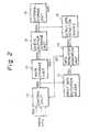
- FIG. 2is a basic block diagram of a queue buffer memory control system embodying the present invention.
- reference number 10denotes a control unit, 11 a main storage unit, 12 a queue buffer memory, 13 a input data detection unit, 14 a data read/stop indication unit, 15 an output data detection unit, and 16 an external storage unit.
- the control unit 10receives a request signal REQ from a central processing unit CPU and selects a priority order.
- the queue buffer memory 12stores the data DATA read out from the main storage unit 11 which outputs the data after receiving a request signal REQ from the control unit 10.
- the output data detection unit 15outputs a detection signal DS2 for each data input from the queue buffer memory 12.
- the input data detection unit 13detects the request signal REQ before this signal REQ is input to the main storage unit 11 and outputs a detection signal DS1 indicating the data to be input to the main storage unit 11 at every detection of the request signal REQ.
- the detection signals DS1 and DS2are input to the data read/stop indication unit 14.
- the data read/stop indication unit 14detects the data quantity to be stored in the queue buffer memory 12.
- the data read/stop indication unit 14outputs a stop signal ST to the control unit 10 to stop the request signal REQ when the data quantity reaches the maximum quantity possible to store in the queue buffer memory 12. Accordingly, using the present invention, the data to be input to the queue buffer memory 12 can be detected in the previous stage read out from the main storage unit 11. Therefore, it is not necessary to take into account the data existing on the line between the main storage unit 11 and the queue buffer memory 12 and it is possible to effectively utilize the capacity of the queue buffer memory until reading a maximum state.
- Figure 3is a schematic block diagram of a queue buffer memory control system according to an embodiment of the present invention.
- reference number 1denotes a priority selection circuit
- 2a main memory
- 3a dividing circuit
- 4a queue buffer
- 5a busy management circuit
- 6a queue buffer output control circuit
- 21 to 26 registersand 31 to 50 and 53 signal lines.
- queue buffer 4can store thirty two blocks of data as the maximum capacity.
- the request signals REQ from the CPU'sare transferred to the corresponding registers 21 to 23 through the signal lines 31 to 33.
- the priority selection circuit 1selects the priority order of the request signal REQ output from each register through the signal lines 34 to 36.
- the priority selection circuit 1outputs an access signal AC to the main memory 2 after determination of the priority order of the request signal REQ.
- the data stored in the main memory 2is read out therefrom based on the access signal AC and transferred to the dividing circuit 3.
- the datais distributed to a corresponding register 24 to 26 in accordance with the kind of request, i.e., read request, write request and the like as shown in detail in Fig. 4. This is because the request signal includes a destination command indicating the destination of the data transfer.
- the datais written into the queue buffer 4 through the register 24 and the signal line 43. Further, this data is also written into the external storage unit 7 through the signal line 48 under the predetermined conditions of the external storage unit 7.
- the queue buffer output control circuit 6outputs an output enable signal OE to the queue buffer 4 through the signal line 53 and the data stored in the queue buffer 4 is output to the external storage unit 7 through the signal line 48 if a busy signal BS is not output from the external storage unit 7 through the signal line 49.
- the queue buffer output control circuit 6outputs an information signal IS1 to the busy management circuit 5 to inform the fact that the data is output from the queue buffer 4 to the external storage unit 7.
- the information signal IS1is output from the queue buffer output control circuit 6 every time the above operation is carried out.
- the priority selection circuit 1decodes each request signal REQ input from each register 21 to 23, and detects whether or not information indicating the data transfer from the main memory to the queue buffer 4 is included in the request signal REQ based on the destination command included therein. Further, the priority selection circuit 1 outputs an information signal IS2 to the busy management circuit 5. The information signal IS2 is output from the priority selection circuit 1 to the busy management circuit 5 at every detection of the destination command.
- the information signals IS1 and IS2are input to the busy management circuit 5.
- the formeris output from the queue buffer output control circuit 6 and the latter is output from the priority selection circuit 1.
- the busy management circuit 5can detect the data quantity stored in the queue buffer 4 based on the difference between the information signals IS1 and IS2. Therefore, the busy management circuit 5 can output the busy signal BS to the priority selection circuit 1 when the data quantity reaches thirty two blocks of data in the queue buffer 4 based on the above calculation.
- the priority selection circuit 1receives the busy signal BS, the priority selection circuit 1 temporarily stops the request signal REQ to prevent writing data into the queue buffer 4 as shown in detail in Fig. 4.
- FIG. 4is a detailed circuit diagram of the circuit shown in Fig. 3.
- the priority selection circuit 1comprises a priority selector 11, a pipe-line unit 12 and a decoder 13.
- the queue buffer 4is preferably divided into two blocks 41 and 42 for discriminating whether the area in question is associated with a read operation or a write operation.
- the queue buffer output control circuit 6 in Fig. 3is included in the block 42.
- the busy state management circuit 5is mainly constituted by a counter 51 and a comparator 52.
- the decoder 13decodes the destination command included in each request signal REQ as to whether or not the destination command indicates the request of the data to be written into the external memory 7 through the main memory 2 and the queue buffer 42.
- the decoder 13outputs the information signal IS2 to the counter 51 when the decoder 13 decodes such a request signal.
- the information signal IS1is output from the queue buffer output control circuit 6 and input to the counter 51 to count it down.
- the comparator 52compares the information signal IS2 with the information signal IS2 based on the count value. Further, the comparator outputs a busy signal BS to the priority selector 11 when the count value exceeds the predetermined limit of the capacity of the queue buffer memory 4.
- the pipe-line 12is provided as a shift register for delaying the request signal. This delay is performed to coincide the transfer speed of the request signal with the read-out speed of the data from the main memory 2. Accordingly, the input timing of the request signal to the divider 3 is coincided with that of the read-out data to the divider 3.
- the divider 3is provided for dividing the request signal in accordance with the destination command included in each request signal as explained above. When the request indicates an access of the queue buffer 42, the data is transferred from the main memory 2 to the queue buffer 42 through the signal line 4. Other destinations 1 to 3 are returned to, for example, the CPU.
- the external storage unit (SSU) 7is provided for cluster management in the multiprocessor system.
- One external storage unitis connected in parallel to a plurality of clusters.
- the structure of the multiprocessor systemis omitted to simplify the explanation of the present invention.
Landscapes
- Engineering & Computer Science (AREA)
- Theoretical Computer Science (AREA)
- Physics & Mathematics (AREA)
- General Engineering & Computer Science (AREA)
- General Physics & Mathematics (AREA)
- Memory System Of A Hierarchy Structure (AREA)
- Information Transfer Systems (AREA)
- Multi Processors (AREA)
- Memory System (AREA)
Abstract
Description
- The present invention relates to a queue buffer memory control system, more particularly, it relates to management of a busy state (busy management) of the queue buffer memory provided between a main storage unit and an external storage unit in a data processing system.
- In a data processing system constituted by central processing units (CPU), main storage units (MSU), channel processors, and an external storage unit (SSU), a queue buffer memory is usually provided between the main storage unit and the external storage unit. In this case, only one external storage unit is provided in the multiprocessor system which is constituted by a plurality of clusters, each having central processing units, main storage units and channel processors.
- When data is read out from the main storage unit and the data is also written into the external storage unit, the data is temporarily stored in the queue buffer memory and the data stored in the queue buffer memory is also written into the external storage unit. Accordingly, the queue buffer memory has a buffer function to solve an unbalanced state in which the read/write speed of the external storage unit is slower than that of the main storage unit so that these units operate asynchronously with each other.
- In this case, there is a limit to the capacity of the queue buffer memory. Accordingly, it is necessary to effectively manage the busy state of queue buffer memory so that it is possible to raise the data transfer speed between the main storage unit and the external storage unit.
- It is therefore desirable to provide queue buffer memory control system enabling effective management of the busy state of the queue buffer memory.
- In accordance with the present invention, there is provided a queue buffer memory control system for managing the busy state of data at a queue buffer memory provided between a main storage unit and an external storage unit, including: a control unit for receiving a request signal from a central processing unit, selecting priority order of the request signal and decoding a destination command included in the request signal as to whether or not the request signal indicates an access to said queue buffer memory; an output data detection unit operatively connected to the queue buffer memory for detecting data quantity output from the queue buffer memory and outputting a detection signal at every detection of the data; an input data detection unit operatively connected to an output side of the control unit for detecting existence of data to be transferred to the queue buffer memory based on the destination command of the request signal, and outputting a detection signal when the input data detection unit detects the request signal before the main storage unit receives the request signal; and a data read/write indication unit operatively connected the input data detection unit and the output data detection unit for detecting the data quantity to be transferred to the queue buffer memory based on the difference between the detection signals, and generating a stop signal to send to the control unit for stopping input of the request signal having the destination command of the data transfer from the main memory unit to the queue buffer memory when the data quantity at the queue buffer memory has reached a predetermined maximum quantity.
- Reference is made, by way of example, to the accompanying drawings in which:-
- Fig. 1 is a schematic block of a queue buffer memory control system of an existing type;
- Fig. 2 is a basic block diagram of queue buffer memory control system according to the present invention;
- Fig. 3 is a schematic block diagram of a queue buffer memory control system according to an embodiment of the present invention; and
- Fig. 4 is a detailed circuit diagram of the queue buffer memory control system shown in Fig. 3.
- Before describing the preferred embodiments, an explanation will be given of problems of the present technology.
- Fig. 1 is a schematic block diagram of a queue buffer memory control system of an existing type.
- In Fig. 1,
reference number 1 denotes a priority selection circuit, 2 a main memory, 3 a divider, 4 a queue buffer, 5 a busy state management circuit, 6 a queue buffer output control circuit, and 7 an external memory. Further, 21 to 26 denote registers, and 34 to 50 and 53 denote signal lines. - For example, when data is sequentially read out from the
main memory 2 and written into thequeue buffer 4, the data quantity exceeds the capacity of thequeue buffer 4 if a write enabling signal is not generated from theexternal memory 7 to thequeue buffer 4 and thequeue buffer memory 4 cannot transfer the data to the external storage unit. Accordingly, it is necessary to provide the busystate management circuit 5 for controlling the data transfer between the main memory and the queue buffer. - The busy
state management circuit 5 has the function of detecting the data quantity just stored in thequeue buffer 4 based on the difference between the data quantity input from themain memory 2 to thequeue buffer 4 and the data quantity output from thequeue buffer 4 to theexternal memory 7. Further, thebusy management circuit 5 has the function of outputting a busy signal for stopping a write request for writing the data into thequeue buffer 4 when the data quantity at thequeue buffer 4 reaches a predetermined limit of the capacity of the queue buffer memory. In this case, the limit of the capacity is determined by taking account of the data existing on the line between themain memory 2 and thequeue buffer 4. - In general, several τ (τ: clock pulse period) are necessary as the transfer time from the reading out of the data at the
main memory 2 until the writing of that data at thequeue buffer 4. Assuming that thequeue buffer 4 can store thirty-two blocks of data as the maximum capacity and that the transfer time is 20 τ, for example, in the state that thequeue buffer 4 is completely filled by thirty two blocks of data, when the busystate management circuit 5 outputs the busy signal to stop the reading out of the data from themain memory 2, the data on the bus line between the main memory and the queue buffer (i.e., the data corresponding to the transfer time) are also written into thequeue buffer 4. - Accordingly, as a countermeasure to the above problem, the busy
state management circuit 5 outputs the busy signal at the timing when the data quantity reaches 12 data blocks (32 minus 20) as the predetermined limit of the capacity at thequeue buffer 4. That is, the busy signal must be output at that timing by taking into account data existing on the line. - Therefore, there are problems in that a large useless capacity (area) occurs in the
queue buffer 4 taking into account the data existing on the line. In this case, the busy signal must be frequently generated from the busystate management circuit 5 to effectively manage the state of thequeue buffer 4 when the data quantity reaches the predetermined limit in spite of the existence of data on the line. Accordingly, these problems result in deterioration of the performance of the system. - Figure 2 is a basic block diagram of a queue buffer memory control system embodying the present invention.
- In Fig. 2,
reference number 10 denotes a control unit, 11 a main storage unit, 12 a queue buffer memory, 13 a input data detection unit, 14 a data read/stop indication unit, 15 an output data detection unit, and 16 an external storage unit. - The
control unit 10 receives a request signal REQ from a central processing unit CPU and selects a priority order. Thequeue buffer memory 12 stores the data DATA read out from themain storage unit 11 which outputs the data after receiving a request signal REQ from thecontrol unit 10. The outputdata detection unit 15 outputs a detection signal DS2 for each data input from thequeue buffer memory 12. The inputdata detection unit 13 detects the request signal REQ before this signal REQ is input to themain storage unit 11 and outputs a detection signal DS1 indicating the data to be input to themain storage unit 11 at every detection of the request signal REQ. - The detection signals DS1 and DS2 are input to the data read/
stop indication unit 14. The data read/stop indication unit 14 detects the data quantity to be stored in thequeue buffer memory 12. The data read/stop indication unit 14 outputs a stop signal ST to thecontrol unit 10 to stop the request signal REQ when the data quantity reaches the maximum quantity possible to store in thequeue buffer memory 12. Accordingly, using the present invention, the data to be input to thequeue buffer memory 12 can be detected in the previous stage read out from themain storage unit 11. Therefore, it is not necessary to take into account the data existing on the line between themain storage unit 11 and thequeue buffer memory 12 and it is possible to effectively utilize the capacity of the queue buffer memory until reading a maximum state. - Figure 3 is a schematic block diagram of a queue buffer memory control system according to an embodiment of the present invention. In Fig. 3,
reference number 1 denotes a priority selection circuit, 2 a main memory, 3 a dividing circuit, 4 a queue buffer, 5 a busy management circuit, 6 a queue buffer output control circuit, 21 to 26 registers, and 31 to 50 and 53 signal lines. In this embodiment, it is assumed thatqueue buffer 4 can store thirty two blocks of data as the maximum capacity. - The request signals REQ from the CPU's are transferred to the
corresponding registers 21 to 23 through thesignal lines 31 to 33. Thepriority selection circuit 1 selects the priority order of the request signal REQ output from each register through thesignal lines 34 to 36. Thepriority selection circuit 1 outputs an access signal AC to themain memory 2 after determination of the priority order of the request signal REQ. The data stored in themain memory 2 is read out therefrom based on the access signal AC and transferred to the dividingcircuit 3. - In the
dividing circuit 3, the data is distributed to acorresponding register 24 to 26 in accordance with the kind of request, i.e., read request, write request and the like as shown in detail in Fig. 4. This is because the request signal includes a destination command indicating the destination of the data transfer. In case of the write request to thequeue buffer 4 as the request made, the data is written into thequeue buffer 4 through theregister 24 and thesignal line 43. Further, this data is also written into theexternal storage unit 7 through thesignal line 48 under the predetermined conditions of theexternal storage unit 7. - That is, the queue buffer
output control circuit 6 outputs an output enable signal OE to thequeue buffer 4 through the signal line 53 and the data stored in thequeue buffer 4 is output to theexternal storage unit 7 through thesignal line 48 if a busy signal BS is not output from theexternal storage unit 7 through thesignal line 49. - Further, the queue buffer
output control circuit 6 outputs an information signal IS1 to thebusy management circuit 5 to inform the fact that the data is output from thequeue buffer 4 to theexternal storage unit 7. The information signal IS1 is output from the queue bufferoutput control circuit 6 every time the above operation is carried out. - The
priority selection circuit 1 decodes each request signal REQ input from eachregister 21 to 23, and detects whether or not information indicating the data transfer from the main memory to thequeue buffer 4 is included in the request signal REQ based on the destination command included therein. Further, thepriority selection circuit 1 outputs an information signal IS2 to thebusy management circuit 5. The information signal IS2 is output from thepriority selection circuit 1 to thebusy management circuit 5 at every detection of the destination command. - Accordingly, the information signals IS1 and IS2 are input to the
busy management circuit 5. As explained above, the former is output from the queue bufferoutput control circuit 6 and the latter is output from thepriority selection circuit 1. Thebusy management circuit 5 can detect the data quantity stored in thequeue buffer 4 based on the difference between the information signals IS1 and IS2. Therefore, thebusy management circuit 5 can output the busy signal BS to thepriority selection circuit 1 when the data quantity reaches thirty two blocks of data in thequeue buffer 4 based on the above calculation. When thepriority selection circuit 1 receives the busy signal BS, thepriority selection circuit 1 temporarily stops the request signal REQ to prevent writing data into thequeue buffer 4 as shown in detail in Fig. 4. - Figure 4 is a detailed circuit diagram of the circuit shown in Fig. 3. As shown in this drawing, the
priority selection circuit 1 comprises apriority selector 11, a pipe-line unit 12 and adecoder 13. Thequeue buffer 4 is preferably divided into twoblocks output control circuit 6 in Fig. 3 is included in theblock 42. The busystate management circuit 5 is mainly constituted by acounter 51 and acomparator 52. - The
decoder 13 decodes the destination command included in each request signal REQ as to whether or not the destination command indicates the request of the data to be written into theexternal memory 7 through themain memory 2 and thequeue buffer 42. Thedecoder 13 outputs the information signal IS2 to thecounter 51 when thedecoder 13 decodes such a request signal. As explained in Fig. 3, the information signal IS1 is output from the queue bufferoutput control circuit 6 and input to thecounter 51 to count it down. Thecomparator 52 compares the information signal IS2 with the information signal IS2 based on the count value. Further, the comparator outputs a busy signal BS to thepriority selector 11 when the count value exceeds the predetermined limit of the capacity of thequeue buffer memory 4. - The pipe-
line 12 is provided as a shift register for delaying the request signal. This delay is performed to coincide the transfer speed of the request signal with the read-out speed of the data from themain memory 2. Accordingly, the input timing of the request signal to thedivider 3 is coincided with that of the read-out data to thedivider 3. Thedivider 3 is provided for dividing the request signal in accordance with the destination command included in each request signal as explained above. When the request indicates an access of thequeue buffer 42, the data is transferred from themain memory 2 to thequeue buffer 42 through thesignal line ④.Other destinations ① to ③ are returned to, for example, the CPU. - The external storage unit (SSU) 7 is provided for cluster management in the multiprocessor system. One external storage unit is connected in parallel to a plurality of clusters. However, the structure of the multiprocessor system is omitted to simplify the explanation of the present invention.
Claims (3)
a control means (10) for receiving a request signal (REQ) from a central processing unit (CPU), selecting a priority order of said request signal and decoding a destination command included in said request signal to determine whether or not said request signal indicates an access to said queue buffer memory;
an output data detection means (15) operatively connected to said queue buffer memory (12) for detecting a data quantity output from said queue buffer memory and outputting a detection signal (DS2) at every detection of said data;
an input data detection means (13) operatively connected to an output side of said control means for detecting existence of data to be transferred to said queue buffer memory based on said destination command of said request signal, and outputting a detection signal (DS1) when said input data detection means detects said request signal before said main storage unit (11) receives said request signal; and
a data read/ stop indication means operatively connected to said input data detection means and said output data detection means for detecting the data quantity to be transferred to said queue buffer memory based on the difference between said detection signals (DS1, DS2), and generating a stop signal (ST) to said control means for stopping an input of said request signal having said destination command of the data transfer from said main memory unit to said queue buffer memory when the data quantity at said queue buffer memory reaches a predetermined maximum quantity.
Applications Claiming Priority (2)
| Application Number | Priority Date | Filing Date | Title |
|---|---|---|---|
| JP28922288AJPH02135562A (en) | 1988-11-16 | 1988-11-16 | Queue buffer control method |
| JP289222/88 | 1988-11-16 |
Publications (3)
| Publication Number | Publication Date |
|---|---|
| EP0369773A2true EP0369773A2 (en) | 1990-05-23 |
| EP0369773A3 EP0369773A3 (en) | 1992-01-08 |
| EP0369773B1 EP0369773B1 (en) | 1994-10-26 |
Family
ID=17740369
Family Applications (1)
| Application Number | Title | Priority Date | Filing Date |
|---|---|---|---|
| EP19890311832Expired - LifetimeEP0369773B1 (en) | 1988-11-16 | 1989-11-15 | Queue buffer memory control system |
Country Status (4)
| Country | Link |
|---|---|
| EP (1) | EP0369773B1 (en) |
| JP (1) | JPH02135562A (en) |
| CA (1) | CA2002537A1 (en) |
| DE (1) | DE68919049T2 (en) |
Cited By (7)
| Publication number | Priority date | Publication date | Assignee | Title |
|---|---|---|---|---|
| EP0496922A1 (en)* | 1991-01-31 | 1992-08-05 | Siemens Nixdorf Informationssysteme Aktiengesellschaft | Method and circuit layout for control of the transmission of data between one of several input/output modules and another unit of a data processing system |
| WO1996041256A1 (en)* | 1995-06-07 | 1996-12-19 | Seiko Epson Corporation | Display fifo module including a mechanism for issuing and removing requests for dram access |
| US6119207A (en)* | 1998-08-20 | 2000-09-12 | Seiko Epson Corporation | Low priority FIFO request assignment for DRAM access |
| US6145033A (en)* | 1998-07-17 | 2000-11-07 | Seiko Epson Corporation | Management of display FIFO requests for DRAM access wherein low priority requests are initiated when FIFO level is below/equal to high threshold value |
| GB2409917A (en)* | 2004-01-12 | 2005-07-13 | Hewlett Packard Development Co | A memory controller connected to a memory bus via a buffer. |
| WO2010012196A1 (en)* | 2008-07-28 | 2010-02-04 | 华为技术有限公司 | Method and device for reading and writing data |
| CN114020496A (en)* | 2021-11-10 | 2022-02-08 | 中国建设银行股份有限公司 | Data checking method and device, electronic equipment and storage medium |
Families Citing this family (1)
| Publication number | Priority date | Publication date | Assignee | Title |
|---|---|---|---|---|
| EP0489504B1 (en)* | 1990-11-30 | 1997-03-05 | International Business Machines Corporation | Bidirectional FIFO buffer for interfacing between two buses |
Family Cites Families (3)
| Publication number | Priority date | Publication date | Assignee | Title |
|---|---|---|---|---|
| US3596252A (en)* | 1968-12-11 | 1971-07-27 | British Aircraft Corp Ltd | Automatic read-out systems |
| JPS5916053A (en)* | 1982-07-16 | 1984-01-27 | Nec Corp | Pipeline arithmetic device |
| JPS6158073A (en)* | 1984-08-29 | 1986-03-25 | Fujitsu Ltd | Data transfer control method |
- 1988
- 1988-11-16JPJP28922288Apatent/JPH02135562A/enactivePending
- 1989
- 1989-11-08CACA002002537Apatent/CA2002537A1/ennot_activeAbandoned
- 1989-11-15EPEP19890311832patent/EP0369773B1/ennot_activeExpired - Lifetime
- 1989-11-15DEDE1989619049patent/DE68919049T2/ennot_activeExpired - Fee Related
Cited By (10)
| Publication number | Priority date | Publication date | Assignee | Title |
|---|---|---|---|---|
| EP0496922A1 (en)* | 1991-01-31 | 1992-08-05 | Siemens Nixdorf Informationssysteme Aktiengesellschaft | Method and circuit layout for control of the transmission of data between one of several input/output modules and another unit of a data processing system |
| WO1996041256A1 (en)* | 1995-06-07 | 1996-12-19 | Seiko Epson Corporation | Display fifo module including a mechanism for issuing and removing requests for dram access |
| US5673416A (en)* | 1995-06-07 | 1997-09-30 | Seiko Epson Corporation | Memory request and control unit including a mechanism for issuing and removing requests for memory access |
| US6145033A (en)* | 1998-07-17 | 2000-11-07 | Seiko Epson Corporation | Management of display FIFO requests for DRAM access wherein low priority requests are initiated when FIFO level is below/equal to high threshold value |
| US6119207A (en)* | 1998-08-20 | 2000-09-12 | Seiko Epson Corporation | Low priority FIFO request assignment for DRAM access |
| GB2409917A (en)* | 2004-01-12 | 2005-07-13 | Hewlett Packard Development Co | A memory controller connected to a memory bus via a buffer. |
| GB2409917B (en)* | 2004-01-12 | 2006-11-22 | Hewlett Packard Development Co | Memory controller connection to ram using buffer interface |
| US7363427B2 (en) | 2004-01-12 | 2008-04-22 | Hewlett-Packard Development Company, L.P. | Memory controller connection to RAM using buffer interface |
| WO2010012196A1 (en)* | 2008-07-28 | 2010-02-04 | 华为技术有限公司 | Method and device for reading and writing data |
| CN114020496A (en)* | 2021-11-10 | 2022-02-08 | 中国建设银行股份有限公司 | Data checking method and device, electronic equipment and storage medium |
Also Published As
| Publication number | Publication date |
|---|---|
| EP0369773A3 (en) | 1992-01-08 |
| DE68919049D1 (en) | 1994-12-01 |
| DE68919049T2 (en) | 1995-03-02 |
| JPH02135562A (en) | 1990-05-24 |
| EP0369773B1 (en) | 1994-10-26 |
| CA2002537A1 (en) | 1990-05-16 |
Similar Documents
| Publication | Publication Date | Title |
|---|---|---|
| CA1072216A (en) | Memory access control system | |
| US4493026A (en) | Set associative sector cache | |
| US4047243A (en) | Segment replacement mechanism for varying program window sizes in a data processing system having virtual memory | |
| US5799207A (en) | Non-blocking peripheral access architecture having a register configure to indicate a path selection for data transfer between a master, memory, and an I/O device | |
| CA1089107A (en) | Channel bus controller | |
| EP0345000B1 (en) | Data processing system including different throughput access sources | |
| US5155731A (en) | Error logging data storing system | |
| US5553246A (en) | Shared bus mediation system for multiprocessor system | |
| US5797033A (en) | Direct memory access for storing and retrieving data based on packet size | |
| JPS6244303B2 (en) | ||
| US4347567A (en) | Computer system apparatus for improving access to memory by deferring write operations | |
| EP0369773B1 (en) | Queue buffer memory control system | |
| US4151598A (en) | Priority assignment apparatus for use in a memory controller | |
| US6345336B1 (en) | Instruction cache memory includes a clock gate circuit for selectively supplying a clock signal to tag RAM to reduce power consumption | |
| KR100288177B1 (en) | Memory access control circuit | |
| KR860000594A (en) | Tag Control Circuit for Buffer Memory | |
| JPS62120574A (en) | vector processing device | |
| US6341313B1 (en) | Flow controlling method and apparatus for network between processors | |
| US5235688A (en) | Memory access control unit for allowing maximum throughput of an i/o processor and an i/o request buffer full state | |
| EP0067519A1 (en) | Telecommunications system | |
| EP0437712A2 (en) | Tandem cache memory | |
| US6335903B2 (en) | Memory system | |
| US5734481A (en) | Copying apparatus for carrying out a copying operation between an active section and a stand-by section | |
| JP2908273B2 (en) | Vector processing equipment | |
| JP2615677B2 (en) | Shared extended storage control method |
Legal Events
| Date | Code | Title | Description |
|---|---|---|---|
| PUAI | Public reference made under article 153(3) epc to a published international application that has entered the european phase | Free format text:ORIGINAL CODE: 0009012 | |
| AK | Designated contracting states | Kind code of ref document:A2 Designated state(s):DE FR GB | |
| PUAL | Search report despatched | Free format text:ORIGINAL CODE: 0009013 | |
| AK | Designated contracting states | Kind code of ref document:A3 Designated state(s):DE FR GB | |
| 17P | Request for examination filed | Effective date:19920304 | |
| 17Q | First examination report despatched | Effective date:19940201 | |
| GRAA | (expected) grant | Free format text:ORIGINAL CODE: 0009210 | |
| AK | Designated contracting states | Kind code of ref document:B1 Designated state(s):DE FR GB | |
| PGFP | Annual fee paid to national office [announced via postgrant information from national office to epo] | Ref country code:GB Payment date:19941104 Year of fee payment:6 Ref country code:FR Payment date:19941104 Year of fee payment:6 | |
| REF | Corresponds to: | Ref document number:68919049 Country of ref document:DE Date of ref document:19941201 | |
| PGFP | Annual fee paid to national office [announced via postgrant information from national office to epo] | Ref country code:DE Payment date:19950124 Year of fee payment:6 | |
| ET | Fr: translation filed | ||
| PLBE | No opposition filed within time limit | Free format text:ORIGINAL CODE: 0009261 | |
| STAA | Information on the status of an ep patent application or granted ep patent | Free format text:STATUS: NO OPPOSITION FILED WITHIN TIME LIMIT | |
| 26N | No opposition filed | ||
| PG25 | Lapsed in a contracting state [announced via postgrant information from national office to epo] | Ref country code:GB Effective date:19951115 | |
| GBPC | Gb: european patent ceased through non-payment of renewal fee | Effective date:19951115 | |
| PG25 | Lapsed in a contracting state [announced via postgrant information from national office to epo] | Ref country code:FR Effective date:19960731 | |
| PG25 | Lapsed in a contracting state [announced via postgrant information from national office to epo] | Ref country code:DE Effective date:19960801 | |
| REG | Reference to a national code | Ref country code:FR Ref legal event code:ST |