EP0360504B1 - One transistor flash eprom cell - Google Patents
One transistor flash eprom cellDownload PDFInfo
- Publication number
- EP0360504B1 EP0360504B1EP89309382AEP89309382AEP0360504B1EP 0360504 B1EP0360504 B1EP 0360504B1EP 89309382 AEP89309382 AEP 89309382AEP 89309382 AEP89309382 AEP 89309382AEP 0360504 B1EP0360504 B1EP 0360504B1
- Authority
- EP
- European Patent Office
- Prior art keywords
- gate
- floating gate
- substrate
- dielectric
- thickness
- Prior art date
- Legal status (The legal status is an assumption and is not a legal conclusion. Google has not performed a legal analysis and makes no representation as to the accuracy of the status listed.)
- Expired - Lifetime
Links
Images


Classifications
- G—PHYSICS
- G11—INFORMATION STORAGE
- G11C—STATIC STORES
- G11C16/00—Erasable programmable read-only memories
- G11C16/02—Erasable programmable read-only memories electrically programmable
- G11C16/04—Erasable programmable read-only memories electrically programmable using variable threshold transistors, e.g. FAMOS
- G11C16/0408—Erasable programmable read-only memories electrically programmable using variable threshold transistors, e.g. FAMOS comprising cells containing floating gate transistors
- G11C16/0416—Erasable programmable read-only memories electrically programmable using variable threshold transistors, e.g. FAMOS comprising cells containing floating gate transistors comprising cells containing a single floating gate transistor and no select transistor, e.g. UV EPROM
- H—ELECTRICITY
- H10—SEMICONDUCTOR DEVICES; ELECTRIC SOLID-STATE DEVICES NOT OTHERWISE PROVIDED FOR
- H10D—INORGANIC ELECTRIC SEMICONDUCTOR DEVICES
- H10D30/00—Field-effect transistors [FET]
- H10D30/60—Insulated-gate field-effect transistors [IGFET]
- H10D30/68—Floating-gate IGFETs
- H10D30/681—Floating-gate IGFETs having only two programming levels
- H10D30/684—Floating-gate IGFETs having only two programming levels programmed by hot carrier injection
- H10D30/685—Floating-gate IGFETs having only two programming levels programmed by hot carrier injection from the channel
Definitions
- the present inventionrelates to one transistor flash EPROM memory cells.
- Flash EPROMsare a type of non-volatile memory which provides electrical erasing and a small cell size.
- the small cell sizerelates to the fact that each cell includes a single transistor.
- flashrefers to the ability to rapidly erase the memory with electrical pulses. The erase operation erases an entire memory array, or at least large portion of the array -- single bits and/or bytes are not individually erasable.
- the flash EPROM cellincludes a floating gate transistor which is programmed from the drain side by injecting hot electrons to the floating gate. Erasing can be accomplished from either the source or the drain side, with Fowler-Nordheim tunneling being the erase mechanism.
- the conventional flash EPROM cell shown in Fig. 1includes a p-type substrate 20, an n+-type drain 22 provided in the substrate 20, and a double diffused source having a first n ⁇ -type source region 24 and a second n+-type source region 26 inset in first source region 24.
- a polysilicon floating gate 30is provided on the tunneling oxide 28, and an inter-gate dielectric 32 separates floating gate 30 from control gate 34.
- the conventional flash EPROM shown in Fig. 2includes a p-type substrate 40 and n+-type source and drain regions 42, 44 provided in the substrate 40.
- a tunnel oxide layer 46having a thickness of approximately 200 Angstroms, is provided on the surface of the substrate 40 under a floating gate 48.
- Floating gate 48overlaps a portion of the drain 42 and a portion of the channel.
- Dielectric 50separates the floating gate 48 from control gate 52 and a portion of the control gate 52 is formed on gate oxide 46.
- This cell structurecan be considered as two transistors in series; one transistor is the floating gate memory transistor and the other transistor is a series enhancement transistor controlled by the control gate.
- the floating gateis heavily doped, the doping concentration is on the order of 100cm ⁇ 3, and thus a high level of built-in background electrons.
- the floating gates in those cellsalso have a thickness of approximately 2000 Angstroms, 1000 Angstroms in the most advanced technology.
- Programming a flash EPROM cellis usually accomplished by applying a relatively high voltage (approximately 12 volts) to the control gate and a moderately high voltage (approximately 9 volts) to the drain to generate hot electrons in the channel near the drain.
- the hot electronsare injected to the floating gate and trapped in the floating gate due to the fact that the floating gate is surrounded by insulators.
- the change in the threshold voltage, or channel conductance, of the cell created by the trapped hot electronscauses such a cell to be programmed, or charged.
- Erasingis accomplished by electron tunneling and/or hot-hole injection.
- a relatively high voltageapproximately 12 volts
- the gateis grounded, and the drain is usually floating.
- the electrons trapped in the floating gateflow toward and cluster at the portion of the floating gate overlying the n+-type source region and tunnel from the floating gate to the source due to the high electric field across the tunnel oxide.
- a voltage typically higher than 12 voltsis applied to the drain of the cell while the gate is grounded and the source can be left either floating or grounded. Since the drain only includes an n+ region without an n ⁇ diffusion, an appreciable number of hot holes are produced at the n+-p surface junction region by the so-called "avalanche effect.” Hot holes can be injected from the surface junction to the floating gate and recombine with the trapped electrons, thereby assisting the erasure. If a relatively thick oxide is used as the tunnel oxide, electron tunneling is much less probable and hot-hole injection can actually become the dominant mechanism in erasing. However, it is well known that hot holes are easily captured by oxide traps. The trapped holes can cause serious degradation effect on oxide, namely, oxide charge leakage and early breakdown.
- the flash EPROM cells shown in Figs. 1 and 2both suffer from the problem that electrical erasing is not self-limiting.
- Programming a flash EPROM cellinvolves providing negative charges on the floating gate. Erasing usually leaves the floating gate positively charged due to the tunnelling out of not only the electrons used to program the cell but also some of the built-in background electrons, possibly changing the transistor to a depletion-mode transistor. This is also true in the case of erasing by hot-hole injection.
- an adaptive erase techniqueTo prevent over-erasing in the cell structure shown in Fig. 1, an adaptive erase technique must be employed. Adaptive erasing uses complicated circuitry and software to perform a series of erase and verify steps. Each erase step performs only a portion of the erase function and the verify step is used to insure that the cell(s) are not over erased.
- the tunneling oxide thicknessmust be compromised.
- the tunneling oxidemust be thin enough so that tunneling occurs during erasing, but thick enough so that tunneling is limited during the programming of the cell.
- a further problem with the flash EPROM cell structure shown in Fig. 1is a phenomenon known as bit-line disturb, which causes the tunneling away of the stored charge during the programming of cells on the same bit line.
- bit-line disturbcauses the tunneling away of the stored charge during the programming of cells on the same bit line.
- the drains of a group of cellsare all connected to a bit line, whereas the control gates of the same group of cells are connected to separate word lines.
- Programming of individual cellsis accomplished by applying the appropriate voltages to the bit line and a selected word line.
- the application of a voltage to the drain of cells which are not being programmedcan cause Fowler-Nordheim tunneling or hot-hole injection, i.e., erasing, at the drain side of the device.
- the amount of unintentional erasing which occursis a function of the gate oxide thickness and the length of time that the voltage is applied to the drain.
- bit line disturbcan be a serious problem.
- erasingis the result of a combination of Fowler-Nordheim tunneling of electrons from the floating gate to the drain region and hot-hole injection from the surface n+-p junction to the floating gate.
- Adaptive erasingis not used to prevent over-erasing; instead the series enhancement transistor is used to prevent current flow when the memory transistor is placed in the depletion-mode. Particularly, the series enhancement transistor prevents leakage current which occurs in a memory array during programming and/or reading due to an over-erased cell.
- adaptive erasingis not required with the cell structure shown in Fig. 2, the cell structure is approximately 20% larger than the cell shown in Fig. 1 due to the added gate width of the control gate.
- the relatively thick gate oxide 46 underlying floating gate 48makes bit line disturb less of a problem than with the Fig. 1 structure. Nevertheless, in the Fig. 2 structure, a tradeoff is still necessary, in that the gate oxide 46 must be thin enough so that tunneling occurs during erasing. It can be shown that with a gate oxide thickness greater than 125 Angstroms hot hole injection due to surface junction breakdown can dominate over tunnelling.
- the drawback of the structure in Fig. 2is that programming and erasing both are done at the drain side. As a result, the oxide thickness and junction structure cannot be optimized for programming or erasing independently.
- Another disadvantage of having a band-to-band tunneling currentis that it is not feasible to design a charge-pumping circuit to generate the high voltage used for erasing.
- the hole current which flows to the substrateis on the order of 0.1 micro-amps per cell at its peak.
- a chip erasecan generate as high a substrate current as 25 milli-amps, which cannot be handled by a conventional charge pump. The excessive amount of substrate current produced during erase can prevent the realization of Flash memories successfully implemented in a 5-volt system in the future.
- Holes which flow from the n+ surface to the substratecan gain energy from the electric field when crossing the n+-p surface-junction depletion region. Some of the holes become sufficiently hot to be injected into the oxide, as discussed earlier.
- a problem with the generation of hot holesis that holes which are trapped in the tunnel oxide during erasing have the effect of reducing the barrier for electron tunnelling, thereby increasing low-level leakages.
- the low-level oxide leakagecan cause erased cells on the same word line to become partially programmed during the programming of other cells on the same word line, a problem termed gate (or word-line) disturb.
- EPROMsare known from EP-A-0 183 235 and EP-A-0 204 498.
- the improved floating gate transistor to be describedis for use in a flash EPROM cell.
- the flash EPROM cellhas a self-limiting erase characteristics, and is not subject to bit line disturb or gate disturb.
- the cellhas a multi-thickness dielectric provided between the substrate and the floating gate, the multi-thickness dielectric having a tunneling dielectric portion overlapping the source, and a gate oxide portion overlapping the drain.
- the cellalso has a semi-insulating floating gate.
- a semi-insulating gatehas a low concentration of built-in background electrons, so that erasing ceases when substantially all of the injected electrons are tunnelled out of the floating gate, returning the cell to its unprogrammed state without removing built-in background electrons. Therefore, the erase operation does not create positive charges on the floating gate, and an enhancement mode device will not be converted to a depletion mode device by the erase operation.
- a one transistor flash EPROM cell embodying the present inventionis defined in appended claim 1.
- Flash EPROM cells 90, 92 and 94 corresponding to first, second, and third embodiments of improved floating gate transistors in accordance with the present inventionwill be described with reference to Figs. 3, 4 and 5, respectively.
- the improved floating gate transistors of the present inventionsare described in the context of flash EPROM cells. Such flash EPROM cells may be formed by a single transistor. It is to be understood that the improved floating gate transistors of the present invention are useful in other applications. For example, the floating gate transistors of the present inventions may be used with a select transistor to construct an EEPROM cell. Other applications include EPALs and other programmable logic devices.
- a one transistor flash EPROM cell 90 in accordance with the present inventioncomprises a substrate 100 having,source 102 and drain 104 regions provided therein. Source 102 and drain 104 are spaced apart to define a channel 105 therebetween.
- the substrate 100is usually a p-type semiconductor with source 102 and drain 104 being n-type regions; however, it is possible to build a one transistor flash EPROM cell having opposite conductivity types from those described herein, or to build the devices described herein in a p-well provided in an n-type substrate. Accordingly, the description of the preferred embodiments of the present invention are not intended to limit the invention to particularly conductivity types.
- Source 102has a double diffused structure, including a first n ⁇ -type source region 106 and a second n+-type source region 108 provided in first source region 106.
- Drain region 104has n+-type conductivity.
- the doping level for n ⁇ source 106is approximately 1x1019cm ⁇ 3, and the doping level for n+ source 108 and n+ drain 104 is approximately 3x100cm ⁇ 3.
- a multi-thickness dielectric layer 110provided on the surface of substrate 100, includes a tunnelling dielectric region 111 and a gate oxide region 112.
- multi-thicknessrefers to the characteristic that at least two portions of the dielectric have different physical or effective thicknesses. Effective thickness refers to changes in the tunneling characteristics of a dielectric due to factors other than physical thickness, for example, the type of dielectric material, the electric field applied across the dielectric, and/or any effects such as an intentional depletion of the source or drain which changes the tunnelling characteristics of the dielectric.
- the tunnelling dielectric 111 and the gate oxide 112may have different thicknesses, or may be formed of different materials having the same thickness.
- the multi-thickness dielectric 110may be formed of two portions of the same material having the same thickness but different effective thicknesses.
- Multi-thickness dielectric 110serves several purposes, including the elimination of the need to compromise on the thickness of the oxide layer to provide a balance between the functions of a tunnelling dielectric and a gate oxide.
- Tunnelling dielectric 111provided on the source side of the device, allows tunnelling to occur during the erase operation; gate oxide 112, provided at the drain side of the device, prevents tunnelling during programming and eliminates or reduces the bit line disturb problem associated with conventional flash EPROMs.
- Tunnelling dielectric 111is less than 150 Angstroms thick, with the preferred thickness ranging from 80 to 110 Angstroms.
- Gate oxide 112has a thickness which is greater than approximately 200 Angstroms.
- An additional benefit of the thick gate oxide 112is that the drain junction breakdown voltage is increased so that very few hot holes are generated. Preventing the generation of hot holes is useful in eliminating the loss of charge in unselected cells on the same bit line as a cell being programmed. Since source 102 is at ground potential during programming, tunnelling does not occur from the floating gate 114 to the source 102 during programming. On the other hand, the thin tunnelling dielectric 111 is desirable to facilitate tunnelling at the source side of the cell during erasing.
- Floating gate 114is provided on multi-thickness dielectric 110.
- the floating gate 114is formed of a semi-insulating material, for example, lightly doped polysilicon, which has very few built-in background. free electrons. In particular, the background electron concentration in the unprogrammed state is far less than the injected electron concentration of the programmed state. Since floating gate 114 is a semi-insulating material, the so-called capacitive coupling effect either does not exist or is quite small. Therefore, the floating gate 114 can be considered as portion of the dielectric 110; however, floating gate 114 is sufficiently conductive so that injected electrons can re-distribute themselves with a relaxation time of less than 1 ⁇ s.
- the semi-insulating characteristic of floating gate 114is provided by, for example, forming the floating gate 114 with polysilicon having an actual doping level of approximately 5x1017cm ⁇ 3.
- actual doping levelrefers to the density of donor dopants introduced, e.g., implanted, into the material of floating gate 114.
- the polycrystalline characteristics of polysiliconprevent the activation of many dopants which are introduced, and, in general, only one percent (1%) of implanted dopants are activated -- activation of implanted dopants is usually accomplished by annealing.
- the desired activated carrier concentration for a polysilicon floating gate 114is approximately 1x1016cm ⁇ 3.
- the resistivity of a polysilicon filmis a function of the film deposition technology and the thermal cycles to which the polysilicon film is subjected.
- the film resistivityis determined by the number of built-in electrons and their mobilities in the polysilicon film.
- the actual doping levels set forth hereinare related to the stated fabrication techniques and equivalents thereof. If alternate deposition technologies are employed the actual doping level should be varied to provide an activated carrier concentration of less than 1x1016cm ⁇ 3.
- An inter-gate dielectric 116separates floating gate 114 and control gate 118, with the floating gate 114, inter-gate dielectric 116 and control gate 118 forming gate structure 119.
- floating gate 114The coupling effect of semi-insulating floating gate 114 is very weak and floating gate 114 essentially behaves as an insulator before the cell 90 is programmed. Therefore, floating gate 114 must be relatively thin so that the channel conductance is controlled by the voltage applied to control gate 118. In the present invention, the floating gate 114 is less than approximately 1000 Angstroms in thickness.
- a further benefit of the semi-insulating floating gate 114is that the electric field of unselected (or erased) cells on the same word line as a cell being programmed is decreased during programming of other cells on the same word line due to the increase in the effective thickness of gate oxide 112.
- a small penaltyis associated with the use of a semi-insulating floating gate 114, in that the core gain is reduced; specifically, there is a reduction in the channel current during reading of the cell 90. This reduction in the channel current can be overcome by increasing the width of the transistor.
- the area of a flash EPROM cell in accordance with the present inventionis approximately 25% larger than the area of the conventional flash EPROM cell shown in Fig. 1 and approximately equal to the area of the conventional flash EPROM cell shown in Fig. 2.
- the flash EPROM cell 90 of the first embodiment of the present inventionis fabricated in the following manner.
- field oxide regions 120are formed on substrate 100 to separate the areas where multiple flash EPROM cells will be formed on a single substrate.
- An oxide layeris grown on the surface of the substrate 100 and the portion of the oxide layer which is to become gate oxide 110 is masked. The remaining portion of the oxide layer is removed, and tunnelling dielectric 111 is then grown.
- the gate structure 119including floating gate 114, inter-gate dielectric 116 (usually silicon oxide, or a combination of silicon oxide and nitride) and control gate 118, is formed on dielectric layer 110.
- inter-gate dielectric 116usually silicon oxide, or a combination of silicon oxide and nitride
- control gate 118is formed on dielectric layer 110.
- the various elements of the gate structure 119are formed as continuous layers and then etched to achieve the final structure.
- n ⁇ source 106is formed by implanting a light dose of an n-type dopant, e.g., phosphorus ions, with an energy ranging from 50-75KeV, and driving the implanted ions with a thermal cycle.
- N+ drain 104 and n+ source 108are then implanted with an energy ranging from 50-70KeV and thermally driven. Since the gate structure 119 is formed prior to implanting source 102 and drain 104, source 102 and drain 104 are self-aligned with the gate structure 119.
- a flash EPROM cell in accordance with the second embodiment of the present inventionis also formed in a portion of a substrate 100 isolated by field oxide regions 120.
- N+ drain region 104 and double diffused source 122are provided in the substrate, with source 122 and drain 104 defining a channel 123 therebetween.
- Source 122includes a first, n ⁇ source region 124 and a second, n+ source region 126.
- the doping level for n ⁇ source 124is approximately 1x1019cm ⁇ 3
- the doping level for n+ source 126 and n+ drain 104is approximately 3x100cm ⁇ 3.
- Source 122 of the second embodimentdiffers from source 102 of the first embodiment, in that n ⁇ source 124 is not self-aligned with the gate structure 127 and extends further under the gate structure 127.
- the second source region 126is self-aligned with the gate structure 127.
- gate oxide 132is formed on portions of substrate 100 which overlap drain 104, channel 123, and a first portion 124a of n ⁇ source 124.
- Tunnelling dielectric 130is formed on a portions of the surface of substrate 100 corresponding to the position of a second portion 124b of n ⁇ source 124 and a portion of n+ source 126.
- the gate structure 127 of the second embodimentwhich is similar to the gate structure 119 in the first embodiment, includes semi-insulating floating gate 134, inter-gate dielectric 136, and control gate 138.
- Semi-insulating gate 134has an activated carrier concentration of less than approximately 1x1016cm ⁇ 3 and a thickness of less than 1000 Angstroms.
- gate oxide 132 and a portion of n ⁇ source 124suppresses hot hole generation during erasing and creates an energy barrier to the flow of holes into the substrate 100.
- the gate disturb problemis prevented and erase tunnelling is facilitated by the prevention of continuous hole generation and the collapse of the surface depletion layer. Further, since the generation of holes is prevented, only a negligible hole current will flow to the substrate.
- the fabrication of a flash EPROM cell in accordance with the second embodiment of the present inventionincludes the following steps. First, an oxide is grown on the surface of substrate 100. The portion of the oxide outside of the tunnelling region, comprising gate oxide 132, is masked for the implantation of phosphorus or arsenic ions to form n ⁇ source 124. The portion of the oxide exposed to the implantation is removed by etching. Tunnel dielectric 130 is then grown on the surface of substrate 100, completing the formation of multi-thickness dielectric 128. The gate structure 127 is formed on multi-thickness dielectric 128, and then used as a mask to implant self-aligned n+ drain 104 and n+ source 126. The doping levels and implant energies are approximately the same as those utilized in the fabrication of a flash EPROM cell in accordance with the first embodiment.
- a p ⁇ -type substrate 139is used and the drain region 140 includes a p-type region implanted into substrate 139.
- the drain 140has a double diffused structure including a first, n ⁇ -type drain region 144 and a second, n+-type drain region 146 provided in n ⁇ drain 144.
- Source region 148includes a first, n ⁇ -type region 150 and a second, n+-type 152 provided in n ⁇ -type region 150.
- the doping level for n ⁇ source 150is approximately 2x1019cm ⁇ 3, and the doping level for n+ source 152 is approximately 3x100cm ⁇ 3.
- n ⁇ drain 144The doping level for n ⁇ drain 144 is approximately 2x1019cm ⁇ 3, and the doping level for n+ drain 146 is approximately 3x100cm ⁇ 3.
- the implant energiesare as follows: n ⁇ drain 144, 60KeV; n+ drain 146, 50KeV; n ⁇ source 150, 60KeV; and n+ source 152, 50KeV.
- a multi-thickness dielectric 154including gate oxide 158 and tunnelling dielectric 156, is provided on the surface of substrate 139.
- Gate structure 159, provided on dielectric 154,is similar to that of the first and second embodiments, including semi-insulating floating gate 160, inter-gate dielectric 162, and control gate 164.
- the attributes of multi-thickness dielectric 154 and the elements of gate structure 159, including floating gate 160,are similar to those of corresponding elements in the first and second embodiments.
- the channel region 123 formed between drain 104 and first source region 124is not self-aligned because n ⁇ source 124 is implanted before the gate structure 127 is formed.
- the method of fabricating a flash EPROM cell in accordance with the third embodiment of the present inventionis as follows. First, the substrate is masked and p-type region 142 is implanted. The substrate is then re-masked and n ⁇ -type regions 144 and 150 are implanted. An oxide layer is then grown on substrate 139, and the oxide layer is masked and etched so that gate oxide 158 remains. Tunnelling dielectric 156 is then grown on the surface of substrate 139, completing the formation of multi-thickness dielectric 154. Gate structure 159 is formed on multi-thickness dielectric 154, and, subsequently, n+ drain region 146 and n+ source region 152 are implanted.
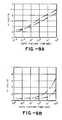
- Fig. 6is a graph which shows the relationship between the thickness of a gate oxide and the bit line disturb problem.
- Fig. 6shows the reduction in the charge (V t ), in volts, stored on the floating gate versus time for gate oxide thicknesses of 127 Angstroms, 160 Angstroms, and 200 Angstroms. From Fig. 6 it is clear that the bit line disturb problem depends on gate oxide thickness, and that a gate oxide thickness of 200 Angstroms or greater is required to prevent the bit line disturb problem.
- Fig. 7shows the self-limiting erase characteristics of a flash EPROM cell in accordance with the present invention, as compared with conventional devices.
- V tis plotted against time.
- Devices having floating gate actual doping levels of greater than 1x100cm ⁇ 3exhibit a continued removal of negative charges from the floating gate.
- a floating gate actual doping level of approximately 6.25x1018cm ⁇ 3limits the removal of negative charges from the floating gate at a voltage of -0.5 volts.
- a floating gate actual doping level of approximately 1.25x1018cm ⁇ 3, which is greater than the estimated optimum actual doping level of 5x1017cm ⁇ 3,provides the desired effect of limiting the removal of electron charges from the floating gate upon erasing.
- the graphclearly illustrates that the floating gate voltage V t continues to decrease well below 0 volts for the conventional device, whereas the floating gate voltage V t for a flash EPROM cell having an actual doping level of less than approximately 2x1018cm ⁇ 3' in accordance with the present invention, provides a self-limiting erase characteristic.
- Figs. 8A-Ccompare the hole current (I sub ) and gate or Fowler-Nordheim current (I G ) versus source voltage (V s ) for several structures.
- Fig. 8Arelates to a conventional structure without a double diffused source;
- Fig. 8Brelates to the structure of the first embodiment disclosed herein (Fig. 3);
- Fig. 8Crelates to the structures of the second and third embodiments of the present invention (Figs. 4 and 5).
- Fig. 8Ashows that a hole current is present for values of V s above approximately 3 volts in the conventional structure.
- the first embodiment of the present inventiondoes not exhibit a hole current until V s reaches approximately 5.5 volts, and the second and third embodiments of the present invention do not exhibit a hole current.
- I subequal to I G .
- the gate disturb characteristics of EPROM cells in accordance with the first embodimentare shown in Fig. 9A for erase voltage values of 10 volts (shown by the characters +) and 11 volts (shown by the characters x).
- Fig. 9BThe gate disturb characteristics of EPROM cells in accordance with the second and third embodiments are shown in Fig. 9B for erase voltage values of 10 volts (shown by the characters +) and 11 volts (shown by the characters x).
- the typical disturb time in high-density flash EPROM (1Mb)is less than one second.
- Fig. 9Ashows an approximate 1 volt change in V t whereas Fig. 9B only shows less than 0.1 volt change in V t .
Landscapes
- Engineering & Computer Science (AREA)
- Microelectronics & Electronic Packaging (AREA)
- Non-Volatile Memory (AREA)
- Semiconductor Memories (AREA)
- Bipolar Integrated Circuits (AREA)
- Bipolar Transistors (AREA)
Abstract
Description
- The present invention relates to one transistor flash EPROM memory cells.
- Flash EPROMs are a type of non-volatile memory which provides electrical erasing and a small cell size. The small cell size relates to the fact that each cell includes a single transistor. The term "flash" refers to the ability to rapidly erase the memory with electrical pulses. The erase operation erases an entire memory array, or at least large portion of the array -- single bits and/or bytes are not individually erasable.
- The flash EPROM cell includes a floating gate transistor which is programmed from the drain side by injecting hot electrons to the floating gate. Erasing can be accomplished from either the source or the drain side, with Fowler-Nordheim tunneling being the erase mechanism.
- Conventional flash EPROM cell structures are shown in Figs. 1 and 2. Conventional flash EPROMS, including those shown in Figs. 1 and 2, and the characteristics of same, are described in the following publications: (1) "A 128K Flash EPROM Using Double-Polysilicon Technology," Samachisa et al., IEEE Journal of Solid-State Circuits, Vol. SC-22, No. 5, October 1987; (2) "Corner-field Induced Drain Leakage In Thin Oxide Mosfets," Chi Chang and Jih Lien, Advanced Micro Devices, IEEE, IEDM 87, p.714; (3) "A Flash-Erase EEPROM Cell With An Asymmetric Source and Drain Structure," H. Kume et al., Central Research Laboratory, Hitachi Ltd., IEEE, IEDM 87, p. 560; (4) "An In-System Reprogrammable 256K CMOS Flash Memory," Virgil Niles Kynett et al., Intel Corporation, 1988 IEEE International Solid-State Circuits Conference; (5) "A High Density CMOS 1-T Electrically Erasable Non-Volatile (Flash) Memory Technology," S. Tam et al., Intel Corporation; (6) "Reliability Performance Of ETOX Based Flash Memories," Verma et al., Intel Corporation, 1988 IEEE/IRPS; (7) "A Single Transistor EEPROM Cell and Its Implementation in a 512K CMOS EEPROM," Mukherjee, et al., IEEE, IDEM 85, p.616; EP-A-0 182 198.
- The conventional flash EPROM cell shown in Fig. 1 includes a p-
type substrate 20, an n⁺-type drain 22 provided in thesubstrate 20, and a double diffused source having a first n⁻-type source region 24 and a second n⁺-type source region 26 inset infirst source region 24. Atunneling oxide 28 is provided on the surface of thesubstrate 20; thetunneling oxide 28 has a thickness of approximately 100 Angstroms (10 Angstroms = 1nm) to enable the tunneling type erase function to be performed. Apolysilicon floating gate 30 is provided on thetunneling oxide 28, and an inter-gate dielectric 32 separates floatinggate 30 fromcontrol gate 34. - The conventional flash EPROM shown in Fig. 2 includes a p-
type substrate 40 and n⁺-type source anddrain regions substrate 40. Atunnel oxide layer 46, having a thickness of approximately 200 Angstroms, is provided on the surface of thesubstrate 40 under afloating gate 48. Floatinggate 48 overlaps a portion of thedrain 42 and a portion of the channel. Dielectric 50 separates thefloating gate 48 fromcontrol gate 52 and a portion of thecontrol gate 52 is formed ongate oxide 46. This cell structure can be considered as two transistors in series; one transistor is the floating gate memory transistor and the other transistor is a series enhancement transistor controlled by the control gate. - In the flash EPROM cells shown in Figs. 1 and 2 the floating gate is heavily doped, the doping concentration is on the order of 10⁰cm⁻³, and thus a high level of built-in background electrons. The floating gates in those cells also have a thickness of approximately 2000 Angstroms, 1000 Angstroms in the most advanced technology.
- Programming a flash EPROM cell is usually accomplished by applying a relatively high voltage (approximately 12 volts) to the control gate and a moderately high voltage (approximately 9 volts) to the drain to generate hot electrons in the channel near the drain. The hot electrons are injected to the floating gate and trapped in the floating gate due to the fact that the floating gate is surrounded by insulators. The change in the threshold voltage, or channel conductance, of the cell created by the trapped hot electrons causes such a cell to be programmed, or charged.
- Erasing is accomplished by electron tunneling and/or hot-hole injection. For the structure in Fig. 1, a relatively high voltage (approximately 12 volts) is applied to the source of the cell while the gate is grounded, and the drain is usually floating. The electrons trapped in the floating gate flow toward and cluster at the portion of the floating gate overlying the n⁺-type source region and tunnel from the floating gate to the source due to the high electric field across the tunnel oxide.
- For the structure in Fig. 2, a voltage typically higher than 12 volts is applied to the drain of the cell while the gate is grounded and the source can be left either floating or grounded. Since the drain only includes an n⁺ region without an n⁻ diffusion, an appreciable number of hot holes are produced at the n⁺-p surface junction region by the so-called "avalanche effect." Hot holes can be injected from the surface junction to the floating gate and recombine with the trapped electrons, thereby assisting the erasure. If a relatively thick oxide is used as the tunnel oxide, electron tunneling is much less probable and hot-hole injection can actually become the dominant mechanism in erasing. However, it is well known that hot holes are easily captured by oxide traps. The trapped holes can cause serious degradation effect on oxide, namely, oxide charge leakage and early breakdown.
- The flash EPROM cells shown in Figs. 1 and 2 both suffer from the problem that electrical erasing is not self-limiting. Programming a flash EPROM cell involves providing negative charges on the floating gate. Erasing usually leaves the floating gate positively charged due to the tunnelling out of not only the electrons used to program the cell but also some of the built-in background electrons, possibly changing the transistor to a depletion-mode transistor. This is also true in the case of erasing by hot-hole injection.
- To prevent over-erasing in the cell structure shown in Fig. 1, an adaptive erase technique must be employed. Adaptive erasing uses complicated circuitry and software to perform a series of erase and verify steps. Each erase step performs only a portion of the erase function and the verify step is used to insure that the cell(s) are not over erased.
- Another problem associated with the flash EPROM cell shown in Fig. 1, is that the tunneling oxide thickness must be compromised. The tunneling oxide must be thin enough so that tunneling occurs during erasing, but thick enough so that tunneling is limited during the programming of the cell.
- A further problem with the flash EPROM cell structure shown in Fig. 1, is a phenomenon known as bit-line disturb, which causes the tunneling away of the stored charge during the programming of cells on the same bit line. In a memory array of flash EPROM cells, the drains of a group of cells are all connected to a bit line, whereas the control gates of the same group of cells are connected to separate word lines. Programming of individual cells is accomplished by applying the appropriate voltages to the bit line and a selected word line. The application of a voltage to the drain of cells which are not being programmed can cause Fowler-Nordheim tunneling or hot-hole injection, i.e., erasing, at the drain side of the device. The amount of unintentional erasing which occurs is a function of the gate oxide thickness and the length of time that the voltage is applied to the drain. In the structure shown in Fig. 1, where a thin tunneling dielectric 28 underlies the entire
floating gate 30, bit line disturb can be a serious problem. - In the structure shown in Fig. 2, erasing is the result of a combination of Fowler-Nordheim tunneling of electrons from the floating gate to the drain region and hot-hole injection from the surface n⁺-p junction to the floating gate. Adaptive erasing is not used to prevent over-erasing; instead the series enhancement transistor is used to prevent current flow when the memory transistor is placed in the depletion-mode. Particularly, the series enhancement transistor prevents leakage current which occurs in a memory array during programming and/or reading due to an over-erased cell. Although adaptive erasing is not required with the cell structure shown in Fig. 2, the cell structure is approximately 20% larger than the cell shown in Fig. 1 due to the added gate width of the control gate.
- The relatively
thick gate oxide 46 underlyingfloating gate 48 makes bit line disturb less of a problem than with the Fig. 1 structure. Nevertheless, in the Fig. 2 structure, a tradeoff is still necessary, in that thegate oxide 46 must be thin enough so that tunneling occurs during erasing. It can be shown that with a gate oxide thickness greater than 125 Angstroms hot hole injection due to surface junction breakdown can dominate over tunnelling. The drawback of the structure in Fig. 2 is that programming and erasing both are done at the drain side. As a result, the oxide thickness and junction structure cannot be optimized for programming or erasing independently. - In conventional flash EPROM cells, when the erase voltage Vpp is applied to the source during erasing, the surface of an n⁺ source is depleted in the n+-gate overlap region. This surface depletion creates a high surface field, which in turn causes band-to-band tunnelling. Band-to-band tunnelling generates holes in an n⁺ source, and the holes tend to flow to the p-type substrate. The flow of holes to the p-type substrate maintains the surface depletion of the n⁺ source, thereby increasing the effective thickness of the dielectric. The increase in the effective thickness of dielectric makes tunnelling more difficult.
- Another disadvantage of having a band-to-band tunneling current is that it is not feasible to design a charge-pumping circuit to generate the high voltage used for erasing. Typically, the hole current which flows to the substrate is on the order of 0.1 micro-amps per cell at its peak. For a memory chip of 256K density level, for example, a chip erase can generate as high a substrate current as 25 milli-amps, which cannot be handled by a conventional charge pump. The excessive amount of substrate current produced during erase can prevent the realization of Flash memories successfully implemented in a 5-volt system in the future.
- Holes which flow from the n⁺ surface to the substrate can gain energy from the electric field when crossing the n⁺-p surface-junction depletion region. Some of the holes become sufficiently hot to be injected into the oxide, as discussed earlier.
- A problem with the generation of hot holes is that holes which are trapped in the tunnel oxide during erasing have the effect of reducing the barrier for electron tunnelling, thereby increasing low-level leakages. The low-level oxide leakage can cause erased cells on the same word line to become partially programmed during the programming of other cells on the same word line, a problem termed gate (or word-line) disturb.
- Other types of EPROMs are known from EP-A-0 183 235 and EP-A-0 204 498.
- The improved floating gate transistor to be described is for use in a flash EPROM cell.
- The flash EPROM cell has a self-limiting erase characteristics, and is not subject to bit line disturb or gate disturb.
- The cell has a multi-thickness dielectric provided between the substrate and the floating gate, the multi-thickness dielectric having a tunneling dielectric portion overlapping the source, and a gate oxide portion overlapping the drain.
- The cell also has a semi-insulating floating gate. A semi-insulating gate has a low concentration of built-in background electrons, so that erasing ceases when substantially all of the injected electrons are tunnelled out of the floating gate, returning the cell to its unprogrammed state without removing built-in background electrons. Therefore, the erase operation does not create positive charges on the floating gate, and an enhancement mode device will not be converted to a depletion mode device by the erase operation.
- A one transistor flash EPROM cell embodying the present invention is defined in appended
claim 1. - Fig. 1 is a partial, cross-sectional view of a conventional one transistor flash EPROM cell;
- Fig. 2 is a partial, cross-sectional view of another conventional one transistor flash EPROM cell;
- Fig. 3 is a partial, cross-sectional view of a first embodiment of a one transistor flash EPROM cell in accordance with the present invention;
- Fig. 4 is a partial, cross-sectional view of a second embodiment of a one transistor flash EPROM cell in accordance with the present invention;
- Fig. 5 is a partial, cross-sectional view of a third embodiment of a one transistor flash EPROM ceil in accordance with the present invention;
- Fig. 6 is a graph for explaining the relationship between gate oxide thickness and the bit line disturb problem;
- Fig. 7 is a graph for explaining the self-limiting erase characteristics of one transistor flash EPROM cells in accordance with the present invention;
- Figs. 8A-C are graphs illustrating the prevention of hole current generation in the flash EPROM cells of the present invention; and
- Figs. 9A and B are graphs showing that flash EPROM cells in accordance with the present invention are resistant to the gate disturb problem.
Flash EPROM cells - As shown in Fig. 3, a one transistor
flash EPROM cell 90 in accordance with the present invention comprises asubstrate 100 having,source 102 and drain 104 regions provided therein.Source 102 and drain 104 are spaced apart to define achannel 105 therebetween. Thesubstrate 100 is usually a p-type semiconductor withsource 102 and drain 104 being n-type regions; however, it is possible to build a one transistor flash EPROM cell having opposite conductivity types from those described herein, or to build the devices described herein in a p-well provided in an n-type substrate. Accordingly, the description of the preferred embodiments of the present invention are not intended to limit the invention to particularly conductivity types. Source 102 has a double diffused structure, including a first n⁻-type source region 106 and a second n⁺-type source region 108 provided infirst source region 106.Drain region 104 has n⁺-type conductivity. The doping level for n⁻source 106 is approximately 1x10¹⁹cm⁻³, and the doping level for n⁺source 108 and n⁺drain 104 is approximately 3x10⁰cm⁻³.- A multi-thickness dielectric layer 110, provided on the surface of
substrate 100, includes a tunnelling dielectric region 111 and agate oxide region 112. As used herein, "multi-thickness" refers to the characteristic that at least two portions of the dielectric have different physical or effective thicknesses. Effective thickness refers to changes in the tunneling characteristics of a dielectric due to factors other than physical thickness, for example, the type of dielectric material, the electric field applied across the dielectric, and/or any effects such as an intentional depletion of the source or drain which changes the tunnelling characteristics of the dielectric. Thus, the tunnelling dielectric 111 and thegate oxide 112 may have different thicknesses, or may be formed of different materials having the same thickness. Alternatively, the multi-thickness dielectric 110 may be formed of two portions of the same material having the same thickness but different effective thicknesses. - Multi-thickness dielectric 110 serves several purposes, including the elimination of the need to compromise on the thickness of the oxide layer to provide a balance between the functions of a tunnelling dielectric and a gate oxide. Tunnelling dielectric 111, provided on the source side of the device, allows tunnelling to occur during the erase operation;
gate oxide 112, provided at the drain side of the device, prevents tunnelling during programming and eliminates or reduces the bit line disturb problem associated with conventional flash EPROMs. Tunnelling dielectric 111 is less than 150 Angstroms thick, with the preferred thickness ranging from 80 to 110 Angstroms.Gate oxide 112 has a thickness which is greater than approximately 200 Angstroms. - An additional benefit of the
thick gate oxide 112 is that the drain junction breakdown voltage is increased so that very few hot holes are generated. Preventing the generation of hot holes is useful in eliminating the loss of charge in unselected cells on the same bit line as a cell being programmed. Sincesource 102 is at ground potential during programming, tunnelling does not occur from the floatinggate 114 to thesource 102 during programming. On the other hand, the thin tunnelling dielectric 111 is desirable to facilitate tunnelling at the source side of the cell during erasing. - Floating
gate 114 is provided on multi-thickness dielectric 110. The floatinggate 114 is formed of a semi-insulating material, for example, lightly doped polysilicon, which has very few built-in background. free electrons. In particular, the background electron concentration in the unprogrammed state is far less than the injected electron concentration of the programmed state. Since floatinggate 114 is a semi-insulating material, the so-called capacitive coupling effect either does not exist or is quite small. Therefore, the floatinggate 114 can be considered as portion of the dielectric 110; however, floatinggate 114 is sufficiently conductive so that injected electrons can re-distribute themselves with a relaxation time of less than 1µs. The semi-insulating characteristic of floatinggate 114 is provided by, for example, forming the floatinggate 114 with polysilicon having an actual doping level of approximately 5x10¹⁷cm⁻³. The term "actual doping level" refers to the density of donor dopants introduced, e.g., implanted, into the material of floatinggate 114. The polycrystalline characteristics of polysilicon prevent the activation of many dopants which are introduced, and, in general, only one percent (1%) of implanted dopants are activated -- activation of implanted dopants is usually accomplished by annealing. The desired activated carrier concentration for apolysilicon floating gate 114 is approximately 1x10¹⁶cm⁻³. - It is well known that the resistivity of a polysilicon film (or layer) is a function of the film deposition technology and the thermal cycles to which the polysilicon film is subjected. The film resistivity is determined by the number of built-in electrons and their mobilities in the polysilicon film. Thus the actual doping levels set forth herein are related to the stated fabrication techniques and equivalents thereof. If alternate deposition technologies are employed the actual doping level should be varied to provide an activated carrier concentration of less than 1x10¹⁶cm⁻³.
- An
inter-gate dielectric 116separates floating gate 114 andcontrol gate 118, with the floatinggate 114,inter-gate dielectric 116 andcontrol gate 118 forminggate structure 119. - The coupling effect of semi-insulating floating
gate 114 is very weak and floatinggate 114 essentially behaves as an insulator before thecell 90 is programmed. Therefore, floatinggate 114 must be relatively thin so that the channel conductance is controlled by the voltage applied to controlgate 118. In the present invention, the floatinggate 114 is less than approximately 1000 Angstroms in thickness. - A further benefit of the semi-insulating floating
gate 114 is that the electric field of unselected (or erased) cells on the same word line as a cell being programmed is decreased during programming of other cells on the same word line due to the increase in the effective thickness ofgate oxide 112. On the other hand, a small penalty is associated with the use of a semi-insulating floatinggate 114, in that the core gain is reduced; specifically, there is a reduction in the channel current during reading of thecell 90. This reduction in the channel current can be overcome by increasing the width of the transistor. Thus, the area of a flash EPROM cell in accordance with the present invention is approximately 25% larger than the area of the conventional flash EPROM cell shown in Fig. 1 and approximately equal to the area of the conventional flash EPROM cell shown in Fig. 2. - The
flash EPROM cell 90 of the first embodiment of the present invention is fabricated in the following manner. First,field oxide regions 120 are formed onsubstrate 100 to separate the areas where multiple flash EPROM cells will be formed on a single substrate. An oxide layer is grown on the surface of thesubstrate 100 and the portion of the oxide layer which is to become gate oxide 110 is masked. The remaining portion of the oxide layer is removed, and tunnelling dielectric 111 is then grown. Thegate structure 119, including floatinggate 114, inter-gate dielectric 116 (usually silicon oxide, or a combination of silicon oxide and nitride) andcontrol gate 118, is formed on dielectric layer 110. In accordance with conventional manufacturing techniques the various elements of thegate structure 119 are formed as continuous layers and then etched to achieve the final structure. - After the
gate structure 119 is formed, n⁻source 106 is formed by implanting a light dose of an n-type dopant, e.g., phosphorus ions, with an energy ranging from 50-75KeV, and driving the implanted ions with a thermal cycle. N⁺drain 104 and n⁺source 108 are then implanted with an energy ranging from 50-70KeV and thermally driven. Since thegate structure 119 is formed prior to implantingsource 102 and drain 104,source 102 and drain 104 are self-aligned with thegate structure 119. - With reference to Fig. 4, a flash EPROM cell in accordance with the second embodiment of the present invention is also formed in a portion of a
substrate 100 isolated byfield oxide regions 120. N⁺drain region 104 and doublediffused source 122 are provided in the substrate, withsource 122 and drain 104 defining achannel 123 therebetween.Source 122 includes a first, n⁻source region 124 and a second, n⁺source region 126. The doping level for n⁻source 124 is approximately 1x10¹⁹cm⁻³, and the doping level for n⁺source 126 and n⁺drain 104 is approximately 3x10⁰cm⁻³. Source 122 of the second embodiment differs fromsource 102 of the first embodiment, in that n⁻source 124 is not self-aligned with thegate structure 127 and extends further under thegate structure 127. Thesecond source region 126, however, is self-aligned with thegate structure 127.- A
multi-thickness dielectric 128, including atunnelling dielectric 130 and agate oxide 132, is provided on the surface ofsubstrate 100. In this second embodiment of the invention,gate oxide 132 is formed on portions ofsubstrate 100 which overlapdrain 104,channel 123, and a first portion 124a of n⁻source 124.Tunnelling dielectric 130 is formed on a portions of the surface ofsubstrate 100 corresponding to the position of asecond portion 124b of n⁻source 124 and a portion of n⁺source 126. Thegate structure 127 of the second embodiment, which is similar to thegate structure 119 in the first embodiment, includes semi-insulating floatinggate 134,inter-gate dielectric 136, andcontrol gate 138.Semi-insulating gate 134 has an activated carrier concentration of less than approximately 1x10¹⁶cm⁻³ and a thickness of less than 1000 Angstroms. - The overlap of
gate oxide 132 and a portion of n⁻source 124 suppresses hot hole generation during erasing and creates an energy barrier to the flow of holes into thesubstrate 100. Thus, the gate disturb problem is prevented and erase tunnelling is facilitated by the prevention of continuous hole generation and the collapse of the surface depletion layer. Further, since the generation of holes is prevented, only a negligible hole current will flow to the substrate. - The fabrication of a flash EPROM cell in accordance with the second embodiment of the present invention includes the following steps. First, an oxide is grown on the surface of
substrate 100. The portion of the oxide outside of the tunnelling region, comprisinggate oxide 132, is masked for the implantation of phosphorus or arsenic ions to form n⁻source 124. The portion of the oxide exposed to the implantation is removed by etching.Tunnel dielectric 130 is then grown on the surface ofsubstrate 100, completing the formation ofmulti-thickness dielectric 128. Thegate structure 127 is formed onmulti-thickness dielectric 128, and then used as a mask to implant self-aligned n⁺drain 104 and n⁺source 126. The doping levels and implant energies are approximately the same as those utilized in the fabrication of a flash EPROM cell in accordance with the first embodiment. - In the third embodiment of a flash EPROM cell in accordance with the present invention, shown in Fig. 5, a p⁻-type substrate 139 is used and the
drain region 140 includes a p-type region implanted into substrate 139. In addition, thedrain 140 has a double diffused structure including a first, n⁻-type drain region 144 and a second, n⁺-type drain region 146 provided in n⁻ drain 144.Source region 148 includes a first, n⁻-type region 150 and a second, n⁺-type 152 provided in n⁻-type region 150. The doping level for n⁻source 150 is approximately 2x10¹⁹cm⁻³, and the doping level for n⁺source 152 is approximately 3x10⁰cm⁻³. The doping level for n⁻ drain 144 is approximately 2x10¹⁹cm⁻³, and the doping level for n⁺drain 146 is approximately 3x10⁰cm⁻³. The implant energies are as follows: n⁻ drain 144, 60KeV; n⁺drain 146, 50KeV; n⁻source 150, 60KeV; and n⁺source 152, 50KeV. - A
multi-thickness dielectric 154, includinggate oxide 158 andtunnelling dielectric 156, is provided on the surface of substrate 139.Gate structure 159, provided ondielectric 154, is similar to that of the first and second embodiments, includingsemi-insulating floating gate 160,inter-gate dielectric 162, andcontrol gate 164. The attributes ofmulti-thickness dielectric 154 and the elements ofgate structure 159, including floatinggate 160, are similar to those of corresponding elements in the first and second embodiments. - In the second embodiment, the
channel region 123 formed betweendrain 104 andfirst source region 124 is not self-aligned because n⁻source 124 is implanted before thegate structure 127 is formed. To provide self-aligned elements, the method of fabricating a flash EPROM cell in accordance with the third embodiment of the present invention is as follows. First, the substrate is masked and p-type region 142 is implanted. The substrate is then re-masked and n⁻-type regions gate oxide 158 remains.Tunnelling dielectric 156 is then grown on the surface of substrate 139, completing the formation ofmulti-thickness dielectric 154.Gate structure 159 is formed onmulti-thickness dielectric 154, and, subsequently, n⁺drain region 146 and n⁺source region 152 are implanted. - Fig. 6 is a graph which shows the relationship between the thickness of a gate oxide and the bit line disturb problem. In particular, Fig. 6 shows the reduction in the charge (Vt), in volts, stored on the floating gate versus time for gate oxide thicknesses of 127 Angstroms, 160 Angstroms, and 200 Angstroms. From Fig. 6 it is clear that the bit line disturb problem depends on gate oxide thickness, and that a gate oxide thickness of 200 Angstroms or greater is required to prevent the bit line disturb problem.
- Fig. 7 shows the self-limiting erase characteristics of a flash EPROM cell in accordance with the present invention, as compared with conventional devices. In Fig. 7 Vt is plotted against time. Devices having floating gate actual doping levels of greater than 1x10⁰cm⁻³ exhibit a continued removal of negative charges from the floating gate. A floating gate actual doping level of approximately 6.25x10¹⁸cm⁻³ limits the removal of negative charges from the floating gate at a voltage of -0.5 volts. A floating gate actual doping level of approximately 1.25x10¹⁸cm⁻³, which is greater than the estimated optimum actual doping level of 5x10¹⁷cm⁻³, provides the desired effect of limiting the removal of electron charges from the floating gate upon erasing. The graph clearly illustrates that the floating gate voltage Vt continues to decrease well below 0 volts for the conventional device, whereas the floating gate voltage Vt for a flash EPROM cell having an actual doping level of less than approximately 2x10¹⁸cm⁻³' in accordance with the present invention, provides a self-limiting erase characteristic.
- Figs. 8A-C compare the hole current (Isub) and gate or Fowler-Nordheim current (IG) versus source voltage (Vs) for several structures. Fig. 8A relates to a conventional structure without a double diffused source; Fig. 8B relates to the structure of the first embodiment disclosed herein (Fig. 3); and Fig. 8C relates to the structures of the second and third embodiments of the present invention (Figs. 4 and 5). Fig. 8A shows that a hole current is present for values of Vs above approximately 3 volts in the conventional structure. The first embodiment of the present invention does not exhibit a hole current until Vs reaches approximately 5.5 volts, and the second and third embodiments of the present invention do not exhibit a hole current. In particular, in structures in accordance with the second and third embodiments of the present invention Isub equal to IG.
- Figs. 9A and B show the resistance of the flash EPROM cells of the present invention to the gate disturb problem, by plotting the threshold voltage Vt versus time. It is noted that although the graphs plot Vt, if it is assumed that Vt is zero volts at t=10⁻³ seconds the voltage shown is the change in voltage. Fig. 9A shows Vt as 0.5 volts at t=10⁻³s, and thus the change in voltage can be calculated by subtracting 0.5volts from all values of Vt. The gate disturb characteristics of EPROM cells in accordance with the first embodiment are shown in Fig. 9A for erase voltage values of 10 volts (shown by the characters +) and 11 volts (shown by the characters x). The gate disturb characteristics of EPROM cells in accordance with the second and third embodiments are shown in Fig. 9B for erase voltage values of 10 volts (shown by the characters +) and 11 volts (shown by the characters x). The typical disturb time in high-density flash EPROM (1Mb) is less than one second. At one second, Fig. 9A shows an approximate 1 volt change in Vt whereas Fig. 9B only shows less than 0.1 volt change in Vt.
Claims (9)
- An electrically programmable and erasable semiconductor device, comprising: a substrate (100) having a source region (102, 122, 148) spaced from a drain region (104, 140) by a channel region (105, 123, 165); a control gate (118, 138, 164) and a floating gate (114, 134, 160) separated by an inter-gate dielectric (116, 136, 162), the floating gate being semi-insulating whereby the floating gate essentially acts as an insulator in the unprogrammed state; and dielectric means (110, 128, 154) on the substrate (100) to allow tunnelling during erasing, the dielectric means (110, 128, 154) including a first tunnelling dielectric portion (111, 130, 156) disposed at least partially over the source region (102, 122, 148) and a second gate oxide portion (112, 132, 158) disposed at least partially over the channel region (105, 123, 165) and overlapping the drain region (104, 140), the first tunnelling dielectric portion having a smaller effective thickness than the second gate oxide portion.
- A semiconductor device according to claim 1 wherein the second gate oxide portion (112, 113, 158) of the dielectric means (110, 128, 154) has a greater physical thickness than the first tunnelling dielectric portion (111, 130, 156).
- A semiconductor device according to claim 1 or claim 2 wherein the source region (102, 122, 148) comprises a first lightly doped source region (106, 124, 150) in the substrate (100) and a second heavily doped source region (108, 126, 152) in the first source region, the first tunnelling portion (111, 130, 156) of the dielectric means overlapping both the first source region and the second source region.
- A semiconductor device according to any one of the preceding claims, wherein the floating gate (114, 134, 160) has a thickness of less than 100nm (1000Å) and an actual doping level of less than 5x10¹⁸cm⁻³.
- A semiconductor device according to any one of claims 1-3, wherein the floating gate (114, 134, 160) has a thickness of less than 100nm (1000Å) and an activated carrier concentration of less than 1x10¹⁷cm⁻³.
- A semiconductor device according to claim 2, wherein:the first tunnelling portion (111, 130, 156) of the dielectric means (110, 128, 154) has a thickness of less than approximately 15nm (150Å); andthe second gate portion (112, 132, 158) of the dielectric means (110, 128, 154) has a thickness of greater than approximately 20nm (200Å).
- A semiconductor device according to any one of the preceding claims wherein the device is a flash EPROM cell having self-limiting erase characteristics, and wherein the second portion (112, 132, 158) of the dielectric means additionally provides an energy barrier to the flow of holes into the substrate (100); the floating gate (114, 134, 160) having a doping level sufficient only to allow injected electrons to redistribute during the programming of the EPROM cell.
- A semiconductor device according to any one of the preceding claims wherein the device is a one transistor flash EPROM cell and wherein the drain region (140) includes a first drain region (144) in the substrate (100) and a second drain region (146) in said first drain region, said second drain region (146) having a greater doping level than said first drain region (144).
- A semiconductor device according to claim 1 wherein the device is a one transistor flash EPROM cell and wherein the substrate (100) is a p-type substrate, the drain region (140) comprises an n⁻-type drain region (144) in the substrate (100) and an n⁺-type drain region (146) in the n⁻-type drain region (144); and the source region (148) comprises an n⁻-type source region (150) in the substrate (100), and an n⁺-type source region (152) in the n⁻-type source region (150).
Applications Claiming Priority (2)
| Application Number | Priority Date | Filing Date | Title |
|---|---|---|---|
| US247887 | 1988-09-22 | ||
| US07/247,887US4958321A (en) | 1988-09-22 | 1988-09-22 | One transistor flash EPROM cell |
Publications (3)
| Publication Number | Publication Date |
|---|---|
| EP0360504A2 EP0360504A2 (en) | 1990-03-28 |
| EP0360504A3 EP0360504A3 (en) | 1990-10-31 |
| EP0360504B1true EP0360504B1 (en) | 1996-04-10 |
Family
ID=22936796
Family Applications (1)
| Application Number | Title | Priority Date | Filing Date |
|---|---|---|---|
| EP89309382AExpired - LifetimeEP0360504B1 (en) | 1988-09-22 | 1989-09-15 | One transistor flash eprom cell |
Country Status (5)
| Country | Link |
|---|---|
| US (1) | US4958321A (en) |
| EP (1) | EP0360504B1 (en) |
| JP (1) | JPH02135783A (en) |
| AT (1) | ATE136688T1 (en) |
| DE (1) | DE68926205T2 (en) |
Families Citing this family (63)
| Publication number | Priority date | Publication date | Assignee | Title |
|---|---|---|---|---|
| US5262987A (en)* | 1988-11-17 | 1993-11-16 | Seiko Instruments Inc. | Floating gate semiconductor nonvolatile memory having impurity doped regions for low voltage operation |
| US5844842A (en)* | 1989-02-06 | 1998-12-01 | Hitachi, Ltd. | Nonvolatile semiconductor memory device |
| US6373093B2 (en) | 1989-04-28 | 2002-04-16 | Nippondenso Corporation | Semiconductor memory device and method of manufacturing the same |
| US5017979A (en)* | 1989-04-28 | 1991-05-21 | Nippondenso Co., Ltd. | EEPROM semiconductor memory device |
| JPH02308571A (en)* | 1989-05-24 | 1990-12-21 | Toshiba Corp | Semiconductor memory device |
| US5077691A (en)* | 1989-10-23 | 1991-12-31 | Advanced Micro Devices, Inc. | Flash EEPROM array with negative gate voltage erase operation |
| US5126808A (en)* | 1989-10-23 | 1992-06-30 | Advanced Micro Devices, Inc. | Flash EEPROM array with paged erase architecture |
| US5122985A (en)* | 1990-04-16 | 1992-06-16 | Giovani Santin | Circuit and method for erasing eeprom memory arrays to prevent over-erased cells |
| JPH0456283A (en)* | 1990-06-25 | 1992-02-24 | Matsushita Electron Corp | Semiconductor memory device and manufacture thereof |
| US5032881A (en)* | 1990-06-29 | 1991-07-16 | National Semiconductor Corporation | Asymmetric virtual ground EPROM cell and fabrication method |
| US5222040A (en)* | 1990-12-11 | 1993-06-22 | Nexcom Technology, Inc. | Single transistor eeprom memory cell |
| US5197027A (en)* | 1991-01-24 | 1993-03-23 | Nexcom Technology, Inc. | Single transistor eeprom architecture |
| US5345418A (en)* | 1991-01-24 | 1994-09-06 | Nexcom Technology, Inc. | Single transistor EEPROM architecture |
| JP2793722B2 (en)* | 1991-01-29 | 1998-09-03 | 富士通株式会社 | Nonvolatile semiconductor memory device and method of manufacturing the same |
| US5191556A (en)* | 1991-03-13 | 1993-03-02 | Advanced Micro Devices, Inc. | Method of page-mode programming flash eeprom cell arrays |
| US5424567A (en)* | 1991-05-15 | 1995-06-13 | North American Philips Corporation | Protected programmable transistor with reduced parasitic capacitances and method of fabrication |
| US5130769A (en)* | 1991-05-16 | 1992-07-14 | Motorola, Inc. | Nonvolatile memory cell |
| US5264384A (en)* | 1991-08-30 | 1993-11-23 | Texas Instruments Incorporated | Method of making a non-volatile memory cell |
| JP3431647B2 (en) | 1992-10-30 | 2003-07-28 | 株式会社半導体エネルギー研究所 | Semiconductor device, method for manufacturing same, method for manufacturing memory device, and method for laser doping |
| DE69325442T2 (en)* | 1993-03-18 | 1999-12-16 | Stmicroelectronics S.R.L., Agrate Brianza | Non-volatile flash EEPROM memory device |
| US5349225A (en)* | 1993-04-12 | 1994-09-20 | Texas Instruments Incorporated | Field effect transistor with a lightly doped drain |
| US5343424A (en)* | 1993-04-16 | 1994-08-30 | Hughes Aircraft Company | Split-gate flash EEPROM cell and array with low voltage erasure |
| BE1007475A3 (en)* | 1993-09-06 | 1995-07-11 | Philips Electronics Nv | Semiconductor device having a non-volatile memory and method for fabricating such a semiconductor device. |
| US5432749A (en)* | 1994-04-26 | 1995-07-11 | National Semiconductor Corporation | Non-volatile memory cell having hole confinement layer for reducing band-to-band tunneling |
| US5416738A (en)* | 1994-05-27 | 1995-05-16 | Alliance Semiconductor Corporation | Single transistor flash EPROM cell and method of operation |
| US5468981A (en)* | 1994-09-01 | 1995-11-21 | Advanced Micro Devices, Inc. | Self-aligned buried channel/junction stacked gate flash memory cell |
| US5574685A (en)* | 1994-09-01 | 1996-11-12 | Advanced Micro Devices, Inc. | Self-aligned buried channel/junction stacked gate flash memory cell |
| US5801076A (en)* | 1995-02-21 | 1998-09-01 | Advanced Micro Devices, Inc. | Method of making non-volatile memory device having a floating gate with enhanced charge retention |
| US5581502A (en)* | 1995-05-02 | 1996-12-03 | Advanced Micro Devices, Inc. | Method for reading a non-volatile memory array |
| US5648669A (en)* | 1995-05-26 | 1997-07-15 | Cypress Semiconductor | High speed flash memory cell structure and method |
| US5546340A (en)* | 1995-06-13 | 1996-08-13 | Advanced Micro Devices, Inc. | Non-volatile memory array with over-erase correction |
| US6787844B2 (en) | 1995-09-29 | 2004-09-07 | Nippon Steel Corporation | Semiconductor device including transistor with composite gate structure and transistor with single gate structure, and method for manufacturing the same |
| US5811334A (en)* | 1995-12-29 | 1998-09-22 | Advanced Micro Devices, Inc. | Wafer cleaning procedure useful in the manufacture of a non-volatile memory device |
| US6236597B1 (en) | 1996-09-16 | 2001-05-22 | Altera Corporation | Nonvolatile memory cell with multiple gate oxide thicknesses |
| US5889700A (en)* | 1997-05-05 | 1999-03-30 | National Semiconductor Corporation | High density EEPROM array using self-aligned control gate and floating gate for both access transistor and memory cell and method of operating same |
| US6451686B1 (en)* | 1997-09-04 | 2002-09-17 | Applied Materials, Inc. | Control of semiconductor device isolation properties through incorporation of fluorine in peteos films |
| US5972749A (en)* | 1998-01-05 | 1999-10-26 | Advanced Micro Devices, Inc. | Method for preventing P1 punchthrough |
| US6743688B1 (en)* | 1998-01-05 | 2004-06-01 | Advanced Micro Devices, Inc. | High performance MOSFET with modulated channel gate thickness |
| US5998262A (en)* | 1998-04-23 | 1999-12-07 | Worldwide Semiconductor Manufacturing Corp. | Method for manufacturing ETOX cell having damage-free source region |
| US6140676A (en)* | 1998-05-20 | 2000-10-31 | Cypress Semiconductor Corporation | Semiconductor non-volatile memory device having an improved write speed |
| US6512401B2 (en)* | 1999-09-10 | 2003-01-28 | Intel Corporation | Output buffer for high and low voltage bus |
| EP1120836A1 (en)* | 2000-01-28 | 2001-08-01 | STMicroelectronics S.r.l. | Memory cell structure integrated on semiconductor |
| US6277691B1 (en)* | 2000-04-04 | 2001-08-21 | Chartered Semiconductor Manufacturing Ltd. | Method to fabricate a robust and reliable memory device |
| US6750157B1 (en) | 2000-10-12 | 2004-06-15 | Advanced Micro Devices, Inc. | Nonvolatile memory cell with a nitridated oxide layer |
| US20020123180A1 (en)* | 2001-03-01 | 2002-09-05 | Peter Rabkin | Transistor and memory cell with ultra-short gate feature and method of fabricating the same |
| KR100471165B1 (en)* | 2002-05-07 | 2005-03-08 | 삼성전자주식회사 | Nonvolatile Memory Device With Non-planar Gate-Insulating Layer And Method Of Fabricating The Same |
| DE10224956A1 (en)* | 2002-06-05 | 2004-01-08 | Infineon Technologies Ag | Process for setting the threshold voltage of a field effect transistor, field effect transistor and integrated circuit |
| US20040061190A1 (en)* | 2002-09-30 | 2004-04-01 | International Business Machines Corporation | Method and structure for tungsten gate metal surface treatment while preventing oxidation |
| US6760270B2 (en)* | 2002-09-30 | 2004-07-06 | Motorola, Inc. | Erase of a non-volatile memory |
| US6906529B2 (en)* | 2003-06-10 | 2005-06-14 | Stmicroelectronics, Inc. | Capacitive sensor device with electrically configurable pixels |
| KR100552839B1 (en)* | 2003-11-05 | 2006-02-22 | 동부아남반도체 주식회사 | Semiconductor device and manufacturing method thereof |
| KR100666615B1 (en)* | 2004-04-14 | 2007-01-09 | 매그나칩 반도체 유한회사 | Flash memory devices |
| KR100731058B1 (en)* | 2005-12-26 | 2007-06-22 | 동부일렉트로닉스 주식회사 | Flash memory cell comprising a double tunnel oxide film and a method of manufacturing the same |
| WO2008067494A1 (en)* | 2006-11-29 | 2008-06-05 | Rambus Inc. | Integrated circuit with built-in heating circuitry to reverse operational degeneration |
| JP2011100876A (en)* | 2009-11-06 | 2011-05-19 | Asahi Kasei Electronics Co Ltd | P-channel nonvolatile memory and semiconductor device, and method of manufacturing p-channel nonvolatile memory |
| CN102184896B (en)* | 2011-04-06 | 2012-08-29 | 北京大学 | Technique method for restraining flash memory programming interference |
| KR101334844B1 (en)* | 2011-12-29 | 2013-12-05 | 주식회사 동부하이텍 | Single poly eeprom and method for fabricating the same |
| US8658495B2 (en)* | 2012-03-08 | 2014-02-25 | Ememory Technology Inc. | Method of fabricating erasable programmable single-poly nonvolatile memory |
| US9899485B2 (en)* | 2016-06-07 | 2018-02-20 | International Business Machines Corporation | Spatially decoupled floating gate semiconductor device |
| CN106992174B (en)* | 2017-01-18 | 2019-04-19 | 南方科技大学 | transistor memory |
| FR3071355B1 (en) | 2017-09-20 | 2019-08-30 | Stmicroelectronics (Rousset) Sas | MEMORY CELL-COMPACT EEPROM |
| US11362188B2 (en)* | 2017-12-27 | 2022-06-14 | Intel Corporation | Field effect transistors with reduced electric field by thickening dielectric on the drain side |
| CN111968983B (en)* | 2019-05-20 | 2023-10-17 | 联华电子股份有限公司 | Structure of memory element and manufacturing method thereof |
Citations (1)
| Publication number | Priority date | Publication date | Assignee | Title |
|---|---|---|---|---|
| EP0182198A2 (en)* | 1984-11-21 | 1986-05-28 | Rohm Corporation | Single transistor electrically programmable device and method |
Family Cites Families (8)
| Publication number | Priority date | Publication date | Assignee | Title |
|---|---|---|---|---|
| US4267588A (en)* | 1978-12-07 | 1981-05-12 | Alexander Daniels | Hourglass construction |
| US4409723A (en)* | 1980-04-07 | 1983-10-18 | Eliyahou Harari | Method of forming non-volatile EPROM and EEPROM with increased efficiency |
| DE3587615D1 (en)* | 1984-11-26 | 1993-11-11 | Toshiba Kawasaki Kk | Non-volatile semiconductor memory device. |
| US4811078A (en)* | 1985-05-01 | 1989-03-07 | Texas Instruments Incorporated | Integrated circuit device and process with tin capacitors |
| EP0204498A3 (en)* | 1985-05-29 | 1988-09-21 | Advanced Micro Devices, Inc. | Improved eeprom cell and method of fabrication |
| JPS62150782A (en)* | 1985-12-25 | 1987-07-04 | Hitachi Ltd | Method for manufacturing semiconductor integrated circuit device |
| JPS63144577A (en)* | 1986-12-09 | 1988-06-16 | Toshiba Corp | Non-volatile semiconductor memory device |
| JPH01289282A (en)* | 1988-05-17 | 1989-11-21 | Ricoh Co Ltd | Semiconductor memory device |
- 1988
- 1988-09-22USUS07/247,887patent/US4958321A/ennot_activeExpired - Lifetime
- 1989
- 1989-09-15ATAT89309382Tpatent/ATE136688T1/ennot_activeIP Right Cessation
- 1989-09-15DEDE68926205Tpatent/DE68926205T2/ennot_activeExpired - Fee Related
- 1989-09-15EPEP89309382Apatent/EP0360504B1/ennot_activeExpired - Lifetime
- 1989-09-18JPJP1241654Apatent/JPH02135783A/enactivePending
Patent Citations (1)
| Publication number | Priority date | Publication date | Assignee | Title |
|---|---|---|---|---|
| EP0182198A2 (en)* | 1984-11-21 | 1986-05-28 | Rohm Corporation | Single transistor electrically programmable device and method |
Also Published As
| Publication number | Publication date |
|---|---|
| JPH02135783A (en) | 1990-05-24 |
| EP0360504A3 (en) | 1990-10-31 |
| ATE136688T1 (en) | 1996-04-15 |
| DE68926205T2 (en) | 1996-11-28 |
| US4958321A (en) | 1990-09-18 |
| DE68926205D1 (en) | 1996-05-15 |
| EP0360504A2 (en) | 1990-03-28 |
Similar Documents
| Publication | Publication Date | Title |
|---|---|---|
| EP0360504B1 (en) | One transistor flash eprom cell | |
| US6326265B1 (en) | Device with embedded flash and EEPROM memories | |
| US5838041A (en) | Nonvolatile semiconductor memory device having memory cell transistor provided with offset region acting as a charge carrier injecting region | |
| US5824584A (en) | Method of making and accessing split gate memory device | |
| EP0974146B1 (en) | Nonvolatile memory | |
| US7057931B2 (en) | Flash memory programming using gate induced junction leakage current | |
| US6760258B2 (en) | Means to erase a low voltage programmable and erasable flash EEPROM | |
| KR20020092114A (en) | SONOS cell eliminating drain turn-on phenomenon and over- erase phenomenon, non-volatile memory device having SONOS cell and the method of processing non-volatile memory device SONOS cell | |
| WO2000028597A1 (en) | Nonvolatile memory | |
| US5978276A (en) | Electrically erasable nonvolatile memory | |
| US6313498B1 (en) | Flash memory cell with thin floating gate with rounded side wall, and fabrication process | |
| JP3630491B2 (en) | Semiconductor device | |
| US6127225A (en) | Memory cell having implanted region formed between select and sense transistors | |
| US6835979B1 (en) | Nonvolatle memory | |
| US6159800A (en) | Method of forming a memory cell | |
| EP0642172B1 (en) | Semiconductor device having a non-volatile memory and method of manufacturing such a semiconductor device | |
| US7088623B2 (en) | Non-volatile memory technology suitable for flash and byte operation application | |
| CA2286125A1 (en) | Electrically erasable nonvolatile memory | |
| US6693830B1 (en) | Single-poly two-transistor EEPROM cell with differentially doped floating gate | |
| KR100200074B1 (en) | Method of manufacturing nonvolatile semiconductor memory device | |
| EP0742956A1 (en) | High density contactless flash eprom array using channel erase |
Legal Events
| Date | Code | Title | Description |
|---|---|---|---|
| PUAI | Public reference made under article 153(3) epc to a published international application that has entered the european phase | Free format text:ORIGINAL CODE: 0009012 | |
| AK | Designated contracting states | Kind code of ref document:A2 Designated state(s):AT BE CH DE ES FR GB GR IT LI LU NL SE | |
| PUAL | Search report despatched | Free format text:ORIGINAL CODE: 0009013 | |
| AK | Designated contracting states | Kind code of ref document:A3 Designated state(s):AT BE CH DE ES FR GB GR IT LI LU NL SE | |
| 17P | Request for examination filed | Effective date:19901217 | |
| 17Q | First examination report despatched | Effective date:19930126 | |
| GRAA | (expected) grant | Free format text:ORIGINAL CODE: 0009210 | |
| AK | Designated contracting states | Kind code of ref document:B1 Designated state(s):AT BE CH DE ES FR GB GR IT LI LU NL SE | |
| PG25 | Lapsed in a contracting state [announced via postgrant information from national office to epo] | Ref country code:LI Effective date:19960410 Ref country code:ES Free format text:THE PATENT HAS BEEN ANNULLED BY A DECISION OF A NATIONAL AUTHORITY Effective date:19960410 Ref country code:IT Free format text:LAPSE BECAUSE OF FAILURE TO SUBMIT A TRANSLATION OF THE DESCRIPTION OR TO PAY THE FEE WITHIN THE PRE;WARNING: LAPSES OF ITALIAN PATENTS WITH EFFECTIVE DATE BEFORE 2007 MAY HAVE OCCURRED AT ANY TIME BEFORE 2007. THE CORRECT EFFECTIVE DATE MAY BE DIFFERENT FROM THE ONE RECORDED.SCRIBED TIME-LIMIT Effective date:19960410 Ref country code:CH Effective date:19960410 Ref country code:GR Free format text:LAPSE BECAUSE OF FAILURE TO SUBMIT A TRANSLATION OF THE DESCRIPTION OR TO PAY THE FEE WITHIN THE PRESCRIBED TIME-LIMIT Effective date:19960410 Ref country code:AT Effective date:19960410 Ref country code:BE Effective date:19960410 Ref country code:NL Free format text:LAPSE BECAUSE OF FAILURE TO SUBMIT A TRANSLATION OF THE DESCRIPTION OR TO PAY THE FEE WITHIN THE PRESCRIBED TIME-LIMIT Effective date:19960410 | |
| REF | Corresponds to: | Ref document number:136688 Country of ref document:AT Date of ref document:19960415 Kind code of ref document:T | |
| ET | Fr: translation filed | ||
| REF | Corresponds to: | Ref document number:68926205 Country of ref document:DE Date of ref document:19960515 | |
| PG25 | Lapsed in a contracting state [announced via postgrant information from national office to epo] | Ref country code:SE Effective date:19960710 | |
| NLV1 | Nl: lapsed or annulled due to failure to fulfill the requirements of art. 29p and 29m of the patents act | ||
| PG25 | Lapsed in a contracting state [announced via postgrant information from national office to epo] | Ref country code:LU Free format text:LAPSE BECAUSE OF NON-PAYMENT OF DUE FEES Effective date:19960930 | |
| REG | Reference to a national code | Ref country code:CH Ref legal event code:PL | |
| PLBE | No opposition filed within time limit | Free format text:ORIGINAL CODE: 0009261 | |
| STAA | Information on the status of an ep patent application or granted ep patent | Free format text:STATUS: NO OPPOSITION FILED WITHIN TIME LIMIT | |
| 26N | No opposition filed | ||
| REG | Reference to a national code | Ref country code:GB Ref legal event code:IF02 | |
| PGFP | Annual fee paid to national office [announced via postgrant information from national office to epo] | Ref country code:GB Payment date:20050809 Year of fee payment:17 | |
| PGFP | Annual fee paid to national office [announced via postgrant information from national office to epo] | Ref country code:FR Payment date:20050902 Year of fee payment:17 | |
| PGFP | Annual fee paid to national office [announced via postgrant information from national office to epo] | Ref country code:DE Payment date:20050930 Year of fee payment:17 | |
| PG25 | Lapsed in a contracting state [announced via postgrant information from national office to epo] | Ref country code:DE Free format text:LAPSE BECAUSE OF NON-PAYMENT OF DUE FEES Effective date:20070403 | |
| GBPC | Gb: european patent ceased through non-payment of renewal fee | Effective date:20060915 | |
| REG | Reference to a national code | Ref country code:FR Ref legal event code:ST Effective date:20070531 | |
| PG25 | Lapsed in a contracting state [announced via postgrant information from national office to epo] | Ref country code:GB Free format text:LAPSE BECAUSE OF NON-PAYMENT OF DUE FEES Effective date:20060915 | |
| PG25 | Lapsed in a contracting state [announced via postgrant information from national office to epo] | Ref country code:FR Free format text:LAPSE BECAUSE OF NON-PAYMENT OF DUE FEES Effective date:20061002 |