EP0346876B1 - Semiconductor integrated circuit having a CMOS inverter - Google Patents
Semiconductor integrated circuit having a CMOS inverterDownload PDFInfo
- Publication number
- EP0346876B1 EP0346876B1EP89110814AEP89110814AEP0346876B1EP 0346876 B1EP0346876 B1EP 0346876B1EP 89110814 AEP89110814 AEP 89110814AEP 89110814 AEP89110814 AEP 89110814AEP 0346876 B1EP0346876 B1EP 0346876B1
- Authority
- EP
- European Patent Office
- Prior art keywords
- channel mos
- mos transistor
- source
- semiconductor integrated
- integrated circuit
- Prior art date
- Legal status (The legal status is an assumption and is not a legal conclusion. Google has not performed a legal analysis and makes no representation as to the accuracy of the status listed.)
- Expired - Lifetime
Links
Images


Classifications
- H—ELECTRICITY
- H03—ELECTRONIC CIRCUITRY
- H03K—PULSE TECHNIQUE
- H03K19/00—Logic circuits, i.e. having at least two inputs acting on one output; Inverting circuits
- H03K19/003—Modifications for increasing the reliability for protection
- H—ELECTRICITY
- H03—ELECTRONIC CIRCUITRY
- H03K—PULSE TECHNIQUE
- H03K19/00—Logic circuits, i.e. having at least two inputs acting on one output; Inverting circuits
- H03K19/003—Modifications for increasing the reliability for protection
- H03K19/00346—Modifications for eliminating interference or parasitic voltages or currents
- H03K19/00361—Modifications for eliminating interference or parasitic voltages or currents in field effect transistor circuits
Definitions
- the present inventiongenerally relates to a semiconductor integrated circuit having a CMOS (complementary metal oxide semiconductor) inverter, and particularly to the suppression of a ringing noise which causes a malfunction of a semiconductor integrated circuit having a CMOS inverter.
- CMOScomplementary metal oxide semiconductor
- CMOS transistor circuitthere is a trend on increase in the integration level and operational speed of a CMOS transistor circuit. Additionally, a high-speed or high driveability CMOS buffer becomes available. Such a CMOS buffer is frequently used to form an output buffer. As is well known, a ringing noise is a serious problem which frequently occurs in a high-speed or high-driveability CMOS output buffer. Particularly, a ringing noise causes a level inversion when an output signal of a circuit having a CMOS inverter falls.
- a ringing noiseis interposed on an output waveform (b) of a CMOS inverter when an input signal (a) is applied thereto.
- the output waveformalternately changes due to the presence of the ringing noise.
- the low threshold potential of a CMOS inverteris set equal to approximately 1.5 volts, when a TTL interface is used.
- the low threshold potentialis set equal to approximately 2.5 volts, when a high-potential power source voltage V DD is set equal to 5 volts and a low-potential power source voltage V SS is set equal to 0 volt. Therefore, when the output signal falls, the level of the output signal may be alternately inverted.
- the potential (c) of a ground terminal (a V SS terminal) of the CMOS bufferchanges depending on the change of the output waveform. If a ringing noise is introduced into a bus, for example, it may affect an internal circuit formed in an LSI circuit and causes a malfunction thereof.
- the reason why ringing frequently occurs in a CMOS circuitis as follows. First, the output waveform changes in a full swing of the power source voltage, between 5 volts to 0 volt, for example. Secondly, a current passes through the CMOS inverter at a dash, and additionally there is no branch path through which the current passes. Particularly, the occurrence of ringing noises described above is a serious problem in aiming to increase the operational speed of MOS transistors.
- FIG.2illustrates a conventional CMOS output buffer provided with no measurement to count a ringing noise.
- An output buffer 1consists of two cascaded CMOS inverters 4 and 7.
- the CMOS inverter 4is made up of a P-channel MOS transistor (hereinafter simply referred to as a PMOS transistor) 2 and an N-channel MOS transistor (hereinafter simply referred to as an NMOS transistor) 3.
- the CMOS inverter 7is made up of a PMOS transistor 5 and an NMOS transistor 6.
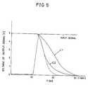
- a variation in the output signal supplied from the output buffer 1 as a function of timeis illustrated by a broken line shown in FIG.5. It can be seen from FIG.5 that the output signal decreases to ground level rapidly. This rapid decrease of the output signal causes a ringing noise.
- FIG.3illustrates a configuration of a conventional low-noise type CMOS output buffer 8 equipped with a ringing noise reduction circuit.
- An input signal Vinis applied to input inverters 9 and 10.
- the input inverter 9is made up of a PMOS transistor 11, and NMOS transistors 12 through 15.
- the gates of the NMOS transistor 13 through 15 connected in seriesare connected to a high-potential power source V DD .
- the source of the NMOS transistor 15is connected to a low-potential power source V SS .
- the input inverter 10is made up of PMOS transistors 16, and 18 through 20, and an NMOS transistor 17.
- the gates of the PMOS transistors 18 through 20 connected in seriesare connected to the low-potential power source V SS .
- the source of the NMOS transistor 17is connected to the low-potential power source V SS .
- the source of the PMOS transistor 18is connected to the high-potential power source V DD .
- the output signal of the input inverter 9is supplied to the gate of a PMOS transistor 22, which is a part of an output inverter 21.
- the output signal of the input inverter 10is supplied to the gate of an NMOS transistor 23, which is another part of the output inverter 21.
- the potential of the source of the NMOS transistor 12is pulled up to a potential V SS′ due to the presence of the NMOS transistors 13 through 15 (V SS′ >V SS ).
- the potential of the drain of the PMOS transistor 16is pulled down to a potential V DD′ due to the presence of the PMOS transistors 18 through 20 (V DD >V DD′ ). Therefore, when the input signal Vin is changed from "L (low level)" to "H” (high level)", the NMOS transistor 12 is not turned ON until the NMOS transistor 12 is supplied with a threshold voltage higher than a normal threshold voltage obtained in case where the CMOS inverter 9 consists of the PMOS and NMOS transistors 11 and 12.
- the threshold voltage of the NMOS transistor 12is set so as to be shifted toward the V DD level. Thereafter, when the input signal Vin exceeds the threshold voltage of the NMOS transistor 12 which is higher than the normal threshold voltage, the NMOS transistor 12 is turned ON and the PMOS transistor 11 is turned OFF. Then the gate of the PMOS transistor 22 becomes equal to the potential V SS′ , and thus the PMOS transistor 22 is turned ON. As a result, an output signal Vout becomes equal to the potential V DD .
- the PMOS transistor 16is not turned ON until the PMOS transistor 16 is supplied with a threshold voltage lower than a normal threshold voltage obtained in case where the CMOS inverter 10 consists of the PMOS and NMOS transistors 16 and 17. Then when the input signal Vin becomes equal to the threshold voltage of the PMOS transistor 16 which is lower than the normal threshold voltage, the PMOS transistor 16 is turned ON and the NMOS transistor 17 is turned OFF. Therefore, the gate of the NMOS transistor 23 becomes equal to the potential V DD′ . As a result, the output signal Vout becomes the potential V SS .
- FIG.3reduces a time during which both the PMOS and NMOS transistors 22 and 23 are ON, and thereby reduces a through current passing therethrough.
- the waveform of the output signal Vout at the output inverter 21is illustrated as a solid line C1 shown in FIG.5. It can be seen from FIG.5 that the output signal available in the output buffer 8 decreases slowly, compared with the output signal available in the output buffer 1 shown in FIG.2.
- the output buffer 8 having the conventional ringing noise reduction circuit shown in FIG.3has the following disadvantages to be overcome.
- the ringing noiseis reduced by slowly decreasing the output signal Vout as indicated by the curve C1.
- the abovecauses an increase of the response time of the output signal Vout, and thus prevents the output buffer 8 from operating with high speeds.
- the output buffer 8does not satisfy high-speed operation and small ringing noise at the same time.
- a more specific object of the present inventionis to provide a semiconductor integrated circuit having a CMOS inverter which can operate at high speeds with extremely reduced ringing noise.
- a semiconductor integrated circuit having a complementary metal oxide semiconductor (CMOS) inverterincludes a CMOS inverter circuit and a noise reduction circuit.
- the CMOS inverterhas input and output terminals and inverts an input signal applied to the input terminal to thereby output an output signal through the output terminal.
- the noise reduction circuitwhich is connected to the CMOS inverter, rapidly passes a current supplied from the CMOS inverter to the low-potential power source until a potential of the output terminal decreases to a predetermined potential in response to an increase in potential of the input signal, and slowly passes the current after the potential of the output terminal reaches the predetermined potential.
- a semiconductor integrated circuitcomprising a CMOS inverter including a first P-channel MOS transistor having a drain, source and gate, and a first N-channel MOS transistor having a drain, source and gate.
- the source of the first P-channel MOS transistoris connected to a high-potential power source, said drains forming an output of the circuit.
- the gates of the first P-channel and N-channel MOS transistorsare mutually connected and supplied with an input signal.
- the circuitalso includes a second N-channel MOS transistor having a drain, source and gate. The drain of the second N-channel MOS transistor is connected to the source of the first N-channel MOS transistor.
- the source of the second N-channel MOS transistoris connected to a low-potential power source.
- the gate of the second N-channel MOS transistoris connected to the gates of the first P-channel and N-channel MOS transistors.
- the circuitincludes a third N-channel MOS transistor having a drain, source and gate. The drain of the third N-channel MOS transistor is connected to the source of the first N-channel MOS transistor.
- the source of the third N-channel MOS transistoris connected to the low-potential power source.
- the gate of the third N-channel MOS transistoris connected to the output of the circuit.
- CMOS buffer 31which includes a CMOS inverter equipped with a ringing noise reduction circuit.
- the CMOS buffer 31functions as a CMOS output buffer, and includes a PMOS transistor Q1 and NMOS transistors Q2, Q3 and Q4.
- the combination of the PMOS and NMOS transistors Q1 and Q2forms an inverter 32.
- the source of the PMOS transistor Q1is connected to the high-potential power source V DD .
- the drains of the PMOS and NMOS transistors Q1 and Q2are mutually connected.
- the combination of the NMOS transistors Q3 and Q4is served as a ringing noise reduction circuit.
- the source of the NMOS transistor Q2is connected to the drains of the NMOS transistors Q3 and Q4.
- the gates of the PMOS transistor Q1 and the NMOS transistors Q2 and Q3are mutually connected, and provided with the input signal Vin through an input terminal IN.
- the gate of the NMOS transistor Q4is connected to the drains of the PMOS and NMOS transistors Q1 and Q2, which are also connected to an output terminal OUT.
- the sources of the NMOS transistors Q3 and Q4are connected to the low-potential power source V SS .
- a capacitor Cindicates a capacitance formed by elements coupled to the output terminal OUT, such as a transistor and a line.
- the NMOS transistors Q2 and Q3go toward the ON state. At this time, a current I from the high-potential power source V DD through the NMOS transistor Q2 passes through the NMOS transistors Q3 and Q4. Then the output signal Vout is changed to "L” level.
- the NMOS transistors Q2 and Q3are maintained in the ON state so long as the input signal Vin is at "H” level. The current I intends to pass through the NMOS transistors Q2 through Q4 until the output signal Vout becomes equal to ground level.
- the NMOS transistor Q4is turned OFF, when the output signal Vout decreases and then reaches the logical threshold level of the NMOS transistor Q4. Therefore, when the output signal Vout is lower than the logical threshold level of the NMOS transistor Q4, the current I from the NMOS transistor Q2 passes through only the NMOS transistor Q3. As a result, the output signal Vout slowly decreases toward ground level after reaching the logical threshold level of the NMOS transistor Q4. In other words, the waveform of the output signal Vout becomes dull.
- the NMOS transistor Q2has the same size as the NMOS transistor 6 or 23, the ON resistance of the N-channel circuit portion consisting of the NMOS transistors Q2 to Q4 is larger than that obtained in case where the N-channel circuit portion consists of only the NMOS transistor Q2.
- the logic threshold level of the CMOS buffer 31is larger than that for the conventional circuit 7 or 21.
- the NMOS transistor Q2is formed by a transistor having the size larger than a transistor used for forming the NMOS transistor 6 or 23.
- the NMOS transistors Q2 and Q4are formed by large-size NMOS transistors (having a large value of the mutual conductance), and the NMOS transistor Q3 is formed by a small-size NMOS transistor (having a small value of the mutual conductance).
- the output signal Voutit is possible to rapidly decrease the output signal Vout to a low potential which is close to and higher than the logical threshold voltage of the NMOS transistor Q4 (approximately 0.65 volts, for example) and thereafter decrease the output signal Vout slowly.
- an ideal waveform of the output signal Voutis available.
- the waveform of the output signal Voutis indicated by a solid line C2 shown in FIG.5. It can be seen from FIG.5 that the waveform of the output signal Vout indicated by the curve C2 satisfies high-speed operation and reduction of a ringing noise at the same time.
- FIG.6is a variation of the CMOS buffer 31.
- An essential feature of this variationis that the NMOS transistor Q4 is made up of two NMOS transistors Q4-1 and Q4-2 connected in parallel. The variation contributes to speeding up the operation of the CMOS buffer 31.
- FIG.7is another variation of the CMOS buffer 31.
- An essential feature of this variationis that the NMOS transistor Q3 is made up of two NMOS transistors Q3-1 and Q3-2 connected in series.
- the variation of FIG.7also contributes to speeding up the circuit operation.
- a ringing noisealso occurs when the input signal Vin decreases from "H” level to "L” level.
- a ringing noisemay not cause a serious problem such as level inversion.
Landscapes
- Physics & Mathematics (AREA)
- Engineering & Computer Science (AREA)
- Computer Hardware Design (AREA)
- Computing Systems (AREA)
- General Engineering & Computer Science (AREA)
- Mathematical Physics (AREA)
- Logic Circuits (AREA)
- Electronic Switches (AREA)
Description
- The present invention generally relates to a semiconductor integrated circuit having a CMOS (complementary metal oxide semiconductor) inverter, and particularly to the suppression of a ringing noise which causes a malfunction of a semiconductor integrated circuit having a CMOS inverter.
- In Patent Abstracts of Japan, vol. 11, no. 154 (E-508) [2601], 19th May 1987 and JP-A-61 292 412 an output circuit is enclosed to prevent undershoot from being generated by lowering an output level voltage rapidly until a prescribed low level voltage and lowering comparatively slowly until the final power voltage level after that so as to decrease a period until the output reaches the specified voltage.
- Currently, there is a trend on increase in the integration level and operational speed of a CMOS transistor circuit. Additionally, a high-speed or high driveability CMOS buffer becomes available. Such a CMOS buffer is frequently used to form an output buffer. As is well known, a ringing noise is a serious problem which frequently occurs in a high-speed or high-driveability CMOS output buffer. Particularly, a ringing noise causes a level inversion when an output signal of a circuit having a CMOS inverter falls.
- Referring to FIG.1, a ringing noise is interposed on an output waveform (b) of a CMOS inverter when an input signal (a) is applied thereto. As is illustrated, the output waveform alternately changes due to the presence of the ringing noise. Generally, the low threshold potential of a CMOS inverter is set equal to approximately 1.5 volts, when a TTL interface is used. Alternatively, the low threshold potential is set equal to approximately 2.5 volts, when a high-potential power source voltage VDD is set equal to 5 volts and a low-potential power source voltage VSS is set equal to 0 volt. Therefore, when the output signal falls, the level of the output signal may be alternately inverted. Also, the potential (c) of a ground terminal (a VSS terminal) of the CMOS buffer changes depending on the change of the output waveform. If a ringing noise is introduced into a bus, for example, it may affect an internal circuit formed in an LSI circuit and causes a malfunction thereof. The reason why ringing frequently occurs in a CMOS circuit is as follows. First, the output waveform changes in a full swing of the power source voltage, between 5 volts to 0 volt, for example. Secondly, a current passes through the CMOS inverter at a dash, and additionally there is no branch path through which the current passes. Particularly, the occurrence of ringing noises described above is a serious problem in aiming to increase the operational speed of MOS transistors.
- FIG.2 illustrates a conventional CMOS output buffer provided with no measurement to count a ringing noise. An
output buffer 1 consists of twocascaded CMOS inverters 4 and 7. TheCMOS inverter 4 is made up of a P-channel MOS transistor (hereinafter simply referred to as a PMOS transistor) 2 and an N-channel MOS transistor (hereinafter simply referred to as an NMOS transistor) 3. Similarly, the CMOS inverter 7 is made up of aPMOS transistor 5 and anNMOS transistor 6. A variation in the output signal supplied from theoutput buffer 1 as a function of time is illustrated by a broken line shown in FIG.5. It can be seen from FIG.5 that the output signal decreases to ground level rapidly. This rapid decrease of the output signal causes a ringing noise. - FIG.3 illustrates a configuration of a conventional low-noise type CMOS output buffer 8 equipped with a ringing noise reduction circuit. An input signal Vin is applied to
input inverters input inverter 9 is made up of aPMOS transistor 11, andNMOS transistors 12 through 15. The gates of theNMOS transistor 13 through 15 connected in series are connected to a high-potential power source VDD. The source of theNMOS transistor 15 is connected to a low-potential power source VSS. Theinput inverter 10 is made up ofPMOS transistors NMOS transistor 17. The gates of thePMOS transistors 18 through 20 connected in series are connected to the low-potential power source VSS. The source of theNMOS transistor 17 is connected to the low-potential power source VSS. The source of thePMOS transistor 18 is connected to the high-potential power source VDD. The output signal of theinput inverter 9 is supplied to the gate of aPMOS transistor 22, which is a part of anoutput inverter 21. The output signal of theinput inverter 10 is supplied to the gate of an NMOS transistor 23, which is another part of theoutput inverter 21. - The potential of the source of the
NMOS transistor 12 is pulled up to a potential VSS′ due to the presence of theNMOS transistors 13 through 15 (VSS′>VSS). The potential of the drain of thePMOS transistor 16 is pulled down to a potential VDD′ due to the presence of thePMOS transistors 18 through 20 (VDD>VDD′). Therefore, when the input signal Vin is changed from "L (low level)" to "H" (high level)", theNMOS transistor 12 is not turned ON until theNMOS transistor 12 is supplied with a threshold voltage higher than a normal threshold voltage obtained in case where theCMOS inverter 9 consists of the PMOS andNMOS transistors NMOS transistor 12 is set so as to be shifted toward the VDD level. Thereafter, when the input signal Vin exceeds the threshold voltage of theNMOS transistor 12 which is higher than the normal threshold voltage, theNMOS transistor 12 is turned ON and thePMOS transistor 11 is turned OFF. Then the gate of thePMOS transistor 22 becomes equal to the potential VSS′, and thus thePMOS transistor 22 is turned ON. As a result, an output signal Vout becomes equal to the potential VDD. - On the other hand, when the input signal Vin is changed from "H" to "L", the
PMOS transistor 16 is not turned ON until thePMOS transistor 16 is supplied with a threshold voltage lower than a normal threshold voltage obtained in case where theCMOS inverter 10 consists of the PMOS andNMOS transistors PMOS transistor 16 which is lower than the normal threshold voltage, thePMOS transistor 16 is turned ON and theNMOS transistor 17 is turned OFF. Therefore, the gate of the NMOS transistor 23 becomes equal to the potential VDD′. As a result, the output signal Vout becomes the potential VSS. In this manner, the improvement of FIG.3 reduces a time during which both the PMOS andNMOS transistors 22 and 23 are ON, and thereby reduces a through current passing therethrough. The waveform of the output signal Vout at theoutput inverter 21 is illustrated as a solid line C1 shown in FIG.5. It can be seen from FIG.5 that the output signal available in the output buffer 8 decreases slowly, compared with the output signal available in theoutput buffer 1 shown in FIG.2. - However, the output buffer 8 having the conventional ringing noise reduction circuit shown in FIG.3 has the following disadvantages to be overcome. As described above, the ringing noise is reduced by slowly decreasing the output signal Vout as indicated by the curve C1. However, the above causes an increase of the response time of the output signal Vout, and thus prevents the output buffer 8 from operating with high speeds. In other words, the output buffer 8 does not satisfy high-speed operation and small ringing noise at the same time.
- It is therefore a general object of the present invention to provide an improved semiconductor integrated circuit having a CMOS inverter in which the above-mentioned disadvantages of the conventional circuit are eliminated.
- A more specific object of the present invention is to provide a semiconductor integrated circuit having a CMOS inverter which can operate at high speeds with extremely reduced ringing noise.
- The above objects of the present invention can be achieved by a semiconductor integrated circuit having a complementary metal oxide semiconductor (CMOS) inverter includes a CMOS inverter circuit and a noise reduction circuit. The CMOS inverter has input and output terminals and inverts an input signal applied to the input terminal to thereby output an output signal through the output terminal. The noise reduction circuit, which is connected to the CMOS inverter, rapidly passes a current supplied from the CMOS inverter to the low-potential power source until a potential of the output terminal decreases to a predetermined potential in response to an increase in potential of the input signal, and slowly passes the current after the potential of the output terminal reaches the predetermined potential.
- The above-mentioned objects of the present invention can also be achieved by a semiconductor integrated circuit comprising a CMOS inverter including a first P-channel MOS transistor having a drain, source and gate, and a first N-channel MOS transistor having a drain, source and gate. The source of the first P-channel MOS transistor is connected to a high-potential power source, said drains forming an output of the circuit. The gates of the first P-channel and N-channel MOS transistors are mutually connected and supplied with an input signal. The circuit also includes a second N-channel MOS transistor having a drain, source and gate. The drain of the second N-channel MOS transistor is connected to the source of the first N-channel MOS transistor. The source of the second N-channel MOS transistor is connected to a low-potential power source. The gate of the second N-channel MOS transistor is connected to the gates of the first P-channel and N-channel MOS transistors. Further, the circuit includes a third N-channel MOS transistor having a drain, source and gate. The drain of the third N-channel MOS transistor is connected to the source of the first N-channel MOS transistor. The source of the third N-channel MOS transistor is connected to the low-potential power source. The gate of the third N-channel MOS transistor is connected to the output of the circuit.
- Other objects, features and advantages of the present invention will become apparent from the following detailed description when read in conjunction with the accompanying drawings.
- FIG.1 is a waveform diagram illustrating a ringing noise which occurs in a CMOS buffer;
- FIG.2 is a circuit diagram of a conventional CMOS buffer which is provided with no measurement to count a ringing noise;
- FIG.3 is a circuit of a conventional CMOS buffer equipped with a ringing noise reduction circuit;
- FIG.4 is a circuit diagram of a preferred embodiment of the present invention;
- FIG.5 is a waveform diagram illustrating the time-variation of output waveforms observed in the conventional circuits of FIGS.2 and 3 and the preferred embodiment shown in FIG.4;
- FIG.6 is a circuit diagram of a variation of the circuit shown in FIG.4; and
- FIG.7 is a circuit diagram of another variation of the circuit shown in FIG.4.
- A description is given of a preferred embodiment with reference to FIG.4. Referring to FIG.4, there is illustrated a
CMOS buffer 31 which includes a CMOS inverter equipped with a ringing noise reduction circuit. TheCMOS buffer 31 functions as a CMOS output buffer, and includes a PMOS transistor Q1 and NMOS transistors Q2, Q3 and Q4. The combination of the PMOS and NMOS transistors Q1 and Q2 forms aninverter 32. The source of the PMOS transistor Q1 is connected to the high-potential power source VDD. The drains of the PMOS and NMOS transistors Q1 and Q2 are mutually connected. The combination of the NMOS transistors Q3 and Q4 is served as a ringing noise reduction circuit. The source of the NMOS transistor Q2 is connected to the drains of the NMOS transistors Q3 and Q4. The gates of the PMOS transistor Q1 and the NMOS transistors Q2 and Q3 are mutually connected, and provided with the input signal Vin through an input terminal IN. The gate of the NMOS transistor Q4 is connected to the drains of the PMOS and NMOS transistors Q1 and Q2, which are also connected to an output terminal OUT. The sources of the NMOS transistors Q3 and Q4 are connected to the low-potential power source VSS. A capacitor C indicates a capacitance formed by elements coupled to the output terminal OUT, such as a transistor and a line. - In operation, when the input signal Vin is switched from "L" level to "H" level, the NMOS transistors Q2 and Q3 go toward the ON state. At this time, a current I from the high-potential power source VDD through the NMOS transistor Q2 passes through the NMOS transistors Q3 and Q4. Then the output signal Vout is changed to "L" level. The NMOS transistors Q2 and Q3 are maintained in the ON state so long as the input signal Vin is at "H" level. The current I intends to pass through the NMOS transistors Q2 through Q4 until the output signal Vout becomes equal to ground level. However, the NMOS transistor Q4 is turned OFF, when the output signal Vout decreases and then reaches the logical threshold level of the NMOS transistor Q4. Therefore, when the output signal Vout is lower than the logical threshold level of the NMOS transistor Q4, the current I from the NMOS transistor Q2 passes through only the NMOS transistor Q3. As a result, the output signal Vout slowly decreases toward ground level after reaching the logical threshold level of the NMOS transistor Q4. In other words, the waveform of the output signal Vout becomes dull.
- It is noted that if the NMOS transistor Q2 has the same size as the
NMOS transistor 6 or 23, the ON resistance of the N-channel circuit portion consisting of the NMOS transistors Q2 to Q4 is larger than that obtained in case where the N-channel circuit portion consists of only the NMOS transistor Q2. In this case, the logic threshold level of theCMOS buffer 31 is larger than that for theconventional circuit 7 or 21. In order to obtain the logic threshold level of theCMOS buffer 31 almost identical to that for the conventional inverter, the NMOS transistor Q2 is formed by a transistor having the size larger than a transistor used for forming theNMOS transistor 6 or 23. - Additionally, it is possible to adjust the decreasing speed of the output signal Vout by changing the size of the NMOS transistors Q2, Q3 and Q4. For example, the NMOS transistors Q2 and Q4 are formed by large-size NMOS transistors (having a large value of the mutual conductance), and the NMOS transistor Q3 is formed by a small-size NMOS transistor (having a small value of the mutual conductance). Thereby, it is possible to rapidly decrease the output signal Vout to a low potential which is close to and higher than the logical threshold voltage of the NMOS transistor Q4 (approximately 0.65 volts, for example) and thereafter decrease the output signal Vout slowly. As a result, an ideal waveform of the output signal Vout is available.
- The waveform of the output signal Vout is indicated by a solid line C2 shown in FIG.5. It can be seen from FIG.5 that the waveform of the output signal Vout indicated by the curve C2 satisfies high-speed operation and reduction of a ringing noise at the same time.
- FIG.6 is a variation of the
CMOS buffer 31. An essential feature of this variation is that the NMOS transistor Q4 is made up of two NMOS transistors Q4-1 and Q4-2 connected in parallel. The variation contributes to speeding up the operation of theCMOS buffer 31. - FIG.7 is another variation of the
CMOS buffer 31. An essential feature of this variation is that the NMOS transistor Q3 is made up of two NMOS transistors Q3-1 and Q3-2 connected in series. The variation of FIG.7 also contributes to speeding up the circuit operation. In the variations of FIGS.6 and 7, it is also possible to use three or more NMOS transistors to form the NMOS transistor Q3 and/or Q4. - A ringing noise also occurs when the input signal Vin decreases from "H" level to "L" level. However, such a ringing noise may not cause a serious problem such as level inversion.
Claims (8)
- A semiconductor integrated circuit comprising
a CMOS inverter (32) including a first P-channel MOS transistor (Q1) having a drain, source and gate, and a first N-channel MOS transistor (Q2) having a drain, source and gate, the source of said first P-channel MOS transistor being connected to a high-potential power source (VDD), the said drains forming an output of said circuit, the gates of said first P-channel and N-channel MOS transistors being mutually connected and supplied with an input signal,
a second N-channel MOS transistor (Q3) having a drain, source and gate, the drain of said second N-channel MOS transistor (Q3) being connected to the source of said first N-channel MOS transistor, the source of said second N-channel MOS transistor (Q3) being connected to a low-potential power source (VSSS), and
a third N-channel MOS transistor (Q4) having a drain, source and gate, the source of said third N-channel MOS transistor (Q4) being connected to said low-potential power source (VSS),characterized in that
the gate of said second N-channel MOS transistor (Q3) is connected to the gates of said first P-channel and N-channel MOS transistors,
the drain of said third N-channel MOS transistor (Q4) is connected to the source of said first N-channel MOS transistor (Q2), and
the gate of said third N-channel MOS transistor (Q4) is connected to said output of the circuit. - A semiconductor integrated circuit as claimed in claim 1, characterized in that said CMOS inverter means (32) has high and low threshold potentials defining logical values.
- A semiconductor integrated circuit as claimed in claim 1 or 2, characterized in that said third N-channel MOS transistor (Q4) has a mutual conductance higher than that of said second N-channel MOS transistor (Q3).
- A semiconductor integrated circuit as claimed in claim 2 or 3, characterized in that said CMOS inverter means (32) including said first P-channel MOS transistor (Q1) and said first N-channel MOS transistor (Q2), and said first N-channel MOS transistor (Q2) has a mutual conductance higher than that of said second N-channel MOS transistor (Q3).
- A semiconductor integrated circuit as claimed in any of claims 2 to 4, characterized in that said second N-channel MOS transistor (Q3) includes a plurality of MOS transistors (Q3-1, Q3-2) connected in series.
- A semiconductor integrated circuit as claimed in any of claims 2 to 5, characterized in that said third N-channel MOS transistor (Q4) includes a plurality of MOS transistors (Q4-1, Q4-2) connected in parallel.
- A semiconductor integrated circuit as claimed in any of claims 1 to 6, characterized in that said circuit forms an output buffer (31).
- A semiconductor integrated circuit as claimed in any of claims 1 to 7, characterized in that said second and third N-channel MOS transistors (Q3, Q4) form a ringing noise reduction circuit.
Applications Claiming Priority (2)
| Application Number | Priority Date | Filing Date | Title |
|---|---|---|---|
| JP150848/88 | 1988-06-17 | ||
| JP63150848AJP2542678B2 (en) | 1988-06-17 | 1988-06-17 | Semiconductor device |
Publications (2)
| Publication Number | Publication Date |
|---|---|
| EP0346876A1 EP0346876A1 (en) | 1989-12-20 |
| EP0346876B1true EP0346876B1 (en) | 1994-09-14 |
Family
ID=15505701
Family Applications (1)
| Application Number | Title | Priority Date | Filing Date |
|---|---|---|---|
| EP89110814AExpired - LifetimeEP0346876B1 (en) | 1988-06-17 | 1989-06-14 | Semiconductor integrated circuit having a CMOS inverter |
Country Status (5)
| Country | Link |
|---|---|
| US (1) | US5073727A (en) |
| EP (1) | EP0346876B1 (en) |
| JP (1) | JP2542678B2 (en) |
| KR (1) | KR930000972B1 (en) |
| DE (1) | DE68918164T2 (en) |
Families Citing this family (21)
| Publication number | Priority date | Publication date | Assignee | Title |
|---|---|---|---|---|
| JP3194982B2 (en)* | 1991-04-17 | 2001-08-06 | ヤマハ発動機株式会社 | Method of manufacturing engine valve lifter |
| US5319260A (en)* | 1991-07-23 | 1994-06-07 | Standard Microsystems Corporation | Apparatus and method to prevent the disturbance of a quiescent output buffer caused by ground bounce or by power bounce induced by neighboring active output buffers |
| KR940010671B1 (en)* | 1992-07-25 | 1994-10-24 | 금성일렉트론 주식회사 | Cmos 3-state buffer circuit and control method |
| JPH06224734A (en)* | 1992-12-01 | 1994-08-12 | Nec Corp | Input circuit |
| GB9404013D0 (en)* | 1994-03-02 | 1994-04-20 | Inmos Ltd | Current generating unit |
| DE69503205T2 (en)* | 1994-03-25 | 1999-02-11 | Philips Electronics N.V., Eindhoven | CMOS INPUT WITH VCC COMPENSATED DYNAMIC THRESHOLD |
| JP3229164B2 (en)* | 1994-07-28 | 2001-11-12 | インターナショナル・ビジネス・マシーンズ・コーポレーション | Latch circuit |
| US5491429A (en)* | 1994-09-16 | 1996-02-13 | At&T Global Information Solutions Company | Apparatus for reducing current consumption in a CMOS inverter circuit |
| US5514979A (en)* | 1994-11-28 | 1996-05-07 | Unisys Corporation | Methods and apparatus for dynamically reducing ringing of driver output signal |
| FR2730367A1 (en)* | 1995-02-08 | 1996-08-09 | Bull Sa | INPUT COUPLER OUTPUT OF INTEGRATED CIRCUIT |
| JP3618424B2 (en)* | 1995-09-07 | 2005-02-09 | エイ・アイ・エル株式会社 | Low power logic circuit |
| EP1479164A1 (en)* | 2002-02-21 | 2004-11-24 | Koninklijke Philips Electronics N.V. | Integrated circuit having reduced substrate bounce |
| US6870895B2 (en)* | 2002-12-19 | 2005-03-22 | Semiconductor Energy Laboratory Co., Ltd. | Shift register and driving method thereof |
| KR100549872B1 (en)* | 2003-12-10 | 2006-02-06 | 삼성전자주식회사 | Differential Switching Circuits and Digital Analog Converters |
| KR20070012972A (en)* | 2005-07-25 | 2007-01-30 | 삼성전자주식회사 | Display device, driving device and method |
| US8415972B2 (en)* | 2010-11-17 | 2013-04-09 | Advanced Micro Devices, Inc. | Variable-width power gating module |
| US8384421B1 (en) | 2011-04-21 | 2013-02-26 | Applied Micro Circuits Corporation | Digital CMOS circuit with noise cancellation |
| US8837188B1 (en) | 2011-06-23 | 2014-09-16 | Netlogic Microsystems, Inc. | Content addressable memory row having virtual ground and charge sharing |
| US8773880B2 (en) | 2011-06-23 | 2014-07-08 | Netlogic Microsystems, Inc. | Content addressable memory array having virtual ground nodes |
| US20200136595A1 (en)* | 2018-10-29 | 2020-04-30 | Stmicroelectronics International N.V. | Schmitt trigger circuit with independent control over high and low trip points using a split architecture |
| CN118138017B (en)* | 2024-03-21 | 2025-04-11 | 上海芯炽科技集团有限公司 | A low power Schmitt trigger structure |
Family Cites Families (16)
| Publication number | Priority date | Publication date | Assignee | Title |
|---|---|---|---|---|
| US4490627A (en)* | 1982-11-17 | 1984-12-25 | Motorola, Inc. | Schmitt trigger circuit |
| US4687954A (en)* | 1984-03-06 | 1987-08-18 | Kabushiki Kaisha Toshiba | CMOS hysteresis circuit with enable switch or natural transistor |
| JPS61292412A (en)* | 1985-06-20 | 1986-12-23 | Fujitsu Ltd | Output circuit |
| JPH0720060B2 (en)* | 1985-08-14 | 1995-03-06 | 株式会社東芝 | Output circuit device |
| US4638187A (en)* | 1985-10-01 | 1987-01-20 | Vtc Incorporated | CMOS output buffer providing high drive current with minimum output signal distortion |
| US4649295A (en)* | 1986-01-13 | 1987-03-10 | Motorola, Inc. | BIMOS logic gate |
| JPS62220026A (en)* | 1986-03-20 | 1987-09-28 | Toshiba Corp | Output buffer circuit |
| JPS635553A (en)* | 1986-06-25 | 1988-01-11 | Fujitsu Ltd | Buffer circuit |
| US4749882A (en)* | 1986-07-25 | 1988-06-07 | Digital Equipment Corporation | Apparatus and method for applying rapid transient signals to components on a printed circuit board |
| US4731553A (en)* | 1986-09-30 | 1988-03-15 | Texas Instruments Incorporated | CMOS output buffer having improved noise characteristics |
| US4739193A (en)* | 1986-10-30 | 1988-04-19 | Rca Corporation | Drive circuit with limited signal transition rate for RFI reduction |
| JPS63236407A (en)* | 1987-03-25 | 1988-10-03 | Toshiba Corp | semiconductor circuit |
| US4829199A (en)* | 1987-07-13 | 1989-05-09 | Ncr Corporation | Driver circuit providing load and time adaptive current |
| US4818901A (en)* | 1987-07-20 | 1989-04-04 | Harris Corporation | Controlled switching CMOS output buffer |
| US4820942A (en)* | 1988-01-27 | 1989-04-11 | Advanced Micro Devices, Inc. | High-speed, high-drive output buffer circuits with reduced ground bounce |
| US4857770A (en)* | 1988-02-29 | 1989-08-15 | Advanced Micro Devices, Inc. | Output buffer arrangement for reducing chip noise without speed penalty |
- 1988
- 1988-06-17JPJP63150848Apatent/JP2542678B2/ennot_activeExpired - Fee Related
- 1989
- 1989-05-25USUS07/356,920patent/US5073727A/ennot_activeExpired - Lifetime
- 1989-06-14DEDE68918164Tpatent/DE68918164T2/ennot_activeExpired - Fee Related
- 1989-06-14EPEP89110814Apatent/EP0346876B1/ennot_activeExpired - Lifetime
- 1989-06-17KRKR1019890008378Apatent/KR930000972B1/ennot_activeExpired - Fee Related
Non-Patent Citations (1)
| Title |
|---|
| PATENT ABSTRACTS OF JAPAN, vol.11, no.154 (E-508)(2601) 19 May 1987 & JP-A-61292412* |
Also Published As
| Publication number | Publication date |
|---|---|
| KR900001042A (en) | 1990-01-31 |
| JP2542678B2 (en) | 1996-10-09 |
| DE68918164D1 (en) | 1994-10-20 |
| JPH024008A (en) | 1990-01-09 |
| EP0346876A1 (en) | 1989-12-20 |
| US5073727A (en) | 1991-12-17 |
| KR930000972B1 (en) | 1993-02-11 |
| DE68918164T2 (en) | 1995-04-27 |
Similar Documents
| Publication | Publication Date | Title |
|---|---|---|
| EP0346876B1 (en) | Semiconductor integrated circuit having a CMOS inverter | |
| US4779013A (en) | Slew-rate limited output driver having reduced switching noise | |
| US5041741A (en) | Transient immune input buffer | |
| US5017807A (en) | Output buffer having capacitive drive shunt for reduced noise | |
| US4908528A (en) | Input circuit having improved noise immunity | |
| US5043604A (en) | Output buffer circuit having a level conversion function | |
| US4931668A (en) | MIS transistor driven inverter circuit capable of individually controlling rising portion and falling portion of output waveform | |
| US4880998A (en) | Bipolar transistor and CMOS transistor logic circuit having improved discharge capabilities | |
| US5057713A (en) | Bipolar MOS logic circuit and semiconductor integrated circuit | |
| JPH06216759A (en) | Semiconductor integrated circuit device | |
| US5132569A (en) | High speed Bi-COMS input circuit fabricated from a small number of circuit components | |
| JP3021145B2 (en) | Method and apparatus for noise control on a power supply bus | |
| US5541528A (en) | CMOS buffer circuit having increased speed | |
| US6175598B1 (en) | Output noise control scheme for multiple I/O's | |
| JPH06152374A (en) | Output circuit | |
| US5268597A (en) | Output buffer circuit with noise reduction circuit | |
| US6335649B1 (en) | Schmitt trigger circuit | |
| US20230327652A1 (en) | Semiconductor device and input signal controlling method | |
| US5247214A (en) | Bi-cmos out buffer circuit for cmos logic | |
| EP0284936A2 (en) | TTL-compatible cell for CMOS integrated circuits | |
| JP2767909B2 (en) | Output buffer circuit | |
| US5619153A (en) | Fast swing-limited pullup circuit | |
| US6215341B1 (en) | Deceleration circuit | |
| KR920010349B1 (en) | Noise reduction circuit | |
| US5382842A (en) | Composite logic circuit with bipolar transistor-complementary field effect transistor |
Legal Events
| Date | Code | Title | Description |
|---|---|---|---|
| PUAI | Public reference made under article 153(3) epc to a published international application that has entered the european phase | Free format text:ORIGINAL CODE: 0009012 | |
| AK | Designated contracting states | Kind code of ref document:A1 Designated state(s):DE FR GB | |
| 17P | Request for examination filed | Effective date:19900619 | |
| 17Q | First examination report despatched | Effective date:19920430 | |
| GRAA | (expected) grant | Free format text:ORIGINAL CODE: 0009210 | |
| AK | Designated contracting states | Kind code of ref document:B1 Designated state(s):DE FR GB | |
| REF | Corresponds to: | Ref document number:68918164 Country of ref document:DE Date of ref document:19941020 | |
| ET | Fr: translation filed | ||
| PLBE | No opposition filed within time limit | Free format text:ORIGINAL CODE: 0009261 | |
| STAA | Information on the status of an ep patent application or granted ep patent | Free format text:STATUS: NO OPPOSITION FILED WITHIN TIME LIMIT | |
| 26N | No opposition filed | ||
| REG | Reference to a national code | Ref country code:GB Ref legal event code:IF02 | |
| PGFP | Annual fee paid to national office [announced via postgrant information from national office to epo] | Ref country code:GB Payment date:20050608 Year of fee payment:17 Ref country code:FR Payment date:20050608 Year of fee payment:17 | |
| PGFP | Annual fee paid to national office [announced via postgrant information from national office to epo] | Ref country code:DE Payment date:20050609 Year of fee payment:17 | |
| PG25 | Lapsed in a contracting state [announced via postgrant information from national office to epo] | Ref country code:GB Free format text:LAPSE BECAUSE OF NON-PAYMENT OF DUE FEES Effective date:20060614 | |
| PG25 | Lapsed in a contracting state [announced via postgrant information from national office to epo] | Ref country code:DE Free format text:LAPSE BECAUSE OF NON-PAYMENT OF DUE FEES Effective date:20070103 | |
| GBPC | Gb: european patent ceased through non-payment of renewal fee | Effective date:20060614 | |
| REG | Reference to a national code | Ref country code:FR Ref legal event code:ST Effective date:20070228 | |
| PG25 | Lapsed in a contracting state [announced via postgrant information from national office to epo] | Ref country code:FR Free format text:LAPSE BECAUSE OF NON-PAYMENT OF DUE FEES Effective date:20060630 |