EP0342937B1 - Manufacturing a semiconductor wafer having a III-V group semiconductor compound layer on a silicon substrate - Google Patents
Manufacturing a semiconductor wafer having a III-V group semiconductor compound layer on a silicon substrateDownload PDFInfo
- Publication number
- EP0342937B1 EP0342937B1EP89304953AEP89304953AEP0342937B1EP 0342937 B1EP0342937 B1EP 0342937B1EP 89304953 AEP89304953 AEP 89304953AEP 89304953 AEP89304953 AEP 89304953AEP 0342937 B1EP0342937 B1EP 0342937B1
- Authority
- EP
- European Patent Office
- Prior art keywords
- temperature
- layer
- gaas
- amorphous layer
- amorphous
- Prior art date
- Legal status (The legal status is an assumption and is not a legal conclusion. Google has not performed a legal analysis and makes no representation as to the accuracy of the status listed.)
- Expired - Lifetime
Links
Images


Classifications
- H—ELECTRICITY
- H01—ELECTRIC ELEMENTS
- H01L—SEMICONDUCTOR DEVICES NOT COVERED BY CLASS H10
- H01L21/00—Processes or apparatus adapted for the manufacture or treatment of semiconductor or solid state devices or of parts thereof
- H01L21/02—Manufacture or treatment of semiconductor devices or of parts thereof
- H01L21/02104—Forming layers
- H01L21/02365—Forming inorganic semiconducting materials on a substrate
- H01L21/02436—Intermediate layers between substrates and deposited layers
- H01L21/02439—Materials
- H01L21/02455—Group 13/15 materials
- H01L21/02463—Arsenides
- H—ELECTRICITY
- H01—ELECTRIC ELEMENTS
- H01L—SEMICONDUCTOR DEVICES NOT COVERED BY CLASS H10
- H01L21/00—Processes or apparatus adapted for the manufacture or treatment of semiconductor or solid state devices or of parts thereof
- H01L21/02—Manufacture or treatment of semiconductor devices or of parts thereof
- H01L21/04—Manufacture or treatment of semiconductor devices or of parts thereof the devices having potential barriers, e.g. a PN junction, depletion layer or carrier concentration layer
- H01L21/18—Manufacture or treatment of semiconductor devices or of parts thereof the devices having potential barriers, e.g. a PN junction, depletion layer or carrier concentration layer the devices having semiconductor bodies comprising elements of Group IV of the Periodic Table or AIIIBV compounds with or without impurities, e.g. doping materials
- H01L21/20—Deposition of semiconductor materials on a substrate, e.g. epitaxial growth solid phase epitaxy
- H—ELECTRICITY
- H01—ELECTRIC ELEMENTS
- H01L—SEMICONDUCTOR DEVICES NOT COVERED BY CLASS H10
- H01L21/00—Processes or apparatus adapted for the manufacture or treatment of semiconductor or solid state devices or of parts thereof
- H01L21/02—Manufacture or treatment of semiconductor devices or of parts thereof
- H01L21/02104—Forming layers
- H01L21/02365—Forming inorganic semiconducting materials on a substrate
- H01L21/02367—Substrates
- H01L21/0237—Materials
- H01L21/02373—Group 14 semiconducting materials
- H01L21/02381—Silicon, silicon germanium, germanium
- H—ELECTRICITY
- H01—ELECTRIC ELEMENTS
- H01L—SEMICONDUCTOR DEVICES NOT COVERED BY CLASS H10
- H01L21/00—Processes or apparatus adapted for the manufacture or treatment of semiconductor or solid state devices or of parts thereof
- H01L21/02—Manufacture or treatment of semiconductor devices or of parts thereof
- H01L21/02104—Forming layers
- H01L21/02365—Forming inorganic semiconducting materials on a substrate
- H01L21/02436—Intermediate layers between substrates and deposited layers
- H01L21/02494—Structure
- H01L21/02496—Layer structure
- H01L21/02502—Layer structure consisting of two layers
- H—ELECTRICITY
- H01—ELECTRIC ELEMENTS
- H01L—SEMICONDUCTOR DEVICES NOT COVERED BY CLASS H10
- H01L21/00—Processes or apparatus adapted for the manufacture or treatment of semiconductor or solid state devices or of parts thereof
- H01L21/02—Manufacture or treatment of semiconductor devices or of parts thereof
- H01L21/02104—Forming layers
- H01L21/02365—Forming inorganic semiconducting materials on a substrate
- H01L21/02436—Intermediate layers between substrates and deposited layers
- H01L21/02494—Structure
- H01L21/02513—Microstructure
- H—ELECTRICITY
- H01—ELECTRIC ELEMENTS
- H01L—SEMICONDUCTOR DEVICES NOT COVERED BY CLASS H10
- H01L21/00—Processes or apparatus adapted for the manufacture or treatment of semiconductor or solid state devices or of parts thereof
- H01L21/02—Manufacture or treatment of semiconductor devices or of parts thereof
- H01L21/02104—Forming layers
- H01L21/02365—Forming inorganic semiconducting materials on a substrate
- H01L21/02518—Deposited layers
- H01L21/02521—Materials
- H01L21/02538—Group 13/15 materials
- H01L21/02543—Phosphides
- H—ELECTRICITY
- H01—ELECTRIC ELEMENTS
- H01L—SEMICONDUCTOR DEVICES NOT COVERED BY CLASS H10
- H01L21/00—Processes or apparatus adapted for the manufacture or treatment of semiconductor or solid state devices or of parts thereof
- H01L21/02—Manufacture or treatment of semiconductor devices or of parts thereof
- H01L21/02104—Forming layers
- H01L21/02365—Forming inorganic semiconducting materials on a substrate
- H01L21/02518—Deposited layers
- H01L21/02521—Materials
- H01L21/02538—Group 13/15 materials
- H01L21/02546—Arsenides
- H—ELECTRICITY
- H01—ELECTRIC ELEMENTS
- H01L—SEMICONDUCTOR DEVICES NOT COVERED BY CLASS H10
- H01L21/00—Processes or apparatus adapted for the manufacture or treatment of semiconductor or solid state devices or of parts thereof
- H01L21/02—Manufacture or treatment of semiconductor devices or of parts thereof
- H01L21/02104—Forming layers
- H01L21/02365—Forming inorganic semiconducting materials on a substrate
- H01L21/02612—Formation types
- H01L21/02617—Deposition types
- H01L21/0262—Reduction or decomposition of gaseous compounds, e.g. CVD
- Y—GENERAL TAGGING OF NEW TECHNOLOGICAL DEVELOPMENTS; GENERAL TAGGING OF CROSS-SECTIONAL TECHNOLOGIES SPANNING OVER SEVERAL SECTIONS OF THE IPC; TECHNICAL SUBJECTS COVERED BY FORMER USPC CROSS-REFERENCE ART COLLECTIONS [XRACs] AND DIGESTS
- Y10—TECHNICAL SUBJECTS COVERED BY FORMER USPC
- Y10S—TECHNICAL SUBJECTS COVERED BY FORMER USPC CROSS-REFERENCE ART COLLECTIONS [XRACs] AND DIGESTS
- Y10S148/00—Metal treatment
- Y10S148/025—Deposition multi-step
- Y—GENERAL TAGGING OF NEW TECHNOLOGICAL DEVELOPMENTS; GENERAL TAGGING OF CROSS-SECTIONAL TECHNOLOGIES SPANNING OVER SEVERAL SECTIONS OF THE IPC; TECHNICAL SUBJECTS COVERED BY FORMER USPC CROSS-REFERENCE ART COLLECTIONS [XRACs] AND DIGESTS
- Y10—TECHNICAL SUBJECTS COVERED BY FORMER USPC
- Y10S—TECHNICAL SUBJECTS COVERED BY FORMER USPC CROSS-REFERENCE ART COLLECTIONS [XRACs] AND DIGESTS
- Y10S148/00—Metal treatment
- Y10S148/072—Heterojunctions
- Y—GENERAL TAGGING OF NEW TECHNOLOGICAL DEVELOPMENTS; GENERAL TAGGING OF CROSS-SECTIONAL TECHNOLOGIES SPANNING OVER SEVERAL SECTIONS OF THE IPC; TECHNICAL SUBJECTS COVERED BY FORMER USPC CROSS-REFERENCE ART COLLECTIONS [XRACs] AND DIGESTS
- Y10—TECHNICAL SUBJECTS COVERED BY FORMER USPC
- Y10S—TECHNICAL SUBJECTS COVERED BY FORMER USPC CROSS-REFERENCE ART COLLECTIONS [XRACs] AND DIGESTS
- Y10S148/00—Metal treatment
- Y10S148/097—Lattice strain and defects
- Y—GENERAL TAGGING OF NEW TECHNOLOGICAL DEVELOPMENTS; GENERAL TAGGING OF CROSS-SECTIONAL TECHNOLOGIES SPANNING OVER SEVERAL SECTIONS OF THE IPC; TECHNICAL SUBJECTS COVERED BY FORMER USPC CROSS-REFERENCE ART COLLECTIONS [XRACs] AND DIGESTS
- Y10—TECHNICAL SUBJECTS COVERED BY FORMER USPC
- Y10S—TECHNICAL SUBJECTS COVERED BY FORMER USPC CROSS-REFERENCE ART COLLECTIONS [XRACs] AND DIGESTS
- Y10S148/00—Metal treatment
- Y10S148/154—Solid phase epitaxy
- Y—GENERAL TAGGING OF NEW TECHNOLOGICAL DEVELOPMENTS; GENERAL TAGGING OF CROSS-SECTIONAL TECHNOLOGIES SPANNING OVER SEVERAL SECTIONS OF THE IPC; TECHNICAL SUBJECTS COVERED BY FORMER USPC CROSS-REFERENCE ART COLLECTIONS [XRACs] AND DIGESTS
- Y10—TECHNICAL SUBJECTS COVERED BY FORMER USPC
- Y10S—TECHNICAL SUBJECTS COVERED BY FORMER USPC CROSS-REFERENCE ART COLLECTIONS [XRACs] AND DIGESTS
- Y10S438/00—Semiconductor device manufacturing: process
- Y10S438/933—Germanium or silicon or Ge-Si on III-V
- Y—GENERAL TAGGING OF NEW TECHNOLOGICAL DEVELOPMENTS; GENERAL TAGGING OF CROSS-SECTIONAL TECHNOLOGIES SPANNING OVER SEVERAL SECTIONS OF THE IPC; TECHNICAL SUBJECTS COVERED BY FORMER USPC CROSS-REFERENCE ART COLLECTIONS [XRACs] AND DIGESTS
- Y10—TECHNICAL SUBJECTS COVERED BY FORMER USPC
- Y10S—TECHNICAL SUBJECTS COVERED BY FORMER USPC CROSS-REFERENCE ART COLLECTIONS [XRACs] AND DIGESTS
- Y10S438/00—Semiconductor device manufacturing: process
- Y10S438/938—Lattice strain control or utilization
Definitions
- the present inventionrelates to manufacturing a semiconductor wafer having a III-V group semiconductor compound layer on a silicon substrate, and, more particularly, to a method of growing a III-V group compound semiconductor crystalline thin film of, for example, GaAs or the like on a silicon substrate.
- Heteroepitaxial growth of a III-V group compound semiconductor crystalline thin film of, for example, GaAs or the like, on a silicon (Si) substratecan be carried out by a Metalorganic Chemical Vapour Deposition (MOCVD) process or a Molecular Beam Epitaxy (MBE) process.
- MOCVDMetalorganic Chemical Vapour Deposition
- MBEMolecular Beam Epitaxy
- the crystal lattice constants of Si and GaAsare 0.543nm and 0.565nm (5.43 ⁇ and 5.65 ⁇ ) respectively, and the thermal expansion coefficients thereof are 2.6 x 10 ⁇ 6/°C and 5.9 x 10 ⁇ 6/°C, respectively.
- the crystal lattice constant and, in particular, the thermal expansion coefficient of Sidiffer from those of GaAs, when a GaAs layer is formed on a Si substrate by the MOCVD process, the GaAs is formed thereon in a polycrystalline state.
- crystalline GaAsis grown to a thickness of 3 to 5 ⁇ m at a temperature of 700 to 750°C, thereby obtaining a GaAs single crystalline thin film by a two-step process in which the mismatching of the respective lattice constants of Si and GaAs is relaxed, i.e. the problem is overcome, by the occurrence of defects at the interface between the Si and GaAs.
- a tension stress stronger than 1 x 10⁸ Pa (109 dyn/cm2) or moreis generated, and therefore, when the substrate is subjected to a heat treatment after the GaAs growth, lattice defects such as dislocation and the like are formed therein which result in cracks 10 (Fig. 1), and thus, in practice, the formation of a GaAs layer on an Si substrate is not considered viable.
- the reference numerals 1, 2 and 3denote a silicon (Si) substrate, an amorphous GaAs layer and a GaAs crystalline layer, respectively.
- a method of manufacturing a semiconductor wafercomprising the steps of forming a first amorphous layer of a III-V group semiconductor compound on a silicon substrate, and forming a first monocrystalline layer of said semiconductor compound on the said amorphous layer; characterised by the further steps of forming a second amorphous layer of the said semiconductor compound on the first monocrystalline layer, and bringing about solid phase epitaxial growth, from the said first monocrystalline layer, through the said second amorphous layer so as to transform that second amorphous layer into a second monocrystalline layer of the said semiconductor compound.
- the said semiconductor materialconsists of the said III-V group semiconductor compound.
- formation of said first amorphous layeris carried out at a first temperature
- formation of said first monocrystalline layeris carried out at a second temperature higher than said first temperature
- formation of said second amorphous layeris carried out at a third temperature lower than said second temperature
- transformation of said second amorphous layer into said second monocrystalline layeris carried out at a fourth temperature between said second temperature and said third temperature.
- said second amorphous layerhas a thickness greater than that of said first monocrystalline layer.
- the first step of a method embodying the present inventioncomprises forming a first amorphous GaAs layer 2 having a thickness of 10nm to 20nm (100 ⁇ to 200 ⁇ ) on a silicon substrate 1 having a diameter of approximately 5cm (2 inches), at a temperature of 450°C, by a usual MOCVD process.
- a second amorphous GaAs layer 4 having a thickness of about 3 to 5 ⁇ mis formed on the GaAs crystal layer 3, at a temperature of 400° - 450°C.
- trimethyl-gallium(TMG: (CH3)3Ga) was used as a source gas of gallium (Ga), at a TMG supply rate of 15 cm3/min (15cc/min).
- arsine(AsH3) was used as a source gas of arsenic (As), at a AsH3 supply rate of 450 cm3/min (450cc/min), and H2 gas was used at a supply rate of 10 l/min, as a carrier gas of the source gases, TMG and AsH3.
- the above-mentioned heat treatmentwas carried out by using an inductive heating method.
- the obtained substrateis annealed at a temperature lower than the temperature of 700 to 750°C at which the GaAs crystal layer 3 was formed, for example at about 500 to about 650°C, using an atmosphere containing AsH3 supplied at a rate of 100 cm3/min (100cc/min) and H2 supplied at a rate of 1 l/min, whereby solid phase epitaxial growth is carried out from the GaAs crystal layer 3 and the amorphous GaAs layer 4 gradually changes to a GaAs crystal layer 4a, from the lower portion thereof.
- Warping of a thus-obtained GaAs crystal - Si substrate (wafer)can be reduced from the conventional 60 ⁇ m to about 20 ⁇ m.
- FIG. 3illustrates schematically a main reacting portion of MOCVD apparatus which is suitable for use in carrying out the above-described method.
- a silicon substrate (wafer) 1is provided on a carbon susceptor 6 provided in an MOCVD reacting vessel 5 which is inductively heated using a heating coil 7.
- the reacting gases TMG and AsH3, or the carrier gas H2is supplied to the vessel to form a GaAs layer (not shown).
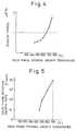
- the tension stress in a GaAs layer obtained at a temperature below 650°Cis 1 x 10⁸ Pa (1 x 10⁹ dyn/cm2) or less, as shown in Fig. 4, which illustrates the relationship between the tension stress in the GaAs layer and the solid phase epitaxial growth temperature.
- Figure 5shows the relationship between the solid phase epitaxial growth rate and the solid phase epitaxial growth temperature.
- the solid phase epitaxial growth rateis significantly less when the temperature is less than 500°C than when the temperature is in the preferred range from 500 to 650°C.
- MOCVDMetal Organic Chemical Vapor Deposition
- MBEMolecular Beam Epitaxy
- GaP, GaAs x P 1-x , In x Ga 1-x As, Ga 1-x As x P 1-x or InPcan be used as the III-V group semiconductor compound instead of GaAs.
- the warping and the stress of a wafer obtained by heteroepitaxial growthfor example a GaAs growth on a Si substrate
- the warping and the stress of a wafer obtained by heteroepitaxial growthcan be decreased in comparison with a wafer produced by a previously-considered method, thereby enabling, for example, a shift of the threshold voltage (Vth) etc. of the FET's which are fabricated on GaAs to be prevented.
- Vththreshold voltage
Landscapes
- Engineering & Computer Science (AREA)
- Physics & Mathematics (AREA)
- Condensed Matter Physics & Semiconductors (AREA)
- General Physics & Mathematics (AREA)
- Manufacturing & Machinery (AREA)
- Computer Hardware Design (AREA)
- Microelectronics & Electronic Packaging (AREA)
- Power Engineering (AREA)
- Chemical & Material Sciences (AREA)
- Crystallography & Structural Chemistry (AREA)
- Materials Engineering (AREA)
- Recrystallisation Techniques (AREA)
Description
- The present invention relates to manufacturing a semiconductor wafer having a III-V group semiconductor compound layer on a silicon substrate, and, more particularly, to a method of growing a III-V group compound semiconductor crystalline thin film of, for example, GaAs or the like on a silicon substrate.
- Heteroepitaxial growth of a III-V group compound semiconductor crystalline thin film of, for example, GaAs or the like, on a silicon (Si) substrate can be carried out by a Metalorganic Chemical Vapour Deposition (MOCVD) process or a Molecular Beam Epitaxy (MBE) process.
- The crystal lattice constants of Si and GaAs are 0.543nm and 0.565nm (5.43 Å and 5.65 Å) respectively, and the thermal expansion coefficients thereof are 2.6 x 10⁻⁶/°C and 5.9 x 10⁻⁶/°C, respectively.
- Accordingly, since the crystal lattice constant and, in particular, the thermal expansion coefficient of Si differ from those of GaAs, when a GaAs layer is formed on a Si substrate by the MOCVD process, the GaAs is formed thereon in a polycrystalline state. Therefore, according to a previously-considered method, after an amorphous GaAs layer is grown on a Si substrate to a thickness of 10nm to 20nm (100 to 200Å) at a temperature of about 450°C, crystalline GaAs is grown to a thickness of 3 to 5 µm at a temperature of 700 to 750°C, thereby obtaining a GaAs single crystalline thin film by a two-step process in which the mismatching of the respective lattice constants of Si and GaAs is relaxed, i.e. the problem is overcome, by the occurrence of defects at the interface between the Si and GaAs.
- Owing to the large disparity in the respective thermal expansion coefficients, however, even if GaAs is grown on a Si substrate by the above-mentioned two-step growth process, when the temperature of the substrate is changed to room temperature after the growth of GaAs, significant warping of the substrate tends to occur and the GaAs surface tends to become concave, as shown in Fig. 1 of the accompanying drawings.
- When GaAs is grown to a thickness of 3µm or more, a tension stress stronger than 1 x 10⁸ Pa (10⁹ dyn/cm²) or more is generated, and therefore, when the substrate is subjected to a heat treatment after the GaAs growth, lattice defects such as dislocation and the like are formed therein which result in cracks 10 (Fig. 1), and thus, in practice, the formation of a GaAs layer on an Si substrate is not considered viable. In Fig. 1, the
reference numerals - Accordingly, it is desirable to provide an heteroepitaxial growth method whereby, when a III-V group compound semiconductor such as GaAs or the like is grown on a silicon substrate, stress at the hetero-interface between the silicon substrate and the GaAs layer may be reduced and a wafer may be obtained in which warping is greatly reduced.
- According to the present invention there is provided a method of manufacturing a semiconductor wafer comprising the steps of forming a first amorphous layer of a III-V group semiconductor compound on a silicon substrate, and forming a first monocrystalline layer of said semiconductor compound on the said amorphous layer; characterised by the further steps of forming a second amorphous layer of the said semiconductor compound on the first monocrystalline layer, and bringing about solid phase epitaxial growth, from the said first monocrystalline layer, through the said second amorphous layer so as to transform that second amorphous layer into a second monocrystalline layer of the said semiconductor compound.
- Desirably, the said semiconductor material consists of the said III-V group semiconductor compound.
- Preferably, in a method embodying the present invention formation of said first amorphous layer is carried out at a first temperature, formation of said first monocrystalline layer is carried out at a second temperature higher than said first temperature, formation of said second amorphous layer is carried out at a third temperature lower than said second temperature, and transformation of said second amorphous layer into said second monocrystalline layer is carried out at a fourth temperature between said second temperature and said third temperature.
- Desirably, in such a method said second amorphous layer has a thickness greater than that of said first monocrystalline layer.
- Reference will now be made, by way of example, to the accompanying drawings, in which:-
- Fig. 1 (described above) shows a cross-sectional view of a wafer formed by the previously-considered method;
- Figs. 2A to 2D show cross-sectional views illustrating respective steps in a method embodying the present invention;
- Fig. 3 shows a schematic view of apparatus suitable for use with a method embodying the present invention; and
- Figs. 4 and 5 are graphs.
- As shown in Fig. 2A, the first step of a method embodying the present invention comprises forming a first
amorphous GaAs layer 2 having a thickness of 10nm to 20nm (100Å to 200Å) on asilicon substrate 1 having a diameter of approximately 5cm (2 inches), at a temperature of 450°C, by a usual MOCVD process. - Then, as shown in Fig. 2B, a
GaAs crystal layer 3 having a thickness of 100nm to 200nm (1000 to 2000 Å) is formed on the firstamorphous GaAs layer 2, at a temperature of 700 to 750°C, using a usual MOCVD process. - Then, as shown in Fig. 2C, a second
amorphous GaAs layer 4 having a thickness of about 3 to 5 µm is formed on theGaAs crystal layer 3, at a temperature of 400° - 450°C. - The conditions for the above-mentioned MOCVD were as follows.
- Namely, trimethyl-gallium (TMG: (CH₃)₃Ga) was used as a source gas of gallium (Ga), at a TMG supply rate of 15 cm³/min (15cc/min). Further, arsine (AsH₃) was used as a source gas of arsenic (As), at a AsH₃ supply rate of 450 cm³/min (450cc/min), and H₂ gas was used at a supply rate of 10 ℓ/min, as a carrier gas of the source gases, TMG and AsH₃.
- The above-mentioned heat treatment was carried out by using an inductive heating method.
- After forming the second
amorphous GaAs layer 4, the obtained substrate is annealed at a temperature lower than the temperature of 700 to 750°C at which theGaAs crystal layer 3 was formed, for example at about 500 to about 650°C, using an atmosphere containing AsH₃ supplied at a rate of 100 cm³/min (100cc/min) and H₂ supplied at a rate of 1 ℓ/min, whereby solid phase epitaxial growth is carried out from theGaAs crystal layer 3 and theamorphous GaAs layer 4 gradually changes to aGaAs crystal layer 4a, from the lower portion thereof. Warping of a thus-obtained GaAs crystal - Si substrate (wafer) can be reduced from the conventional 60 µm to about 20 µm. - Figure 3 illustrates schematically a main reacting portion of MOCVD apparatus which is suitable for use in carrying out the above-described method. As shown in Fig. 3, a silicon substrate (wafer) 1 is provided on a carbon susceptor 6 provided in an
MOCVD reacting vessel 5 which is inductively heated using aheating coil 7. The reacting gases TMG and AsH₃, or the carrier gas H₂, is supplied to the vessel to form a GaAs layer (not shown). - As explained above, although the solid phase epitaxial growth from the
GaAs crystal layer 3 is carried out at a temperature of about 500 to about 650°C, the tension stress in a GaAs layer obtained at a temperature below 650°C is 1 x 10⁸ Pa (1 x 10⁹ dyn/cm²) or less, as shown in Fig. 4, which illustrates the relationship between the tension stress in the GaAs layer and the solid phase epitaxial growth temperature. - Figure 5 shows the relationship between the solid phase epitaxial growth rate and the solid phase epitaxial growth temperature.
- As can be seen in Fig. 5, the solid phase epitaxial growth rate is significantly less when the temperature is less than 500°C than when the temperature is in the preferred range from 500 to 650°C.
- Although an MOCVD process was used in the above-explained example, wherein GaAs is grown on a Si substrate, a well-known MBE (Molecular Beam Epitaxy) process can also be used when, for example, forming an
amorphous GaAs layer 2 on a Si substrate at a temperature of about 150 to about 400°C. - Further, in an embodiment of the present invention, GaP, GaAsxP1-x, InxGa1-xAs, Ga1-xAsxP1-x or InP can be used as the III-V group semiconductor compound instead of GaAs.
- As explained above, according to an embodiment of the present invention the warping and the stress of a wafer obtained by heteroepitaxial growth, for example a GaAs growth on a Si substrate, can be decreased in comparison with a wafer produced by a previously-considered method, thereby enabling, for example, a shift of the threshold voltage (Vth) etc. of the FET's which are fabricated on GaAs to be prevented.
Claims (9)
- A method of manufacturing a semiconductor wafer comprising the steps of forming a first amorphous layer (2) of a III-V group semiconductor compound on a silicon substrate (1), and forming a first monocrystalline layer (3) of said semiconductor compound on the said amorphous layer (2);
characterised by the further steps of forming a second amorphous layer (4) of the said semiconductor compound on the first monocrystalline layer (3), and bringing about solid phase epitaxial growth, from the said first monocrystalline layer (3), through the said second amorphous layer (4) so as to transform that second amorphous layer (4) into a second monocrystalline layer (4a) of the said semiconductor compound. - A method as claimed in claim 1, wherein said III-V group semiconductor compound is selected from the group comprising GaAs, GaP, GaAsxP1-x, InxGa1-xAs, InxGa1-xAsxP1-x, and InP.
- A method as claimed in claim 1 or 2, wherein said first amorphous layer (2) has a thickness of about 10nm to 20 nm and is formed at a temperature in the range from 400°C to 450°C.
- A method as claimed in any preceding claim, wherein said second amorphous layer (4) has a thickness of about 2µm to 5µm and is formed at a temperature in the range from 400°C to 450°C.
- A method as claimed in any preceding claim, wherein solid phase epitaxial growth is brought about after the formation of the said second amorphous layer (4) by carrying out an annealing process at a temperature lower than that at which said first monocrystalline layer (3) was formed.
- A method as claimed in claim 5, wherein said temperature is in the range from about 500°C to about 650°C.
- A method as claimed in any preceding claim, carried out by using a Metal organic Chemical Vapour Deposition (MOCVD) process or a Molecular Beam Epitaxy (MBE) process.
- A method as claimed in any preceding claim, wherein formation of said first amorphous layer (2) is carried out at a first temperature, formation of said first monocrystalline layer (3) is carried out at a second temperature higher than said first temperature, formation of said second amorphous layer (4) is carried out at a third temperature lower than said second temperature, and transformation of said second amorphous layer (4) into said second monocrystalline layer (4a) is carried out at a fourth temperature between said second temperature and said third temperature.
- A method as claimed in claim 8, wherein said second amorphous layer (4) has a thickness greater than that of said first monocrystalline layer (3).
Applications Claiming Priority (2)
| Application Number | Priority Date | Filing Date | Title |
|---|---|---|---|
| JP63118224AJPH01289108A (en) | 1988-05-17 | 1988-05-17 | Heteroepitaxial growth method |
| JP118224/88 | 1988-05-17 |
Publications (2)
| Publication Number | Publication Date |
|---|---|
| EP0342937A1 EP0342937A1 (en) | 1989-11-23 |
| EP0342937B1true EP0342937B1 (en) | 1994-07-27 |
Family
ID=14731295
Family Applications (1)
| Application Number | Title | Priority Date | Filing Date |
|---|---|---|---|
| EP89304953AExpired - LifetimeEP0342937B1 (en) | 1988-05-17 | 1989-05-16 | Manufacturing a semiconductor wafer having a III-V group semiconductor compound layer on a silicon substrate |
Country Status (5)
| Country | Link |
|---|---|
| US (1) | US5019529A (en) |
| EP (1) | EP0342937B1 (en) |
| JP (1) | JPH01289108A (en) |
| KR (1) | KR920008121B1 (en) |
| DE (1) | DE68917021T2 (en) |
Cited By (34)
| Publication number | Priority date | Publication date | Assignee | Title |
|---|---|---|---|---|
| US6410941B1 (en) | 2000-06-30 | 2002-06-25 | Motorola, Inc. | Reconfigurable systems using hybrid integrated circuits with optical ports |
| US6427066B1 (en) | 2000-06-30 | 2002-07-30 | Motorola, Inc. | Apparatus and method for effecting communications among a plurality of remote stations |
| US6462360B1 (en) | 2001-08-06 | 2002-10-08 | Motorola, Inc. | Integrated gallium arsenide communications systems |
| US6472694B1 (en) | 2001-07-23 | 2002-10-29 | Motorola, Inc. | Microprocessor structure having a compound semiconductor layer |
| US6477285B1 (en) | 2000-06-30 | 2002-11-05 | Motorola, Inc. | Integrated circuits with optical signal propagation |
| US6501973B1 (en) | 2000-06-30 | 2002-12-31 | Motorola, Inc. | Apparatus and method for measuring selected physical condition of an animate subject |
| US6555946B1 (en) | 2000-07-24 | 2003-04-29 | Motorola, Inc. | Acoustic wave device and process for forming the same |
| US6563118B2 (en) | 2000-12-08 | 2003-05-13 | Motorola, Inc. | Pyroelectric device on a monocrystalline semiconductor substrate and process for fabricating same |
| US6585424B2 (en) | 2001-07-25 | 2003-07-01 | Motorola, Inc. | Structure and method for fabricating an electro-rheological lens |
| US6589856B2 (en) | 2001-08-06 | 2003-07-08 | Motorola, Inc. | Method and apparatus for controlling anti-phase domains in semiconductor structures and devices |
| US6639249B2 (en) | 2001-08-06 | 2003-10-28 | Motorola, Inc. | Structure and method for fabrication for a solid-state lighting device |
| US6638838B1 (en) | 2000-10-02 | 2003-10-28 | Motorola, Inc. | Semiconductor structure including a partially annealed layer and method of forming the same |
| US6646293B2 (en) | 2001-07-18 | 2003-11-11 | Motorola, Inc. | Structure for fabricating high electron mobility transistors utilizing the formation of complaint substrates |
| US6667196B2 (en) | 2001-07-25 | 2003-12-23 | Motorola, Inc. | Method for real-time monitoring and controlling perovskite oxide film growth and semiconductor structure formed using the method |
| US6673646B2 (en) | 2001-02-28 | 2004-01-06 | Motorola, Inc. | Growth of compound semiconductor structures on patterned oxide films and process for fabricating same |
| US6673667B2 (en) | 2001-08-15 | 2004-01-06 | Motorola, Inc. | Method for manufacturing a substantially integral monolithic apparatus including a plurality of semiconductor materials |
| US6693298B2 (en) | 2001-07-20 | 2004-02-17 | Motorola, Inc. | Structure and method for fabricating epitaxial semiconductor on insulator (SOI) structures and devices utilizing the formation of a compliant substrate for materials used to form same |
| US6693033B2 (en) | 2000-02-10 | 2004-02-17 | Motorola, Inc. | Method of removing an amorphous oxide from a monocrystalline surface |
| US6709989B2 (en) | 2001-06-21 | 2004-03-23 | Motorola, Inc. | Method for fabricating a semiconductor structure including a metal oxide interface with silicon |
| US6855992B2 (en) | 2001-07-24 | 2005-02-15 | Motorola Inc. | Structure and method for fabricating configurable transistor devices utilizing the formation of a compliant substrate for materials used to form the same |
| US6885065B2 (en) | 2002-11-20 | 2005-04-26 | Freescale Semiconductor, Inc. | Ferromagnetic semiconductor structure and method for forming the same |
| US6916717B2 (en) | 2002-05-03 | 2005-07-12 | Motorola, Inc. | Method for growing a monocrystalline oxide layer and for fabricating a semiconductor device on a monocrystalline substrate |
| US6965128B2 (en) | 2003-02-03 | 2005-11-15 | Freescale Semiconductor, Inc. | Structure and method for fabricating semiconductor microresonator devices |
| US6992321B2 (en) | 2001-07-13 | 2006-01-31 | Motorola, Inc. | Structure and method for fabricating semiconductor structures and devices utilizing piezoelectric materials |
| US7005717B2 (en) | 2000-05-31 | 2006-02-28 | Freescale Semiconductor, Inc. | Semiconductor device and method |
| US7020374B2 (en) | 2003-02-03 | 2006-03-28 | Freescale Semiconductor, Inc. | Optical waveguide structure and method for fabricating the same |
| US7019332B2 (en) | 2001-07-20 | 2006-03-28 | Freescale Semiconductor, Inc. | Fabrication of a wavelength locker within a semiconductor structure |
| US7045815B2 (en) | 2001-04-02 | 2006-05-16 | Freescale Semiconductor, Inc. | Semiconductor structure exhibiting reduced leakage current and method of fabricating same |
| US7067856B2 (en) | 2000-02-10 | 2006-06-27 | Freescale Semiconductor, Inc. | Semiconductor structure, semiconductor device, communicating device, integrated circuit, and process for fabricating the same |
| US7105866B2 (en) | 2000-07-24 | 2006-09-12 | Freescale Semiconductor, Inc. | Heterojunction tunneling diodes and process for fabricating same |
| US7161227B2 (en) | 2001-08-14 | 2007-01-09 | Motorola, Inc. | Structure and method for fabricating semiconductor structures and devices for detecting an object |
| US7169619B2 (en) | 2002-11-19 | 2007-01-30 | Freescale Semiconductor, Inc. | Method for fabricating semiconductor structures on vicinal substrates using a low temperature, low pressure, alkaline earth metal-rich process |
| US7211852B2 (en) | 2001-01-19 | 2007-05-01 | Freescale Semiconductor, Inc. | Structure and method for fabricating GaN devices utilizing the formation of a compliant substrate |
| US7342276B2 (en) | 2001-10-17 | 2008-03-11 | Freescale Semiconductor, Inc. | Method and apparatus utilizing monocrystalline insulator |
Families Citing this family (9)
| Publication number | Priority date | Publication date | Assignee | Title |
|---|---|---|---|---|
| US5382551A (en)* | 1993-04-09 | 1995-01-17 | Micron Semiconductor, Inc. | Method for reducing the effects of semiconductor substrate deformities |
| US5456206A (en)* | 1994-12-07 | 1995-10-10 | Electronics And Telecommunications Research Institute | Method for two-dimensional epitaxial growth of III-V compound semiconductors |
| US6447605B1 (en)* | 1999-11-17 | 2002-09-10 | Korea Advanced Institute Of Science And Technology | Method for preparing heteroepitaxial thin film |
| US6583034B2 (en) | 2000-11-22 | 2003-06-24 | Motorola, Inc. | Semiconductor structure including a compliant substrate having a graded monocrystalline layer and methods for fabricating the structure and semiconductor devices including the structure |
| US7046719B2 (en) | 2001-03-08 | 2006-05-16 | Motorola, Inc. | Soft handoff between cellular systems employing different encoding rates |
| US6933566B2 (en)* | 2001-07-05 | 2005-08-23 | International Business Machines Corporation | Method of forming lattice-matched structure on silicon and structure formed thereby |
| US6852575B2 (en)* | 2001-07-05 | 2005-02-08 | International Business Machines Corporation | Method of forming lattice-matched structure on silicon and structure formed thereby |
| US20030016567A1 (en)* | 2001-07-23 | 2003-01-23 | Motorola, Inc. | Apparatus including a memory system that utilizes independently accessible arrays for transaction based on processing |
| US9520394B1 (en) | 2015-05-21 | 2016-12-13 | International Business Machines Corporation | Contact structure and extension formation for III-V nFET |
Family Cites Families (12)
| Publication number | Priority date | Publication date | Assignee | Title |
|---|---|---|---|---|
| JPS6012724A (en)* | 1983-07-01 | 1985-01-23 | Agency Of Ind Science & Technol | Growing method of compound semiconductor |
| US4632712A (en)* | 1983-09-12 | 1986-12-30 | Massachusetts Institute Of Technology | Reducing dislocations in semiconductors utilizing repeated thermal cycling during multistage epitaxial growth |
| JPS60202952A (en)* | 1984-03-28 | 1985-10-14 | Fujitsu Ltd | Manufacture of semiconductor device |
| JPS61189621A (en)* | 1985-02-18 | 1986-08-23 | Sharp Corp | Compound semiconductor device |
| GB8504726D0 (en)* | 1985-02-23 | 1985-03-27 | Standard Telephones Cables Ltd | Integrated circuits |
| US4757030A (en)* | 1985-06-20 | 1988-07-12 | Cornell Research Foundation, Inc. | Method of making group IV single crystal layers on group III-V substrates using solid phase epitaxial growth |
| JPS6288317A (en)* | 1985-10-14 | 1987-04-22 | Sharp Corp | compound semiconductor substrate |
| US4707216A (en)* | 1986-01-24 | 1987-11-17 | University Of Illinois | Semiconductor deposition method and device |
| JPS62291914A (en)* | 1986-06-11 | 1987-12-18 | Sharp Corp | Method for forming compound semiconductor layer |
| US4699688A (en)* | 1986-07-14 | 1987-10-13 | Gte Laboratories Incorporated | Method of epitaxially growing gallium arsenide on silicon |
| JP2743351B2 (en)* | 1986-11-26 | 1998-04-22 | 株式会社デンソー | Vapor phase epitaxy growth method |
| JPS6410618A (en)* | 1987-07-03 | 1989-01-13 | Nippon Telegraph & Telephone | Method of growing semiconductor crystal |
- 1988
- 1988-05-17JPJP63118224Apatent/JPH01289108A/enactivePending
- 1989
- 1989-05-02USUS07/346,455patent/US5019529A/ennot_activeExpired - Fee Related
- 1989-05-16DEDE68917021Tpatent/DE68917021T2/ennot_activeExpired - Fee Related
- 1989-05-16EPEP89304953Apatent/EP0342937B1/ennot_activeExpired - Lifetime
- 1989-05-17KRKR1019890006558Apatent/KR920008121B1/ennot_activeExpired
Cited By (34)
| Publication number | Priority date | Publication date | Assignee | Title |
|---|---|---|---|---|
| US6693033B2 (en) | 2000-02-10 | 2004-02-17 | Motorola, Inc. | Method of removing an amorphous oxide from a monocrystalline surface |
| US7067856B2 (en) | 2000-02-10 | 2006-06-27 | Freescale Semiconductor, Inc. | Semiconductor structure, semiconductor device, communicating device, integrated circuit, and process for fabricating the same |
| US7005717B2 (en) | 2000-05-31 | 2006-02-28 | Freescale Semiconductor, Inc. | Semiconductor device and method |
| US6477285B1 (en) | 2000-06-30 | 2002-11-05 | Motorola, Inc. | Integrated circuits with optical signal propagation |
| US6427066B1 (en) | 2000-06-30 | 2002-07-30 | Motorola, Inc. | Apparatus and method for effecting communications among a plurality of remote stations |
| US6501973B1 (en) | 2000-06-30 | 2002-12-31 | Motorola, Inc. | Apparatus and method for measuring selected physical condition of an animate subject |
| US6410941B1 (en) | 2000-06-30 | 2002-06-25 | Motorola, Inc. | Reconfigurable systems using hybrid integrated circuits with optical ports |
| US6555946B1 (en) | 2000-07-24 | 2003-04-29 | Motorola, Inc. | Acoustic wave device and process for forming the same |
| US7105866B2 (en) | 2000-07-24 | 2006-09-12 | Freescale Semiconductor, Inc. | Heterojunction tunneling diodes and process for fabricating same |
| US6638838B1 (en) | 2000-10-02 | 2003-10-28 | Motorola, Inc. | Semiconductor structure including a partially annealed layer and method of forming the same |
| US6563118B2 (en) | 2000-12-08 | 2003-05-13 | Motorola, Inc. | Pyroelectric device on a monocrystalline semiconductor substrate and process for fabricating same |
| US7211852B2 (en) | 2001-01-19 | 2007-05-01 | Freescale Semiconductor, Inc. | Structure and method for fabricating GaN devices utilizing the formation of a compliant substrate |
| US6673646B2 (en) | 2001-02-28 | 2004-01-06 | Motorola, Inc. | Growth of compound semiconductor structures on patterned oxide films and process for fabricating same |
| US7045815B2 (en) | 2001-04-02 | 2006-05-16 | Freescale Semiconductor, Inc. | Semiconductor structure exhibiting reduced leakage current and method of fabricating same |
| US6709989B2 (en) | 2001-06-21 | 2004-03-23 | Motorola, Inc. | Method for fabricating a semiconductor structure including a metal oxide interface with silicon |
| US6992321B2 (en) | 2001-07-13 | 2006-01-31 | Motorola, Inc. | Structure and method for fabricating semiconductor structures and devices utilizing piezoelectric materials |
| US6646293B2 (en) | 2001-07-18 | 2003-11-11 | Motorola, Inc. | Structure for fabricating high electron mobility transistors utilizing the formation of complaint substrates |
| US6693298B2 (en) | 2001-07-20 | 2004-02-17 | Motorola, Inc. | Structure and method for fabricating epitaxial semiconductor on insulator (SOI) structures and devices utilizing the formation of a compliant substrate for materials used to form same |
| US7019332B2 (en) | 2001-07-20 | 2006-03-28 | Freescale Semiconductor, Inc. | Fabrication of a wavelength locker within a semiconductor structure |
| US6472694B1 (en) | 2001-07-23 | 2002-10-29 | Motorola, Inc. | Microprocessor structure having a compound semiconductor layer |
| US6855992B2 (en) | 2001-07-24 | 2005-02-15 | Motorola Inc. | Structure and method for fabricating configurable transistor devices utilizing the formation of a compliant substrate for materials used to form the same |
| US6585424B2 (en) | 2001-07-25 | 2003-07-01 | Motorola, Inc. | Structure and method for fabricating an electro-rheological lens |
| US6667196B2 (en) | 2001-07-25 | 2003-12-23 | Motorola, Inc. | Method for real-time monitoring and controlling perovskite oxide film growth and semiconductor structure formed using the method |
| US6462360B1 (en) | 2001-08-06 | 2002-10-08 | Motorola, Inc. | Integrated gallium arsenide communications systems |
| US6639249B2 (en) | 2001-08-06 | 2003-10-28 | Motorola, Inc. | Structure and method for fabrication for a solid-state lighting device |
| US6589856B2 (en) | 2001-08-06 | 2003-07-08 | Motorola, Inc. | Method and apparatus for controlling anti-phase domains in semiconductor structures and devices |
| US7161227B2 (en) | 2001-08-14 | 2007-01-09 | Motorola, Inc. | Structure and method for fabricating semiconductor structures and devices for detecting an object |
| US6673667B2 (en) | 2001-08-15 | 2004-01-06 | Motorola, Inc. | Method for manufacturing a substantially integral monolithic apparatus including a plurality of semiconductor materials |
| US7342276B2 (en) | 2001-10-17 | 2008-03-11 | Freescale Semiconductor, Inc. | Method and apparatus utilizing monocrystalline insulator |
| US6916717B2 (en) | 2002-05-03 | 2005-07-12 | Motorola, Inc. | Method for growing a monocrystalline oxide layer and for fabricating a semiconductor device on a monocrystalline substrate |
| US7169619B2 (en) | 2002-11-19 | 2007-01-30 | Freescale Semiconductor, Inc. | Method for fabricating semiconductor structures on vicinal substrates using a low temperature, low pressure, alkaline earth metal-rich process |
| US6885065B2 (en) | 2002-11-20 | 2005-04-26 | Freescale Semiconductor, Inc. | Ferromagnetic semiconductor structure and method for forming the same |
| US7020374B2 (en) | 2003-02-03 | 2006-03-28 | Freescale Semiconductor, Inc. | Optical waveguide structure and method for fabricating the same |
| US6965128B2 (en) | 2003-02-03 | 2005-11-15 | Freescale Semiconductor, Inc. | Structure and method for fabricating semiconductor microresonator devices |
Also Published As
| Publication number | Publication date |
|---|---|
| JPH01289108A (en) | 1989-11-21 |
| EP0342937A1 (en) | 1989-11-23 |
| US5019529A (en) | 1991-05-28 |
| DE68917021T2 (en) | 1994-11-17 |
| DE68917021D1 (en) | 1994-09-01 |
| KR920008121B1 (en) | 1992-09-22 |
| KR900019143A (en) | 1990-12-24 |
Similar Documents
| Publication | Publication Date | Title |
|---|---|---|
| EP0342937B1 (en) | Manufacturing a semiconductor wafer having a III-V group semiconductor compound layer on a silicon substrate | |
| EP0331467B1 (en) | Method of forming semiconductor thin film | |
| US5760426A (en) | Heteroepitaxial semiconductor device including silicon substrate, GaAs layer and GaN layer #13 | |
| EP1211715B1 (en) | A method for fabricating a III-V nitride film | |
| US7332031B2 (en) | Bulk single crystal gallium nitride and method of making same | |
| EP1107296B1 (en) | Method of manufacturing a nitride system III-V compound layer and method of manufacturing a substrate | |
| JP3093904B2 (en) | Method for growing compound semiconductor crystal | |
| US20070243703A1 (en) | Processes and structures for epitaxial growth on laminate substrates | |
| EP0865088B1 (en) | Method of preparing an epitaxial wafer having a GaN epitaxial layer deposited on a GaAs substrate | |
| EP0291346B1 (en) | A laminated structure of compound semiconductors | |
| EP0430562B1 (en) | Semiconductor heterostructure and method of producing the same | |
| KR100331447B1 (en) | Method for fabricating a thick GaN film | |
| EP0367292B1 (en) | Compound semiconductor substrate | |
| JPH03171617A (en) | Epitaxial growth method of iii-v compound semiconductor on silicon substrate | |
| US6339014B1 (en) | Method for growing nitride compound semiconductor | |
| KR19990016925A (en) | Baline single crystal manufacturing method | |
| US20030027407A1 (en) | Method for producing group III nitride compound semiconductor | |
| EP0603780B1 (en) | Method of growing compound semiconductor on silicon wafer | |
| JPH0822800B2 (en) | III-Method of forming group V compound semiconductor thin film | |
| KR100450784B1 (en) | Method for GaN single crystal | |
| US6844574B1 (en) | III-V compound semiconductor | |
| JP3005281B2 (en) | Method for manufacturing semiconductor device | |
| JP2763560B2 (en) | Method for manufacturing semiconductor device | |
| JPH09213635A (en) | Heteroepitaxial semiconductor substrate forming method, compound semiconductor device having such heteroepitaxial semiconductor substrate, and manufacturing method thereof | |
| JP2668236B2 (en) | Semiconductor element manufacturing method |
Legal Events
| Date | Code | Title | Description |
|---|---|---|---|
| PUAI | Public reference made under article 153(3) epc to a published international application that has entered the european phase | Free format text:ORIGINAL CODE: 0009012 | |
| AK | Designated contracting states | Kind code of ref document:A1 Designated state(s):DE FR GB | |
| 17P | Request for examination filed | Effective date:19900427 | |
| 17Q | First examination report despatched | Effective date:19920414 | |
| GRAA | (expected) grant | Free format text:ORIGINAL CODE: 0009210 | |
| AK | Designated contracting states | Kind code of ref document:B1 Designated state(s):DE FR GB | |
| REF | Corresponds to: | Ref document number:68917021 Country of ref document:DE Date of ref document:19940901 | |
| ET | Fr: translation filed | ||
| PLBE | No opposition filed within time limit | Free format text:ORIGINAL CODE: 0009261 | |
| STAA | Information on the status of an ep patent application or granted ep patent | Free format text:STATUS: NO OPPOSITION FILED WITHIN TIME LIMIT | |
| 26N | No opposition filed | ||
| PGFP | Annual fee paid to national office [announced via postgrant information from national office to epo] | Ref country code:FR Payment date:19990511 Year of fee payment:11 | |
| PGFP | Annual fee paid to national office [announced via postgrant information from national office to epo] | Ref country code:GB Payment date:19990512 Year of fee payment:11 | |
| PGFP | Annual fee paid to national office [announced via postgrant information from national office to epo] | Ref country code:DE Payment date:19990514 Year of fee payment:11 | |
| PG25 | Lapsed in a contracting state [announced via postgrant information from national office to epo] | Ref country code:GB Free format text:LAPSE BECAUSE OF NON-PAYMENT OF DUE FEES Effective date:20000516 | |
| GBPC | Gb: european patent ceased through non-payment of renewal fee | Effective date:20000516 | |
| PG25 | Lapsed in a contracting state [announced via postgrant information from national office to epo] | Ref country code:FR Free format text:LAPSE BECAUSE OF NON-PAYMENT OF DUE FEES Effective date:20010131 | |
| PG25 | Lapsed in a contracting state [announced via postgrant information from national office to epo] | Ref country code:DE Free format text:LAPSE BECAUSE OF NON-PAYMENT OF DUE FEES Effective date:20010301 | |
| REG | Reference to a national code | Ref country code:FR Ref legal event code:ST |