EP0314437A1 - Semiconductor wafer array - Google Patents
Semiconductor wafer arrayDownload PDFInfo
- Publication number
- EP0314437A1 EP0314437A1EP88310029AEP88310029AEP0314437A1EP 0314437 A1EP0314437 A1EP 0314437A1EP 88310029 AEP88310029 AEP 88310029AEP 88310029 AEP88310029 AEP 88310029AEP 0314437 A1EP0314437 A1EP 0314437A1
- Authority
- EP
- European Patent Office
- Prior art keywords
- wafers
- wafer
- electrically conductive
- hole
- compliant material
- Prior art date
- Legal status (The legal status is an assumption and is not a legal conclusion. Google has not performed a legal analysis and makes no representation as to the accuracy of the status listed.)
- Granted
Links
Images


Classifications
- H—ELECTRICITY
- H01—ELECTRIC ELEMENTS
- H01L—SEMICONDUCTOR DEVICES NOT COVERED BY CLASS H10
- H01L23/00—Details of semiconductor or other solid state devices
- H01L23/48—Arrangements for conducting electric current to or from the solid state body in operation, e.g. leads, terminal arrangements ; Selection of materials therefor
- H—ELECTRICITY
- H01—ELECTRIC ELEMENTS
- H01L—SEMICONDUCTOR DEVICES NOT COVERED BY CLASS H10
- H01L21/00—Processes or apparatus adapted for the manufacture or treatment of semiconductor or solid state devices or of parts thereof
- H01L21/70—Manufacture or treatment of devices consisting of a plurality of solid state components formed in or on a common substrate or of parts thereof; Manufacture of integrated circuit devices or of parts thereof
- H01L21/71—Manufacture of specific parts of devices defined in group H01L21/70
- H01L21/768—Applying interconnections to be used for carrying current between separate components within a device comprising conductors and dielectrics
- H01L21/76898—Applying interconnections to be used for carrying current between separate components within a device comprising conductors and dielectrics formed through a semiconductor substrate
- H—ELECTRICITY
- H01—ELECTRIC ELEMENTS
- H01L—SEMICONDUCTOR DEVICES NOT COVERED BY CLASS H10
- H01L23/00—Details of semiconductor or other solid state devices
- H01L23/48—Arrangements for conducting electric current to or from the solid state body in operation, e.g. leads, terminal arrangements ; Selection of materials therefor
- H01L23/481—Internal lead connections, e.g. via connections, feedthrough structures
- H—ELECTRICITY
- H01—ELECTRIC ELEMENTS
- H01L—SEMICONDUCTOR DEVICES NOT COVERED BY CLASS H10
- H01L23/00—Details of semiconductor or other solid state devices
- H01L23/52—Arrangements for conducting electric current within the device in operation from one component to another, i.e. interconnections, e.g. wires, lead frames
- H01L23/538—Arrangements for conducting electric current within the device in operation from one component to another, i.e. interconnections, e.g. wires, lead frames the interconnection structure between a plurality of semiconductor chips being formed on, or in, insulating substrates
- H01L23/5384—Conductive vias through the substrate with or without pins, e.g. buried coaxial conductors
- H—ELECTRICITY
- H01—ELECTRIC ELEMENTS
- H01L—SEMICONDUCTOR DEVICES NOT COVERED BY CLASS H10
- H01L25/00—Assemblies consisting of a plurality of semiconductor or other solid state devices
- H01L25/03—Assemblies consisting of a plurality of semiconductor or other solid state devices all the devices being of a type provided for in a single subclass of subclasses H10B, H10D, H10F, H10H, H10K or H10N, e.g. assemblies of rectifier diodes
- H01L25/04—Assemblies consisting of a plurality of semiconductor or other solid state devices all the devices being of a type provided for in a single subclass of subclasses H10B, H10D, H10F, H10H, H10K or H10N, e.g. assemblies of rectifier diodes the devices not having separate containers
- H01L25/065—Assemblies consisting of a plurality of semiconductor or other solid state devices all the devices being of a type provided for in a single subclass of subclasses H10B, H10D, H10F, H10H, H10K or H10N, e.g. assemblies of rectifier diodes the devices not having separate containers the devices being of a type provided for in group H10D89/00
- H01L25/0657—Stacked arrangements of devices
- H—ELECTRICITY
- H01—ELECTRIC ELEMENTS
- H01L—SEMICONDUCTOR DEVICES NOT COVERED BY CLASS H10
- H01L25/00—Assemblies consisting of a plurality of semiconductor or other solid state devices
- H01L25/50—Multistep manufacturing processes of assemblies consisting of devices, the devices being individual devices of subclass H10D or integrated devices of class H10
- H—ELECTRICITY
- H01—ELECTRIC ELEMENTS
- H01L—SEMICONDUCTOR DEVICES NOT COVERED BY CLASS H10
- H01L2224/00—Indexing scheme for arrangements for connecting or disconnecting semiconductor or solid-state bodies and methods related thereto as covered by H01L24/00
- H01L2224/01—Means for bonding being attached to, or being formed on, the surface to be connected, e.g. chip-to-package, die-attach, "first-level" interconnects; Manufacturing methods related thereto
- H01L2224/10—Bump connectors; Manufacturing methods related thereto
- H01L2224/15—Structure, shape, material or disposition of the bump connectors after the connecting process
- H01L2224/16—Structure, shape, material or disposition of the bump connectors after the connecting process of an individual bump connector
- H01L2224/161—Disposition
- H01L2224/16135—Disposition the bump connector connecting between different semiconductor or solid-state bodies, i.e. chip-to-chip
- H01L2224/16145—Disposition the bump connector connecting between different semiconductor or solid-state bodies, i.e. chip-to-chip the bodies being stacked
- H—ELECTRICITY
- H01—ELECTRIC ELEMENTS
- H01L—SEMICONDUCTOR DEVICES NOT COVERED BY CLASS H10
- H01L2224/00—Indexing scheme for arrangements for connecting or disconnecting semiconductor or solid-state bodies and methods related thereto as covered by H01L24/00
- H01L2224/01—Means for bonding being attached to, or being formed on, the surface to be connected, e.g. chip-to-package, die-attach, "first-level" interconnects; Manufacturing methods related thereto
- H01L2224/10—Bump connectors; Manufacturing methods related thereto
- H01L2224/15—Structure, shape, material or disposition of the bump connectors after the connecting process
- H01L2224/16—Structure, shape, material or disposition of the bump connectors after the connecting process of an individual bump connector
- H01L2224/161—Disposition
- H01L2224/16151—Disposition the bump connector connecting between a semiconductor or solid-state body and an item not being a semiconductor or solid-state body, e.g. chip-to-substrate, chip-to-passive
- H01L2224/16221—Disposition the bump connector connecting between a semiconductor or solid-state body and an item not being a semiconductor or solid-state body, e.g. chip-to-substrate, chip-to-passive the body and the item being stacked
- H01L2224/16225—Disposition the bump connector connecting between a semiconductor or solid-state body and an item not being a semiconductor or solid-state body, e.g. chip-to-substrate, chip-to-passive the body and the item being stacked the item being non-metallic, e.g. insulating substrate with or without metallisation
- H01L2224/16237—Disposition the bump connector connecting between a semiconductor or solid-state body and an item not being a semiconductor or solid-state body, e.g. chip-to-substrate, chip-to-passive the body and the item being stacked the item being non-metallic, e.g. insulating substrate with or without metallisation the bump connector connecting to a bonding area disposed in a recess of the surface of the item
- H—ELECTRICITY
- H01—ELECTRIC ELEMENTS
- H01L—SEMICONDUCTOR DEVICES NOT COVERED BY CLASS H10
- H01L2225/00—Details relating to assemblies covered by the group H01L25/00 but not provided for in its subgroups
- H01L2225/03—All the devices being of a type provided for in the same main group of the same subclass of class H10, e.g. assemblies of rectifier diodes
- H01L2225/04—All the devices being of a type provided for in the same main group of the same subclass of class H10, e.g. assemblies of rectifier diodes the devices not having separate containers
- H01L2225/065—All the devices being of a type provided for in the same main group of the same subclass of class H10
- H01L2225/06503—Stacked arrangements of devices
- H01L2225/06513—Bump or bump-like direct electrical connections between devices, e.g. flip-chip connection, solder bumps
- H—ELECTRICITY
- H01—ELECTRIC ELEMENTS
- H01L—SEMICONDUCTOR DEVICES NOT COVERED BY CLASS H10
- H01L2225/00—Details relating to assemblies covered by the group H01L25/00 but not provided for in its subgroups
- H01L2225/03—All the devices being of a type provided for in the same main group of the same subclass of class H10, e.g. assemblies of rectifier diodes
- H01L2225/04—All the devices being of a type provided for in the same main group of the same subclass of class H10, e.g. assemblies of rectifier diodes the devices not having separate containers
- H01L2225/065—All the devices being of a type provided for in the same main group of the same subclass of class H10
- H01L2225/06503—Stacked arrangements of devices
- H01L2225/06517—Bump or bump-like direct electrical connections from device to substrate
- H—ELECTRICITY
- H01—ELECTRIC ELEMENTS
- H01L—SEMICONDUCTOR DEVICES NOT COVERED BY CLASS H10
- H01L2225/00—Details relating to assemblies covered by the group H01L25/00 but not provided for in its subgroups
- H01L2225/03—All the devices being of a type provided for in the same main group of the same subclass of class H10, e.g. assemblies of rectifier diodes
- H01L2225/04—All the devices being of a type provided for in the same main group of the same subclass of class H10, e.g. assemblies of rectifier diodes the devices not having separate containers
- H01L2225/065—All the devices being of a type provided for in the same main group of the same subclass of class H10
- H01L2225/06503—Stacked arrangements of devices
- H01L2225/06527—Special adaptation of electrical connections, e.g. rewiring, engineering changes, pressure contacts, layout
- H—ELECTRICITY
- H01—ELECTRIC ELEMENTS
- H01L—SEMICONDUCTOR DEVICES NOT COVERED BY CLASS H10
- H01L2225/00—Details relating to assemblies covered by the group H01L25/00 but not provided for in its subgroups
- H01L2225/03—All the devices being of a type provided for in the same main group of the same subclass of class H10, e.g. assemblies of rectifier diodes
- H01L2225/04—All the devices being of a type provided for in the same main group of the same subclass of class H10, e.g. assemblies of rectifier diodes the devices not having separate containers
- H01L2225/065—All the devices being of a type provided for in the same main group of the same subclass of class H10
- H01L2225/06503—Stacked arrangements of devices
- H01L2225/06541—Conductive via connections through the device, e.g. vertical interconnects, through silicon via [TSV]
- H—ELECTRICITY
- H01—ELECTRIC ELEMENTS
- H01L—SEMICONDUCTOR DEVICES NOT COVERED BY CLASS H10
- H01L2225/00—Details relating to assemblies covered by the group H01L25/00 but not provided for in its subgroups
- H01L2225/03—All the devices being of a type provided for in the same main group of the same subclass of class H10, e.g. assemblies of rectifier diodes
- H01L2225/04—All the devices being of a type provided for in the same main group of the same subclass of class H10, e.g. assemblies of rectifier diodes the devices not having separate containers
- H01L2225/065—All the devices being of a type provided for in the same main group of the same subclass of class H10
- H01L2225/06503—Stacked arrangements of devices
- H01L2225/06582—Housing for the assembly, e.g. chip scale package [CSP]
- H—ELECTRICITY
- H01—ELECTRIC ELEMENTS
- H01L—SEMICONDUCTOR DEVICES NOT COVERED BY CLASS H10
- H01L2225/00—Details relating to assemblies covered by the group H01L25/00 but not provided for in its subgroups
- H01L2225/03—All the devices being of a type provided for in the same main group of the same subclass of class H10, e.g. assemblies of rectifier diodes
- H01L2225/04—All the devices being of a type provided for in the same main group of the same subclass of class H10, e.g. assemblies of rectifier diodes the devices not having separate containers
- H01L2225/065—All the devices being of a type provided for in the same main group of the same subclass of class H10
- H01L2225/06503—Stacked arrangements of devices
- H01L2225/06589—Thermal management, e.g. cooling
- H—ELECTRICITY
- H01—ELECTRIC ELEMENTS
- H01L—SEMICONDUCTOR DEVICES NOT COVERED BY CLASS H10
- H01L2924/00—Indexing scheme for arrangements or methods for connecting or disconnecting semiconductor or solid-state bodies as covered by H01L24/00
- H01L2924/01—Chemical elements
- H01L2924/01019—Potassium [K]
Definitions
- the present inventionrelates to semiconductor wafer arrays in general and in particular to a method and apparatus comprising a stacked array of semiconductor wafers which are vertically interconnected by means of a plurality of wads of an electrically conductive compliant material.
- the individual circuitsmay be removed from the wafer on chips of semiconductor. The circuits can then be connected together whilst mounted on a circuit board. However, a large amount of wiring will be needed to produce a data processing unity. If the individual circuits on the wafer are wired together whilst still part of the wafer a more compact unit, with a faster response, is obtained. This may be achieved using wafer scale integration (WSI) techniques.
- WSIwafer scale integration
- the practical difficulties of producing large, unflawed, semiconductor wafersmeans that generally a plurality of wafers need be used. To save space these are generally stacked one above another within the data processing device.
- a vertical columnmay be filled with an electrically conductive compliant material, such as wads of fine wire, in a similar way to that used to connect a stack of circuit boards.
- an electrically conductive compliant materialsuch as wads of fine wire
- principal objects of the present inventionare a method and apparatus comprising a semiconductor wafer array in which the individual wafers in the array, as distinguished from printed circuit boards, are stacked one on top of another and vertically electrically interconnected using an electrically conductive compliant material such as a wad of fine wire or a wad of electrically conductive elastomer.
- each wafer in the arrayis provided with one or more vias, as by chemical or laser drilling or the like. After the walls of the vias in the wafers are coated with a layer of electrically insulating material, the vias are filled with wads of electrically conductive compliant material and the wafers are stacked one on top of another.
- the vias and the wadsare important features of the present invention.
- the vias and wadeare formed with inwardly sloping walls having an overall cone, hourglass or pyramid shape.
- a ring-shaped electrical pad which is electrically laterally connected to circuits on a waferis provided surrounding the apex or small end of the vias as needed.
- the apex or small end of the wadsis formed to project beyond the apex of the vias and the "base or large end" of the wads is formed to project beyond the base of the vias.
- the apex of a wadis compressed into the base of a wad in a wafer adjacent thereto.
- the base of the latter wadis compressed against the electrically conductive ring-shaped pad thus forming both a vertical electrical connection to an overlying wafer as well as to the electrical circuits connected to the pad.
- the wafersare oriented with the apex of cone-shaped or similarly shaped vias facing downwardly. Cone-shaped or similarly shaped wads of electrically conductive compliant material are then placed in the vias. Because of their respective shapes, the wads are prevented from falling out of the vias so long as the wafers are not turned over. After all of the vias in the wafers are loaded with the wads, the wafers are stacked together and placed on a base plate.
- the base plateis fitted with a plurality of electrical feedthrough pins which make contact with the base of the wads of electrically conductive compliant material in the lowest one of the wafers in the array.
- the wafer at the top of the stackis provided with a pressure applying member so as to press all of the wafers together, thereby compressing the individual wads of electrically conductive compliant material together as described above.
- wafersmay be added to or removed from the stack as required and the over-all change in the size of the stack merely corresponds to the thickness of the wafer involved.
- a semiconductor wafer arraydesignated generally as 1.
- a housing 2mounted on a base plate 3.
- a front wall corresponding to side walls 4-6is not shown.
- the bottom wafer 10is located adjacent to the base plate 3.
- the top wafers 18is located nearest to the top wall 7.
- Wafer 18may be a dummy wafer which is used simply for terminating the vertical electrical connecting members and forming an electrical connection with the pads on wafer 17 as will be further described below.
- a compliant electrically insulating thermally conductive pad 20On top of wafer 18 between wafer 18 and top wall 17, there is provided a compliant electrically insulating thermally conductive pad 20.
- Pad 20is located between the wafer 18 and the top wall 7 to compensate for thermal expansion and contraction of the stack of wafers 10-18 and for conducting heat from the stack of wafers 10-18 to the top wall 7.
- Extending from the top wall 7there is provided a plurality of metallic fingers 21. Fingers 21 comprise cooling fins for dissipating heat from the housing 2.
- Pin members 22are provided for making electrical contact with electrically conductive compliant material in vias in the stack of wafers 10-18, as will be further described below.
- the base plate 3comprises insulating material, such as ceramic material, for insulating the pin members 22 from each other, and the side wall members 2 and 4 may comprise a metallic material.
- the free area within the housing 2may be filled with a conventional electrically non-conductive gaseous or liquid material to facilitate the dissipation of heat from the housing 2.
- each of the wafers 10-17there is provided a plurality of hourglass-shaped vias 25.
- Corresponding pyramid-shaped recesses 26are normally provided in dummy wafer 18.
- a wad 27 of an electrically conductive compliant materialsuch as, for example, a fine wire or an electrically conductive elastomer.
- the vias 25 and recesses 26 in the wafers 10-18are placed in registration with a corresponding via in an adjacent wafer, such that the wads 27 of electrically conductive compliant material in the vias combine to form a conductive vertical column providing electrical connections from feedthrough pins 22 to each of said semiconductor wafers 10-18.
- Fig. 1shows a sealed housing 2
- conventional ports for circulating cooling gases or fluidsmay be added to the housing 2 in a manner as best fits the heat flow requirements of the application circuits located therein.
- certain of the vias 25may provide vertical connections between two or more but less than all of the wafers.
- wafer 10a 1,0,0 silicon wafer, is provided with a first or topside surface 30 and a second or backside surface 31.
- Electrical circuitse.g. logic circuits, memory cells, or the like (not shown), are provided in the surface 30 and laterally electrically connected to one or more ring-shaped pads 32-37. While only 6 pads are shown, it is to be understood that many such pads are normally present on each wafer.
- the surfaces 30 and 31 of the wafer 10are then provided with a coating 34 of etch-resistant material such as silicon nitride as shown in Fig. 4.
- the coating 34is patterned on the backside 31 of the wafer 10 by techniques known in the microlithographic art and plasma-etched so as to provide square openings 35 in the nitride coating exposing the wafer 10 beneath the pads 32-37 as shown in Fig. 5.
- the wafer 10is subjected to a conventional anisotropic etch process,such as 85°C potassium hydroxide at 35% concentration, that produces a truncated pyramid-shaped hole or recess 36 in the wafer 10 as shown in Fig. 6.
- holes 36may also be used for fabricating the holes 36 such as those comprising laser means and combined laser and etch means. Any means that yields roughly pyramid-, cone- or hourglass-shaped vias, while avoiding damage to the surface of the wafer, may be used for the purpose of this invention.
- FIG. 7there is shown an enlarged cross-sectional view of the pad 33 and hole 36 in the wafer 10.
- the anisotropic etch process used for making the holes 36 as described above with respect to Fig. 6produces extremely sharp and therefore somewhat fragile edges 37 which are subject to chipping and cracking.
- the silicon nitride coating 34 in the center of the pad 33is removed and the wafer 10 subjected to a second short anisotropic etching process.
- This etching processproduces a second inverted truncated pyramid-shaped hole 38, thus forming square-sided hourglass-shaped vias 25 as shown in Figs. 1 and 8.
- an insulating layer 40 of silicon nitrideis grown or deposited on the walls of the vias 25 so as to provide electrical isolation of the wafer 10 as shown in Fig. 9.
- the silicon nitride coating 34is removed from the bonding pad 33 as shown in Fig. 10.
- the wafers 10-18are approximately 0.448mm thick , that the aperture 41 at the top of the via 25 is approximately 0.224mm on a side and that the aperture 42 at the bottom of the via 25 is approximately 0.672mm on a side.
- an assembly 50comprising three of the wafers 10-18, namely wafers 10, 11 and 18, having vias 25 and 26, each containing a wad of compliant fine wire as described above with respect to Fig. 11.
- the wafers 10, 11 and 18are supported on the base 3 with the vias 25 and 26 in each of the wafers located in registration with one of the feedthrough pins 22 in the base 3.
- the wafers 10, 11 and 18may also contain through-holes for the purpose of receiving alignment pins (not shown) for holding the vias in the wafers in alignment. Of course, other means may also be used for keeping the wafers in alignment.
- each of the wads 45allows its base or larger end to make connection to the wafer bonding pad 33 while its apex or smaller end makes connection to the base of the next higher vertical wad 45.
- the base of the wad 45 thereinmakes an electrical contact with the feedthrough pin 22, as also shown in Fig. 1.
- the dummy wafer 18In the case of the top dummy wafer 18, the dummy wafer 18, without circuits, is used as a containment for the top level of wads 45 so as to compress the wads and provide an electrical connection to the pad 33 on the topmost circuit wafer 11 and the underlying wad 45 in the wafer 11.
- Fig. 13shows a shaped form of conventional compliant conductive elastomer 51.
- a plurality of wads 51may be used in place of wads 45 if desired.
- Wad 55is substantially identical to wad 45 described above with respect to Figs. 11 and 12 with the exception that the wad 55 is made to extend through the wafer 10 and a portion 56 thereof is then compressed back against the bonding ring pad 33 so as to cause the wafer to retain the mass of fine wire 55 in the vias 25 and to insure contact to the bonding ring 33.
- This configurationmay be used in place of the wads 45 used in wafer 10-17 and, if used in wafer 17 at the top of the stack, the use of the dummy wafer 18 to insure the making of an electrical contact to the pad 33 on the wafer 17 may be avoided.
- the second etch described above for making the hole 38may be an isotropic etch thereby producing the same sized hole but with parallel sidewalls.
- the wads 45may be similarly shaped.
- the methods and means used for forming the vias and the wadscomprise conventional semiconductor wafer processing techniques. Accordingly, it is intended that the embodiments described be considered only as illustrative of the present invention and that the scope thereof should not be limited thereto but be determined by reference to the claims hereinafter provided and their equivalents.
Landscapes
- Engineering & Computer Science (AREA)
- Microelectronics & Electronic Packaging (AREA)
- Power Engineering (AREA)
- Physics & Mathematics (AREA)
- Condensed Matter Physics & Semiconductors (AREA)
- General Physics & Mathematics (AREA)
- Computer Hardware Design (AREA)
- Manufacturing & Machinery (AREA)
- Internal Circuitry In Semiconductor Integrated Circuit Devices (AREA)
- Manufacturing Of Electrical Connectors (AREA)
Abstract
Description
- The present invention relates to semiconductor wafer arrays in general and in particular to a method and apparatus comprising a stacked array of semiconductor wafers which are vertically interconnected by means of a plurality of wads of an electrically conductive compliant material.
- Since the development of integrated circuit technology, computers and computer storage devices have been made from wafers of semiconductor material comprising a plurality of integrated transistor circuits.
- It is desirable to use complete wafers in data processing equipment. The individual circuits may be removed from the wafer on chips of semiconductor. The circuits can then be connected together whilst mounted on a circuit board. However, a large amount of wiring will be needed to produce a data processing unity. If the individual circuits on the wafer are wired together whilst still part of the wafer a more compact unit, with a faster response, is obtained. This may be achieved using wafer scale integration (WSI) techniques. However, the practical difficulties of producing large, unflawed, semiconductor wafers means that generally a plurality of wafers need be used. To save space these are generally stacked one above another within the data processing device.
- Attempts to avoid the disadvantages of interconnecting a plurality of stacked wafers using wires have involved large scale parallel array processors and memory devices in which parallel circuit members are interconnected using vertical columns of solid, dense conductive material such as solder, copper, etc. For example, in U.S. Patent No. 4,368,106 and in U.S. Patent No. 4,394,712.
- Alternatively, a vertical column may be filled with an electrically conductive compliant material, such as wads of fine wire, in a similar way to that used to connect a stack of circuit boards. This is disclosed by U.S. Patents Nos. 4,574,331 and 4,581,679. U.S. Patent No. 4,029,375 discloses an alternative type of connector for connecting a vertical stack of printed circuit boards.
- In view of the foregoing, principal objects of the present invention are a method and apparatus comprising a semiconductor wafer array in which the individual wafers in the array, as distinguished from printed circuit boards, are stacked one on top of another and vertically electrically interconnected using an electrically conductive compliant material such as a wad of fine wire or a wad of electrically conductive elastomer.
- In accordance with the above objects, each wafer in the array is provided with one or more vias, as by chemical or laser drilling or the like. After the walls of the vias in the wafers are coated with a layer of electrically insulating material, the vias are filled with wads of electrically conductive compliant material and the wafers are stacked one on top of another.
- The shape of the vias and the wads are important features of the present invention. In order to eliminate the necessity for a separate means for holding the individual wads of electrically conductive compliant material in position and to provide vertical electrical connections between wafers as well as lateral electrical connections to electrical circuits on each of the wafers, the vias and wade are formed with inwardly sloping walls having an overall cone, hourglass or pyramid shape. A ring-shaped electrical pad which is electrically laterally connected to circuits on a wafer is provided surrounding the apex or small end of the vias as needed. The apex or small end of the wads is formed to project beyond the apex of the vias and the "base or large end" of the wads is formed to project beyond the base of the vias. When a stack of such wafers is formed the apex of a wad is compressed into the base of a wad in a wafer adjacent thereto. At the same time the base of the latter wad is compressed against the electrically conductive ring-shaped pad thus forming both a vertical electrical connection to an overlying wafer as well as to the electrical circuits connected to the pad.
- In the process of fabricating an array, the wafers are oriented with the apex of cone-shaped or similarly shaped vias facing downwardly. Cone-shaped or similarly shaped wads of electrically conductive compliant material are then placed in the vias. Because of their respective shapes, the wads are prevented from falling out of the vias so long as the wafers are not turned over. After all of the vias in the wafers are loaded with the wads, the wafers are stacked together and placed on a base plate.
- The base plate is fitted with a plurality of electrical feedthrough pins which make contact with the base of the wads of electrically conductive compliant material in the lowest one of the wafers in the array. The wafer at the top of the stack is provided with a pressure applying member so as to press all of the wafers together, thereby compressing the individual wads of electrically conductive compliant material together as described above. As will be appreciated wafers may be added to or removed from the stack as required and the over-all change in the size of the stack merely corresponds to the thickness of the wafer involved.
- The above and other objects, features and advantages of the present invention will become apparent from the following detailed description of the accompanying drawing, in which:
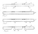
- Fig. 1 is a cross-sectional view of a semiconductor wafer array comprising a plurality of stacked wafers according to the present invention;
- Fig. 2 is a plan view of one of the wafers of Fig. 1 showing several ring-shaped electrical pads on one surface thereof;
- Fig. 3 is a cross-sectional view taken in the direction of lines 3-3 of Fig. 2;
- Fig. 4 is a cross-sectional view showing the wafer of Fig. 3 after it has been coated with an etch-resistant material;
- Fig. 5 is a cross-sectional view of the wafer of Fig. 4 after it has been patterned to expose a square area on the backside of the semiconductor wafer substrate beneath the pads;
- Fig. 6 is a cross-sectional view of the wafer of Fig. 5 showing two through-holes provided therein;
- Fig. 7 is an enlarged cross-sectional view of one of the vias shown in Fig. 6 after the etch-resistant coating shown in Figs. 4-6 is removed from the center of the ring-shaped pad surrounding the via.
- Fig. 8 is a cross-sectional view of the via of Fig. 7 after the sharp edges at the apex of the via are removed;
- Fig. 9 is a cross-sectional view of the via of Fig. 8 after its walls have been coated with an electrically insulating layer.
- Fig. 10 is a cross-sectional view of the via of Fig. 9 after the etch-resistant coating shown in Figs. 4-9 is removed from the ring-shaped pad.
- Fig. 11 is a cross-sectional view of the via of Fig. 10 after a wad of compliant electrically conductive fine wire is inserted therein;
- Fig. 12 is an enlarged partial cross-sectional view showing two wafers stacked one on top of another between a dummy wafer and a base plate with the wad of Fig. 11 inserted in each of the vias located therein according to the present invention;
- Fig. 13 is an enlarged partial cross-sectional view showing an alternative embodiment of the present invention, comprising electrically conductive compliant elastomeric material;
- Fig. 14 is an alternative embodiment of the present invention showing the top of a wad of fine wire compressed onto the pad surrounding the via; and
- Fig. 15 is a partial cross-sectional view showing relative dimensions of the vias in the wafers.
- Referring to Fig. 1, there is provided in accordance with the present invention a semiconductor wafer array designated generally as 1. In the
array 1 there is provided ahousing 2 mounted on abase plate 3. In thehousing 2 there is provided a plurality of side walls 4, 5 and 6 and a top wall 7. A front wall corresponding to side walls 4-6 is not shown. Located in thehousing 2 between thebase plate 3 and top wall 7, there is provided a stack of semiconductor wafers 10-18. In the stack of wafers 10-18, thebottom wafer 10 is located adjacent to thebase plate 3. Thetop wafers 18 is located nearest to the top wall 7. Wafer 18 may be a dummy wafer which is used simply for terminating the vertical electrical connecting members and forming an electrical connection with the pads on wafer 17 as will be further described below. On top ofwafer 18 betweenwafer 18 and top wall 17, there is provided a compliant electrically insulating thermallyconductive pad 20.Pad 20 is located between thewafer 18 and the top wall 7 to compensate for thermal expansion and contraction of the stack of wafers 10-18 and for conducting heat from the stack of wafers 10-18 to the top wall 7. Extending from the top wall 7 there is provided a plurality ofmetallic fingers 21.Fingers 21 comprise cooling fins for dissipating heat from thehousing 2. - Extending through the
base plate 3 there is provided a plurality ofelectrical pin members 22.Pin members 22 are provided for making electrical contact with electrically conductive compliant material in vias in the stack of wafers 10-18, as will be further described below. - In practice, the
base plate 3 comprises insulating material, such as ceramic material, for insulating thepin members 22 from each other, and theside wall members 2 and 4 may comprise a metallic material. The free area within thehousing 2 may be filled with a conventional electrically non-conductive gaseous or liquid material to facilitate the dissipation of heat from thehousing 2. - In each of the wafers 10-17 there is provided a plurality of hourglass-
shaped vias 25. Corresponding pyramid-shapedrecesses 26 are normally provided indummy wafer 18. In each of thevias 25 and recesses 26 there is provided awad 27 of an electrically conductive compliant material, such as, for example, a fine wire or an electrically conductive elastomer. Thevias 25 and recesses 26 in the wafers 10-18 are placed in registration with a corresponding via in an adjacent wafer, such that thewads 27 of electrically conductive compliant material in the vias combine to form a conductive vertical column providing electrical connections from feedthrough pins 22 to each of said semiconductor wafers 10-18. - While the embodiment of Fig. 1 shows a sealed
housing 2, it is understood that conventional ports for circulating cooling gases or fluids may be added to thehousing 2 in a manner as best fits the heat flow requirements of the application circuits located therein. Also, in certain applications, certain of thevias 25 may provide vertical connections between two or more but less than all of the wafers. - Referring to Figs. 2-11, the steps used for fabricating each of the semiconductive wafers in the stack of wafers 10-18 will now be described. For convenience, the description will be made with respect to
wafer 10, it being understood that the other wafers 11-17, except for possible differences in the electrical circuits provided therein, are substantially identical insofar as the present invention is concerned. - Referring to Figs. 2 and 3,
wafer 10, a 1,0,0 silicon wafer, is provided with a first ortopside surface 30 and a second orbackside surface 31. Electrical circuits, e.g. logic circuits, memory cells, or the like (not shown), are provided in thesurface 30 and laterally electrically connected to one or more ring-shaped pads 32-37. While only 6 pads are shown, it is to be understood that many such pads are normally present on each wafer. - The
surfaces wafer 10 are then provided with acoating 34 of etch-resistant material such as silicon nitride as shown in Fig. 4. After thewafer 10 has been coated with the etch-resistant material, thecoating 34 is patterned on thebackside 31 of thewafer 10 by techniques known in the microlithographic art and plasma-etched so as to providesquare openings 35 in the nitride coating exposing thewafer 10 beneath the pads 32-37 as shown in Fig. 5. After thesquare openings 35 are produced, thewafer 10 is subjected to a conventional anisotropic etch process,such as 85°C potassium hydroxide at 35% concentration, that produces a truncated pyramid-shaped hole orrecess 36 in thewafer 10 as shown in Fig. 6. Other techniques may also be used for fabricating theholes 36 such as those comprising laser means and combined laser and etch means. Any means that yields roughly pyramid-, cone- or hourglass-shaped vias, while avoiding damage to the surface of the wafer, may be used for the purpose of this invention. - Referring to Fig. 7, there is shown an enlarged cross-sectional view of the
pad 33 andhole 36 in thewafer 10. As shown in Fig. 7, the anisotropic etch process used for making theholes 36 as described above with respect to Fig. 6 produces extremely sharp and therefore somewhatfragile edges 37 which are subject to chipping and cracking. In order to remove thesharp edges 37, thesilicon nitride coating 34 in the center of thepad 33 is removed and thewafer 10 subjected to a second short anisotropic etching process. This etching process produces a second inverted truncated pyramid-shapedhole 38, thus forming square-sided hourglass-shapedvias 25 as shown in Figs. 1 and 8. - After the
vias 25 are formed in thewafer 10, an insulatinglayer 40 of silicon nitride is grown or deposited on the walls of the vias 25 so as to provide electrical isolation of thewafer 10 as shown in Fig. 9. Thereafter, thesilicon nitride coating 34 is removed from thebonding pad 33 as shown in Fig. 10. For the purpose of this disclosure, it may be assumed that the wafers 10-18 are approximately 0.448mm thick , that the aperture 41 at the top of the via 25 is approximately 0.224mm on a side and that theaperture 42 at the bottom of the via 25 is approximately 0.672mm on a side. - Referring to Fig. 11, there is provided in each of the vias 25 a wad of electrically conductive
compliant material 45. In one of the embodiments of the present invention, thewad 45 comprises a wad of single strand fine wire. The shape of thewad 45 is roughly that of a pyramid or a cone. The diameter of the wire used to make thewad 45 is approximately 1/10th that of the width of the top side aperture 41, i.e. 0.022mm and the volume of the wire used is such as to fill thevias 25 to within 10 to 20% of their volume; the remainder of the via volume comprising the air space between the wire in the wad. Any suitable conventional means may be used for pre-forming thewads 45 into the desired shape. - Referring to Fig. 12, there is shown an
assembly 50 comprising three of the wafers 10-18, namelywafers vias wafers base 3 with thevias base 3. Located on top of the stack ofwafers conductive pad 20 described above with respect to Fig. 1. Thewafers - The configuration of the
vias wads 45 as shown in Figs. 11 and 12 is an important feature of the present invention. The pyramid or cone shape of each of thewads 45 allows its base or larger end to make connection to thewafer bonding pad 33 while its apex or smaller end makes connection to the base of the next highervertical wad 45. In the case of thebottom wafer 10, the base of thewad 45 therein makes an electrical contact with thefeedthrough pin 22, as also shown in Fig. 1. In the case of thetop dummy wafer 18, thedummy wafer 18, without circuits, is used as a containment for the top level ofwads 45 so as to compress the wads and provide an electrical connection to thepad 33 on thetopmost circuit wafer 11 and theunderlying wad 45 in thewafer 11. - As an alternative to the fine wire wads 45 of Fig. 12, Fig. 13 shows a shaped form of conventional compliant
conductive elastomer 51. A plurality ofwads 51 may be used in place ofwads 45 if desired. - Referring to Fig. 14, there is provided in an alternative embodiment of the present invention a wad of electrically conductive compliant wire material 55. Wad 55 is substantially identical to wad 45 described above with respect to Figs. 11 and 12 with the exception that the wad 55 is made to extend through the
wafer 10 and aportion 56 thereof is then compressed back against thebonding ring pad 33 so as to cause the wafer to retain the mass of fine wire 55 in thevias 25 and to insure contact to thebonding ring 33. This configuration may be used in place of thewads 45 used in wafer 10-17 and, if used in wafer 17 at the top of the stack, the use of thedummy wafer 18 to insure the making of an electrical contact to thepad 33 on the wafer 17 may be avoided. - Referring to Fig. 15, the width s2 of the
vias 25 is given by the equation
s2 = s1 + √2 t - 2√2 rt
where
s1 is the width of the apex of thevias 25,
t is the thickness of thewafer 10 and
r is a constant having a value less than unity, (e.g. .1 - .2.) - While several embodiments of the present invention are described above, it is contemplated that various modifications may be made thereto without departing from the spirit and scope of the present invention. For example, the second etch described above for making the
hole 38 may be an isotropic etch thereby producing the same sized hole but with parallel sidewalls. Of course, thewads 45 may be similarly shaped. In all cases, the methods and means used for forming the vias and the wads comprise conventional semiconductor wafer processing techniques. Accordingly, it is intended that the embodiments described be considered only as illustrative of the present invention and that the scope thereof should not be limited thereto but be determined by reference to the claims hereinafter provided and their equivalents.
Claims (15)
Applications Claiming Priority (2)
| Application Number | Priority Date | Filing Date | Title |
|---|---|---|---|
| US114633 | 1987-10-28 | ||
| US07/114,633US4954875A (en) | 1986-07-17 | 1987-10-28 | Semiconductor wafer array with electrically conductive compliant material |
Publications (2)
| Publication Number | Publication Date |
|---|---|
| EP0314437A1true EP0314437A1 (en) | 1989-05-03 |
| EP0314437B1 EP0314437B1 (en) | 1992-07-15 |
Family
ID=22356470
Family Applications (1)
| Application Number | Title | Priority Date | Filing Date |
|---|---|---|---|
| EP88310029AExpiredEP0314437B1 (en) | 1987-10-28 | 1988-10-25 | Semiconductor wafer array |
Country Status (4)
| Country | Link |
|---|---|
| US (1) | US4954875A (en) |
| EP (1) | EP0314437B1 (en) |
| JP (1) | JPH0817223B2 (en) |
| DE (1) | DE3872828T2 (en) |
Cited By (51)
| Publication number | Priority date | Publication date | Assignee | Title |
|---|---|---|---|---|
| EP0374971A3 (en)* | 1988-12-23 | 1990-09-19 | Matsushita Electric Industrial Co., Ltd. | Three-dimensionally stacked lsi |
| WO1992003848A3 (en)* | 1990-08-28 | 1992-07-23 | Lsi Logic Europ | Stacking of integrated circuits |
| US5202754A (en)* | 1991-09-13 | 1993-04-13 | International Business Machines Corporation | Three-dimensional multichip packages and methods of fabrication |
| US5239447A (en)* | 1991-09-13 | 1993-08-24 | International Business Machines Corporation | Stepped electronic device package |
| US5340771A (en)* | 1993-03-18 | 1994-08-23 | Lsi Logic Corporation | Techniques for providing high I/O count connections to semiconductor dies |
| AU656595B2 (en)* | 1991-07-09 | 1995-02-09 | Hughes Aircraft Company | Stacked chip assembly and manufacturing method therefor |
| US5399898A (en)* | 1992-07-17 | 1995-03-21 | Lsi Logic Corporation | Multi-chip semiconductor arrangements using flip chip dies |
| US6096576A (en)* | 1997-09-02 | 2000-08-01 | Silicon Light Machines | Method of producing an electrical interface to an integrated circuit device having high density I/O count |
| US6098278A (en)* | 1994-06-23 | 2000-08-08 | Cubic Memory, Inc. | Method for forming conductive epoxy flip-chip on chip |
| EP1061578A4 (en)* | 1998-12-16 | 2001-07-18 | Seiko Epson Corp | SEMICONDUCTOR CHIP, SEMICONDUCTOR ARRANGEMENT, CIRCUIT BOARD AND ELECTRONIC DEVICE AND METHOD FOR THE PRODUCTION THEREOF |
| US6271598B1 (en)* | 1997-07-29 | 2001-08-07 | Cubic Memory, Inc. | Conductive epoxy flip-chip on chip |
| WO2002013268A3 (en)* | 2000-08-03 | 2002-09-12 | Bosch Gmbh Robert | Module, especially a wafer module |
| EP1233444A3 (en)* | 1992-04-08 | 2002-12-11 | LEEDY, Glenn J. | Membrane dielectric isolation ic fabrication |
| US6674161B1 (en)* | 2000-10-03 | 2004-01-06 | Rambus Inc. | Semiconductor stacked die devices |
| US6712480B1 (en) | 2002-09-27 | 2004-03-30 | Silicon Light Machines | Controlled curvature of stressed micro-structures |
| US6767751B2 (en) | 2002-05-28 | 2004-07-27 | Silicon Light Machines, Inc. | Integrated driver process flow |
| US6782205B2 (en) | 2001-06-25 | 2004-08-24 | Silicon Light Machines | Method and apparatus for dynamic equalization in wavelength division multiplexing |
| US6785001B2 (en) | 2001-08-21 | 2004-08-31 | Silicon Light Machines, Inc. | Method and apparatus for measuring wavelength jitter of light signal |
| US6801354B1 (en) | 2002-08-20 | 2004-10-05 | Silicon Light Machines, Inc. | 2-D diffraction grating for substantially eliminating polarization dependent losses |
| US6800238B1 (en) | 2002-01-15 | 2004-10-05 | Silicon Light Machines, Inc. | Method for domain patterning in low coercive field ferroelectrics |
| US6806997B1 (en) | 2003-02-28 | 2004-10-19 | Silicon Light Machines, Inc. | Patterned diffractive light modulator ribbon for PDL reduction |
| US6813059B2 (en) | 2002-06-28 | 2004-11-02 | Silicon Light Machines, Inc. | Reduced formation of asperities in contact micro-structures |
| US6822797B1 (en) | 2002-05-31 | 2004-11-23 | Silicon Light Machines, Inc. | Light modulator structure for producing high-contrast operation using zero-order light |
| US6829092B2 (en) | 2001-08-15 | 2004-12-07 | Silicon Light Machines, Inc. | Blazed grating light valve |
| US6829077B1 (en) | 2003-02-28 | 2004-12-07 | Silicon Light Machines, Inc. | Diffractive light modulator with dynamically rotatable diffraction plane |
| US6839479B2 (en) | 2002-05-29 | 2005-01-04 | Silicon Light Machines Corporation | Optical switch |
| US6872984B1 (en) | 1998-07-29 | 2005-03-29 | Silicon Light Machines Corporation | Method of sealing a hermetic lid to a semiconductor die at an angle |
| US6908201B2 (en) | 2002-06-28 | 2005-06-21 | Silicon Light Machines Corporation | Micro-support structures |
| US6922273B1 (en) | 2003-02-28 | 2005-07-26 | Silicon Light Machines Corporation | PDL mitigation structure for diffractive MEMS and gratings |
| US6922272B1 (en) | 2003-02-14 | 2005-07-26 | Silicon Light Machines Corporation | Method and apparatus for leveling thermal stress variations in multi-layer MEMS devices |
| US6928207B1 (en) | 2002-12-12 | 2005-08-09 | Silicon Light Machines Corporation | Apparatus for selectively blocking WDM channels |
| US6927891B1 (en) | 2002-12-23 | 2005-08-09 | Silicon Light Machines Corporation | Tilt-able grating plane for improved crosstalk in 1×N blaze switches |
| US6934070B1 (en) | 2002-12-18 | 2005-08-23 | Silicon Light Machines Corporation | Chirped optical MEM device |
| US6947613B1 (en) | 2003-02-11 | 2005-09-20 | Silicon Light Machines Corporation | Wavelength selective switch and equalizer |
| US6956995B1 (en) | 2001-11-09 | 2005-10-18 | Silicon Light Machines Corporation | Optical communication arrangement |
| US6987600B1 (en) | 2002-12-17 | 2006-01-17 | Silicon Light Machines Corporation | Arbitrary phase profile for better equalization in dynamic gain equalizer |
| US7027202B1 (en) | 2003-02-28 | 2006-04-11 | Silicon Light Machines Corp | Silicon substrate as a light modulator sacrificial layer |
| US7042611B1 (en) | 2003-03-03 | 2006-05-09 | Silicon Light Machines Corporation | Pre-deflected bias ribbons |
| US7046420B1 (en) | 2003-02-28 | 2006-05-16 | Silicon Light Machines Corporation | MEM micro-structures and methods of making the same |
| US7049164B2 (en) | 2001-09-13 | 2006-05-23 | Silicon Light Machines Corporation | Microelectronic mechanical system and methods |
| US7054515B1 (en) | 2002-05-30 | 2006-05-30 | Silicon Light Machines Corporation | Diffractive light modulator-based dynamic equalizer with integrated spectral monitor |
| US7057795B2 (en) | 2002-08-20 | 2006-06-06 | Silicon Light Machines Corporation | Micro-structures with individually addressable ribbon pairs |
| US7057819B1 (en) | 2002-12-17 | 2006-06-06 | Silicon Light Machines Corporation | High contrast tilting ribbon blazed grating |
| US7068372B1 (en) | 2003-01-28 | 2006-06-27 | Silicon Light Machines Corporation | MEMS interferometer-based reconfigurable optical add-and-drop multiplexor |
| US7177081B2 (en) | 2001-03-08 | 2007-02-13 | Silicon Light Machines Corporation | High contrast grating light valve type device |
| US7215018B2 (en) | 2004-04-13 | 2007-05-08 | Vertical Circuits, Inc. | Stacked die BGA or LGA component assembly |
| US7245021B2 (en) | 2004-04-13 | 2007-07-17 | Vertical Circuits, Inc. | Micropede stacked die component assembly |
| US7286764B1 (en) | 2003-02-03 | 2007-10-23 | Silicon Light Machines Corporation | Reconfigurable modulator-based optical add-and-drop multiplexer |
| US7391973B1 (en) | 2003-02-28 | 2008-06-24 | Silicon Light Machines Corporation | Two-stage gain equalizer |
| US8309396B2 (en)* | 2009-01-26 | 2012-11-13 | Taiwan Semiconductor Manufacturing Company, Ltd. | System and method for 3D integrated circuit stacking |
| CN110008490A (en)* | 2015-03-17 | 2019-07-12 | 英飞凌科技奥地利有限公司 | System and method for dual zone segmentation |
Families Citing this family (107)
| Publication number | Priority date | Publication date | Assignee | Title |
|---|---|---|---|---|
| US5140405A (en)* | 1990-08-30 | 1992-08-18 | Micron Technology, Inc. | Semiconductor assembly utilizing elastomeric single axis conductive interconnect |
| US5229647A (en)* | 1991-03-27 | 1993-07-20 | Micron Technology, Inc. | High density data storage using stacked wafers |
| US6714625B1 (en) | 1992-04-08 | 2004-03-30 | Elm Technology Corporation | Lithography device for semiconductor circuit pattern generation |
| US5432999A (en)* | 1992-08-20 | 1995-07-18 | Capps; David F. | Integrated circuit lamination process |
| US5424245A (en)* | 1994-01-04 | 1995-06-13 | Motorola, Inc. | Method of forming vias through two-sided substrate |
| US6080596A (en)* | 1994-06-23 | 2000-06-27 | Cubic Memory Inc. | Method for forming vertical interconnect process for silicon segments with dielectric isolation |
| US5698895A (en)* | 1994-06-23 | 1997-12-16 | Cubic Memory, Inc. | Silicon segment programming method and apparatus |
| US6486528B1 (en) | 1994-06-23 | 2002-11-26 | Vertical Circuits, Inc. | Silicon segment programming apparatus and three terminal fuse configuration |
| US5675180A (en)* | 1994-06-23 | 1997-10-07 | Cubic Memory, Inc. | Vertical interconnect process for silicon segments |
| US5891761A (en)* | 1994-06-23 | 1999-04-06 | Cubic Memory, Inc. | Method for forming vertical interconnect process for silicon segments with thermally conductive epoxy preform |
| US6255726B1 (en) | 1994-06-23 | 2001-07-03 | Cubic Memory, Inc. | Vertical interconnect process for silicon segments with dielectric isolation |
| US6124633A (en)* | 1994-06-23 | 2000-09-26 | Cubic Memory | Vertical interconnect process for silicon segments with thermally conductive epoxy preform |
| MY114888A (en)* | 1994-08-22 | 2003-02-28 | Ibm | Method for forming a monolithic electronic module by stacking planar arrays of integrated circuit chips |
| US5949029A (en)* | 1994-08-23 | 1999-09-07 | Thomas & Betts International, Inc. | Conductive elastomers and methods for fabricating the same |
| US5599193A (en)* | 1994-08-23 | 1997-02-04 | Augat Inc. | Resilient electrical interconnect |
| DE4433845A1 (en)* | 1994-09-22 | 1996-03-28 | Fraunhofer Ges Forschung | Method of manufacturing a three-dimensional integrated circuit |
| DE4433833A1 (en)* | 1994-09-22 | 1996-03-28 | Fraunhofer Ges Forschung | Method for producing a three-dimensional integrated circuit while achieving high system yields |
| DE4435121A1 (en)* | 1994-09-30 | 1996-04-04 | Siemens Ag | Portable data carrier arrangement operable on data bus |
| US5668409A (en)* | 1995-06-05 | 1997-09-16 | Harris Corporation | Integrated circuit with edge connections and method |
| US5682062A (en)* | 1995-06-05 | 1997-10-28 | Harris Corporation | System for interconnecting stacked integrated circuits |
| US5608264A (en)* | 1995-06-05 | 1997-03-04 | Harris Corporation | Surface mountable integrated circuit with conductive vias |
| US5814889A (en)* | 1995-06-05 | 1998-09-29 | Harris Corporation | Intergrated circuit with coaxial isolation and method |
| US5618752A (en)* | 1995-06-05 | 1997-04-08 | Harris Corporation | Method of fabrication of surface mountable integrated circuits |
| US5646067A (en)* | 1995-06-05 | 1997-07-08 | Harris Corporation | Method of bonding wafers having vias including conductive material |
| US5770884A (en)* | 1995-06-30 | 1998-06-23 | International Business Machines Corporation | Very dense integrated circuit package |
| EP1503406A3 (en)* | 1996-10-29 | 2009-07-08 | Tru-Si Technologies, Inc. | Back-side contact pads of a semiconductor chip |
| US5915167A (en) | 1997-04-04 | 1999-06-22 | Elm Technology Corporation | Three dimensional structure memory |
| US6551857B2 (en) | 1997-04-04 | 2003-04-22 | Elm Technology Corporation | Three dimensional structure integrated circuits |
| JPH1123615A (en)* | 1997-05-09 | 1999-01-29 | Hitachi Ltd | Connection device and inspection system |
| JP2001514449A (en)* | 1997-08-22 | 2001-09-11 | キュービック・メモリー・インコーポレーテッド | Vertical interconnect method of silicon segments with thermally conductive epoxy preform |
| US6087199A (en)* | 1998-02-04 | 2000-07-11 | International Business Machines Corporation | Method for fabricating a very dense chip package |
| US5998868A (en)* | 1998-02-04 | 1999-12-07 | International Business Machines Corporation | Very dense chip package |
| US6025638A (en)* | 1998-06-01 | 2000-02-15 | International Business Machines Corporation | Structure for precision multichip assembly |
| US6614095B1 (en) | 1998-06-04 | 2003-09-02 | Gfd-Gesellschaft Fur Diamantprodukte Mbh | Diamond component with rear side contact and a method for the production thereof |
| US6429509B1 (en)* | 1999-05-03 | 2002-08-06 | United Microelectronics Corporation | Integrated circuit with improved interconnect structure and process for making same |
| US6333553B1 (en) | 1999-05-21 | 2001-12-25 | International Business Machines Corporation | Wafer thickness compensation for interchip planarity |
| JP3750444B2 (en)* | 1999-10-22 | 2006-03-01 | セイコーエプソン株式会社 | Manufacturing method of semiconductor device |
| US6710454B1 (en) | 2000-02-16 | 2004-03-23 | Micron Technology, Inc. | Adhesive layer for an electronic apparatus having multiple semiconductor devices |
| JP2001352035A (en)* | 2000-06-07 | 2001-12-21 | Sony Corp | Assembling jig for multilayer semiconductor device and manufacturing method therefor |
| TW483129B (en)* | 2000-10-05 | 2002-04-11 | Amkor Technology Taiwan Linkou | Package for image sensing device and its manufacturing process |
| US7129113B1 (en) | 2000-10-13 | 2006-10-31 | Bridge Semiconductor Corporation | Method of making a three-dimensional stacked semiconductor package with a metal pillar in an encapsulant aperture |
| US7009297B1 (en) | 2000-10-13 | 2006-03-07 | Bridge Semiconductor Corporation | Semiconductor chip assembly with embedded metal particle |
| US7262082B1 (en) | 2000-10-13 | 2007-08-28 | Bridge Semiconductor Corporation | Method of making a three-dimensional stacked semiconductor package with a metal pillar and a conductive interconnect in an encapsulant aperture |
| US6840777B2 (en)* | 2000-11-30 | 2005-01-11 | Intel Corporation | Solderless electronics packaging |
| JP2002270718A (en)* | 2001-03-07 | 2002-09-20 | Seiko Epson Corp | Wiring board and its manufacturing method, semiconductor device and its manufacturing method, circuit board, and electronic equipment |
| US6451626B1 (en) | 2001-07-27 | 2002-09-17 | Charles W.C. Lin | Three-dimensional stacked semiconductor package |
| US6765287B1 (en) | 2001-07-27 | 2004-07-20 | Charles W. C. Lin | Three-dimensional stacked semiconductor package |
| US6486549B1 (en) | 2001-11-10 | 2002-11-26 | Bridge Semiconductor Corporation | Semiconductor module with encapsulant base |
| US7190060B1 (en) | 2002-01-09 | 2007-03-13 | Bridge Semiconductor Corporation | Three-dimensional stacked semiconductor package device with bent and flat leads and method of making same |
| SG104293A1 (en)* | 2002-01-09 | 2004-06-21 | Micron Technology Inc | Elimination of rdl using tape base flip chip on flex for die stacking |
| US6891276B1 (en) | 2002-01-09 | 2005-05-10 | Bridge Semiconductor Corporation | Semiconductor package device |
| US6661085B2 (en)* | 2002-02-06 | 2003-12-09 | Intel Corporation | Barrier structure against corrosion and contamination in three-dimensional (3-D) wafer-to-wafer vertical stack |
| US6762076B2 (en)* | 2002-02-20 | 2004-07-13 | Intel Corporation | Process of vertically stacking multiple wafers supporting different active integrated circuit (IC) devices |
| US6668748B2 (en)* | 2002-03-01 | 2003-12-30 | H2Eye (International) Limited | Submersible articles and method of manufacture thereof |
| SG111935A1 (en) | 2002-03-04 | 2005-06-29 | Micron Technology Inc | Interposer configured to reduce the profiles of semiconductor device assemblies and packages including the same and methods |
| SG115455A1 (en) | 2002-03-04 | 2005-10-28 | Micron Technology Inc | Methods for assembly and packaging of flip chip configured dice with interposer |
| SG115459A1 (en)* | 2002-03-04 | 2005-10-28 | Micron Technology Inc | Flip chip packaging using recessed interposer terminals |
| SG121707A1 (en) | 2002-03-04 | 2006-05-26 | Micron Technology Inc | Method and apparatus for flip-chip packaging providing testing capability |
| SG115456A1 (en) | 2002-03-04 | 2005-10-28 | Micron Technology Inc | Semiconductor die packages with recessed interconnecting structures and methods for assembling the same |
| TWI232560B (en)* | 2002-04-23 | 2005-05-11 | Sanyo Electric Co | Semiconductor device and its manufacture |
| TWI229435B (en) | 2002-06-18 | 2005-03-11 | Sanyo Electric Co | Manufacture of semiconductor device |
| AU2003255254A1 (en) | 2002-08-08 | 2004-02-25 | Glenn J. Leedy | Vertical system integration |
| US20040036170A1 (en) | 2002-08-20 | 2004-02-26 | Lee Teck Kheng | Double bumping of flexible substrate for first and second level interconnects |
| JP3828473B2 (en)* | 2002-09-30 | 2006-10-04 | 株式会社東芝 | Multilayer semiconductor device and manufacturing method thereof |
| TWI227550B (en)* | 2002-10-30 | 2005-02-01 | Sanyo Electric Co | Semiconductor device manufacturing method |
| TW569416B (en)* | 2002-12-19 | 2004-01-01 | Via Tech Inc | High density multi-chip module structure and manufacturing method thereof |
| US7354798B2 (en)* | 2002-12-20 | 2008-04-08 | International Business Machines Corporation | Three-dimensional device fabrication method |
| JP4401181B2 (en)* | 2003-08-06 | 2010-01-20 | 三洋電機株式会社 | Semiconductor device and manufacturing method thereof |
| US7183654B2 (en)* | 2003-09-30 | 2007-02-27 | Intel Corporation | Providing a via with an increased via contact area |
| US7993983B1 (en) | 2003-11-17 | 2011-08-09 | Bridge Semiconductor Corporation | Method of making a semiconductor chip assembly with chip and encapsulant grinding |
| US7122462B2 (en)* | 2003-11-21 | 2006-10-17 | International Business Machines Corporation | Back end interconnect with a shaped interface |
| US7227249B1 (en) | 2003-12-24 | 2007-06-05 | Bridge Semiconductor Corporation | Three-dimensional stacked semiconductor package with chips on opposite sides of lead |
| US7705432B2 (en)* | 2004-04-13 | 2010-04-27 | Vertical Circuits, Inc. | Three dimensional six surface conformal die coating |
| DE102004031878B3 (en)* | 2004-07-01 | 2005-10-06 | Epcos Ag | Electrical multilayer component with reliable solder contact |
| US7087538B2 (en)* | 2004-08-16 | 2006-08-08 | Intel Corporation | Method to fill the gap between coupled wafers |
| KR20070009136A (en)* | 2005-07-15 | 2007-01-18 | 삼성전자주식회사 | A packaging chip comprising a through electrode directly connected to a plurality of wafers and a manufacturing method thereof |
| US7622313B2 (en)* | 2005-07-29 | 2009-11-24 | Freescale Semiconductor, Inc. | Fabrication of three dimensional integrated circuit employing multiple die panels |
| US7307348B2 (en)* | 2005-12-07 | 2007-12-11 | Micron Technology, Inc. | Semiconductor components having through wire interconnects (TWI) |
| TWI324800B (en)* | 2005-12-28 | 2010-05-11 | Sanyo Electric Co | Method for manufacturing semiconductor device |
| TW200737506A (en)* | 2006-03-07 | 2007-10-01 | Sanyo Electric Co | Semiconductor device and manufacturing method of the same |
| US7659612B2 (en) | 2006-04-24 | 2010-02-09 | Micron Technology, Inc. | Semiconductor components having encapsulated through wire interconnects (TWI) |
| US8581380B2 (en)* | 2006-07-10 | 2013-11-12 | Stats Chippac Ltd. | Integrated circuit packaging system with ultra-thin die |
| JP5258567B2 (en)* | 2006-08-11 | 2013-08-07 | セミコンダクター・コンポーネンツ・インダストリーズ・リミテッド・ライアビリティ・カンパニー | Semiconductor device and manufacturing method thereof |
| US8513789B2 (en) | 2006-10-10 | 2013-08-20 | Tessera, Inc. | Edge connect wafer level stacking with leads extending along edges |
| US7901989B2 (en) | 2006-10-10 | 2011-03-08 | Tessera, Inc. | Reconstituted wafer level stacking |
| US7829438B2 (en) | 2006-10-10 | 2010-11-09 | Tessera, Inc. | Edge connect wafer level stacking |
| US7494843B1 (en) | 2006-12-26 | 2009-02-24 | Bridge Semiconductor Corporation | Method of making a semiconductor chip assembly with thermal conductor and encapsulant grinding |
| US7811863B1 (en) | 2006-10-26 | 2010-10-12 | Bridge Semiconductor Corporation | Method of making a semiconductor chip assembly with metal pillar and encapsulant grinding and heat sink attachment |
| JP5010247B2 (en)* | 2006-11-20 | 2012-08-29 | オンセミコンダクター・トレーディング・リミテッド | Semiconductor device and manufacturing method thereof |
| US20080157322A1 (en)* | 2006-12-27 | 2008-07-03 | Jia Miao Tang | Double side stacked die package |
| US7952195B2 (en)* | 2006-12-28 | 2011-05-31 | Tessera, Inc. | Stacked packages with bridging traces |
| JP5572089B2 (en) | 2007-07-27 | 2014-08-13 | テッセラ,インコーポレイテッド | Reconfigured wafer stack packaging with pad extension after application |
| US8551815B2 (en) | 2007-08-03 | 2013-10-08 | Tessera, Inc. | Stack packages using reconstituted wafers |
| US8043895B2 (en)* | 2007-08-09 | 2011-10-25 | Tessera, Inc. | Method of fabricating stacked assembly including plurality of stacked microelectronic elements |
| US7834462B2 (en)* | 2007-09-17 | 2010-11-16 | Qimonda Ag | Electric device, stack of electric devices, and method of manufacturing a stack of electric devices |
| US8017451B2 (en) | 2008-04-04 | 2011-09-13 | The Charles Stark Draper Laboratory, Inc. | Electronic modules and methods for forming the same |
| US8273603B2 (en) | 2008-04-04 | 2012-09-25 | The Charles Stark Draper Laboratory, Inc. | Interposers, electronic modules, and methods for forming the same |
| US7683459B2 (en)* | 2008-06-02 | 2010-03-23 | Hong Kong Applied Science and Technology Research Institute Company, Ltd. | Bonding method for through-silicon-via based 3D wafer stacking |
| JP5639052B2 (en)* | 2008-06-16 | 2014-12-10 | テッセラ,インコーポレイテッド | Edge stacking at wafer level |
| US7948072B2 (en)* | 2008-07-25 | 2011-05-24 | Industrial Technology Research Institute | Wafer-to-wafer stacking |
| JP4985618B2 (en)* | 2008-11-07 | 2012-07-25 | 富士電機株式会社 | Solder joining method |
| US8159065B2 (en) | 2009-03-06 | 2012-04-17 | Hynix Semiconductor Inc. | Semiconductor package having an internal cooling system |
| WO2010104610A2 (en)* | 2009-03-13 | 2010-09-16 | Tessera Technologies Hungary Kft. | Stacked microelectronic assemblies having vias extending through bond pads |
| JP5128712B1 (en)* | 2012-04-13 | 2013-01-23 | ラピスセミコンダクタ株式会社 | Semiconductor device |
| TWI559465B (en)* | 2015-08-14 | 2016-11-21 | 恆勁科技股份有限公司 | Package substrate and its fabrication method |
| CN120359356A (en) | 2023-04-28 | 2025-07-22 | 株式会社Ihi | Rotary machine |
| US20240421076A1 (en)* | 2023-06-13 | 2024-12-19 | International Business Machines Corporation | Advanced interconnects with hyperboloid profile |
Citations (5)
| Publication number | Priority date | Publication date | Assignee | Title |
|---|---|---|---|---|
| FR2012333A1 (en)* | 1968-07-05 | 1970-03-20 | Ibm | |
| DE3233195A1 (en)* | 1981-09-08 | 1983-03-17 | Mitsubishi Denki K.K., Tokyo | Semiconductor device |
| GB2150749A (en)* | 1983-12-03 | 1985-07-03 | Standard Telephones Cables Ltd | Integrated circuits |
| US4574331A (en)* | 1983-05-31 | 1986-03-04 | Trw Inc. | Multi-element circuit construction |
| EP0206696A2 (en)* | 1985-06-17 | 1986-12-30 | Fujitsu Limited | Multi-layer semiconductor device |
Family Cites Families (27)
| Publication number | Priority date | Publication date | Assignee | Title |
|---|---|---|---|---|
| US2627545A (en)* | 1950-08-19 | 1953-02-03 | Westinghouse Electric Corp | Semiconductor device |
| US2734154A (en)* | 1953-07-27 | 1956-02-07 | Semiconductor devices | |
| US3197766A (en)* | 1962-03-08 | 1965-07-27 | Control Data Corp | Stacked circuit boards |
| US3561110A (en)* | 1967-08-31 | 1971-02-09 | Ibm | Method of making connections and conductive paths |
| US3475660A (en)* | 1967-12-01 | 1969-10-28 | Int Rectifier Corp | Hollow cylindrical semiconductor device |
| US3648131A (en)* | 1969-11-07 | 1972-03-07 | Ibm | Hourglass-shaped conductive connection through semiconductor structures |
| US3704455A (en)* | 1971-02-01 | 1972-11-28 | Alfred D Scarbrough | 3d-coaxial memory construction and method of making |
| US3813773A (en)* | 1972-09-05 | 1974-06-04 | Bunker Ramo | Method employing precision stamping for fabricating the wafers of a multiwafer electrical circuit structure |
| GB1431185A (en)* | 1972-10-31 | 1976-04-07 | Int Computers Ltd | Electrical connectors and to methods for making electrical connec tors |
| US3904934A (en)* | 1973-03-26 | 1975-09-09 | Massachusetts Inst Technology | Interconnection of planar electronic structures |
| US3867759A (en)* | 1973-06-13 | 1975-02-25 | Us Air Force | Method of manufacturing a multi-layered strip transmission line printed circuit board integrated package |
| US3999105A (en)* | 1974-04-19 | 1976-12-21 | International Business Machines Corporation | Liquid encapsulated integrated circuit package |
| US3967162A (en)* | 1974-07-24 | 1976-06-29 | Amp Incorporated | Interconnection of oppositely disposed circuit devices |
| CS169520B1 (en)* | 1974-09-05 | 1976-07-29 | ||
| US4050756A (en)* | 1975-12-22 | 1977-09-27 | International Telephone And Telegraph Corporation | Conductive elastomer connector and method of making same |
| CS182611B1 (en)* | 1976-03-18 | 1978-04-28 | Pavel Reichel | Power semiconducting element |
| US4029375A (en)* | 1976-06-14 | 1977-06-14 | Electronic Engineering Company Of California | Miniature electrical connector |
| JPS5555985U (en)* | 1978-10-12 | 1980-04-16 | ||
| JPS56116282A (en)* | 1980-02-19 | 1981-09-11 | Sharp Kk | Electronic part with plural terminals |
| US4368106A (en)* | 1980-10-27 | 1983-01-11 | General Electric Company | Implantation of electrical feed-through conductors |
| US4437109A (en)* | 1980-11-07 | 1984-03-13 | General Electric Company | Silicon-on-sapphire body with conductive paths therethrough |
| US4499655A (en)* | 1981-03-18 | 1985-02-19 | General Electric Company | Method for making alignment-enhancing feed-through conductors for stackable silicon-on-sapphire |
| US4394712A (en)* | 1981-03-18 | 1983-07-19 | General Electric Company | Alignment-enhancing feed-through conductors for stackable silicon-on-sapphire wafers |
| JPS5920683U (en)* | 1982-07-29 | 1984-02-08 | 松下電器産業株式会社 | Display devices for electronic equipment, etc. |
| JPS59127856A (en)* | 1983-01-12 | 1984-07-23 | Nec Corp | Semiconductor integrated circuit device with multiple layered semiconductor chip |
| US4581679A (en)* | 1983-05-31 | 1986-04-08 | Trw Inc. | Multi-element circuit construction |
| US4596069A (en)* | 1984-07-13 | 1986-06-24 | Texas Instruments Incorporated | Three dimensional processing for monolithic IMPATTs |
- 1987
- 1987-10-28USUS07/114,633patent/US4954875A/ennot_activeExpired - Fee Related
- 1988
- 1988-10-25EPEP88310029Apatent/EP0314437B1/ennot_activeExpired
- 1988-10-25DEDE8888310029Tpatent/DE3872828T2/ennot_activeExpired - Fee Related
- 1988-10-27JPJP63271951Apatent/JPH0817223B2/ennot_activeExpired - Lifetime
Patent Citations (5)
| Publication number | Priority date | Publication date | Assignee | Title |
|---|---|---|---|---|
| FR2012333A1 (en)* | 1968-07-05 | 1970-03-20 | Ibm | |
| DE3233195A1 (en)* | 1981-09-08 | 1983-03-17 | Mitsubishi Denki K.K., Tokyo | Semiconductor device |
| US4574331A (en)* | 1983-05-31 | 1986-03-04 | Trw Inc. | Multi-element circuit construction |
| GB2150749A (en)* | 1983-12-03 | 1985-07-03 | Standard Telephones Cables Ltd | Integrated circuits |
| EP0206696A2 (en)* | 1985-06-17 | 1986-12-30 | Fujitsu Limited | Multi-layer semiconductor device |
Non-Patent Citations (1)
| Title |
|---|
| IBM TECHNICAL DISCLOSURE BULLETIN, vol. 19, no. 18, January 1977, pages 3046-3047, New York, US; J. PARISI: "Decoupling capacitor placement"* |
Cited By (60)
| Publication number | Priority date | Publication date | Assignee | Title |
|---|---|---|---|---|
| US5191405A (en)* | 1988-12-23 | 1993-03-02 | Matsushita Electric Industrial Co., Ltd. | Three-dimensional stacked lsi |
| EP0374971A3 (en)* | 1988-12-23 | 1990-09-19 | Matsushita Electric Industrial Co., Ltd. | Three-dimensionally stacked lsi |
| WO1992003848A3 (en)* | 1990-08-28 | 1992-07-23 | Lsi Logic Europ | Stacking of integrated circuits |
| AU656595B2 (en)* | 1991-07-09 | 1995-02-09 | Hughes Aircraft Company | Stacked chip assembly and manufacturing method therefor |
| US5202754A (en)* | 1991-09-13 | 1993-04-13 | International Business Machines Corporation | Three-dimensional multichip packages and methods of fabrication |
| US5239447A (en)* | 1991-09-13 | 1993-08-24 | International Business Machines Corporation | Stepped electronic device package |
| EP1233444A3 (en)* | 1992-04-08 | 2002-12-11 | LEEDY, Glenn J. | Membrane dielectric isolation ic fabrication |
| US5399898A (en)* | 1992-07-17 | 1995-03-21 | Lsi Logic Corporation | Multi-chip semiconductor arrangements using flip chip dies |
| US5340771A (en)* | 1993-03-18 | 1994-08-23 | Lsi Logic Corporation | Techniques for providing high I/O count connections to semiconductor dies |
| US6098278A (en)* | 1994-06-23 | 2000-08-08 | Cubic Memory, Inc. | Method for forming conductive epoxy flip-chip on chip |
| US6271598B1 (en)* | 1997-07-29 | 2001-08-07 | Cubic Memory, Inc. | Conductive epoxy flip-chip on chip |
| US6096576A (en)* | 1997-09-02 | 2000-08-01 | Silicon Light Machines | Method of producing an electrical interface to an integrated circuit device having high density I/O count |
| US6452260B1 (en) | 1997-09-02 | 2002-09-17 | Silicon Light Machines | Electrical interface to integrated circuit device having high density I/O count |
| US6872984B1 (en) | 1998-07-29 | 2005-03-29 | Silicon Light Machines Corporation | Method of sealing a hermetic lid to a semiconductor die at an angle |
| US6424048B1 (en) | 1998-12-16 | 2002-07-23 | Seiko Epson Corporation | Semiconductor chip, semiconductor device, circuit board and electronic equipment and production methods for them |
| EP1061578A4 (en)* | 1998-12-16 | 2001-07-18 | Seiko Epson Corp | SEMICONDUCTOR CHIP, SEMICONDUCTOR ARRANGEMENT, CIRCUIT BOARD AND ELECTRONIC DEVICE AND METHOD FOR THE PRODUCTION THEREOF |
| US6677237B2 (en) | 1998-12-16 | 2004-01-13 | Seiko Epson Corporation | Semiconductor chip, semiconductor device, circuit board and electronic equipment and production methods for them |
| WO2002013268A3 (en)* | 2000-08-03 | 2002-09-12 | Bosch Gmbh Robert | Module, especially a wafer module |
| US6902953B2 (en) | 2000-10-03 | 2005-06-07 | Rambus Inc. | Methods of forming semiconductor stacked die devices |
| US7078790B2 (en) | 2000-10-03 | 2006-07-18 | Rambus, Inc. | Semiconductor stacked die devices and methods of forming semiconductor stacked die devices |
| US6674161B1 (en)* | 2000-10-03 | 2004-01-06 | Rambus Inc. | Semiconductor stacked die devices |
| US7177081B2 (en) | 2001-03-08 | 2007-02-13 | Silicon Light Machines Corporation | High contrast grating light valve type device |
| US6782205B2 (en) | 2001-06-25 | 2004-08-24 | Silicon Light Machines | Method and apparatus for dynamic equalization in wavelength division multiplexing |
| US6829092B2 (en) | 2001-08-15 | 2004-12-07 | Silicon Light Machines, Inc. | Blazed grating light valve |
| US6785001B2 (en) | 2001-08-21 | 2004-08-31 | Silicon Light Machines, Inc. | Method and apparatus for measuring wavelength jitter of light signal |
| US7049164B2 (en) | 2001-09-13 | 2006-05-23 | Silicon Light Machines Corporation | Microelectronic mechanical system and methods |
| US6956995B1 (en) | 2001-11-09 | 2005-10-18 | Silicon Light Machines Corporation | Optical communication arrangement |
| US6800238B1 (en) | 2002-01-15 | 2004-10-05 | Silicon Light Machines, Inc. | Method for domain patterning in low coercive field ferroelectrics |
| US6767751B2 (en) | 2002-05-28 | 2004-07-27 | Silicon Light Machines, Inc. | Integrated driver process flow |
| US6839479B2 (en) | 2002-05-29 | 2005-01-04 | Silicon Light Machines Corporation | Optical switch |
| US7054515B1 (en) | 2002-05-30 | 2006-05-30 | Silicon Light Machines Corporation | Diffractive light modulator-based dynamic equalizer with integrated spectral monitor |
| US6822797B1 (en) | 2002-05-31 | 2004-11-23 | Silicon Light Machines, Inc. | Light modulator structure for producing high-contrast operation using zero-order light |
| US6813059B2 (en) | 2002-06-28 | 2004-11-02 | Silicon Light Machines, Inc. | Reduced formation of asperities in contact micro-structures |
| US6908201B2 (en) | 2002-06-28 | 2005-06-21 | Silicon Light Machines Corporation | Micro-support structures |
| US7057795B2 (en) | 2002-08-20 | 2006-06-06 | Silicon Light Machines Corporation | Micro-structures with individually addressable ribbon pairs |
| US6801354B1 (en) | 2002-08-20 | 2004-10-05 | Silicon Light Machines, Inc. | 2-D diffraction grating for substantially eliminating polarization dependent losses |
| US6712480B1 (en) | 2002-09-27 | 2004-03-30 | Silicon Light Machines | Controlled curvature of stressed micro-structures |
| US6928207B1 (en) | 2002-12-12 | 2005-08-09 | Silicon Light Machines Corporation | Apparatus for selectively blocking WDM channels |
| US7057819B1 (en) | 2002-12-17 | 2006-06-06 | Silicon Light Machines Corporation | High contrast tilting ribbon blazed grating |
| US6987600B1 (en) | 2002-12-17 | 2006-01-17 | Silicon Light Machines Corporation | Arbitrary phase profile for better equalization in dynamic gain equalizer |
| US6934070B1 (en) | 2002-12-18 | 2005-08-23 | Silicon Light Machines Corporation | Chirped optical MEM device |
| US6927891B1 (en) | 2002-12-23 | 2005-08-09 | Silicon Light Machines Corporation | Tilt-able grating plane for improved crosstalk in 1×N blaze switches |
| US7068372B1 (en) | 2003-01-28 | 2006-06-27 | Silicon Light Machines Corporation | MEMS interferometer-based reconfigurable optical add-and-drop multiplexor |
| US7286764B1 (en) | 2003-02-03 | 2007-10-23 | Silicon Light Machines Corporation | Reconfigurable modulator-based optical add-and-drop multiplexer |
| US6947613B1 (en) | 2003-02-11 | 2005-09-20 | Silicon Light Machines Corporation | Wavelength selective switch and equalizer |
| US6922272B1 (en) | 2003-02-14 | 2005-07-26 | Silicon Light Machines Corporation | Method and apparatus for leveling thermal stress variations in multi-layer MEMS devices |
| US7046420B1 (en) | 2003-02-28 | 2006-05-16 | Silicon Light Machines Corporation | MEM micro-structures and methods of making the same |
| US6829077B1 (en) | 2003-02-28 | 2004-12-07 | Silicon Light Machines, Inc. | Diffractive light modulator with dynamically rotatable diffraction plane |
| US7391973B1 (en) | 2003-02-28 | 2008-06-24 | Silicon Light Machines Corporation | Two-stage gain equalizer |
| US7027202B1 (en) | 2003-02-28 | 2006-04-11 | Silicon Light Machines Corp | Silicon substrate as a light modulator sacrificial layer |
| US6922273B1 (en) | 2003-02-28 | 2005-07-26 | Silicon Light Machines Corporation | PDL mitigation structure for diffractive MEMS and gratings |
| US6806997B1 (en) | 2003-02-28 | 2004-10-19 | Silicon Light Machines, Inc. | Patterned diffractive light modulator ribbon for PDL reduction |
| US7042611B1 (en) | 2003-03-03 | 2006-05-09 | Silicon Light Machines Corporation | Pre-deflected bias ribbons |
| US7245021B2 (en) | 2004-04-13 | 2007-07-17 | Vertical Circuits, Inc. | Micropede stacked die component assembly |
| US7215018B2 (en) | 2004-04-13 | 2007-05-08 | Vertical Circuits, Inc. | Stacked die BGA or LGA component assembly |
| US7535109B2 (en) | 2004-04-13 | 2009-05-19 | Vertical Circuits, Inc. | Die assembly having electrical interconnect |
| US8729690B2 (en) | 2004-04-13 | 2014-05-20 | Invensas Corporation | Assembly having stacked die mounted on substrate |
| US8309396B2 (en)* | 2009-01-26 | 2012-11-13 | Taiwan Semiconductor Manufacturing Company, Ltd. | System and method for 3D integrated circuit stacking |
| CN110008490A (en)* | 2015-03-17 | 2019-07-12 | 英飞凌科技奥地利有限公司 | System and method for dual zone segmentation |
| CN110008490B (en)* | 2015-03-17 | 2022-11-25 | 英飞凌科技奥地利有限公司 | System and method for dual region segmentation |
Also Published As
| Publication number | Publication date |
|---|---|
| DE3872828T2 (en) | 1993-02-11 |
| JPH0817223B2 (en) | 1996-02-21 |
| JPH021152A (en) | 1990-01-05 |
| DE3872828D1 (en) | 1992-08-20 |
| US4954875A (en) | 1990-09-04 |
| EP0314437B1 (en) | 1992-07-15 |
Similar Documents
| Publication | Publication Date | Title |
|---|---|---|
| EP0314437B1 (en) | Semiconductor wafer array | |
| US4924353A (en) | Connector system for coupling to an integrated circuit chip | |
| US4902606A (en) | Compressive pedestal for microminiature connections | |
| US6040702A (en) | Carrier and system for testing bumped semiconductor components | |
| US4716049A (en) | Compressive pedestal for microminiature connections | |
| EP0575806B1 (en) | Package for integrated circuit chips | |
| US4953060A (en) | Stackable integrated circuit chip package with improved heat removal | |
| US3813773A (en) | Method employing precision stamping for fabricating the wafers of a multiwafer electrical circuit structure | |
| US4549200A (en) | Repairable multi-level overlay system for semiconductor device | |
| CA1224278A (en) | Integrated circuit chip assembly | |
| US5014161A (en) | System for detachably mounting semiconductors on conductor substrate | |
| US6242932B1 (en) | Interposer for semiconductor components having contact balls | |
| US3775844A (en) | Method of fabricating a multiwafer electrical circuit structure | |
| US7737545B2 (en) | Multi-surface IC packaging structures and methods for their manufacture | |
| US5007841A (en) | Integrated-circuit chip interconnection system | |
| US6819001B2 (en) | Interposer, interposer package and device assembly employing the same | |
| US4420203A (en) | Semiconductor module circuit interconnection system | |
| US3705332A (en) | Electrical circuit packaging structure and method of fabrication thereof | |
| EP0461753A2 (en) | Modular electronic packaging system | |
| JPH05205832A (en) | Structure of flexible tape and formation process of flexible tape | |
| WO1996013062A1 (en) | Apparatus and method of manufacturing stacked wafer array | |
| EP0245179B1 (en) | System for detachably mounting semiconductors on conductor substrate. | |
| US6586826B1 (en) | Integrated circuit package having posts for connection to other packages and substrates | |
| EP0252115B1 (en) | Compressive pedestal for microminiature connections | |
| US7290332B1 (en) | Method of constructing an interposer |
Legal Events
| Date | Code | Title | Description |
|---|---|---|---|
| PUAI | Public reference made under article 153(3) epc to a published international application that has entered the european phase | Free format text:ORIGINAL CODE: 0009012 | |
| AK | Designated contracting states | Kind code of ref document:A1 Designated state(s):DE FR GB IT | |
| 17P | Request for examination filed | Effective date:19890927 | |
| 17Q | First examination report despatched | Effective date:19910318 | |
| GRAA | (expected) grant | Free format text:ORIGINAL CODE: 0009210 | |
| AK | Designated contracting states | Kind code of ref document:B1 Designated state(s):DE FR GB IT | |
| ITF | It: translation for a ep patent filed | ||
| REF | Corresponds to: | Ref document number:3872828 Country of ref document:DE Date of ref document:19920820 | |
| ET | Fr: translation filed | ||
| PLBE | No opposition filed within time limit | Free format text:ORIGINAL CODE: 0009261 | |
| STAA | Information on the status of an ep patent application or granted ep patent | Free format text:STATUS: NO OPPOSITION FILED WITHIN TIME LIMIT | |
| 26N | No opposition filed | ||
| PGFP | Annual fee paid to national office [announced via postgrant information from national office to epo] | Ref country code:FR Payment date:19961216 Year of fee payment:9 | |
| PGFP | Annual fee paid to national office [announced via postgrant information from national office to epo] | Ref country code:DE Payment date:19961218 Year of fee payment:9 | |
| PGFP | Annual fee paid to national office [announced via postgrant information from national office to epo] | Ref country code:GB Payment date:19961220 Year of fee payment:9 | |
| PG25 | Lapsed in a contracting state [announced via postgrant information from national office to epo] | Ref country code:GB Free format text:LAPSE BECAUSE OF NON-PAYMENT OF DUE FEES Effective date:19971025 | |
| PG25 | Lapsed in a contracting state [announced via postgrant information from national office to epo] | Ref country code:FR Free format text:THE PATENT HAS BEEN ANNULLED BY A DECISION OF A NATIONAL AUTHORITY Effective date:19971031 | |
| GBPC | Gb: european patent ceased through non-payment of renewal fee | Effective date:19971025 | |
| PG25 | Lapsed in a contracting state [announced via postgrant information from national office to epo] | Ref country code:DE Free format text:LAPSE BECAUSE OF NON-PAYMENT OF DUE FEES Effective date:19980701 | |
| REG | Reference to a national code | Ref country code:FR Ref legal event code:ST | |
| PG25 | Lapsed in a contracting state [announced via postgrant information from national office to epo] | Ref country code:IT Free format text:LAPSE BECAUSE OF NON-PAYMENT OF DUE FEES;WARNING: LAPSES OF ITALIAN PATENTS WITH EFFECTIVE DATE BEFORE 2007 MAY HAVE OCCURRED AT ANY TIME BEFORE 2007. THE CORRECT EFFECTIVE DATE MAY BE DIFFERENT FROM THE ONE RECORDED. Effective date:20051025 |