EP0308150B1 - Method of communicating digital signals and receiver for use with such method - Google Patents
Method of communicating digital signals and receiver for use with such methodDownload PDFInfo
- Publication number
- EP0308150B1 EP0308150B1EP88308382AEP88308382AEP0308150B1EP 0308150 B1EP0308150 B1EP 0308150B1EP 88308382 AEP88308382 AEP 88308382AEP 88308382 AEP88308382 AEP 88308382AEP 0308150 B1EP0308150 B1EP 0308150B1
- Authority
- EP
- European Patent Office
- Prior art keywords
- signal
- receiver
- clock
- channel
- pulse repetition
- Prior art date
- Legal status (The legal status is an assumption and is not a legal conclusion. Google has not performed a legal analysis and makes no representation as to the accuracy of the status listed.)
- Expired - Lifetime
Links
Images


Classifications
- H—ELECTRICITY
- H04—ELECTRIC COMMUNICATION TECHNIQUE
- H04J—MULTIPLEX COMMUNICATION
- H04J3/00—Time-division multiplex systems
- H04J3/02—Details
- H04J3/08—Intermediate station arrangements, e.g. for branching, for tapping-off
Definitions
- This inventionrelates to a method of communicating digital signals and a receiver for use with such method particularly, but not exclusively, applicable to the communication of digital video signals via a passive optical network.
- CATV systemshave, to date, used analogue transmission schemes because the cost of digital equipment and the bandwidth required for transmission is high but use of digital techniques in television receiver design is increasing with a/d conversion at the input to a single digital processing integrated circuit.
- Digital encodersare now becoming available which have the potential for low-cost implementation and which provide a picture quality that compares favourably with off-air reception.
- the benefits of digital transmission to usersare guaranteed picture quality, the possibility of adding new services to receivers equipped with more advanced digital signal processing, the elimination of the requirement for a/d conversion.
- the extensive use of digital transmissionhas been limited by bandwidth and cost constraints of the copper network.
- the passive, multiple-access architecturehas a number of operational advantages as discussed in the paper on single mode optical networks referenced above.
- the need for cables with a large number of fibres near the head endis reduced, it is more reliable and easier to maintain than a network with active switching at splitting nodes, and it is possible to upgrade the network as wavelength multiplexing components become available.
- These networksare most cost sensitive in the customers' final drop and equipment as the cost of the head-end is shared by all users.
- An objective of the present inventionis to provide a method and a receiver for use with such a method whereby customers can access a large number of digital TV channels in a way which can reduce the cost of customer equipment by eliminating the need for digital circuitry operating at the multiplex rate.
- US patent No. 3,649,915discloses scrambling a plurality of digital video signals, multiplexing the scrambled signals, converting the multiplexed signal to a multilevel signal and transmitting the multilevel signal via a microwave radio relay transmission facility.
- the digital signalsare recovered in receivers by an inverse process in which a demultiplexer must operate at the bit-rate of the transmitted multiplexed signal.
- Another object of the present inventionis to provide a method of signal communication and a receiver in which the received signal is processed at the channel bit-rate, thereby avoiding the use of a demultiplexer operating at the transmission bit-rate.
- Mildonianemploys scrambling to eliminate essentially the unwanted DC component in the internally generated multilevel signal, and uses the same scrambling sequence for each digital signal. Thus, after demultiplexing the received signal, all the channels are descrambled to produce digital signals from which the original analogue forms are derived.
- a receiverreceiving a time division multiplexed signal comprising two or more time division multiplexed channels of digital signals at a predetermined bit-rate and for selectively extracting a signal constituting one of the two or more time division multiplexed channels of digital signals, the signal constituting said one channel having been scrambled before forming the multiplexed signal using a predetermined digital sequence
- which receivercomprises a clock means arranged to provide clock pulses having a clock pulse repetition rate dependent on a clock control signal, and initially nearly equal to said predetermined channel bit-rate and a digital sequence generator means for providing a generator signal representative of the predetermined digital sequence at the clock pulse repetition rate, and is characterised by; a first sampling means arranged to provide a sampled signal which is the received multiplexed signal sampled at the clock pulse repetition rate; and and lock means arranged to perform a descrambling process on the sampled signal in accordance with the generator signal and provide an output signal, to detect in the output signal the presence of the known
- the scrambling and descramblingis preferably by XOR-ing with the scrambling and descrambling sequences as this tends to produce a balanced data signal.
- the lock meanspreferably in the form of a delay-lock loop, is arranged such that when there is no correlation between the sampled and generator signal the clock control signal produced causes the clock pulse repetition rate to be slightly different from (it can be above or below) the channel bit rate. There will therefore be slip between the received multiplexed channel signal and the generator signal.
- the scrambled channel signalbecomes aligned with the descrambling sequence, a descrambled video channel is output. Additional circuitry is required to detect the presence of this video channel, so that the delay-lock loop may be closed.
- One method of achieving thisis as follows.
- the video channelcontains long strings of zeros in the line blanking intervals, and these are detected using an 8-bit ECL serial/parallel converter with wired 'or' outputs. This produces a logical 'O' output during the line blanking interval if the channel was scrambled prior to transmission by a sequence corresponding to the receiver's descrambling sequence.
- the descrambled signalis fed to a circuit designed to lengthen the zero level pulses. The change in signal level which occurs when this string of descrambled zeros is detected is integrated, altering the frequency of the VCO to give delay-lock at the incoming channel rate.
- the lock meansmay comprise a comparison means providing an output signal representative of the generator signal XORed with the sampled signal, a signal detector coupled to receive the output signal of the comparison means, and being arranged to provide an output having a d.c. component, and an averaging means arranged to provide the clock control signal such that the clock control signal is representative of the time - average of the d.c. component of the output of the signal detector.
- Delay-lockoccurs at the edge of the appropriate channel 'eye' pattern in the multiplex, where incoming data transitions provide a suitable reference point so the descrambled data in the delay-lock loop therefore is prone to errors.
- the input datais also sampled by a second D-type bistable, clocked at the centre of the 'eye' pattern via a T/2 clock delay line. This data is then descrambled independently using the locally generated PRBS.
- the receiverwill automatically select a channel which has been scrambled by the same sequence as generated by the sequence generator in the receiver and at the same time automatically adjust the clock pulse repetition rate relative to that channel thereby obviating the need for a clock recovery system independent of the descrambler.
- the demultiplexerselects a single channel using a sampler clocked at a rate equal to the channel rate and locked to it by the delay-lock loop.
- a benefit of this method of demultiplexingis that clock recovery and time slot synchronisation is achieved at the baseband rate enabling all the receiver electronics to operate at the channel rate.
- a further benefitis that the same channel selection technique operates independently of the number of channels up to the speed limitation of the sampler.
- the digital sequenceis provided by a dedicated pseudo - random sequence generator although alternative methods can be employed for example reading out a sequence stored in an EPROM or generating the sequence by a general purpose computer.
- the pseudo-random sequence generatoris a stream cipher.
- a method of communicationcomprising transmitting a time division multiplexed signal comprising two or more time division multiplexed channels of digital signals scrambling prior to transmission the signal constituting at least one of the channels using a predetermined digital sequence receiving the transmitted time division multiplexed signal, sampling the received multiplexed signal at a controllable clock pulse repetition rate to provide a sampled signal, generating at the clock pulse repetition rate a descrambling signal representative of the predetermined digital sequence, performing a descrambling process on the sampled signal in accordance with the descrambling signal to produce an output signal, controlling the clock pulse repetition rate in dependence upon the detection of the known characteristic to synchronise the clock pulse repetition rate to said one time division multiplexed channel, and providing a descrambled signal.
- At least one other of the signals constituting channels in the multiplexed signalis scrambled using a respective predetermined digital sequence, the predetermined digital sequences being different from one another, and the resulting time division multiplexed signal is transmitted to one or more receivers.
- the receiveris provided with means whereby the customer can alter the sequence generated by the sequence generator.
- PRSGpseudo-random sequence generator
- the customercan then select one or more of the channels to be received by setting the characteristic function to that of the desired channel.
- the provider of the signals to the customercan alter the availability of channels to such a customer by choosing which channels are scrambled with the sequences available to a particular customer.
- Each customermay have a fixed, unalterable set of available characteristic functions distinct from another customer yet they can receive the same data if the data is separately scrambled onto two separate channels using two different scrambling sequences.
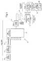
- a delay lock loop 2comprises a voltage controlled oscillator (VCO) 4, constituting a clock means, providing clock pulse signals at an output 6 which clocks a conventional ECL D-type bistable 8, constituting a sampling means, and a known stream cipher pseudo-random sequence generator 10 (PRSG) of conventional design.
- VCOvoltage controlled oscillator
- PRSGknown stream cipher pseudo-random sequence generator 10
- PRBSpseudo-random binary sequence
- the PRBScan be selected via a conventional infra-red key pad (not shown), as used with domestic TV sets and VCR's, and is set to match that of the scrambler used to encode the input data.
- a multiplexed data signal received from a transmitter(as shown in Figure 2) is input to the bistable 8 at its D input 14 which outputs from its Q output 16 a sampled signal sampled at the rate determined by the VCO 4 which provides the clock signals.
- An exclusive -OR (XOR) gate 18compares the sampled signal from the bistable output 16 and the sequence from the PRSG 10 to provide an NRZ video signal at line 20. The output of gate 18 is therefore the generator signal XORed with the sampled signal.
- the presence of videois detected as from a descrambled string of zeros during the line blanking interval using an 8-bit ECL serial to parallel convertor with wired 'OR' outputs as a zero detector 25.
- Pulses from the zero detector 25are coupled via a pulse stretching circuit 26 (the zero detector 25 and the pulse stretching circuit 26 together constituting a signal detector of the present invention) to an integrator 22 which provides at its output 24 an electrical signal representative of the time average of the d.c. component of the output signal of the signal detector, and which constitutes the clock control signal.
- the XOR gate 18, the zero detector 25, the pulse stretching circuit 26 and the integrator 28together constitute a lock means of the present invention.
- the VCO 4is arranged to have a start-up clock rate close but not equal to that of the bit rate of each of the incoming channels. Slippage therefore occurs between the received multiplexed signal and the output from the PRSG 10.
- the XOR gate 18performs a continuous bit by bit comparison of the outputs from the bistable 16 and PRSG 10. When these outputs are the same and in phase, NRZ video is output from the XOR. This is detected by 25, 26 and 22 to provide an output, constituting the clock control signal, which changes the output frequency of the VCO 4 to achieve locking of the clock rate to the channel rate.
- the receiver's PRSG outputwill slip through the channels in the received multiplexed signal until it locks to that channel scrambled by the same sequence as produced by the receiver's PRSG.
- the inputs 12 to the PRSGare arranged to select the characteristic function of the PRSG 10 (and hence the channel to be descrambled) in a known manner.
- the PRSG sequencescan clearly be obtainable by other means, for example reading out sequences stored in permanent or volatile memories, possibly under computer control.
- the descrambled channelcan be obtained via output 20 from the XOR 18 but a preferred arrangement for improved reception is shown in Figure 2 and will now be described.
- a receiver 28incorporates the delay-lock loop 2 of Figure 1 (the same elements being given the same reference numeral) receiving a multiplexed signal from a transmitter 29 via an optical distributor 30 and an optical detector 31.
- a further sampler 34, exclusive 'OR' gate 36 and video decoder 38driven by delayed clock and delay-locked sequence.
- delay-lockoccurs at one edged of the input 'eye' pattern where incoming data transitions provide a suitable reference point.
- the clock signalis delayed by a delay 32 by an interval T/2 to operate the additional sampler 34 at a time corresponding to the instant of optimum signal amplitude.
- This signalis then descrambled by XOR 36 and decoded by the video decoder 38 by conventional means.
- the receiverwas constructed using conventional ECL 100k and ECL III ICs. It could easily be integrated onto a single chip with approximately 300 logic elements, and a 70 MHz maximum clock rate.
- the ECL III bistable set up timeis ⁇ 300 ps, which is sufficient for 2.2 GBit/s transmissions.
- Access to other transparent channelsmay be obtained using further samplers fed via an appropriate clock delay.
- FIG. 3there is shown the 127 - bit stream cipher PRSG 10 configured for use in a transmitter to scramble a channel using standard electronic components which can also be used as the PRSG in the receiver of Figure 1.
- a T.V. communications system 39comprises eight video sources 40, for example a T.V. camera, (only one of which is shown for clarity) each separately encoded by a video encoder 42 and scrambled by a scrambler 44 at the head or transmitter end of a TV communication system.
- the video encoders 42give a serial transmission rate of 70 Mb/s.
- Video encoders giving a serial transmission rate of about 70 Mb/scan be achieved by reducing the composite PAL signal bandwidth to about 5 MHz, sampling at 11.2 MHz and using 6 bit codewords.
- a multiplexer 46contains a clock divider which provides a synchronous clock source for the video encoders 42 and multiplexes the eight scrambled video channels to 2.2 GBd.
- the multiplexed channelsare broadcast by modulating the output of a 1.55 um laser 48, injecting the optical signal into a single mode optical fibre 50 for onward transmission to a 64 way transmissive star 52 in the form of fused biconical taper couplers.
- the transmitter of the applicantencodes each channel prior to multiplexing which is a departure from the hitherto normal line transmission practice which is to use a single line encoder at the output of the multiplexer.
- Disadvantages of such single line encodingare that line encoding after multiplexing (at eight X 70 Mbit/s) is difficult and that the line decoding must be performed in the customers' premises before demultiplexing, both of which are also expensive.
- CMIcoded mark inversion
- Each customer of the 64 possible in this particular embodiment, of which only one is shown for clarity,receives the multiplexed channels at an optical detector 54 whose output is fed to a receiver 28 shown in Figure 2.
- the descrambled signalis then passed to a video decoder 56 whose output drives a television 58.
- a fairly high launch poweris required to provide fan-out to a large number of customers and allow for losses in transmission.
- Semiconductor lasersare available with launch levels of O dBm at 1.3 or 1.5 um into single mode fibre. Fan-out to customers can be provided using fused biconical taper couplers as described in the paper entitled "Wavelength flattened fused couplers" by Mortimore D.B. Electronics Letters 1985 Vol 21 no 17 pp 742-743. These could be a single array in a roadside cabinet or local distribution point, or distributed through the network.
- the suggested power budgetis as follows- launch power 0 dBm fibre loss 5 dB loss of a 64 way power divider 20 dB system margin 4 dB receiver sensitivity -29 dBm
- detector 31can be achieved with a germanium APD, PIN-FET with integrating front end, or a PIN-FET transimpedance receiver.
- a low-cost PIN-bipolar receiverhas been found to provide adequate sensitivity for use with an eight way splitter.
- Figure 5shows a 2.2 Gbit/s multiplex measured on a real time oscilloscope with a transition time of approximately 350 ps. This displays all 32 channels and shows the two active channels with open 'eye' patterns. An 'eye' measured on a sampling oscilloscope had a transition time of ⁇ 75ps. The time to acquire locking increases in proportion to the number of channels multiplexed. This was ⁇ 500ms for the 2.2Gbit/s multiplex.
- FIG. 6illustrates an example of a distribution topology.
- a single fibre 60 from the exchange 62comprising a head end 64 and laser transmitter 66 feeds a number of customers via passive optical splitters at the Cabinet and Distribution Point (DP) positions 68 and 70 respectively.
- Each customer 72receives a fibre 74 (or alternatively coaxial cable) from a DP 70 and, via this, a TDM signal broadcast from the exchange 62.
- the customer's equipmentaccesses the particular channels in the TDM using the delay-lock loop channel selector according to the present invention.
- Up to 32 channelscan be multiplexed to provide service to 32 customers on such a topology within the power budget and speed limitations of existing receivers.
- two DPscan be fed from a single fibre splitter at the cabinet and each customer can be offered a blend of services ranging from his own pre-selectable broad band (68.736 Mbit/s) channel to 32 separate broadcast channels.
- One of the more attractive optionsmight be access to 16 broadcast channels plus up to 16 channels with material pre-selected at the head-end.
- Channelscan be reserved for control, data transfer, and high quality audio services.
- such channelswill not have identifiers such as the line blanking intervals, and may need to be transparent to binary data. Access to a transparent channel is possible using a non-transparent channel as a reference and an additional sampler and clock delay set to offset the required amount to be locked to that channel.
- FIG. 7shows in detail a head-end for transmitting channels for use with the present invention which comprises N analogue video sources 80.
- N analogue video sources 80These are individually coded by video coders 82 by reducing the composite PAL signal bandwidth to about 5 MHz, sampling at 11.2 MHz, and using 6 bit codewords to give a channel rate of 68.736 MHz.
- Each line blanking interval in the video signalis encoded as a string of 128 zeros.
- Each channelis then scrambled by scramblers 84, with its own unique sequence, providing channel identification.
- the channelsare then multiplexed by multiplexer 86 together to give a line rate of Nx68.736 MHz.
- Combinations of silicon and GaAs technologyhave been used to provide 4,8,16 and 32 video channels at 275, 550, 1100 and 2200 MHz, to demonstrate the flexibility of the receiver design.
- the multiplexerdriven at Nx68.736 MHz, provides clock fan-out to each channel at 68.736 MHz.
- the present inventioncan be used as a video demultiplexer and descrambler capable of recovering a designated video channel from a TDM, irrespective of the number of channels presented, up to the limit of the set-up time of the input bistable.
- a broadcast optical networkhas been developed by the applicant over which eight video channels have been broadcast using 1.12 GBd synchronous time division multiplexing (TDM).
- TDMsynchronous time division multiplexing
- a single lasercan serve 64 terminals via passive optical splitters over such a network which if employed with simple demodulation technique should provide low-cost video distribution.
- This techniqueopens up opportunities for a number of new digital video distribution system options.
- a new range of all-digital video receiverscan be envisaged, with channel selection operating in the time domain, in a manner analogous to the conventional frequency domain.
- the receiver specifically described aboverequires a string of logical zeros in the pre-scrambled channel to provide a scrambler sequence in the transmitted signal to which the receiver can phase lock. This occurs in the blanking intervals of pulse code modulated video signals and so the invention is applicable, but not restricted, to use with the video channels. If it is required to send non-video channels which do not have the equivalent of blanking intervals, these may have strings of zeros inserted before scrambling or be accessed as transparent channels as noted above.
- Meansmay be provided for temporarily setting the clock control signal to a value such that the clock in the receiver will be made to slip from the channel to which it is in synchronism. This will start the receiver scanning through the remaining channels.
- the customerhas a receiver with an unalterable PRSG he can still tune into several channels if each is scrambled with a corresponding scrambler sequence as he can start the receiver scanning and it will continue to scan until the clock is brought into synchronism with the next appropriately scrambled signal.
- the level of securityis not high as the descrambling sequence necessarily forms a significant portion of the channel signal to allow channel selection. This will not be a disadvantage for applications where high security is not a requirement.
- the PRSGis preferably a stream cipher sequence generator but other scrambling methods in which the scrambling sequence appears on the scrambled channel to which the receiver can lock its internally generated descrambler sequence can be used.
- the channelhas a signal structure comprising a predetermined sequence as produced by a PRSG or read out of a suitable memory element.
- the receiverhas an additional sampler and a descrambler operating on another time slot via a suitable clock delay.
- This additional descramblercould be of the self synchronising type and could make use of high order prime polynomials.
- Other combined scrambling and encoding schemesare envisaged, to give still higher levels of security eg public key encrypted signals.
- the scrambler sequencewill appear as its complement on the scrambled channel when XOR-ed with it.
- a receiver according to the present invention in which one of the generator signal or the sampled signal to the XOR gate is invertedwill lock to the channel in the manner above described.
- the descrambled signalis then obtainable from a further XOR gate which separately combines the sampled signal with the generator sequence.
- the setting meansmay be controlled by signals sent from the head-end station in one of the channels.
- the received channel signalmay be used directly, or after descrambling in the case that the head-end has performed scrambling.
Landscapes
- Engineering & Computer Science (AREA)
- Computer Networks & Wireless Communication (AREA)
- Signal Processing (AREA)
- Time-Division Multiplex Systems (AREA)
- Optical Communication System (AREA)
- Synchronisation In Digital Transmission Systems (AREA)
Description
- This invention relates to a method of communicating digital signals and a receiver for use with such method particularly, but not exclusively, applicable to the communication of digital video signals via a passive optical network.
- CATV systems have, to date, used analogue transmission schemes because the cost of digital equipment and the bandwidth required for transmission is high but use of digital techniques in television receiver design is increasing with a/d conversion at the input to a single digital processing integrated circuit. Digital encoders are now becoming available which have the potential for low-cost implementation and which provide a picture quality that compares favourably with off-air reception. Among the benefits of digital transmission to users are guaranteed picture quality, the possibility of adding new services to receivers equipped with more advanced digital signal processing, the elimination of the requirement for a/d conversion. Until now the extensive use of digital transmission has been limited by bandwidth and cost constraints of the copper network. However new, low-cost broadcast optical networks are emerging which allow a mixture of services to be provided by time domain or wavelength domain multiplexing (TDM or WDM) on an evolutionary basis. The speed limitation of the electronic components connected to the network rather than the network itself is now the limiting factor on the digital channel capacity per wavelength. Recent papers entitled 'Single mode optical networks' by Payne D. B. and Stern J. R. Proc. Globecom'85 and 'Technical Options for Single Mode Local Loops - TDM or WDM?' by Payne D.B. and Stern J.R. Proceedings of ECOC 1986, Barcelona have discussed the merits of multiple access local networks based upon passive optical networks which use power dividers to serve a large number of customers. These include the possibility of broadband transmission on a single carrier and upgrading via wave division multiplexing (WDM). Whilst WDM would provide one solution to this problem, TDM seems more attractive because only a single transmitter is required.
- The passive, multiple-access architecture has a number of operational advantages as discussed in the paper on single mode optical networks referenced above. The need for cables with a large number of fibres near the head end is reduced, it is more reliable and easier to maintain than a network with active switching at splitting nodes, and it is possible to upgrade the network as wavelength multiplexing components become available. These networks are most cost sensitive in the customers' final drop and equipment as the cost of the head-end is shared by all users. An objective of the present invention is to provide a method and a receiver for use with such a method whereby customers can access a large number of digital TV channels in a way which can reduce the cost of customer equipment by eliminating the need for digital circuitry operating at the multiplex rate.
- US patent No. 3,649,915 (Mildonian) discloses scrambling a plurality of digital video signals, multiplexing the scrambled signals, converting the multiplexed signal to a multilevel signal and transmitting the multilevel signal via a microwave radio relay transmission facility. The digital signals are recovered in receivers by an inverse process in which a demultiplexer must operate at the bit-rate of the transmitted multiplexed signal. Another object of the present invention is to provide a method of signal communication and a receiver in which the received signal is processed at the channel bit-rate, thereby avoiding the use of a demultiplexer operating at the transmission bit-rate.
- Mildonian employs scrambling to eliminate essentially the unwanted DC component in the internally generated multilevel signal, and uses the same scrambling sequence for each digital signal. Thus, after demultiplexing the received signal, all the channels are descrambled to produce digital signals from which the original analogue forms are derived.
- It is a further object of the present invention to provide a method of signal communication and a receiver in which a level of security can be given to some or all of the multiplexed channels by scrambling prior to transmission and in which the channel selection and descrambling is carried out automatically by the receiver.
- According to one aspect of the present invention there is provided a receiver receiving a time division multiplexed signal comprising two or more time division multiplexed channels of digital signals at a predetermined bit-rate and for selectively extracting a signal constituting one of the two or more time division multiplexed channels of digital signals, the signal constituting said one channel having been scrambled before forming the multiplexed signal using a predetermined digital sequence, which receiver comprises a clock means arranged to provide clock pulses having a clock pulse repetition rate dependent on a clock control signal, and initially nearly equal to said predetermined channel bit-rate and a digital sequence generator means for providing a generator signal representative of the predetermined digital sequence at the clock pulse repetition rate, and is characterised by;
a first sampling means arranged to provide a sampled signal which is the received multiplexed signal sampled at the clock pulse repetition rate; and
and lock means arranged to perform a descrambling process on the sampled signal in accordance with the generator signal and provide an output signal, to detect in the output signal the presence of the known characteristic, and to control the clock pulse repetition rate in dependence upon the detection of the known characteristic whereby, in use, the clock pulse repetition rate is synchronised to said one time division multiplexed channel. - The scrambling and descrambling is preferably by XOR-ing with the scrambling and descrambling sequences as this tends to produce a balanced data signal. The lock means, preferably in the form of a delay-lock loop, is arranged such that when there is no correlation between the sampled and generator signal the clock control signal produced causes the clock pulse repetition rate to be slightly different from (it can be above or below) the channel bit rate. There will therefore be slip between the received multiplexed channel signal and the generator signal. When the scrambled channel signal becomes aligned with the descrambling sequence, a descrambled video channel is output. Additional circuitry is required to detect the presence of this video channel, so that the delay-lock loop may be closed. One method of achieving this is as follows.
- The video channel contains long strings of zeros in the line blanking intervals, and these are detected using an 8-bit ECL serial/parallel converter with wired 'or' outputs. This produces a logical 'O' output during the line blanking interval if the channel was scrambled prior to transmission by a sequence corresponding to the receiver's descrambling sequence. The descrambled signal is fed to a circuit designed to lengthen the zero level pulses. The change in signal level which occurs when this string of descrambled zeros is detected is integrated, altering the frequency of the VCO to give delay-lock at the incoming channel rate.
- The lock means may comprise a comparison means providing an output signal representative of the generator signal XORed with the sampled signal, a signal detector coupled to receive the output signal of the comparison means, and being arranged to provide an output having a d.c. component, and an averaging means arranged to provide the clock control signal such that the clock control signal is representative of the time - average of the d.c. component of the output of the signal detector. It will be clear that the above invention can be operated with logical 1s as well as logical Os as the line blanking signal by the inclusion of inverters in the appropriate places.
- Delay-lock occurs at the edge of the appropriate channel 'eye' pattern in the multiplex, where incoming data transitions provide a suitable reference point so the descrambled data in the delay-lock loop therefore is prone to errors. To achieve error-free operation of the video channel, it is preferred that the input data is also sampled by a second D-type bistable, clocked at the centre of the 'eye' pattern via a T/2 clock delay line. This data is then descrambled independently using the locally generated PRBS.
- Using this method of communication the receiver will automatically select a channel which has been scrambled by the same sequence as generated by the sequence generator in the receiver and at the same time automatically adjust the clock pulse repetition rate relative to that channel thereby obviating the need for a clock recovery system independent of the descrambler.
- The demultiplexer selects a single channel using a sampler clocked at a rate equal to the channel rate and locked to it by the delay-lock loop. A benefit of this method of demultiplexing is that clock recovery and time slot synchronisation is achieved at the baseband rate enabling all the receiver electronics to operate at the channel rate. A further benefit is that the same channel selection technique operates independently of the number of channels up to the speed limitation of the sampler.
- Conveniently, the digital sequence is provided by a dedicated pseudo - random sequence generator although alternative methods can be employed for example reading out a sequence stored in an EPROM or generating the sequence by a general purpose computer.
- Preferably the pseudo-random sequence generator is a stream cipher.
- According to another aspect of the present invention a method of communication comprising transmitting a time division multiplexed signal comprising two or more time division multiplexed channels of digital signals scrambling prior to transmission the signal constituting at least one of the channels using a predetermined digital sequence receiving the transmitted time division multiplexed signal, sampling the received multiplexed signal at a controllable clock pulse repetition rate to provide a sampled signal, generating at the clock pulse repetition rate a descrambling signal representative of the predetermined digital sequence, performing a descrambling process on the sampled signal in accordance with the descrambling signal to produce an output signal, controlling the clock pulse repetition rate in dependence upon the detection of the known characteristic to synchronise the clock pulse repetition rate to said one time division multiplexed channel, and providing a descrambled signal.
- Preferably at least one other of the signals constituting channels in the multiplexed signal is scrambled using a respective predetermined digital sequence, the predetermined digital sequences being different from one another, and the resulting time division multiplexed signal is transmitted to one or more receivers.
- Various service protocols between the transmitter and the receivers to which the multiplexed channels are transmitted can be set up. In one arrangement the receiver is provided with means whereby the customer can alter the sequence generated by the sequence generator. This can be readily achieved by providing a pseudo-random sequence generator (PRSG) whose output is determined by a characteristic function which can be set by, for example switches, in known manner. The customer can then select one or more of the channels to be received by setting the characteristic function to that of the desired channel. By providing the customer with the means to set only a subset of the characteristic functions of the channels at his receiver he will be able to select a channel from that subset of channels only. The provider of the signals to the customer can alter the availability of channels to such a customer by choosing which channels are scrambled with the sequences available to a particular customer. Each customer may have a fixed, unalterable set of available characteristic functions distinct from another customer yet they can receive the same data if the data is separately scrambled onto two separate channels using two different scrambling sequences.
- Embodiments of receivers and a method of communication according to the present invention will now be described, by way of example only, with reference to the accompanying drawings, in which -
- Figure 1 is a schematic diagram of a delay-lock loop for use in a receiver of the present invention;
- Figure 2 is a schematic diagram of a distribution arrangement and includes a block diagram of a receiver according to the present invention;
- Figure 3 is a circuit diagram of a PRSG scrambler suitable for use with the present invention;
- Figure 4 is a block diagram of a TV communication system using the receiver of Figure 2;
- Figure 5 shows part of a 2.2 Gbit/s multiplexed signal;
- Figure 6 shows an exemplary distribution topography; and
- Figure 7 is a schematic diagram of a head-end.
- Referring to Figure 1, a
delay lock loop 2 comprises a voltage controlled oscillator (VCO) 4, constituting a clock means, providing clock pulse signals at anoutput 6 which clocks a conventional ECL D-type bistable 8, constituting a sampling means, and a known stream cipher pseudo-random sequence generator 10 (PRSG) of conventional design. The pseudo-random binary sequence (PRBS) output from the PRSG constitutes a generator signal of the present invention and is dependent on a predetermined characteristic function represented by the switch inputs 12 (constituting a setting means of the present invention) to PRSG 10. The PRBS can be selected via a conventional infra-red key pad (not shown), as used with domestic TV sets and VCR's, and is set to match that of the scrambler used to encode the input data. A multiplexed data signal received from a transmitter (as shown in Figure 2) is input to the bistable 8 at itsD input 14 which outputs from its Q output 16 a sampled signal sampled at the rate determined by theVCO 4 which provides the clock signals. An exclusive -OR (XOR)gate 18 compares the sampled signal from thebistable output 16 and the sequence from thePRSG 10 to provide an NRZ video signal atline 20. The output ofgate 18 is therefore the generator signal XORed with the sampled signal. The presence of video is detected as from a descrambled string of zeros during the line blanking interval using an 8-bit ECL serial to parallel convertor with wired 'OR' outputs as a zerodetector 25. Pulses from the zerodetector 25 are coupled via a pulse stretching circuit 26 (the zerodetector 25 and thepulse stretching circuit 26 together constituting a signal detector of the present invention) to anintegrator 22 which provides at itsoutput 24 an electrical signal representative of the time average of the d.c. component of the output signal of the signal detector, and which constitutes the clock control signal. TheXOR gate 18, the zerodetector 25, thepulse stretching circuit 26 and theintegrator 28 together constitute a lock means of the present invention. - The
VCO 4 is arranged to have a start-up clock rate close but not equal to that of the bit rate of each of the incoming channels. Slippage therefore occurs between the received multiplexed signal and the output from thePRSG 10. TheXOR gate 18 performs a continuous bit by bit comparison of the outputs from the bistable 16 andPRSG 10. When these outputs are the same and in phase, NRZ video is output from the XOR. This is detected by 25, 26 and 22 to provide an output, constituting the clock control signal, which changes the output frequency of theVCO 4 to achieve locking of the clock rate to the channel rate. - The receiver's PRSG output will slip through the channels in the received multiplexed signal until it locks to that channel scrambled by the same sequence as produced by the receiver's PRSG.
- The
inputs 12 to the PRSG are arranged to select the characteristic function of the PRSG 10 (and hence the channel to be descrambled) in a known manner. The PRSG sequences can clearly be obtainable by other means, for example reading out sequences stored in permanent or volatile memories, possibly under computer control. The descrambled channel can be obtained viaoutput 20 from theXOR 18 but a preferred arrangement for improved reception is shown in Figure 2 and will now be described. - Referring to Figure 2, a
receiver 28 incorporates the delay-lock loop 2 of Figure 1 (the same elements being given the same reference numeral) receiving a multiplexed signal from atransmitter 29 via anoptical distributor 30 and anoptical detector 31. There is included afurther sampler 34, exclusive 'OR'gate 36 andvideo decoder 38 driven by delayed clock and delay-locked sequence. In normal operations, delay-lock occurs at one edged of the input 'eye' pattern where incoming data transitions provide a suitable reference point. To obtain low error rates, the clock signal is delayed by adelay 32 by an interval T/2 to operate theadditional sampler 34 at a time corresponding to the instant of optimum signal amplitude. This signal is then descrambled byXOR 36 and decoded by thevideo decoder 38 by conventional means. - The receiver was constructed using conventional ECL 100k and ECL III ICs. It could easily be integrated onto a single chip with approximately 300 logic elements, and a 70 MHz maximum clock rate. The ECL III bistable set up time is <300 ps, which is sufficient for 2.2 GBit/s transmissions.
- Access to other transparent channels may be obtained using further samplers fed via an appropriate clock delay.
- Referring now to Figure 3, there is shown the 127 - bit
stream cipher PRSG 10 configured for use in a transmitter to scramble a channel using standard electronic components which can also be used as the PRSG in the receiver of Figure 1. - Referring now to Fig 4 a T.V. communications system 39 comprises eight
video sources 40, for example a T.V. camera, (only one of which is shown for clarity) each separately encoded by avideo encoder 42 and scrambled by ascrambler 44 at the head or transmitter end of a TV communication system. Thevideo encoders 42 give a serial transmission rate of 70 Mb/s. Video encoders giving a serial transmission rate of about 70 Mb/s can be achieved by reducing the composite PAL signal bandwidth to about 5 MHz, sampling at 11.2 MHz and using 6 bit codewords. Amultiplexer 46 contains a clock divider which provides a synchronous clock source for thevideo encoders 42 and multiplexes the eight scrambled video channels to 2.2 GBd. The multiplexed channels are broadcast by modulating the output of a 1.55 umlaser 48, injecting the optical signal into a single modeoptical fibre 50 for onward transmission to a 64way transmissive star 52 in the form of fused biconical taper couplers. - The transmitter of the applicant encodes each channel prior to multiplexing which is a departure from the hitherto normal line transmission practice which is to use a single line encoder at the output of the multiplexer. Disadvantages of such single line encoding are that line encoding after multiplexing (at eight
X 70 Mbit/s) is difficult and that the line decoding must be performed in the customers' premises before demultiplexing, both of which are also expensive. - One line code scheme that may be used is the known coded mark inversion (CMI). This is a biphase code which is simple and cheap to implement. One disadvantage of CMI is that it doubles the transmission rate but on the other hand the composite 1.12 GBd signal has the desirable properties of being both balanced and having a constrained maximum run length of 24 like elements.
- Each customer of the 64 possible in this particular embodiment, of which only one is shown for clarity, receives the multiplexed channels at an
optical detector 54 whose output is fed to areceiver 28 shown in Figure 2. The descrambled signal is then passed to avideo decoder 56 whose output drives atelevision 58. - A fairly high launch power is required to provide fan-out to a large number of customers and allow for losses in transmission. Semiconductor lasers are available with launch levels of O dBm at 1.3 or 1.5 um into single mode fibre. Fan-out to customers can be provided using fused biconical taper couplers as described in the paper entitled "Wavelength flattened fused couplers" by Mortimore D.B. Electronics Letters 1985 Vol 21 no 17 pp 742-743. These could be a single array in a roadside cabinet or local distribution point, or distributed through the network. The suggested power budget is as follows-
launch power 0 dBm fibre loss 5 dB loss of a 64 way power divider 20 dB system margin 4 dB receiver sensitivity -29 dBm - The required sensitivity of
detector 31 can be achieved with a germanium APD, PIN-FET with integrating front end, or a PIN-FET transimpedance receiver. A low-cost PIN-bipolar receiver has been found to provide adequate sensitivity for use with an eight way splitter. - Figure 5 shows a 2.2 Gbit/s multiplex measured on a real time oscilloscope with a transition time of approximately 350 ps. This displays all 32 channels and shows the two active channels with open 'eye' patterns. An 'eye' measured on a sampling oscilloscope had a transition time of <75ps. The time to acquire locking increases in proportion to the number of channels multiplexed. This was <500ms for the 2.2Gbit/s multiplex.
- Figure 6 illustrates an example of a distribution topology. A
single fibre 60 from theexchange 62 comprising ahead end 64 andlaser transmitter 66 feeds a number of customers via passive optical splitters at the Cabinet and Distribution Point (DP) positions 68 and 70 respectively. Eachcustomer 72 receives a fibre 74 (or alternatively coaxial cable) from aDP 70 and, via this, a TDM signal broadcast from theexchange 62. The customer's equipment accesses the particular channels in the TDM using the delay-lock loop channel selector according to the present invention. - Up to 32 channels can be multiplexed to provide service to 32 customers on such a topology within the power budget and speed limitations of existing receivers. Thus two DPs can be fed from a single fibre splitter at the cabinet and each customer can be offered a blend of services ranging from his own pre-selectable broad band (68.736 Mbit/s) channel to 32 separate broadcast channels. One of the more attractive options might be access to 16 broadcast channels plus up to 16 channels with material pre-selected at the head-end. Channels can be reserved for control, data transfer, and high quality audio services. In general, such channels will not have identifiers such as the line blanking intervals, and may need to be transparent to binary data. Access to a transparent channel is possible using a non-transparent channel as a reference and an additional sampler and clock delay set to offset the required amount to be locked to that channel.
- Casual access to channels can be prevented by the design of the descramblers in customers' equipment which access time slots using unique descrambling sequences. To ensure that customers only descramble authorised channels it would be necessary for operating companies to maintain control of the key polynomials.
- Figure 7 shows in detail a head-end for transmitting channels for use with the present invention which comprises N analogue video sources 80. These are individually coded by
video coders 82 by reducing the composite PAL signal bandwidth to about 5 MHz, sampling at 11.2 MHz, and using 6 bit codewords to give a channel rate of 68.736 MHz. Each line blanking interval in the video signal is encoded as a string of 128 zeros. Each channel is then scrambled byscramblers 84, with its own unique sequence, providing channel identification. The channels are then multiplexed bymultiplexer 86 together to give a line rate of Nx68.736 MHz. Combinations of silicon and GaAs technology have been used to provide 4,8,16 and 32 video channels at 275, 550, 1100 and 2200 MHz, to demonstrate the flexibility of the receiver design. The multiplexer, driven at Nx68.736 MHz, provides clock fan-out to each channel at 68.736 MHz. - The present invention can be used as a video demultiplexer and descrambler capable of recovering a designated video channel from a TDM, irrespective of the number of channels presented, up to the limit of the set-up time of the input bistable.
- A broadcast optical network has been developed by the applicant over which eight video channels have been broadcast using 1.12 GBd synchronous time division multiplexing (TDM). A single laser can serve 64 terminals via passive optical splitters over such a network which if employed with simple demodulation technique should provide low-cost video distribution. This technique opens up opportunities for a number of new digital video distribution system options. A new range of all-digital video receivers can be envisaged, with channel selection operating in the time domain, in a manner analogous to the conventional frequency domain.
- The receiver specifically described above requires a string of logical zeros in the pre-scrambled channel to provide a scrambler sequence in the transmitted signal to which the receiver can phase lock. This occurs in the blanking intervals of pulse code modulated video signals and so the invention is applicable, but not restricted, to use with the video channels. If it is required to send non-video channels which do not have the equivalent of blanking intervals, these may have strings of zeros inserted before scrambling or be accessed as transparent channels as noted above.
- Means may be provided for temporarily setting the clock control signal to a value such that the clock in the receiver will be made to slip from the channel to which it is in synchronism. This will start the receiver scanning through the remaining channels. Thus if the customer has a receiver with an unalterable PRSG he can still tune into several channels if each is scrambled with a corresponding scrambler sequence as he can start the receiver scanning and it will continue to scan until the clock is brought into synchronism with the next appropriately scrambled signal.
- It will be appreciated that the level of security is not high as the descrambling sequence necessarily forms a significant portion of the channel signal to allow channel selection. This will not be a disadvantage for applications where high security is not a requirement.
- The PRSG is preferably a stream cipher sequence generator but other scrambling methods in which the scrambling sequence appears on the scrambled channel to which the receiver can lock its internally generated descrambler sequence can be used.
- In another arrangement of receiver according to the present invention in which higher security is obtained the channel has a signal structure comprising a predetermined sequence as produced by a PRSG or read out of a suitable memory element. In such a system the receiver has an additional sampler and a descrambler operating on another time slot via a suitable clock delay. This additional descrambler could be of the self synchronising type and could make use of high order prime polynomials. Other combined scrambling and encoding schemes are envisaged, to give still higher levels of security eg public key encrypted signals.
- If the channel to be scrambled has large components of strings of binary '1's, the scrambler sequence will appear as its complement on the scrambled channel when XOR-ed with it. A receiver according to the present invention in which one of the generator signal or the sampled signal to the XOR gate is inverted will lock to the channel in the manner above described. The descrambled signal is then obtainable from a further XOR gate which separately combines the sampled signal with the generator sequence.
- In addition to the setting means being under the control of an operator of the receiver, the setting means may be controlled by signals sent from the head-end station in one of the channels. The received channel signal may be used directly, or after descrambling in the case that the head-end has performed scrambling.
Claims (16)
- A receiver (28) for receiving a time division multiplexed signal comprising two or more time division multiplexed channels of digital signals at a predetermined channel bit-rate and for selectively extracting a signal constituting one of the two or more time division multiplexed channels of digital signals, the signal constituting said one channel having been scrambled before forming the multiplexed signal using a predetermined digital sequence, which receiver comprises a clock means (4) arranged to provide clock pulses having a clock pulse repetition rate dependent on a clock control signal, and initially nearly equal to said predetermined channel bit-rate, and a digital sequence generator means (10) for providing a generator signal representative of the predetermined digital sequence at the clock pulse repetition rate, and is characterised by;
a first sampling means (8) arranged to provide a sampled signal which is the received multiplexed signal sampled at the clock pulse repetition rate; and
and lock means (18, 22, 25, 26) arranged to perform a descrambling process on the sampled signal in accordance with the generator signal and provide an output signal, to detect in the output signal the presence of the known characteristic, and to control the clock pulse repetition rate in dependence upon the detection of the known characteristic whereby, in use, the clock pulse repetition rate is synchronised to said one time division multiplexed channel. - A receiver as claimed in claim 1, in which the lock means comprises a comparison means (18) providing an output signal representative of the generator signal XORed with the sampled signal, a signal detector (25,26) coupled to receive the output signal of the comparison means and being arranged to provide an output having a d.c. component, and an averaging means (22) arranged to provide the clock control signal such that the clock control signal is representative of the time-average of the d.c. component of the output of the signal detector (25, 26).
- A receiver as claimed in claim 2, in which the signal detector (25, 26) comprises a logical zero detector (25).
- A receiver as claimed in any one of the preceding claims, in which the lock means (25, 26) is arranged to lock to the line blanking interval of a video channel.
- A receiver as claimed in any one of the preceding claims, including a second sampling means (32, 34) arranged to provide a sample signal which is the received multiplexed signal sampled at the clock pulse repetition rate at times delayed with respect to the first sampling means.
- A receiver as claimed in any one of the preceding claims, in which the digital sequence is provided by a pseudo-random sequence generator (10).
- A receiver as claimed in claim 6, including a setting means (12) whereby the characteristic function of the pseudo-random sequence generator (10) can be set by an operator of the receiver.
- A receiver as claimed in claim 7, in which the setting means (12) is controlled by the received multiplexed signal before or after descrambling.
- A receiver as claimed in any one of the preceding claims, and further comprising a self synchronising descrambler.
- A receiver as claimed in any one of the preceding claims, including means (not shown) for deactivating the lock means thereby causing the generator signal output to slip relative to the received multiplexed signal.
- A receiver as claimed in any one of the preceding claims, including a transparent channel sampler driven by a further clock signal which is time delayed from the clock pulses from the clock means.
- A method of communication comprising transmitting a time division multiplexed signal comprising two or more time division multiplexed channels of digital signals, scrambling prior to transmission the signal constituting at least one of the channels using a predetermined digital sequence, receiving the transmitted time division multiplexed signal, and characterised by sampling the received multiplexed signal at a controllable clock pulse repetition rate (6) to provide a sampled signal (16), generating (10) at the clock pulse repetition rate a descrambling signal representative of the predetermined digital sequence, performing a descrambling process (18, 36) on the sampled signal in accordance with the descrambling signal to produce an output signal (20), detecting (25) a known characteristic of the output signal, controlling (22, 24, 26) the clock pulse repetition rate in dependence upon the detection of the known characteristic to synchronise the clock pulse repetition rate to said one time division multiplexed channel, and providing a descrambled signal (20).
- A method as claimed in claim 12, in which the output signal constitutes the provided descrambled signal.
- A method as claimed in claim 12, in which the descrambled signal is provided by further sampling the received multiplexed signal at times which are delayed with respect to the clock pulses to produce a further sampled signal, and performing a descrambling process on the further sampled signal in accordance with a further scrambling signal which is the descrambling signal correspondingly delayed.
- A method as claimed in claim 14, in which the delay of the further sampling times is substantially equal to half the period of the clock pulse repetition rate.
- A method as claimed in any one of claims 12 to 15, in which at least one other of the signals constituting channels in the multiplexed signal is scrambled using a respective predetermined digital sequence, the predetermined digital sequences being different from one another, and the resulting time division multiplexed signal is transmitted to one or more receivers.
Priority Applications (1)
| Application Number | Priority Date | Filing Date | Title |
|---|---|---|---|
| AT88308382TATE91364T1 (en) | 1987-09-14 | 1988-09-09 | METHOD OF DIGITAL SIGNAL TRANSMISSION AND RECEIVER TO CARRY OUT THE METHOD. |
Applications Claiming Priority (4)
| Application Number | Priority Date | Filing Date | Title |
|---|---|---|---|
| GB8721603 | 1987-09-14 | ||
| GB878721603AGB8721603D0 (en) | 1987-09-14 | 1987-09-14 | Communicating digital signals |
| GB888804552AGB8804552D0 (en) | 1988-02-26 | 1988-02-26 | Method of communicating digital signals & receiver for use with such method |
| GB8804552 | 1988-02-26 |
Publications (2)
| Publication Number | Publication Date |
|---|---|
| EP0308150A1 EP0308150A1 (en) | 1989-03-22 |
| EP0308150B1true EP0308150B1 (en) | 1993-07-07 |
Family
ID=26292735
Family Applications (1)
| Application Number | Title | Priority Date | Filing Date |
|---|---|---|---|
| EP88308382AExpired - LifetimeEP0308150B1 (en) | 1987-09-14 | 1988-09-09 | Method of communicating digital signals and receiver for use with such method |
Country Status (8)
| Country | Link |
|---|---|
| US (1) | US5144669A (en) |
| EP (1) | EP0308150B1 (en) |
| JP (1) | JP2807244B2 (en) |
| CA (1) | CA1325296C (en) |
| DE (1) | DE3882185T2 (en) |
| ES (1) | ES2041315T3 (en) |
| HK (1) | HK130596A (en) |
| WO (1) | WO1989002681A1 (en) |
Cited By (3)
| Publication number | Priority date | Publication date | Assignee | Title |
|---|---|---|---|---|
| US7310522B2 (en) | 1996-05-20 | 2007-12-18 | Adc Telecommunications, Inc. | Systems for synchronous multipoint-to-point orthogonal frequency division multiplexing communication |
| USRE41771E1 (en) | 1995-02-06 | 2010-09-28 | Adc Telecommunications, Inc. | System for multiple use subchannels |
| USRE42236E1 (en) | 1995-02-06 | 2011-03-22 | Adc Telecommunications, Inc. | Multiuse subcarriers in multipoint-to-point communication using orthogonal frequency division multiplexing |
Families Citing this family (22)
| Publication number | Priority date | Publication date | Assignee | Title |
|---|---|---|---|---|
| US5519830A (en)* | 1993-06-10 | 1996-05-21 | Adc Telecommunications, Inc. | Point-to-multipoint performance monitoring and failure isolation system |
| US5408462A (en)* | 1993-10-07 | 1995-04-18 | Adc Telecommunications, Inc. | Protection switching apparatus and method |
| US5453737A (en)* | 1993-10-08 | 1995-09-26 | Adc Telecommunications, Inc. | Control and communications apparatus |
| US5574673A (en)* | 1993-11-29 | 1996-11-12 | Board Of Regents, The University Of Texas System | Parallel architecture for generating pseudo-random sequences |
| FR2719175B1 (en)* | 1994-04-20 | 1996-05-31 | Cit Alcatel | Optical transmission method having reduced sensitivity to dispersion, and transmission system for implementing this method. |
| FI97184C (en)* | 1994-11-07 | 1996-10-25 | Nokia Telecommunications Oy | Method and apparatus for realizing a subscriber-specific scrambling and descrambling in a subscriber network |
| US7224798B2 (en)* | 1995-04-03 | 2007-05-29 | Scientific-Atlanta, Inc. | Methods and apparatus for providing a partial dual-encrypted stream in a conditional access overlay system |
| US5786919A (en)* | 1996-09-05 | 1998-07-28 | The United States Of America As Represented By The Secretary Of The Navy | Data multiplexing node for line array |
| US6243372B1 (en)* | 1996-11-14 | 2001-06-05 | Omnipoint Corporation | Methods and apparatus for synchronization in a wireless network |
| US6044122A (en)* | 1997-01-23 | 2000-03-28 | Ericsson, Inc. | Digital phase acquisition with delay locked loop |
| DE69833821T2 (en)* | 1997-09-18 | 2006-11-30 | Matsushita Electric Industrial Co., Ltd., Kadoma | Transmission method and apparatus for combined multiplexing and encrypting |
| US6088414A (en)* | 1997-12-18 | 2000-07-11 | Alcatel Usa Sourcing, L.P. | Method of frequency and phase locking in a plurality of temporal frames |
| US6118836A (en)* | 1997-12-18 | 2000-09-12 | Alcatel Usa Sourcing L.P. | Frequency and phase locking apparatus |
| US6577732B1 (en)* | 1998-09-22 | 2003-06-10 | Lucent Technologies Inc. | Hierarchical encryption technique for dense wavelength division multiplexed systems using a wavelength bus architecture |
| US6973188B1 (en)* | 2002-02-25 | 2005-12-06 | Lockheed Martin Corporation | Analog scrambler |
| US7277637B2 (en)* | 2003-01-03 | 2007-10-02 | Tellabs Bedford, Inc. | Fiber to the home broadband home unit |
| BRPI0413851B1 (en)* | 2003-08-29 | 2018-04-24 | The Directv Group, Inc. | "Method of scrambling signal and scrambling symbols in a data transmission system and apparatus for scrambling symbols in a data transmission system" |
| KR100520656B1 (en)* | 2003-09-26 | 2005-10-13 | 삼성전자주식회사 | Ethernet Passive Optical Network for Convergence of Broadcasting and Telecommunication Being Capable of Broadcast/Image Security |
| US20060023874A1 (en)* | 2004-07-29 | 2006-02-02 | International Business Machines Corporation | Method and multiline scrambled clock architecture with random state selection for implementing lower electromagnetic emissions |
| JP4804735B2 (en)* | 2004-09-30 | 2011-11-02 | 富士通株式会社 | Optical transmission system and optical transmission method |
| US7696797B1 (en)* | 2005-03-31 | 2010-04-13 | Schnaitter William N | Signal generator with output frequency greater than the oscillator frequency |
| EP2262178A1 (en)* | 2009-06-10 | 2010-12-15 | Alcatel Lucent | Method for discontinuously transferring data in a point-to-multipoint access network, central unit, and network termination unit |
Family Cites Families (12)
| Publication number | Priority date | Publication date | Assignee | Title |
|---|---|---|---|---|
| BE646982A (en)* | 1963-04-23 | |||
| NL6702874A (en)* | 1966-08-27 | 1968-08-26 | ||
| CA925212A (en)* | 1970-06-22 | 1973-04-24 | Western Electric Company, Incorporated | Digital data scrambler-descrambler apparatus for improved error performance |
| US3950616A (en)* | 1975-04-08 | 1976-04-13 | Bell Telephone Laboratories, Incorporated | Alignment of bytes in a digital data bit stream |
| US4052565A (en)* | 1975-05-28 | 1977-10-04 | Martin Marietta Corporation | Walsh function signal scrambler |
| US4221931A (en)* | 1977-10-17 | 1980-09-09 | Harris Corporation | Time division multiplied speech scrambler |
| JPS5539444A (en)* | 1978-09-13 | 1980-03-19 | Pioneer Electronic Corp | Scramble/descramble system for catv broadcast |
| US4221005A (en)* | 1979-05-21 | 1980-09-02 | Nasa | Pseudonoise code tracking loop |
| DE3010969A1 (en)* | 1980-03-21 | 1981-10-01 | Siemens AG, 1000 Berlin und 8000 München | PCM SYSTEM WITH TRANSMITTER ENCODER AND RECEIVED DESIGNER |
| GB2140656A (en)* | 1983-05-13 | 1984-11-28 | Philips Electronic Associated | Television transmission system |
| JPH0654973B2 (en)* | 1983-11-09 | 1994-07-20 | ソニー株式会社 | Digital signal transmission device using CATV line |
| US4866773A (en)* | 1988-05-20 | 1989-09-12 | Dan Lubarsky | System for interfacing a digital encryption device to a time-division multiplexed communication system |
- 1988
- 1988-09-09DEDE88308382Tpatent/DE3882185T2/ennot_activeExpired - Fee Related
- 1988-09-09WOPCT/GB1988/000744patent/WO1989002681A1/enunknown
- 1988-09-09JPJP63507245Apatent/JP2807244B2/ennot_activeExpired - Fee Related
- 1988-09-09EPEP88308382Apatent/EP0308150B1/ennot_activeExpired - Lifetime
- 1988-09-09ESES198888308382Tpatent/ES2041315T3/ennot_activeExpired - Lifetime
- 1988-09-09USUS07/348,575patent/US5144669A/ennot_activeExpired - Fee Related
- 1988-09-13CACA000577282Apatent/CA1325296C/ennot_activeExpired - Fee Related
- 1996
- 1996-07-18HKHK130596Apatent/HK130596A/ennot_activeIP Right Cessation
Cited By (27)
| Publication number | Priority date | Publication date | Assignee | Title |
|---|---|---|---|---|
| USRE44460E1 (en) | 1994-09-26 | 2013-08-27 | Htc Corporation | Systems for synchronous multipoint-to-point orthogonal frequency division multiplexing communication |
| US7912138B2 (en) | 1995-02-06 | 2011-03-22 | Adc Telecommunications, Inc. | Timing and symbol alignment in multipoint-to-point communication using orthogonal frequency division multiplexing |
| US8315150B2 (en) | 1995-02-06 | 2012-11-20 | Htc Corporation | Synchronized multipoint-to-point communication using orthogonal frequency division |
| US7675843B2 (en) | 1995-02-06 | 2010-03-09 | Adc Telecommunications, Inc. | Multipoint-to-point communication using orthogonal frequency division multiplexing |
| US7697453B2 (en) | 1995-02-06 | 2010-04-13 | Adc Telecommunications, Inc. | Synchronization techniques in multipoint-to-point communication using orthogonal frequency division multiplexing |
| US7706349B2 (en) | 1995-02-06 | 2010-04-27 | Adc Telecommunications, Inc. | Methods and systems for selecting modulation in an orthogonal frequency division multiplexing system |
| US7756060B2 (en) | 1995-02-06 | 2010-07-13 | Adc Telecommunications, Inc. | Tone allocation in multipoint-to-point communication using orthogonal frequency division multiplexing |
| US7773537B2 (en) | 1995-02-06 | 2010-08-10 | Adc Telecommunications, Inc. | Ranging and round trip delay timing adjustment in a multi-point to point bidirectional communication system |
| USRE41771E1 (en) | 1995-02-06 | 2010-09-28 | Adc Telecommunications, Inc. | System for multiple use subchannels |
| US7872985B2 (en) | 1995-02-06 | 2011-01-18 | Adc Dsl Systems, Inc. | System for multi-frame alignment |
| US7881181B2 (en) | 1995-02-06 | 2011-02-01 | Adc Telecommunications, Inc. | Systems and method for orthogonal frequency divisional multiplexing |
| US7881180B2 (en) | 1995-02-06 | 2011-02-01 | Adc Telecommunications, Inc. | Systems and method for orthogonal frequency divisional multiplexing |
| US7535822B2 (en) | 1995-02-06 | 2009-05-19 | Adc Telecommunications, Inc. | Synchronization of remote units for a communication network |
| US7672219B2 (en) | 1995-02-06 | 2010-03-02 | Adc Telecommunications, Inc. | Multipoint-to-point communication using orthogonal frequency division multiplexing |
| USRE42236E1 (en) | 1995-02-06 | 2011-03-22 | Adc Telecommunications, Inc. | Multiuse subcarriers in multipoint-to-point communication using orthogonal frequency division multiplexing |
| US8174956B2 (en) | 1995-02-06 | 2012-05-08 | Htc Corporation | Systems and method for orthogonal frequency divisional multiplexing |
| US7983141B2 (en) | 1995-02-06 | 2011-07-19 | Geile Michael J | Synchronized multipoint-to-point communication using orthogonal frequency division |
| US7995454B2 (en) | 1995-02-06 | 2011-08-09 | Htc Corporation | Systems and method for orthogonal frequency divisional multiplexing |
| US8089853B2 (en) | 1995-02-06 | 2012-01-03 | Htc Corporation | Systems and method for orthogonal frequency divisional multiplexing |
| US7957265B2 (en) | 1995-02-06 | 2011-06-07 | Adc Telecommunications, Inc. | Systems and method for orthogonal frequency divisional multiplexing |
| US8199632B2 (en) | 1995-02-06 | 2012-06-12 | Htc Corporation | Systems and method for orthogonal frequency divisional multiplexing |
| US8213398B2 (en) | 1995-02-06 | 2012-07-03 | Htc Corporation | Method for multiple use subchannels |
| US8213399B2 (en) | 1995-02-06 | 2012-07-03 | Htc Corporation | System for multiple use subchannels |
| US7936662B2 (en) | 1995-02-06 | 2011-05-03 | Adc Telecommunications, Inc. | Ranging and round trip delay timing adjustment in a multi-point to point bidirectional communication system |
| US8351321B2 (en) | 1995-02-06 | 2013-01-08 | Htc Corporation | Systems and method for orthogonal frequency divisional multiplexing |
| US8406115B2 (en) | 1995-02-06 | 2013-03-26 | Htc Corporation | Systems and methods for orthogonal frequency division multiplexing |
| US7310522B2 (en) | 1996-05-20 | 2007-12-18 | Adc Telecommunications, Inc. | Systems for synchronous multipoint-to-point orthogonal frequency division multiplexing communication |
Also Published As
| Publication number | Publication date |
|---|---|
| CA1325296C (en) | 1993-12-14 |
| HK130596A (en) | 1996-07-26 |
| JP2807244B2 (en) | 1998-10-08 |
| US5144669A (en) | 1992-09-01 |
| ES2041315T3 (en) | 1993-11-16 |
| DE3882185T2 (en) | 1993-11-04 |
| JPH02501432A (en) | 1990-05-17 |
| WO1989002681A1 (en) | 1989-03-23 |
| EP0308150A1 (en) | 1989-03-22 |
| DE3882185D1 (en) | 1993-08-12 |
Similar Documents
| Publication | Publication Date | Title |
|---|---|---|
| EP0308150B1 (en) | Method of communicating digital signals and receiver for use with such method | |
| US5838749A (en) | Method and apparatus for extracting an embedded clock from a digital data signal | |
| US4383322A (en) | Combined use of PN sequence for data scrambling and frame synchronization in digital communication systems | |
| US6978091B1 (en) | Methods and apparatus for generating local oscillation signals | |
| Faulkner et al. | Optical networks for local loop applications | |
| US5822102A (en) | Passive optical network employing upconverted 16-cap signals | |
| US8026836B2 (en) | Transmission of pathological data patterns | |
| US5283831A (en) | Method of synchronizing the pseudo-random binary sequence in a descrambler | |
| US8078056B2 (en) | Multimedia distribution system using fiber optic lines | |
| US5050167A (en) | Timing extraction in multiplexed multichannel high speed fiber optic transmission system | |
| EP0232043A2 (en) | Scrambling data signals | |
| AU618285B2 (en) | Method of communicating digital signals and receiver for use with such method | |
| US7512237B1 (en) | Encryption for optical communications using dynamic subcarrier multiplexing | |
| Faulkner et al. | Novel sampling technique for digital video demultiplexing, descrambling and channel selection | |
| EP0336766B1 (en) | A regenerative node for a communications network | |
| Faulkner et al. | Broadband systems on passive optical networks | |
| Faulkner et al. | Passive optical networks for local telephony and cable TV provision | |
| Faulkner et al. | Multichannel digital TV distribution and local video networking | |
| US7609968B2 (en) | Secure analog communication system using time and wavelength scrambling | |
| US20250310616A1 (en) | Data processing device and data processing method | |
| KR960012975B1 (en) | Broadcasting type optical transmission and reception device of physical layer that provides broadcasting type distribution service in subscriber access network of broadband integrated information communication network | |
| JPH0256188A (en) | Scrambling method and transmission device | |
| Faulkner et al. | Passive Optical Networks in the Subscriber Loop |
Legal Events
| Date | Code | Title | Description |
|---|---|---|---|
| PUAI | Public reference made under article 153(3) epc to a published international application that has entered the european phase | Free format text:ORIGINAL CODE: 0009012 | |
| AK | Designated contracting states | Kind code of ref document:A1 Designated state(s):AT BE CH DE ES FR GB GR IT LI LU NL SE | |
| 17P | Request for examination filed | Effective date:19890904 | |
| RAP3 | Party data changed (applicant data changed or rights of an application transferred) | Owner name:BRITISH TELECOMMUNICATIONS PUBLIC LIMITED COMPANY | |
| 17Q | First examination report despatched | Effective date:19910719 | |
| GRAA | (expected) grant | Free format text:ORIGINAL CODE: 0009210 | |
| AK | Designated contracting states | Kind code of ref document:B1 Designated state(s):AT BE CH DE ES FR GB GR IT LI LU NL SE | |
| REF | Corresponds to: | Ref document number:91364 Country of ref document:AT Date of ref document:19930715 Kind code of ref document:T | |
| ITF | It: translation for a ep patent filed | ||
| REF | Corresponds to: | Ref document number:3882185 Country of ref document:DE Date of ref document:19930812 | |
| ET | Fr: translation filed | ||
| REG | Reference to a national code | Ref country code:GR Ref legal event code:FG4A Free format text:3008856 | |
| REG | Reference to a national code | Ref country code:ES Ref legal event code:FG2A Ref document number:2041315 Country of ref document:ES Kind code of ref document:T3 | |
| EPTA | Lu: last paid annual fee | ||
| PLBE | No opposition filed within time limit | Free format text:ORIGINAL CODE: 0009261 | |
| STAA | Information on the status of an ep patent application or granted ep patent | Free format text:STATUS: NO OPPOSITION FILED WITHIN TIME LIMIT | |
| 26N | No opposition filed | ||
| PGFP | Annual fee paid to national office [announced via postgrant information from national office to epo] | Ref country code:LU Payment date:19940801 Year of fee payment:7 | |
| PGFP | Annual fee paid to national office [announced via postgrant information from national office to epo] | Ref country code:AT Payment date:19940812 Year of fee payment:7 | |
| PGFP | Annual fee paid to national office [announced via postgrant information from national office to epo] | Ref country code:GR Payment date:19940830 Year of fee payment:7 | |
| EAL | Se: european patent in force in sweden | Ref document number:88308382.6 | |
| PG25 | Lapsed in a contracting state [announced via postgrant information from national office to epo] | Ref country code:LU Free format text:LAPSE BECAUSE OF NON-PAYMENT OF DUE FEES Effective date:19950909 Ref country code:AT Effective date:19950909 | |
| PG25 | Lapsed in a contracting state [announced via postgrant information from national office to epo] | Ref country code:GR Free format text:THE PATENT HAS BEEN ANNULLED BY A DECISION OF A NATIONAL AUTHORITY Effective date:19960331 | |
| REG | Reference to a national code | Ref country code:GR Ref legal event code:MM2A Free format text:3008856 | |
| REG | Reference to a national code | Ref country code:GB Ref legal event code:732E | |
| PGFP | Annual fee paid to national office [announced via postgrant information from national office to epo] | Ref country code:SE Payment date:20010817 Year of fee payment:14 | |
| PGFP | Annual fee paid to national office [announced via postgrant information from national office to epo] | Ref country code:NL Payment date:20010820 Year of fee payment:14 Ref country code:CH Payment date:20010820 Year of fee payment:14 | |
| PGFP | Annual fee paid to national office [announced via postgrant information from national office to epo] | Ref country code:ES Payment date:20010913 Year of fee payment:14 | |
| PGFP | Annual fee paid to national office [announced via postgrant information from national office to epo] | Ref country code:BE Payment date:20010920 Year of fee payment:14 | |
| REG | Reference to a national code | Ref country code:GB Ref legal event code:IF02 | |
| PG25 | Lapsed in a contracting state [announced via postgrant information from national office to epo] | Ref country code:SE Free format text:LAPSE BECAUSE OF NON-PAYMENT OF DUE FEES Effective date:20020910 Ref country code:ES Free format text:LAPSE BECAUSE OF NON-PAYMENT OF DUE FEES Effective date:20020910 | |
| PG25 | Lapsed in a contracting state [announced via postgrant information from national office to epo] | Ref country code:LI Free format text:LAPSE BECAUSE OF NON-PAYMENT OF DUE FEES Effective date:20020930 Ref country code:CH Free format text:LAPSE BECAUSE OF NON-PAYMENT OF DUE FEES Effective date:20020930 Ref country code:BE Free format text:LAPSE BECAUSE OF NON-PAYMENT OF DUE FEES Effective date:20020930 | |
| BERE | Be: lapsed | Owner name:BRITISH *TELECOMMUNICATIONS P.L.C. Effective date:20020930 | |
| PG25 | Lapsed in a contracting state [announced via postgrant information from national office to epo] | Ref country code:NL Free format text:LAPSE BECAUSE OF NON-PAYMENT OF DUE FEES Effective date:20030401 | |
| EUG | Se: european patent has lapsed | ||
| REG | Reference to a national code | Ref country code:CH Ref legal event code:PL | |
| PGFP | Annual fee paid to national office [announced via postgrant information from national office to epo] | Ref country code:FR Payment date:20030811 Year of fee payment:16 | |
| PGFP | Annual fee paid to national office [announced via postgrant information from national office to epo] | Ref country code:GB Payment date:20030815 Year of fee payment:16 | |
| PGFP | Annual fee paid to national office [announced via postgrant information from national office to epo] | Ref country code:DE Payment date:20030821 Year of fee payment:16 | |
| REG | Reference to a national code | Ref country code:ES Ref legal event code:FD2A Effective date:20031011 | |
| PG25 | Lapsed in a contracting state [announced via postgrant information from national office to epo] | Ref country code:GB Free format text:LAPSE BECAUSE OF NON-PAYMENT OF DUE FEES Effective date:20040909 | |
| PG25 | Lapsed in a contracting state [announced via postgrant information from national office to epo] | Ref country code:DE Free format text:LAPSE BECAUSE OF NON-PAYMENT OF DUE FEES Effective date:20050401 | |
| GBPC | Gb: european patent ceased through non-payment of renewal fee | Effective date:20040909 | |
| PG25 | Lapsed in a contracting state [announced via postgrant information from national office to epo] | Ref country code:FR Free format text:LAPSE BECAUSE OF NON-PAYMENT OF DUE FEES Effective date:20050531 | |
| REG | Reference to a national code | Ref country code:FR Ref legal event code:ST | |
| PG25 | Lapsed in a contracting state [announced via postgrant information from national office to epo] | Ref country code:IT Free format text:LAPSE BECAUSE OF NON-PAYMENT OF DUE FEES;WARNING: LAPSES OF ITALIAN PATENTS WITH EFFECTIVE DATE BEFORE 2007 MAY HAVE OCCURRED AT ANY TIME BEFORE 2007. THE CORRECT EFFECTIVE DATE MAY BE DIFFERENT FROM THE ONE RECORDED. Effective date:20050909 |