EP0304118A2 - Alignment of fibre arrays - Google Patents
Alignment of fibre arraysDownload PDFInfo
- Publication number
- EP0304118A2 EP0304118A2EP88201696AEP88201696AEP0304118A2EP 0304118 A2EP0304118 A2EP 0304118A2EP 88201696 AEP88201696 AEP 88201696AEP 88201696 AEP88201696 AEP 88201696AEP 0304118 A2EP0304118 A2EP 0304118A2
- Authority
- EP
- European Patent Office
- Prior art keywords
- substrate
- solder
- optical
- array
- solder pads
- Prior art date
- Legal status (The legal status is an assumption and is not a legal conclusion. Google has not performed a legal analysis and makes no representation as to the accuracy of the status listed.)
- Granted
Links
Images


Classifications
- G—PHYSICS
- G02—OPTICS
- G02B—OPTICAL ELEMENTS, SYSTEMS OR APPARATUS
- G02B6/00—Light guides; Structural details of arrangements comprising light guides and other optical elements, e.g. couplings
- G02B6/24—Coupling light guides
- G02B6/42—Coupling light guides with opto-electronic elements
- G02B6/4201—Packages, e.g. shape, construction, internal or external details
- G02B6/4202—Packages, e.g. shape, construction, internal or external details for coupling an active element with fibres without intermediate optical elements, e.g. fibres with plane ends, fibres with shaped ends, bundles
- G—PHYSICS
- G02—OPTICS
- G02B—OPTICAL ELEMENTS, SYSTEMS OR APPARATUS
- G02B6/00—Light guides; Structural details of arrangements comprising light guides and other optical elements, e.g. couplings
- G02B6/24—Coupling light guides
- G02B6/42—Coupling light guides with opto-electronic elements
- G02B6/4201—Packages, e.g. shape, construction, internal or external details
- G02B6/4219—Mechanical fixtures for holding or positioning the elements relative to each other in the couplings; Alignment methods for the elements, e.g. measuring or observing methods especially used therefor
- G02B6/4228—Passive alignment, i.e. without a detection of the degree of coupling or the position of the elements
- G02B6/4232—Passive alignment, i.e. without a detection of the degree of coupling or the position of the elements using the surface tension of fluid solder to align the elements, e.g. solder bump techniques
- G—PHYSICS
- G02—OPTICS
- G02B—OPTICAL ELEMENTS, SYSTEMS OR APPARATUS
- G02B6/00—Light guides; Structural details of arrangements comprising light guides and other optical elements, e.g. couplings
- G02B6/24—Coupling light guides
- G02B6/42—Coupling light guides with opto-electronic elements
- G02B6/4201—Packages, e.g. shape, construction, internal or external details
- G02B6/4249—Packages, e.g. shape, construction, internal or external details comprising arrays of active devices and fibres
- H—ELECTRICITY
- H01—ELECTRIC ELEMENTS
- H01L—SEMICONDUCTOR DEVICES NOT COVERED BY CLASS H10
- H01L2224/00—Indexing scheme for arrangements for connecting or disconnecting semiconductor or solid-state bodies and methods related thereto as covered by H01L24/00
- H01L2224/01—Means for bonding being attached to, or being formed on, the surface to be connected, e.g. chip-to-package, die-attach, "first-level" interconnects; Manufacturing methods related thereto
- H01L2224/10—Bump connectors; Manufacturing methods related thereto
- H01L2224/11—Manufacturing methods
Definitions
- This inventionrelates to the alignment of an array of one or more optical elements, principally optical fibres, with an array of one or more optical components arranged in one or more blocks or material.
- 'optical component'is intended to means any light transmission component such as a laser diode, any light receiving component such as a photodiode, or any light or light waveguide conducting component, such as a conductive strip, arranged in a block of material, usually a plastics insulative material.
- 'optical element'is intended to mean a light conducting element such as optical fibre although it also includes a light waveguide and any of the devices encompassed in the term optical component as above defined.
- a problem which has existed in the pastis that of alignment of an array of separate optical fibres with respective optical components in order that an efficient light coupling be achieved between the ends of the fibres and the optical components.
- One prior methodinvolved locating the optical fibres at predetermined locations on a substrate of silicon and then positioning the block or blocks containing the optical components in alignment with the fibres by a manual positioning procedure while at the same time bonding the block or blocks to the substrate by a suitable adhesive.
- the problem with this method of alignmentis that it is time consuming and a complex and highly skilled operation.
- the present inventionadapts a technique which is well known in the art of connecting and aligning an integrated circuit chip on a substrate which is known as controlled collapse reflow chip bonding (CCRCB).
- CCRCBcontrolled collapse reflow chip bonding
- This techniqueinvolves aligning the chip in the two dimensional plane of the substrate by aligning an array of solder bumps on a registering array of solder pads on the co-operating faces of the substrate and chip.
- this techniqueis adapted to the problem of alignment of optical components and optical elements by controlling the height position of the optical components and elements relative to a substrate surface by close control over the size of solder drops employed in the CCRCB technique.
- the present inventionprovides a method of aligning an array of one or more optical elements with an array of one or more optical components arranged in one or more blocks, the method comprising:
- the block and blocks containing optical components with optical elementsboth in the plane of the substrate and in the height dimension, since the dimensions of the solder drops on the solder pads can be precisely controlled.
- the dimensions of the solder padscan be very precisely controlled by photolithographic techniques, and the thickness of solder deposited on the pads can be controlled by evaparation techniques involving forming an accurately dimensioned mask by photolithographic techniques. In this way the height of the blocks above the substrate can be predicted within a margin of error of 0.5 ⁇ m or less, which is sufficient for the purpose of optical alignment of optical fibres with optical components.
- the substratemay have formed therein electrical components which are electrically connected with the solder pads and hence to electrical components within the block or blocks of optical components.
- a slice of silicon 2forms a substrate and has formed thereon an array of precisely positioned and dimensioned solder pads 4, formed by photolithographic techniques.
- the solder pads 4are covered with precisely metered amounts of solder 6 by an evaporation technique involving using an accurate dimensioned mask formed by photolithographic techniques.
- the silicon surface surrounding the padsis non-wettable or repellent to solder.
- an array of V-shaped grooves 8are formed which extend to one edge of the substrate dimensioned for receiving therein the ends of an array of optical fibres 10.
- An optical device 12 formed as a block of materialincludes optical components comprising ports (waveguides) 14.
- the lower surface of the blockincludes an array of solder pads 16 formed in the some manner as solder pads 4 and positioned so as to be in one to one correspondence or registration with pads 4.
- the two arrays of solder pads 4, 16are brought into coarse alignment and the assembly is raised in temperature until the solder 6 becomes molten.
- the molten solderwill by surface tension effects align the two sets of pads and will form drops of precisely determined dimensions which will establish the height of device 12 above the plane of the substrate to an accuracy of less than 0.5 ⁇ m, which is sufficient to establish an accurate optical coupling between fibres 10 and the optical components.
- the device 12is rigidly secured to the substrate.
- the fibres 10may be secured into the V-grooves 8 by solder or other suitable adhesive before or after the substrate 2 is attached to the optical device. Verticle alignment of the fibre cores to the optical waveguides is achieved as a consequence of the original photolithography of the V-grooves which establishes the height of the fibre cores to the same as that of the optical waveguides 12.
- a substrate of suitable material 20has etched into its surface a series of V-grooves 22 and in precise alignment to these an array of solder wettable pads 24.
- the ends 26 of the V-groovesare also accurately fixed in the same photolithographic step and can be used as an end stop for the fibres 28 in order to set the final spacing of fibres to the optical device.
- the optical device 30has a corresponding array of solder wettable pads 32.
- Soldercan be evaporated or sputtered to either the V-groove substrate 20 or the optical device or both.
- the fibresmay be fixed in the V-groove up to the end stop prior to attachment to the optical device or this can be done after the two are joined. On inverting the substrate 20 as shown and reflowing the solder a final fibred assembly is produced.
- V-grooves 34which may be continuous are etched into a suitable substrate 36.
- Solder wettable pads 38are again accurately located on the substrate 36 and optical device 40 to provide the final alignment.
- conductive tracks 42which have solder wettable areas 44 corresponding to the optical device electrode location. After reflowing the interconnecting solder and insertion of the fibres into the V-grooves the device electrodes can be accessed by wire bonding to the protruding conductive tracks 42.
- electrical componentsmay be performed in the substrate 36 by known integration techniques in electrical connection with tracks 42.
- Figure 4shows a similar assembly to Figure 3 including solder connected tracks 42 but in this instance the tracks terminate in plated through holes 46.
- the holesprovide a positive location for the assembly onto a suitable package base 48 with protruding legs 49. Reflowing of solder applied to the holes gives electrical and mechanical connection without any further assembly required. The whole assembly may then be protected by encapsulation.
- Figure 5which is a modification of the assembly of Figure 4, shows a method of attaching the conductive tracks 52 to the package legs 54 without the necessity for plated through holes by providing flat end surfaces 56 for legs 54 registering with tracks 52. Solder or conductive adhesive is applied to the area of contact of end surfaces 56 and tracks 52 and the inverted assembly is bonded as shown. Plastic encapsulation may be used to protect the whole assembly.
- the assembly shown in Figure 6incorporates a number of optical devices 60 as well as fibre arrays 62.
- the optical devices 60each is formed as a block and contains optical components aligned with one another and secured in position by the use of solder aligned pads. Such a system can be assembled in one operation and encapsulated in suitable material to protect it.
- the inventionto be an inexpensive and labour independent method of aligning optical devices and fibres to sub micron accuracy as well as providing for electrical connections to active devices without the use of wire bonding techniques.
- Standard photolithographic and solder reflow techniquesare used and the final assembly can be encapsulated and packaged in conventional configurations.
Landscapes
- Physics & Mathematics (AREA)
- General Physics & Mathematics (AREA)
- Optics & Photonics (AREA)
- Optical Couplings Of Light Guides (AREA)
Abstract
Description
- This invention relates to the alignment of an array of one or more optical elements, principally optical fibres, with an array of one or more optical components arranged in one or more blocks or material.
- For the purpose of this specification, 'optical component' is intended to means any light transmission component such as a laser diode, any light receiving component such as a photodiode, or any light or light waveguide conducting component, such as a conductive strip, arranged in a block of material, usually a plastics insulative material.
- For the purpose of this specification, 'optical element' is intended to mean a light conducting element such as optical fibre although it also includes a light waveguide and any of the devices encompassed in the term optical component as above defined.
- A problem which has existed in the past is that of alignment of an array of separate optical fibres with respective optical components in order that an efficient light coupling be achieved between the ends of the fibres and the optical components. One prior method involved locating the optical fibres at predetermined locations on a substrate of silicon and then positioning the block or blocks containing the optical components in alignment with the fibres by a manual positioning procedure while at the same time bonding the block or blocks to the substrate by a suitable adhesive. The problem with this method of alignment is that it is time consuming and a complex and highly skilled operation.
- To overcome this problem, the present invention adapts a technique which is well known in the art of connecting and aligning an integrated circuit chip on a substrate which is known as controlled collapse reflow chip bonding (CCRCB).
- This technique involves aligning the chip in the two dimensional plane of the substrate by aligning an array of solder bumps on a registering array of solder pads on the co-operating faces of the substrate and chip. In the present invention this technique is adapted to the problem of alignment of optical components and optical elements by controlling the height position of the optical components and elements relative to a substrate surface by close control over the size of solder drops employed in the CCRCB technique.
- Thus the present invention provides a method of aligning an array of one or more optical elements with an array of one or more optical components arranged in one or more blocks, the method comprising:
- a) providing a substrate having formed thereon locating means for receiving said optical elements;
- b) forming on the substrate an array of solder pads each of predetermined area surrounded by areas which are solder-repellent;
- c) forming on the or each block an array of solder pads each of predetermined area surrounded by areas which are solder repellent, the solder pads on the or each block being in one-to-one correspondence with the solder pads on the substrate;
- d) depositing on some or all of the solder pads controlled amounts of solder; and,
- e) locating the optical elements in the locating means and positioning and securing the or each block on the substrate with the respective arrays of solder pads in registration and the controlled amounts of solder forming solder drops of predetermined dimensions which serve to secure the blocks and align the blocks in the plane of the substrate and in a height dimension normal to the plane of the substrate.
- Thus in accordance with the invention it is possible to align the block and blocks containing optical components with optical elements (optical fibres) both in the plane of the substrate and in the height dimension, since the dimensions of the solder drops on the solder pads can be precisely controlled. The dimensions of the solder pads can be very precisely controlled by photolithographic techniques, and the thickness of solder deposited on the pads can be controlled by evaparation techniques involving forming an accurately dimensioned mask by photolithographic techniques. In this way the height of the blocks above the substrate can be predicted within a margin of error of 0.5µm or less, which is sufficient for the purpose of optical alignment of optical fibres with optical components.
- The substrate may have formed therein electrical components which are electrically connected with the solder pads and hence to electrical components within the block or blocks of optical components.
- Embodiments of the invention will now be described with reference to the accompanying drawings, wherein:-
- Figure 1 is a fragmentary cross-sectional view of an optical coupling assembled in accordance with the invention;
- Figure 2 is a view of a step in the assembly of the optical coupling of Figure 1; and,
- Figure 3 to 6 are perspective views of further optical couplings assembled in accordance with the invention.
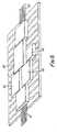
- Referring to Figure 1, a slice of
silicon 2 forms a substrate and has formed thereon an array of precisely positioned and dimensionedsolder pads 4, formed by photolithographic techniques. Thesolder pads 4 are covered with precisely metered amounts of solder 6 by an evaporation technique involving using an accurate dimensioned mask formed by photolithographic techniques. The silicon surface surrounding the pads is non-wettable or repellent to solder. In addition, an array of V-shapedgrooves 8 are formed which extend to one edge of the substrate dimensioned for receiving therein the ends of an array ofoptical fibres 10. Anoptical device 12 formed as a block of material includes optical components comprising ports (waveguides) 14. The lower surface of the block includes an array ofsolder pads 16 formed in the some manner assolder pads 4 and positioned so as to be in one to one correspondence or registration withpads 4. - In order to assemble the optical coupling of Figure 1, the two arrays of
solder pads device 12 above the plane of the substrate to an accuracy of less than 0.5µm, which is sufficient to establish an accurate optical coupling betweenfibres 10 and the optical components. On cooling of the solder, thedevice 12 is rigidly secured to the substrate. - The
fibres 10 may be secured into the V-grooves 8 by solder or other suitable adhesive before or after thesubstrate 2 is attached to the optical device. Verticle alignment of the fibre cores to the optical waveguides is achieved as a consequence of the original photolithography of the V-grooves which establishes the height of the fibre cores to the same as that of theoptical waveguides 12. - Referring now to Figure 2 a substrate of
suitable material 20 has etched into its surface a series of V-grooves 22 and in precise alignment to these an array of solder wettable pads 24. Theends 26 of the V-grooves are also accurately fixed in the same photolithographic step and can be used as an end stop for thefibres 28 in order to set the final spacing of fibres to the optical device. Theoptical device 30 has a corresponding array ofsolder wettable pads 32. Solder can be evaporated or sputtered to either the V-groove substrate 20 or the optical device or both. The fibres may be fixed in the V-groove up to the end stop prior to attachment to the optical device or this can be done after the two are joined. On inverting thesubstrate 20 as shown and reflowing the solder a final fibred assembly is produced. - Referring to Figure 3 two sets of V-
grooves 34, which may be continuous are etched into asuitable substrate 36.Solder wettable pads 38 are again accurately located on thesubstrate 36 andoptical device 40 to provide the final alignment. Also included on the V- groove slab areconductive tracks 42 which have solderwettable areas 44 corresponding to the optical device electrode location. After reflowing the interconnecting solder and insertion of the fibres into the V-grooves the device electrodes can be accessed by wire bonding to the protrudingconductive tracks 42. In addition electrical components may be performed in thesubstrate 36 by known integration techniques in electrical connection withtracks 42. - Figure 4 shows a similar assembly to Figure 3 including solder connected
tracks 42 but in this instance the tracks terminate in plated through holes 46. The holes provide a positive location for the assembly onto a suitable package base 48 with protrudinglegs 49. Reflowing of solder applied to the holes gives electrical and mechanical connection without any further assembly required. The whole assembly may then be protected by encapsulation. - Figure 5 which is a modification of the assembly of Figure 4, shows a method of attaching the
conductive tracks 52 to thepackage legs 54 without the necessity for plated through holes by providingflat end surfaces 56 forlegs 54 registering withtracks 52. Solder or conductive adhesive is applied to the area of contact ofend surfaces 56 andtracks 52 and the inverted assembly is bonded as shown. Plastic encapsulation may be used to protect the whole assembly. - The assembly shown in Figure 6 incorporates a number of
optical devices 60 as well asfibre arrays 62. Theoptical devices 60 each is formed as a block and contains optical components aligned with one another and secured in position by the use of solder aligned pads. Such a system can be assembled in one operation and encapsulated in suitable material to protect it. - The foregoing description shown the invention to be an inexpensive and labour independent method of aligning optical devices and fibres to sub micron accuracy as well as providing for electrical connections to active devices without the use of wire bonding techniques. Standard photolithographic and solder reflow techniques are used and the final assembly can be encapsulated and packaged in conventional configurations.
Claims (10)
Applications Claiming Priority (2)
| Application Number | Priority Date | Filing Date | Title |
|---|---|---|---|
| GB8719557AGB2208943B (en) | 1987-08-19 | 1987-08-19 | Alignment of fibre arrays |
| GB8719557 | 1987-08-19 |
Publications (3)
| Publication Number | Publication Date |
|---|---|
| EP0304118A2true EP0304118A2 (en) | 1989-02-22 |
| EP0304118A3 EP0304118A3 (en) | 1989-11-15 |
| EP0304118B1 EP0304118B1 (en) | 1993-04-14 |
Family
ID=10622478
Family Applications (1)
| Application Number | Title | Priority Date | Filing Date |
|---|---|---|---|
| EP88201696AExpired - LifetimeEP0304118B1 (en) | 1987-08-19 | 1988-08-08 | Alignment of fibre arrays |
Country Status (5)
| Country | Link |
|---|---|
| US (1) | US4892377A (en) |
| EP (1) | EP0304118B1 (en) |
| JP (1) | JP2664214B2 (en) |
| DE (1) | DE3880234T2 (en) |
| GB (1) | GB2208943B (en) |
Cited By (13)
| Publication number | Priority date | Publication date | Assignee | Title |
|---|---|---|---|---|
| EP0370663A3 (en)* | 1988-11-22 | 1991-05-08 | Gec-Marconi Limited | Optical coupling of optical fibres and optical devices |
| EP0507099A1 (en)* | 1991-04-02 | 1992-10-07 | International Business Machines Corporation | Miniature electronic device aligner using capacitance techniques |
| EP0511931A3 (en)* | 1991-04-29 | 1993-03-31 | International Business Machines Corporation | An apparatus and a method for an optical fiber interface |
| US5241614A (en)* | 1991-04-29 | 1993-08-31 | International Business Machines Corporation | Apparatus and a method for an optical fiber interface |
| EP0645651A4 (en)* | 1993-03-31 | 1995-07-19 | Sumitomo Electric Industries | GROUPING OF OPTICAL FIBERS. |
| EP0699931A1 (en)* | 1994-08-31 | 1996-03-06 | Hewlett-Packard Company | Passive alignment and packaging of optoelectronic components to optical waveguides using flip-chip bonding technology |
| WO1997002501A1 (en)* | 1995-06-30 | 1997-01-23 | The Whitaker Corporation | Passive alignment frame using monocrystalline material |
| US5981975A (en)* | 1998-02-27 | 1999-11-09 | The Whitaker Corporation | On-chip alignment fiducials for surface emitting devices |
| US6085007A (en)* | 1998-02-27 | 2000-07-04 | Jiang; Ching-Long | Passive alignment member for vertical surface emitting/detecting device |
| EP1094355A1 (en)* | 1999-10-19 | 2001-04-25 | Corning Incorporated | Electrical interconnection of planar lightwave circuits |
| WO2003017366A1 (en)* | 2001-08-21 | 2003-02-27 | Advanpack Solutions Pte Ltd | Method for forming a flip chip on leadframe semiconductor package |
| EP0718653B1 (en)* | 1994-12-22 | 2005-10-19 | Nec Corporation | Selfaligned optical element and optical wave-guide by means of solder bumps on rectangular pads |
| EP2799000A4 (en)* | 2012-10-12 | 2015-10-21 | Olympus Medical Systems Corp | ENDOSCOPE |
Families Citing this family (29)
| Publication number | Priority date | Publication date | Assignee | Title |
|---|---|---|---|---|
| JPH024204A (en)* | 1988-06-21 | 1990-01-09 | Hitachi Ltd | Mounting method for opto-electronic circuits |
| JPH03141308A (en)* | 1989-07-17 | 1991-06-17 | Nippon Telegr & Teleph Corp <Ntt> | Photodetecting module and production thereof |
| US5046809A (en)* | 1989-09-29 | 1991-09-10 | Siemens Aktiengesellschaft | Coupling arrangement for optically coupling a fiber to a planar optical waveguide integrated on a substrate |
| CA2077161A1 (en)* | 1991-09-13 | 1993-03-14 | Thomas W. Fitzgerald | Method of establishing soldered connections |
| JPH0688917A (en)* | 1991-11-07 | 1994-03-29 | Nec Corp | Method for connecting optical waveguide element and optical fiber terminal |
| JP2976642B2 (en)* | 1991-11-07 | 1999-11-10 | 日本電気株式会社 | Optical coupling circuit |
| WO1993015424A1 (en)* | 1992-01-28 | 1993-08-05 | British Telecommunications Public Limited Company | Alignment of integrated optical components |
| EP0562211A1 (en)* | 1992-03-25 | 1993-09-29 | International Business Machines Corporation | Self-aligning fiber couplers |
| KR0155508B1 (en)* | 1994-11-30 | 1998-10-15 | 정선종 | Method for self-aligning between optical fiber and optic device |
| JPH09138325A (en)* | 1995-11-13 | 1997-05-27 | Nec Corp | Optical fiber packaging structure and its production |
| US5768457A (en)* | 1995-11-30 | 1998-06-16 | Lucent Technologies Inc. | Multilayered connector pads for supporting butt-joined optical arrays |
| JP3792358B2 (en)* | 1997-07-30 | 2006-07-05 | 京セラ株式会社 | Optical connection component and manufacturing method thereof |
| US6174092B1 (en) | 1999-01-11 | 2001-01-16 | Oesys Photonics, Inc. | Method and apparatus for coupling an optical fiber to an optoelectronic device |
| GB2356463B (en)* | 1999-11-16 | 2003-06-25 | Marconi Electronic Syst Ltd | Method of alignment in an optoelectronic assembly |
| US6443631B1 (en) | 2001-02-20 | 2002-09-03 | Avanti Optics Corporation | Optical module with solder bond |
| US6956999B2 (en) | 2001-02-20 | 2005-10-18 | Cyberoptics Corporation | Optical device |
| US20040212802A1 (en)* | 2001-02-20 | 2004-10-28 | Case Steven K. | Optical device with alignment compensation |
| US6546172B2 (en)* | 2001-02-20 | 2003-04-08 | Avanti Optics Corporation | Optical device |
| US6546173B2 (en)* | 2001-02-20 | 2003-04-08 | Avanti Optics Corporation | Optical module |
| GB2374157B (en)* | 2001-04-06 | 2003-06-25 | Bookham Technology Plc | Mounting an optical fibre using a retaining channel |
| GB2381593A (en)* | 2001-10-30 | 2003-05-07 | Bookham Technology Plc | Optical device with optically connected planar lightwave circuits |
| KR20040009814A (en)* | 2002-07-26 | 2004-01-31 | 우리로광통신주식회사 | Fabrication method of 1 channel fiber-array |
| GB2408111A (en)* | 2002-08-20 | 2005-05-18 | Cyberoptics Corp | Optical alignment mount with height adjustment |
| US7499614B2 (en) | 2003-10-24 | 2009-03-03 | International Business Machines Corporation | Passive alignment of VCSELs to waveguides in opto-electronic cards and printed circuit boards |
| KR101667464B1 (en)* | 2011-11-16 | 2016-10-18 | 미쓰비시덴키 가부시키가이샤 | Semiconductor laser-excitation solid-state laser |
| GB2555398B (en)* | 2016-10-24 | 2020-04-08 | Toshiba Kk | An optoelectronic system and method for its fabrication |
| JP6933794B2 (en)* | 2016-12-01 | 2021-09-08 | 富士通株式会社 | Optical module and manufacturing method of optical module |
| US11719898B2 (en)* | 2021-03-03 | 2023-08-08 | Marvell Asia Pte Ltd. | Methods for co-packaging optical modules on switch package substrate |
| CN113696524A (en)* | 2021-08-11 | 2021-11-26 | 苏州易锐光电科技有限公司 | Micro-nano processing method of optical device |
Family Cites Families (14)
| Publication number | Priority date | Publication date | Assignee | Title |
|---|---|---|---|---|
| US3871014A (en)* | 1969-08-14 | 1975-03-11 | Ibm | Flip chip module with non-uniform solder wettable areas on the substrate |
| US3871015A (en)* | 1969-08-14 | 1975-03-11 | Ibm | Flip chip module with non-uniform connector joints |
| US3963920A (en)* | 1975-03-10 | 1976-06-15 | General Dynamics Corporation | Integrated optical-to-electrical signal transducing system and apparatus |
| GB2137807B (en)* | 1983-04-05 | 1987-08-12 | Plessey Co Plc | A semiconductor component and method of manufacture |
| JPS59185306A (en)* | 1983-04-07 | 1984-10-20 | Agency Of Ind Science & Technol | Method for mounting optical integrated circuit |
| JPS60188909A (en)* | 1984-03-08 | 1985-09-26 | Canon Inc | Manufacture of grating coupler |
| DE3568517D1 (en)* | 1984-04-06 | 1989-04-06 | Plessey Overseas | Improvements relating to the fabrication of optical devices |
| JPS62500471A (en)* | 1984-09-28 | 1987-02-26 | アメリカン テレフオン アンド テレグラフ カムパニ− | Optical waveguide lateral alignment device |
| JPS61173206A (en)* | 1985-01-29 | 1986-08-04 | Fujitsu Ltd | How to fix the optical coupling part |
| JP2513599B2 (en)* | 1985-02-27 | 1996-07-03 | 富士通株式会社 | Method for manufacturing optical waveguide substrate |
| DE3531734A1 (en)* | 1985-09-05 | 1987-03-12 | Siemens Ag | DEVICE FOR POSITIONING A SEMICONDUCTOR LASER WITH SELF-ADJUSTING EFFECT FOR A FIBER TO BE COUPLED |
| GB8522429D0 (en)* | 1985-09-10 | 1985-10-16 | Plessey Co Plc | Alignment for hybrid device |
| DE3534017A1 (en)* | 1985-09-24 | 1987-03-26 | Siemens Ag | METHOD FOR COUPLING A LASER DIODE TO A MONOMODE LIGHT WAVE GUIDE, AND AN ARRANGEMENT OF A LASER DIODE AND A LIGHT WAVE GUIDE COUPLED TO IT |
| DE3538556C2 (en)* | 1985-10-30 | 1995-12-14 | Ant Nachrichtentech | Device for the mutual alignment of two optical components to be coupled together |
- 1987
- 1987-08-19GBGB8719557Apatent/GB2208943B/ennot_activeExpired - Lifetime
- 1988
- 1988-08-08DEDE8888201696Tpatent/DE3880234T2/ennot_activeExpired - Fee Related
- 1988-08-08EPEP88201696Apatent/EP0304118B1/ennot_activeExpired - Lifetime
- 1988-08-18JPJP63205663Apatent/JP2664214B2/ennot_activeExpired - Fee Related
- 1988-08-19USUS07/233,757patent/US4892377A/ennot_activeExpired - Lifetime
Cited By (21)
| Publication number | Priority date | Publication date | Assignee | Title |
|---|---|---|---|---|
| EP0370663A3 (en)* | 1988-11-22 | 1991-05-08 | Gec-Marconi Limited | Optical coupling of optical fibres and optical devices |
| EP0507099A1 (en)* | 1991-04-02 | 1992-10-07 | International Business Machines Corporation | Miniature electronic device aligner using capacitance techniques |
| EP0511931A3 (en)* | 1991-04-29 | 1993-03-31 | International Business Machines Corporation | An apparatus and a method for an optical fiber interface |
| US5241614A (en)* | 1991-04-29 | 1993-08-31 | International Business Machines Corporation | Apparatus and a method for an optical fiber interface |
| US5764833A (en)* | 1993-03-31 | 1998-06-09 | Sumitomo Electric Industries, Ltd. | Optical fiber array |
| EP0645651A4 (en)* | 1993-03-31 | 1995-07-19 | Sumitomo Electric Industries | GROUPING OF OPTICAL FIBERS. |
| US5548677A (en)* | 1993-03-31 | 1996-08-20 | Sumitomo Electric Industries, Ltd. | Housing structure for coupling and releasing optical modules |
| EP0860721A1 (en)* | 1993-03-31 | 1998-08-26 | Sumitomo Electric Industries, Ltd. | Optical fiber array |
| US5719978A (en)* | 1993-03-31 | 1998-02-17 | Sumitomo Electric Industries, Ltd. | Parallel transmission module for transmitting a plurality of optical signals in parallel and method for manufacturing the same |
| EP0699931A1 (en)* | 1994-08-31 | 1996-03-06 | Hewlett-Packard Company | Passive alignment and packaging of optoelectronic components to optical waveguides using flip-chip bonding technology |
| EP1120673A1 (en)* | 1994-08-31 | 2001-08-01 | Agilent Technologies Inc. | Passive alignment of optoelectronic components to optical waveguides using flip-chip bonding technology |
| EP0718653B1 (en)* | 1994-12-22 | 2005-10-19 | Nec Corporation | Selfaligned optical element and optical wave-guide by means of solder bumps on rectangular pads |
| WO1997002501A1 (en)* | 1995-06-30 | 1997-01-23 | The Whitaker Corporation | Passive alignment frame using monocrystalline material |
| US5905831A (en)* | 1995-06-30 | 1999-05-18 | The Whitaker Corporation | Passive alignment frame using monocrystalline material |
| US5981975A (en)* | 1998-02-27 | 1999-11-09 | The Whitaker Corporation | On-chip alignment fiducials for surface emitting devices |
| US6085007A (en)* | 1998-02-27 | 2000-07-04 | Jiang; Ching-Long | Passive alignment member for vertical surface emitting/detecting device |
| EP1094355A1 (en)* | 1999-10-19 | 2001-04-25 | Corning Incorporated | Electrical interconnection of planar lightwave circuits |
| US6327408B1 (en) | 1999-10-19 | 2001-12-04 | Corning Incorporated | Electrical interconnection of planar lightwave circuits |
| WO2003017366A1 (en)* | 2001-08-21 | 2003-02-27 | Advanpack Solutions Pte Ltd | Method for forming a flip chip on leadframe semiconductor package |
| EP2799000A4 (en)* | 2012-10-12 | 2015-10-21 | Olympus Medical Systems Corp | ENDOSCOPE |
| US9380929B2 (en) | 2012-10-12 | 2016-07-05 | Olympus Corporation | Endoscope with an optical member, a frame portion and a bonding member soldering the optical member to the frame portion |
Also Published As
| Publication number | Publication date |
|---|---|
| GB8719557D0 (en) | 1987-09-23 |
| GB2208943B (en) | 1991-07-31 |
| DE3880234D1 (en) | 1993-05-19 |
| JPH01140104A (en) | 1989-06-01 |
| EP0304118A3 (en) | 1989-11-15 |
| JP2664214B2 (en) | 1997-10-15 |
| US4892377A (en) | 1990-01-09 |
| GB2208943A (en) | 1989-04-19 |
| EP0304118B1 (en) | 1993-04-14 |
| DE3880234T2 (en) | 1993-09-16 |
Similar Documents
| Publication | Publication Date | Title |
|---|---|---|
| US4892377A (en) | Alignment of fibre arrays | |
| US4867371A (en) | Fabrication of optical devices | |
| EP0331331B1 (en) | Subassembly for optoelectronic devices | |
| KR100441810B1 (en) | Electronic device to align light transmission structures | |
| US5205032A (en) | Electronic parts mounting apparatus | |
| KR100481023B1 (en) | Optical device with chip level precision alignment | |
| EP0529947B1 (en) | Optical assembly for aligning an active optical device and an optical fiber and method of forming such assembly | |
| CA2128534C (en) | Alignment of integrated optical components | |
| JP3403306B2 (en) | Optical module | |
| KR100442609B1 (en) | Structure of flip chip bonding and method for bonding | |
| KR19980069992A (en) | Method for mounting a compound unit of an optical semiconductor device and a support substrate and an optical semiconductor device on a support substrate | |
| US20030228084A1 (en) | Printed board unit for optical transmission and mounting method | |
| EP0218624B1 (en) | Improvements relating to optical connecting arrangements | |
| US5522000A (en) | Providing optical coupling with single crystal substrate mounted electro-optic transducers | |
| JP2001343560A (en) | Optical module | |
| KR100211039B1 (en) | Optical switch-optical fiber optical coupler | |
| EP1184696A1 (en) | Self-aligning optical component assembly on a common substrate | |
| JP3709075B2 (en) | Optical element mounting method | |
| JPH03184384A (en) | Optical module submount and manufacture thereof | |
| US6628000B1 (en) | Techniques for maintaining parallelism between optical and chip sub-assemblies | |
| US20010050430A1 (en) | Electronic assembly having high interconnection density | |
| KR100271826B1 (en) | Optical alignment between laser diode and optical fiber using inp v-groove | |
| KR0142524B1 (en) | Height Control and Thermal Characteristics Improvement Method of Flip Chip Bonded Optical Device | |
| KR0173912B1 (en) | Optical connection device of optical waveguide and input / output terminal single mode optical fiber and its manufacturing method |
Legal Events
| Date | Code | Title | Description |
|---|---|---|---|
| PUAI | Public reference made under article 153(3) epc to a published international application that has entered the european phase | Free format text:ORIGINAL CODE: 0009012 | |
| AK | Designated contracting states | Kind code of ref document:A2 Designated state(s):BE CH DE ES FR IT LI NL SE | |
| PUAL | Search report despatched | Free format text:ORIGINAL CODE: 0009013 | |
| AK | Designated contracting states | Kind code of ref document:A3 Designated state(s):BE CH DE ES FR IT LI NL SE | |
| 17P | Request for examination filed | Effective date:19900406 | |
| 17Q | First examination report despatched | Effective date:19920131 | |
| RAP1 | Party data changed (applicant data changed or rights of an application transferred) | Owner name:GEC-MARCONI LIMITED | |
| GRAA | (expected) grant | Free format text:ORIGINAL CODE: 0009210 | |
| AK | Designated contracting states | Kind code of ref document:B1 Designated state(s):BE CH DE ES FR IT LI NL SE | |
| PG25 | Lapsed in a contracting state [announced via postgrant information from national office to epo] | Ref country code:SE Effective date:19930414 Ref country code:LI Effective date:19930414 Ref country code:ES Free format text:THE PATENT HAS BEEN ANNULLED BY A DECISION OF A NATIONAL AUTHORITY Effective date:19930414 Ref country code:CH Effective date:19930414 Ref country code:BE Effective date:19930414 | |
| ITF | It: translation for a ep patent filed | ||
| ET | Fr: translation filed | ||
| REF | Corresponds to: | Ref document number:3880234 Country of ref document:DE Date of ref document:19930519 | |
| REG | Reference to a national code | Ref country code:CH Ref legal event code:PL | |
| PLBE | No opposition filed within time limit | Free format text:ORIGINAL CODE: 0009261 | |
| STAA | Information on the status of an ep patent application or granted ep patent | Free format text:STATUS: NO OPPOSITION FILED WITHIN TIME LIMIT | |
| PG25 | Lapsed in a contracting state [announced via postgrant information from national office to epo] | Ref country code:NL Effective date:19940301 | |
| 26N | No opposition filed | ||
| NLV4 | Nl: lapsed or anulled due to non-payment of the annual fee | ||
| PG25 | Lapsed in a contracting state [announced via postgrant information from national office to epo] | Ref country code:FR Effective date:19940429 | |
| PG25 | Lapsed in a contracting state [announced via postgrant information from national office to epo] | Ref country code:DE Effective date:19940503 | |
| REG | Reference to a national code | Ref country code:FR Ref legal event code:ST | |
| PG25 | Lapsed in a contracting state [announced via postgrant information from national office to epo] | Ref country code:IT Free format text:LAPSE BECAUSE OF NON-PAYMENT OF DUE FEES Effective date:20050808 |