EP0300754B1 - Display device - Google Patents
Display deviceDownload PDFInfo
- Publication number
- EP0300754B1 EP0300754B1EP88306636AEP88306636AEP0300754B1EP 0300754 B1EP0300754 B1EP 0300754B1EP 88306636 AEP88306636 AEP 88306636AEP 88306636 AEP88306636 AEP 88306636AEP 0300754 B1EP0300754 B1EP 0300754B1
- Authority
- EP
- European Patent Office
- Prior art keywords
- pulse
- liquid crystal
- electrodes
- crystal layer
- switching
- Prior art date
- Legal status (The legal status is an assumption and is not a legal conclusion. Google has not performed a legal analysis and makes no representation as to the accuracy of the status listed.)
- Expired - Lifetime
Links
- 239000004973liquid crystal related substanceSubstances0.000claimsdescription37
- 238000000034methodMethods0.000claimsdescription23
- 210000002858crystal cellAnatomy0.000claimsdescription8
- 239000005262ferroelectric liquid crystals (FLCs)Substances0.000claimsdescription8
- 210000004027cellAnatomy0.000claimsdescription2
- 239000000463materialSubstances0.000description14
- 230000000694effectsEffects0.000description11
- 239000011159matrix materialSubstances0.000description6
- 230000005684electric fieldEffects0.000description5
- 235000010290biphenylNutrition0.000description3
- 239000004305biphenylSubstances0.000description3
- -1biphenyl esterChemical class0.000description3
- ZUOUZKKEUPVFJK-UHFFFAOYSA-NphenylbenzeneNatural productsC1=CC=CC=C1C1=CC=CC=C1ZUOUZKKEUPVFJK-UHFFFAOYSA-N0.000description3
- 239000003990capacitorSubstances0.000description2
- 238000010586diagramMethods0.000description2
- 230000003287optical effectEffects0.000description2
- 101100041822Schizosaccharomyces pombe (strain 972 / ATCC 24843) sce3 geneProteins0.000description1
- 230000015556catabolic processEffects0.000description1
- 230000001186cumulative effectEffects0.000description1
- 230000007423decreaseEffects0.000description1
- 238000006731degradation reactionMethods0.000description1
- 239000011521glassSubstances0.000description1
- 238000009413insulationMethods0.000description1
- 239000007788liquidSubstances0.000description1
- 230000007774longtermEffects0.000description1
- 230000001151other effectEffects0.000description1
- 238000005070samplingMethods0.000description1
- 238000004088simulationMethods0.000description1
- 230000001360synchronised effectEffects0.000description1
Images


Classifications
- G—PHYSICS
- G09—EDUCATION; CRYPTOGRAPHY; DISPLAY; ADVERTISING; SEALS
- G09G—ARRANGEMENTS OR CIRCUITS FOR CONTROL OF INDICATING DEVICES USING STATIC MEANS TO PRESENT VARIABLE INFORMATION
- G09G3/00—Control arrangements or circuits, of interest only in connection with visual indicators other than cathode-ray tubes
- G09G3/20—Control arrangements or circuits, of interest only in connection with visual indicators other than cathode-ray tubes for presentation of an assembly of a number of characters, e.g. a page, by composing the assembly by combination of individual elements arranged in a matrix no fixed position being assigned to or needed to be assigned to the individual characters or partial characters
- G09G3/34—Control arrangements or circuits, of interest only in connection with visual indicators other than cathode-ray tubes for presentation of an assembly of a number of characters, e.g. a page, by composing the assembly by combination of individual elements arranged in a matrix no fixed position being assigned to or needed to be assigned to the individual characters or partial characters by control of light from an independent source
- G09G3/36—Control arrangements or circuits, of interest only in connection with visual indicators other than cathode-ray tubes for presentation of an assembly of a number of characters, e.g. a page, by composing the assembly by combination of individual elements arranged in a matrix no fixed position being assigned to or needed to be assigned to the individual characters or partial characters by control of light from an independent source using liquid crystals
- G09G3/3611—Control of matrices with row and column drivers
- G09G3/3685—Details of drivers for data electrodes
- G09G3/3692—Details of drivers for data electrodes suitable for passive matrices only
- G—PHYSICS
- G09—EDUCATION; CRYPTOGRAPHY; DISPLAY; ADVERTISING; SEALS
- G09G—ARRANGEMENTS OR CIRCUITS FOR CONTROL OF INDICATING DEVICES USING STATIC MEANS TO PRESENT VARIABLE INFORMATION
- G09G3/00—Control arrangements or circuits, of interest only in connection with visual indicators other than cathode-ray tubes
- G09G3/20—Control arrangements or circuits, of interest only in connection with visual indicators other than cathode-ray tubes for presentation of an assembly of a number of characters, e.g. a page, by composing the assembly by combination of individual elements arranged in a matrix no fixed position being assigned to or needed to be assigned to the individual characters or partial characters
- G09G3/34—Control arrangements or circuits, of interest only in connection with visual indicators other than cathode-ray tubes for presentation of an assembly of a number of characters, e.g. a page, by composing the assembly by combination of individual elements arranged in a matrix no fixed position being assigned to or needed to be assigned to the individual characters or partial characters by control of light from an independent source
- G09G3/36—Control arrangements or circuits, of interest only in connection with visual indicators other than cathode-ray tubes for presentation of an assembly of a number of characters, e.g. a page, by composing the assembly by combination of individual elements arranged in a matrix no fixed position being assigned to or needed to be assigned to the individual characters or partial characters by control of light from an independent source using liquid crystals
- G09G3/3611—Control of matrices with row and column drivers
- G09G3/3622—Control of matrices with row and column drivers using a passive matrix
- G09G3/3629—Control of matrices with row and column drivers using a passive matrix using liquid crystals having memory effects, e.g. ferroelectric liquid crystals
- G—PHYSICS
- G09—EDUCATION; CRYPTOGRAPHY; DISPLAY; ADVERTISING; SEALS
- G09G—ARRANGEMENTS OR CIRCUITS FOR CONTROL OF INDICATING DEVICES USING STATIC MEANS TO PRESENT VARIABLE INFORMATION
- G09G3/00—Control arrangements or circuits, of interest only in connection with visual indicators other than cathode-ray tubes
- G09G3/20—Control arrangements or circuits, of interest only in connection with visual indicators other than cathode-ray tubes for presentation of an assembly of a number of characters, e.g. a page, by composing the assembly by combination of individual elements arranged in a matrix no fixed position being assigned to or needed to be assigned to the individual characters or partial characters
- G09G3/34—Control arrangements or circuits, of interest only in connection with visual indicators other than cathode-ray tubes for presentation of an assembly of a number of characters, e.g. a page, by composing the assembly by combination of individual elements arranged in a matrix no fixed position being assigned to or needed to be assigned to the individual characters or partial characters by control of light from an independent source
- G09G3/36—Control arrangements or circuits, of interest only in connection with visual indicators other than cathode-ray tubes for presentation of an assembly of a number of characters, e.g. a page, by composing the assembly by combination of individual elements arranged in a matrix no fixed position being assigned to or needed to be assigned to the individual characters or partial characters by control of light from an independent source using liquid crystals
- G09G3/3611—Control of matrices with row and column drivers
- G09G3/3674—Details of drivers for scan electrodes
- G09G3/3681—Details of drivers for scan electrodes suitable for passive matrices only
- G—PHYSICS
- G09—EDUCATION; CRYPTOGRAPHY; DISPLAY; ADVERTISING; SEALS
- G09G—ARRANGEMENTS OR CIRCUITS FOR CONTROL OF INDICATING DEVICES USING STATIC MEANS TO PRESENT VARIABLE INFORMATION
- G09G2310/00—Command of the display device
- G09G2310/06—Details of flat display driving waveforms
- G—PHYSICS
- G09—EDUCATION; CRYPTOGRAPHY; DISPLAY; ADVERTISING; SEALS
- G09G—ARRANGEMENTS OR CIRCUITS FOR CONTROL OF INDICATING DEVICES USING STATIC MEANS TO PRESENT VARIABLE INFORMATION
- G09G2330/00—Aspects of power supply; Aspects of display protection and defect management
- G09G2330/02—Details of power systems and of start or stop of display operation
Definitions
- the present inventionrelates to a method of addressing a matrix-array type liquid crystal cell with a ferroelectric liquid crystal layer having a plurality of pixels defined by areas of overlap between members of a first set of electrodes on one side of the liquid crystal layer and members of a second set of electrodes on the other side of the liquid crystal layer, each of said pixels having a first and a second optically distinguishable state, and having a response time for switching between said first and said second states which depends on the potential difference across the liquid crystal layer, the method including the step of applying charge-balanced strobe and data waveforms to first and second electrodes respectively of a selected pixel to produce a resultant charge-balanced waveform there-between to switch the selected pixel between said first and second states, the strobe and data signals being such that the resultant waveform comprises a switching pulse having a pulse width and a pulse height magnitude which in combination switch the selected pixel and another pulse, at least contributing to charge-balancing, having a pulse height magnitude greater than the pulse height magnitude of the
- a liquid crystal materialconsists of long thin polar molecules and so can preserve a high degree of long range orientational ordering of the molecules in a liquid condition.
- Such materialsare anisotropic with properties, such as dielectric constant, characterised by two constants, one in the direction of the long molecular axis and one perpendicular to it.
- dielectric constantcharacterised by two constants, one in the direction of the long molecular axis and one perpendicular to it.
- the anisotropic nature of the dielectric constantenables the molecules to be aligned in an electric field, the molecules tending to be orientated in the direction giving the minimum electrostatic free energy.
- liquid crystal materialsalso exhibit ferroelectric properties i.e. they have a permanent dipole moment which is perpendicular to the long molecular axis.
- ferroelectric propertiesi.e. they have a permanent dipole moment which is perpendicular to the long molecular axis.
- the moleculesWhen the liquid crystal material is placed between two glass plates whose surfaces have been treated to align the molecules, then the molecules will have two possible states depending on the direction of the permanent dipole moment. These states are bistable. By applying an electric field of the correct amplitude and polarity, it is possible to switch the molecules between the two states.
- the pixels of the matrixare defined by areas of overlap between members of a first set of electrodes on one side of the liquid crystal layer and members of a second set of electrodes on the other side of the liquid crystal layer.
- An electric fieldis applied across the molecules of a pixel by the generation of voltages at the member of the first set of electrodes and the member of the second set of electrodes that define the pixel.
- the individual electrodescan be either in electrical contact with or insulated from the liquid crystal layer.
- there is a risk of electrolytic degradation of the liquid crystalif there is a nett flow of direct current through the layer.
- GB-A-2 173 335discloses a method of addressing a matrix addressed ferroelectric liquid crystal cell in which a switching pulse of height (V s +V d ) and width t s is charge balanced by three pulses of the opposite polarity - one of height -(V s -V d ) and width t s and two of height mV d and width t s /m where m is a factor greater than unity.
- the documentsuggests that such a method can be used with a display device in which the liquid crystal material can tolerate a reverse polarity of the same duration but only 75% of the amplitude of a pulse that is just sufficient to effect switching.
- the minimum line address timei.e. the minimum time necessary to generate a voltage waveform including a switching pulse and charge-balancing pulses
- the minimum line address timeis 2t s (1+1/m) .
- the inventorshave noted that the width of a pulse has more effect on the tendency of the pixel to switch than the pulse height.
- the present inventionmakes use of this discovery.
- a method as defined in the first paragraphwhich is characterised in that the strobe and data waveforms are such that the switching pulse is charge-balanced by said another pulse alone and non-zero portions of the strobe and data waveforms overlap so that the pixel is charge-balanced addressed with a waveform having a duration less than twice that of the switching pulse.
- the first pulsei.e. the switching pulse
- the first pulseis charge-balanced.
- This charge-balancingis, by a second pulse having a pulse height magnitude greater than that of the first pulse.
- the pulse width of the second pulseis accordingly less than the pulse width of the first pulse and so the minimum address time of the method can be less than twice the pulse width of the first pulse. This is a reduction in minimum line address time compared with prior art charge-balanced switching waveforms.
- whether or not a pulse is a switching pulseis, in the present invention, being determined by its pulse width.
- the term 'slot'can have one or two meanings i.e. 1) the minimum time that a liquid crystal material takes to switch from a first state to a second state for a given pulse height; 2) the time for which a waveform is at a (given) constant voltage, i.e. the pulse width of a pulse of a given pulse height.
- meaning (2)is more common in the art, this will be the meaning intended in the present specification unless otherwise indicated. Also unless otherwise indicated the term used in the present specification for meaning (1) will be 'response time, t s '.
- Figure 1shows, schematically, part of a matrix-array type liquid crystal cell 2 with a layer formed of a ferroelectric liquid crystal material such as a biphenyl ester sold under the trade name BDH SCE3 and having a thickness in the range of from 1.4 ⁇ m to 2.0 ⁇ m.
- the pixels 4 of the matrixare defined by areas of overlap between members of a first set of row electrodes 6 on one side of the liquid crystal layer and members of a second set of column electrodes 8 on the other side of the liquid crystal layer. For each pixel, the electric field thereacross determines the state and hence alignment of the liquid crystal molecules.
- Parallel polarizers(not shown) are provided at either side of the cell 2.
- each pixelhas a first and a second optically distinguishable state provided by the two bistable states of the liquid crystal molecules in that pixel.
- Voltage waveformsare applied to the row electrodes 6 and column electrodes 8 respectively by row drivers 10 and column drivers 12.
- the matrix of pixels 4is addressed on a line-by-line basis by applying voltage waveforms, termed strobe waveforms, serially to the row electrodes 6 while voltage waveforms, termed data waveforms, are applied in parallel to the column electrodes 8.
- the resultant waveform across a pixel defined by a row electrode and a column electrodeis given by the potential difference between the waveform applied to that row electrode and the waveform applied to that column electrode.
- Figure 2shows an arrangement embodying the present invention.
- the arrangementutilizes a 1.5 slot in the sense of a slot being the minimum time that the material takes to switch, i.e. 1.5t s .
- the driver output voltageshave to change 6 times and 5 output states are required.
- the top left hand strobe waveformappears on the selected row. Unselected i,e, unstrobed rows have a constant 0 volts applied.
- the second row on the diagramshows the column or data waveforms. These have been arranged to consist of bipolar pulses to minimise their switching effect on unselected rows.
- the resultant pixel waveforms for a selected roware shown above the respective column waveforms.
- a pixel being switched offreceives a long low voltage negative pulse followed by a short high voltage positive one of equivalent area maintaining zero D.C. content.
- a pixel being switched onreceives a short high voltage negative equalising pulse followed by a long low voltage positive switching pulse.
- Related schemesare shown in Figures 3, 4 and 5 giving alternative equalisation pulse shapes.
- Each of the arrangements shown in Figures 2 to 5uses the fact that a switching pulse having a sufficient pulse width and pulse height magnitude to switch a pixel can be charge-balanced by a non-switching pulse of less pulse width, i.e. insufficient to switch the pixel, but of greater pulse height magnitude.
- one of two waveforms - a bipolar strobe waveform or a constant zero-voltage waveform -can be applied to each row electrode, the row electrode to which the strobe waveform is applied being the selected row.
- One of two data waveforms - a column 'off' waveform or a column 'on' waveform -can be applied to each column electrode.
- both the data waveformsare bipolar waveforms
- the resulting pixel waveforms on unstrobed rowshave no net effect on the pixels of those rows and so the pixels do not switch states.
- the combination of the bipolar strobe waveform and either one of the data waveformsproduces a resulting pixel waveform which is a switching pixel waveform.
- Such a waveformas shown in Figures 2 to 5, consists of a first pulse, i.e.
- the arrangement of Figure 5differs from the arrangement of Figures 2 to 4 in that in the switching pulse itself can be distinguished two pulses, one of which has a smaller pulse height magnitude than the other, the width of the total pulse being sufficient to switch a selected pixel at the smaller pulse height magnitude.
- the minimum line address time of each arrangementis less than twice the response time t s of the liquid crystal material at the pulse height of the switching pulse.
- the line address timeis 1.5t s
- the line address timeis 1.3t s .
- the line address time of the arrangement of Figure 4is less than that of the arrangements of Figures 2, 3 and 5 but at the expense of requiring more output states.
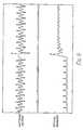
- FIG. 6shows the electro-optic characteristic of a ferroelectric liquid crystal material, such as the aforementioned biphenyl ester, which is suitable for use in a matrix-array type liquid crystal cell addressed by the method of the present invention.
- An electro-optic characteristicis a graph showing response time of a liquid crystal material against potential difference across the material. As there is a minimum in the characteristic, pulses of a width less than t m will not switch the pixel irrespective of the height of the pulse.
- a switching pulse of height V1 and width t1can be charge balanced by a pulse of height V2 greater than V1 and width t2, which width t2 less than t m is a width insufficient to switch a pixel irrespective of the pulse height.
- the method of the present inventioncan be used to address a matrix-array type liquid crystal cell with a liquid crystal material, such as a flouro-terphenyl, having an electro-optic characteristic as shown in Figure 7, in which the response time t s decreases asymptotically with potential difference.
- a switching pulse of height V3 and width t3is charge balanced by a pulse of height V4 greater than V3 and width t4, which width t4 is insufficient in relation to the height V4 to switch the selected pixel.
- pulse heightas well as by pulse width. Both pulse width and pulse height would also have to be considered in the case where the electro-optic characteristic does have a minimum but the pulse height and width of the switching pulse are such that charge-balancing can be provided by a pulse of width greater than t m .
- the relatively complex waveforms of Figures 2 to 5need not be generated independently at each row or column driver. In each case the row or column output stage need only switch between one of the two waveforms.
- Figures 8 and 9show an oscilloscope trace of the switching voltage, i.e. resulting pixel waveform, and optical response resulting from a simulation of the proposed scheme.
- Figure 8shows that the liquid crystal is switching between the two optically distinguishable states and remaining stable while the row is not being selected; the switching waveform is too fast for the oscilloscope sampling.
- Figure 9shows in more detail the switching point S. Switching occurs when the wide pulse is applied. The narrower equalisation and crosstalk pulses serve to stabilise the pixel state.
- Display driver chipsare available which have multiple high voltage CMOS outputs and take the form of n stage shift registers with latched outputs. These chips were originally designed for use with ACEL displays but they are now being used in a number of LCD implementations. An apparent limitation of these devices is that the outputs are two state. The output voltage is either at the high voltage or at ground. This limitation is removed by using the proposed arrangement and method.
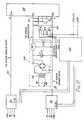
- FIG. 10shows a block diagram representing this arrangement and method.
- the drive circuitcomprises means 20 to generate a first waveform A at a first supply rail 21 and means 22 to generate a second waveform B at a second supply rail 23 which acts as ground potential for the circuit.
- a display driver chip 24has a plurality of outputs, each including a switch for switching the output either to waveform A at the first supply rail 21 or to waveform B at the second supply rail 23. Accordingly a respective output waveform is produced at each of the plurality of outputs.
- each output to either waveform A or to waveform Bis controlled by control and output latch data from a control circuit (not shown).
- the datais fed to the driver chip 24 via means to isolate the data waveforms so that these will be relative to the supply rail 23, such as opto-isolators 26. If the logic for an output is '1' then the output is switched to waveform A at supply rail 21; if the logic is '0' then the output is switched to waveform B at supply rail 23.
- the power supply to the driver chip 24comprises an isolated power supply 28 to provide a constant 12V potential difference with respect to the potential of the ground supply rail 23.
- Waveforms X and Y at supply rails 30 and 32are generated by first and second 4-way high voltage multiplexers 34, 36.
- Each multiplexer 34, 36is capable of generating four voltage states, e.g.
- V e35V can be used.
- the display driver chip 38 of the circuitis an Si 9555 (manufactured under the trade mark 'Siliconix') having 32 channels, i.e. a 32 bit stage shift register, 32 latches and 32 outputs. Each one of the outputs is switched to either the voltage of supply rail 30 (i.e. waveform X) by a logic input of '1' or to the voltage of supply rail 32 (i.e. waveform Y) by a logic input of 'O'.
- FIG. 11shows three outputs from the gate array 40 connected to respective three inputs of the driver chip 38 via three opto-isolators (designated generally by the reference 42).
- the three inputs showncomprise a clock input and a data input which load logic serially into the 32-bit stage shift register, and a latch enable which, when high, shifts the contacts of the 32 bit stage shift register into an output register, in known manner.
- Poweris supplied to the gate array 40 itself by two supply rails at -2V e and -2V e + 5V.
- the driver chip 38is powered by a 12V constant DC supply produced by an isolated power supply 44 connected across a positive power supply rail 45 and the ground supply rail 32.
- Inputs 46, 48 to the power supply 44are connected to a 240V AC mains supply.
- the voltageis transformed down at a transformer 50 and rectified at a full wave rectifier 52.
- the power supply 44further comprises a 10,000 ⁇ F electrolytic capacitor C1, a 7812 voltage regulator 54 and a 100nF capacitor C2.
- the 12V constant DC supply producedis constant with respect to the ground supply rail 32 and accordingly the positive power supply rail 45 has superimposed thereon the voltage of waveform Y.
- a typical display devicehas of the order of several hundred row and column electrodes and accordingly a large number of driver chips are required.
- a single multiplexer 34, multiplexer 36, isolated power supply 44 and gate array 40can be provided for a set of row or column electrodes and corresponding driver chips.
- the chipis effectively being used as a set of analogue switches.
- the latches and the shift registerare powered separately to the high voltage output stage so their operation is not affected, provided the power is maintained with respect to the ground (waveform B).
- Any of the outputscan be switched to either waveform A or waveform B.
- the only limitationis that the instantaneous voltage of waveform A must never be less than that of waveform B by more than two diode forward voltage drops. If the two alternative row or column drive waveforms cross then the contents of the output latches can be inverted and the waveforms interchanged.
- Figure 12shows how this method and arrangement can be used to implement the arrangement of Figure 3.
- the left hand columnshows the waveforms for a drive circuit for the row electrodes and the right hand column shows the waveforms for a drive circuit for the column electrodes.
- Figures 12a and 12bshow the waveforms A and B applied to the supply rails of the row drive circuit.
- the strobed waveform( Figure 12c) is produced by a data sequence of 000111 and the unstrobed waveform (Figure 12d) by a data sequence of 111000.
- Figures 12e and 12fshow the waveforms A and B applied to the supply rails of the column drive circuit.
- the column 'on' waveform( Figure 12g) is produced by a data sequence of 110011 and the column 'off' waveform (Figure 12h) by a data sequence of 001100.
Landscapes
- Engineering & Computer Science (AREA)
- Chemical & Material Sciences (AREA)
- Crystallography & Structural Chemistry (AREA)
- Physics & Mathematics (AREA)
- Computer Hardware Design (AREA)
- General Physics & Mathematics (AREA)
- Theoretical Computer Science (AREA)
- Liquid Crystal Display Device Control (AREA)
- Control Of Indicators Other Than Cathode Ray Tubes (AREA)
- Liquid Crystal (AREA)
Description
- The present invention relates to a method of addressing a matrix-array type liquid crystal cell with a ferroelectric liquid crystal layer having a plurality of pixels defined by areas of overlap between members of a first set of electrodes on one side of the liquid crystal layer and members of a second set of electrodes on the other side of the liquid crystal layer, each of said pixels having a first and a second optically distinguishable state, and having a response time for switching between said first and said second states which depends on the potential difference across the liquid crystal layer, the method including the step of applying charge-balanced strobe and data waveforms to first and second electrodes respectively of a selected pixel to produce a resultant charge-balanced waveform there-between to switch the selected pixel between said first and second states, the strobe and data signals being such that the resultant waveform comprises a switching pulse having a pulse width and a pulse height magnitude which in combination switch the selected pixel and another pulse, at least contributing to charge-balancing, having a pulse height magnitude greater than the pulse height magnitude of the switching pulse and a pulse width which is less than that of the switching pulse and which another pulse, in combination with the pulse height magnitude thereof, is insufficient to switch the selected pixel. The invention also relates to a display device comprising a liquid crystal cell having a drive circuit connected thereto for implementing such a method.
- In the invention, there is multiplexing of the matrix using the width of a pulse and/or the height of a pulse.
- A liquid crystal material consists of long thin polar molecules and so can preserve a high degree of long range orientational ordering of the molecules in a liquid condition. Such materials are anisotropic with properties, such as dielectric constant, characterised by two constants, one in the direction of the long molecular axis and one perpendicular to it. The anisotropic nature of the dielectric constant enables the molecules to be aligned in an electric field, the molecules tending to be orientated in the direction giving the minimum electrostatic free energy.
- Some liquid crystal materials also exhibit ferroelectric properties i.e. they have a permanent dipole moment which is perpendicular to the long molecular axis. When the liquid crystal material is placed between two glass plates whose surfaces have been treated to align the molecules, then the molecules will have two possible states depending on the direction of the permanent dipole moment. These states are bistable. By applying an electric field of the correct amplitude and polarity, it is possible to switch the molecules between the two states.
- In a matrix-type display device comprising a ferroelectric liquid crystal layer, the pixels of the matrix are defined by areas of overlap between members of a first set of electrodes on one side of the liquid crystal layer and members of a second set of electrodes on the other side of the liquid crystal layer. An electric field is applied across the molecules of a pixel by the generation of voltages at the member of the first set of electrodes and the member of the second set of electrodes that define the pixel.
- The individual electrodes can be either in electrical contact with or insulated from the liquid crystal layer. In the former case, there is a risk of electrolytic degradation of the liquid crystal if there is a nett flow of direct current through the layer. In the latter case, there is the risk of a cumulative build-up of charge at the interface between the liquid crystal and the insulation. Both these risks can be reduced by ensuring that the voltage waveforms applied to the individual electrodes over time are charge-balanced, i.e. have a zero d.c. content, at least in the long term.
- GB-A-2 173 335 (STC) discloses a method of addressing a matrix addressed ferroelectric liquid crystal cell in which a switching pulse of height (Vs+Vd) and width ts is charge balanced by three pulses of the opposite polarity - one of height -(Vs-Vd) and width ts and two of height mVd and width ts/m where m is a factor greater than unity. The document suggests that such a method can be used with a display device in which the liquid crystal material can tolerate a reverse polarity of the same duration but only 75% of the amplitude of a pulse that is just sufficient to effect switching. However, the minimum line address time (i.e. the minimum time necessary to generate a voltage waveform including a switching pulse and charge-balancing pulses) for the method is

- A method as defined in the first paragraph is disclosed in EP-A-0197743. With this known method the minimum line address time is greater than twice the duration of the switching pulse.
- The inventors have noted that the width of a pulse has more effect on the tendency of the pixel to switch than the pulse height. The present invention makes use of this discovery.
- A reason for this is that, as outlined above, an electric field has two effects on ferroelectric liquid crystal molecules. One is to stabilise them into the nearest preferred stated by acting on the dielectric anisotropy. The applied couple due to this effect is proportional to the square of the voltage. The other effect of the field is to act on the permanent dipole. The couple applied due to this effect is proportional to the voltage. The net effect is a parabolic voltage to 'switching force' characteristic. Thus a long low voltage pulse can have much greater effect than a short high voltage pulse of the same area.
- According to the present invention, there is provided a method as defined in the first paragraph which is characterised in that the strobe and data waveforms are such that the switching pulse is charge-balanced by said another pulse alone and non-zero portions of the strobe and data waveforms overlap so that the pixel is charge-balanced addressed with a waveform having a duration less than twice that of the switching pulse.
- The first pulse, i.e. the switching pulse, is charge-balanced. This charge-balancing is, by a second pulse having a pulse height magnitude greater than that of the first pulse. The pulse width of the second pulse is accordingly less than the pulse width of the first pulse and so the minimum address time of the method can be less than twice the pulse width of the first pulse. This is a reduction in minimum line address time compared with prior art charge-balanced switching waveforms. In effect, whether or not a pulse is a switching pulse, is, in the present invention, being determined by its pulse width.
- With regard to the terminology of the present specification, it is to be noted that the term 'slot' can have one or two meanings i.e. 1) the minimum time that a liquid crystal material takes to switch from a first state to a second state for a given pulse height; 2) the time for which a waveform is at a (given) constant voltage, i.e. the pulse width of a pulse of a given pulse height.
- As meaning (2) is more common in the art, this will be the meaning intended in the present specification unless otherwise indicated. Also unless otherwise indicated the term used in the present specification for meaning (1) will be 'response time, ts'.
- Embodiments of the invention will now be described, by way of example only, and with reference to the accompanying drawings in which:-
- Figure 1 shows, schematically, a liquid crystal display device which can be driven by the method of the present invention;
- Figures 2 to 5 show waveform arrangements in accordance with the method of the present invention;
- Figures 6 and 7 show electro-optic characteristics for liquid crystal materials which can be incorporated in the display device of Figure 1;
- Figures 8 and 9 show, to different time scales, the switching voltage and resulting optical response of a pixel in the display device of Figure 1;
- Figure 10 shows schematically a drive circuit for the display device of Figure 1;
- Figure 11 shows a drive circuit for the display device of Figure 1; and
- Figure 12 shows waveforms used in a drive circuit to implement the waveform arrangement of Figure 3.
- Figure 1 shows, schematically, part of a matrix-array type
liquid crystal cell 2 with a layer formed of a ferroelectric liquid crystal material such as a biphenyl ester sold under the trade name BDH SCE3 and having a thickness in the range of from 1.4 µm to 2.0 µm. The pixels 4 of the matrix are defined by areas of overlap between members of a first set ofrow electrodes 6 on one side of the liquid crystal layer and members of a second set of column electrodes 8 on the other side of the liquid crystal layer. For each pixel, the electric field thereacross determines the state and hence alignment of the liquid crystal molecules. Parallel polarizers (not shown) are provided at either side of thecell 2. The relative orientation of the polarizers determines whether or not light can pass through a pixel in a given state. Accordingly, for a given orientation of the polarizers, each pixel has a first and a second optically distinguishable state provided by the two bistable states of the liquid crystal molecules in that pixel. - Voltage waveforms are applied to the
row electrodes 6 and column electrodes 8 respectively by row drivers 10 andcolumn drivers 12. The matrix of pixels 4 is addressed on a line-by-line basis by applying voltage waveforms, termed strobe waveforms, serially to therow electrodes 6 while voltage waveforms, termed data waveforms, are applied in parallel to the column electrodes 8. The resultant waveform across a pixel defined by a row electrode and a column electrode is given by the potential difference between the waveform applied to that row electrode and the waveform applied to that column electrode. - Figure 2 shows an arrangement embodying the present invention. The arrangement utilizes a 1.5 slot in the sense of a slot being the minimum time that the material takes to switch, i.e. 1.5ts. The driver output voltages have to change 6 times and 5 output states are required. The top left hand strobe waveform appears on the selected row. Unselected i,e, unstrobed rows have a constant 0 volts applied. The second row on the diagram shows the column or data waveforms. These have been arranged to consist of bipolar pulses to minimise their switching effect on unselected rows. The resultant pixel waveforms for a selected row are shown above the respective column waveforms. A pixel being switched off, receives a long low voltage negative pulse followed by a short high voltage positive one of equivalent area maintaining zero D.C. content. A pixel being switched on receives a short high voltage negative equalising pulse followed by a long low voltage positive switching pulse. Related schemes are shown in Figures 3, 4 and 5 giving alternative equalisation pulse shapes.
- Each of the arrangements shown in Figures 2 to 5 uses the fact that a switching pulse having a sufficient pulse width and pulse height magnitude to switch a pixel can be charge-balanced by a non-switching pulse of less pulse width, i.e. insufficient to switch the pixel, but of greater pulse height magnitude. In each arrangement, one of two waveforms - a bipolar strobe waveform or a constant zero-voltage waveform - can be applied to each row electrode, the row electrode to which the strobe waveform is applied being the selected row. One of two data waveforms - a column 'off' waveform or a column 'on' waveform - can be applied to each column electrode. As both the data waveforms are bipolar waveforms, the resulting pixel waveforms on unstrobed rows have no net effect on the pixels of those rows and so the pixels do not switch states. On the selected row, the combination of the bipolar strobe waveform and either one of the data waveforms produces a resulting pixel waveform which is a switching pixel waveform. Such a waveform, as shown in Figures 2 to 5, consists of a first pulse, i.e. the switching pulse, having a sufficient pulse width and pulse height magnitude to switch the selected pixel; a second pulse charge-balancing the first pulse, having a pulse height magnitude greater than the sufficient pulse height magnitude of the switching pulse and a pulse width insufficient to switch back the selected pixel; and optionally a zero voltage signal having no effect on the charge-balancing. The arrangement of Figure 5 differs from the arrangement of Figures 2 to 4 in that in the switching pulse itself can be distinguished two pulses, one of which has a smaller pulse height magnitude than the other, the width of the total pulse being sufficient to switch a selected pixel at the smaller pulse height magnitude.
- As can also be seen from Figures 2 to 5, the minimum line address time of each arrangement is less than twice the response time ts of the liquid crystal material at the pulse height of the switching pulse. In Figures 2, 3, and 5 the line address time is 1.5ts, and in Figure 4, the line address time is 1.3ts. The line address time of the arrangement of Figure 4 is less than that of the arrangements of Figures 2, 3 and 5 but at the expense of requiring more output states.
- Figure 6 shows the electro-optic characteristic of a ferroelectric liquid crystal material, such as the aforementioned biphenyl ester, which is suitable for use in a matrix-array type liquid crystal cell addressed by the method of the present invention. An electro-optic characteristic is a graph showing response time of a liquid crystal material against potential difference across the material. As there is a minimum in the characteristic, pulses of a width less than tm will not switch the pixel irrespective of the height of the pulse. Accordingly, as can be seen from Figure 5, a switching pulse of height V₁ and width t₁, can be charge balanced by a pulse of height V₂ greater than V₁ and width t₂, which width t₂ less than tm is a width insufficient to switch a pixel irrespective of the pulse height.
- It is also envisaged that the method of the present invention can be used to address a matrix-array type liquid crystal cell with a liquid crystal material, such as a flouro-terphenyl, having an electro-optic characteristic as shown in Figure 7, in which the response time ts decreases asymptotically with potential difference. In this case, a switching pulse of height V₃ and width t₃ is charge balanced by a pulse of height V₄ greater than V₃ and width t₄, which width t₄ is insufficient in relation to the height V₄ to switch the selected pixel. Thus, there is an element of switching by pulse height as well as by pulse width. Both pulse width and pulse height would also have to be considered in the case where the electro-optic characteristic does have a minimum but the pulse height and width of the switching pulse are such that charge-balancing can be provided by a pulse of width greater than tm.
- The relatively complex waveforms of Figures 2 to 5 need not be generated independently at each row or column driver. In each case the row or column output stage need only switch between one of the two waveforms.
- Figures 8 and 9 show an oscilloscope trace of the switching voltage, i.e. resulting pixel waveform, and optical response resulting from a simulation of the proposed scheme. Figure 8 shows that the liquid crystal is switching between the two optically distinguishable states and remaining stable while the row is not being selected; the switching waveform is too fast for the oscilloscope sampling. Figure 9 shows in more detail the switching point S. Switching occurs when the wide pulse is applied. The narrower equalisation and crosstalk pulses serve to stabilise the pixel state.
- As disclosed in our co-pending European Patent Application EP-A-0 300 755 also claiming priority from GB 8717172 and GB 8718351 readily-available integrated circuits can be issued to implement efficiently complicated X-Y matrix display drive schemes for two level displays, particularly, the relatively complex waveforms used in the method of the present invention.
- Display driver chips are available which have multiple high voltage CMOS outputs and take the form of n stage shift registers with latched outputs. These chips were originally designed for use with ACEL displays but they are now being used in a number of LCD implementations. An apparent limitation of these devices is that the outputs are two state. The output voltage is either at the high voltage or at ground. This limitation is removed by using the proposed arrangement and method.
- Figure 10 shows a block diagram representing this arrangement and method. The drive circuit comprises means 20 to generate a first waveform A at a
first supply rail 21 and means 22 to generate a second waveform B at a second supply rail 23 which acts as ground potential for the circuit. Adisplay driver chip 24 has a plurality of outputs, each including a switch for switching the output either to waveform A at thefirst supply rail 21 or to waveform B at the second supply rail 23. Accordingly a respective output waveform is produced at each of the plurality of outputs. - The selective switching of each output to either waveform A or to waveform B is controlled by control and output latch data from a control circuit (not shown). As the ground potential of the drive circuit as a whole is varying with the voltage of waveform B, the data is fed to the
driver chip 24 via means to isolate the data waveforms so that these will be relative to the supply rail 23, such as opto-isolators 26. If the logic for an output is '1' then the output is switched to waveform A atsupply rail 21; if the logic is '0' then the output is switched to waveform B at supply rail 23. The power supply to thedriver chip 24 comprises anisolated power supply 28 to provide a constant 12V potential difference with respect to the potential of the ground supply rail 23. - A specific embodiment of a drive circuit is shown in Figure 11. Waveforms X and Y at
supply rails high voltage multiplexers multiplexer multiplexer 34 and states Ve O, -Ve and -2Ve formultiplexer 36, to produce the respective waveform, the voltage state generated at any particular instant being one of the four states and determined by logic inputs S₁, S₂ to multiplexer 34 and logic inputs S₃, S₄ to multiplexer 36, as shown below:Multiplexer 34Multiplexer 36S₁ S₂ Output (X) S₃ S₄ Output (Y) O O -Ve O O -2Ve O 1 O O 1 -Ve 1 O Ve 1 O O 1 1 2V e1 1 Ve - For the aforementioned biphenyl ester, Ve = 35V can be used.
- The
display driver chip 38 of the circuit is an Si 9555 (manufactured under the trade mark 'Siliconix') having 32 channels, i.e. a 32 bit stage shift register, 32 latches and 32 outputs. Each one of the outputs is switched to either the voltage of supply rail 30 (i.e. waveform X) by a logic input of '1' or to the voltage of supply rail 32 (i.e. waveform Y) by a logic input of 'O'. - The logic to control the
multiplexers driver chip 38 is generated and synchronised by agate array 40. Figure 11 shows three outputs from thegate array 40 connected to respective three inputs of thedriver chip 38 via three opto-isolators (designated generally by the reference 42). The three inputs shown comprise a clock input and a data input which load logic serially into the 32-bit stage shift register, and a latch enable which, when high, shifts the contacts of the 32 bit stage shift register into an output register, in known manner. Power is supplied to thegate array 40 itself by two supply rails at -2Ve and -2Ve + 5V. - The
driver chip 38 is powered by a 12V constant DC supply produced by anisolated power supply 44 connected across a positivepower supply rail 45 and theground supply rail 32.Inputs power supply 44 are connected to a 240V AC mains supply. The voltage is transformed down at atransformer 50 and rectified at afull wave rectifier 52. Thepower supply 44 further comprises a 10,000 µF electrolytic capacitor C₁, a 7812voltage regulator 54 and a 100nF capacitor C₂. The 12V constant DC supply produced is constant with respect to theground supply rail 32 and accordingly the positivepower supply rail 45 has superimposed thereon the voltage of waveform Y. - A typical display device has of the order of several hundred row and column electrodes and accordingly a large number of driver chips are required. However a
single multiplexer 34,multiplexer 36,isolated power supply 44 andgate array 40 can be provided for a set of row or column electrodes and corresponding driver chips. - Accordingly, rather than being used as a two state driver the chip is effectively being used as a set of analogue switches. The latches and the shift register are powered separately to the high voltage output stage so their operation is not affected, provided the power is maintained with respect to the ground (waveform B). Any of the outputs can be switched to either waveform A or waveform B. The only limitation is that the instantaneous voltage of waveform A must never be less than that of waveform B by more than two diode forward voltage drops. If the two alternative row or column drive waveforms cross then the contents of the output latches can be inverted and the waveforms interchanged.
- Figure 12 shows how this method and arrangement can be used to implement the arrangement of Figure 3. The left hand column shows the waveforms for a drive circuit for the row electrodes and the right hand column shows the waveforms for a drive circuit for the column electrodes. Figures 12a and 12b show the waveforms A and B applied to the supply rails of the row drive circuit. As can be seen, the strobed waveform (Figure 12c) is produced by a data sequence of 000111 and the unstrobed waveform (Figure 12d) by a data sequence of 111000. Figures 12e and 12f show the waveforms A and B applied to the supply rails of the column drive circuit. The column 'on' waveform (Figure 12g) is produced by a data sequence of 110011 and the column 'off' waveform (Figure 12h) by a data sequence of 001100.
- Similar waveforms A and B can be devised for the arrangements of Figures 2, 4 and 5.

Claims (4)
- A method of addressing a matrix-array type liquid crystal cell with a ferroelectric liquid crystal layer having a plurality of pixels defined by areas of overlap between members of a first set of electrodes on one side of the liquid crystal layer and members of a second set of electrodes on the other side of the liquid crystal layer, each of said pixels having a first and a second optically distinguishable state, and having a response time for switching between said first and said second states which depends on the potential difference across the liquid crystal layer, the method including the step of applying charge-balanced strobe and data waveforms to first and second electrodes respectively of a selected pixel to produce a resultant charge-balanced waveform there-between to switch the selected pixel between said first and second states, the strobe and data signals being such that the resultant waveform comprises a switching pulse having a pulse width and a pulse height magnitude which in combination switch the selected pixel and another pulse, at least contributing to charge-balancing, having a pulse height magnitude greater than the pulse height magnitude of the switching pulse and a pulse width which is less than that of the switching pulse and which another pulse, in combination with the pulse height magnitude thereof, is insufficient to switch the selected pixel, characterised in that the strobe and data waveforms are such that the switching pulse is charge-balanced by said another pulse alone and non-zero portions of the strobe and data waveforms overlap so that the pixel is charge-balanced addressed with a waveform having a duration less than twice that of the switching pulse.
- A method according to Claim 1, the cell being addressed on a line-by-line basis by applying strobe waveforms serially to members of said first set of electrodes while data waveforms are applied in parallel to members of said second set of electrodes.
- A method according to any one of the preceding claims wherein the response time of the liquid crystal layer shows a non-zero minimum at a particular potential difference and the pulse width of said another pulse is insufficient to switch said selected pixel irrespective of the pulse height magnitude of said another pulse.
- A display device comprising a matrix-array type liquid crystal cell with a ferroelectric liquid crystal layer having a plurality of pixels defined by areas of overlap between members of a first set of electrodes on one side of the liquid crystal layer and members of a second set of electrodes on the other side of the liquid crystal layer, each of said pixels having a first and a second optically distinguishable state and having a response time for switching between said first and said second states which depends on the potential difference across the liquid crystal layer, the display device further comprising a drive circuit connected to the first and
second sets of electrodes, which drive circuit is constructed to apply in operation charge-balanced strobe and data waveforms to first and second electrodes respectively of a selected pixel to thereby switch the selected pixel between said first and second states by a method as claimed in any preceding claim.
Priority Applications (1)
| Application Number | Priority Date | Filing Date | Title |
|---|---|---|---|
| AT88306636TATE98801T1 (en) | 1987-07-21 | 1988-07-20 | DISPLAY DEVICE. |
Applications Claiming Priority (4)
| Application Number | Priority Date | Filing Date | Title |
|---|---|---|---|
| GB8717172 | 1987-07-21 | ||
| GB878717172AGB8717172D0 (en) | 1987-07-21 | 1987-07-21 | Display device |
| GB8718351 | 1987-08-03 | ||
| GB878718351AGB8718351D0 (en) | 1987-08-03 | 1987-08-03 | Display device |
Publications (3)
| Publication Number | Publication Date |
|---|---|
| EP0300754A2 EP0300754A2 (en) | 1989-01-25 |
| EP0300754A3 EP0300754A3 (en) | 1990-06-13 |
| EP0300754B1true EP0300754B1 (en) | 1993-12-15 |
Family
ID=26292517
Family Applications (2)
| Application Number | Title | Priority Date | Filing Date |
|---|---|---|---|
| EP88306637AExpired - LifetimeEP0300755B1 (en) | 1987-07-21 | 1988-07-20 | Drive circuit |
| EP88306636AExpired - LifetimeEP0300754B1 (en) | 1987-07-21 | 1988-07-20 | Display device |
Family Applications Before (1)
| Application Number | Title | Priority Date | Filing Date |
|---|---|---|---|
| EP88306637AExpired - LifetimeEP0300755B1 (en) | 1987-07-21 | 1988-07-20 | Drive circuit |
Country Status (6)
| Country | Link |
|---|---|
| US (2) | US5010328A (en) |
| EP (2) | EP0300755B1 (en) |
| JP (2) | JP2558331B2 (en) |
| CA (2) | CA1311319C (en) |
| DE (2) | DE3885026T2 (en) |
| ES (2) | ES2047551T3 (en) |
Cited By (2)
| Publication number | Priority date | Publication date | Assignee | Title |
|---|---|---|---|---|
| US7602375B2 (en) | 2004-09-27 | 2009-10-13 | Idc, Llc | Method and system for writing data to MEMS display elements |
| US8736590B2 (en) | 2009-03-27 | 2014-05-27 | Qualcomm Mems Technologies, Inc. | Low voltage driver scheme for interferometric modulators |
Families Citing this family (67)
| Publication number | Priority date | Publication date | Assignee | Title |
|---|---|---|---|---|
| JPH02135419A (en)* | 1988-11-17 | 1990-05-24 | Seiko Epson Corp | Driving method of liquid crystal display device |
| DE69020036T2 (en)* | 1989-04-04 | 1996-02-15 | Sharp Kk | Control circuit for a matrix display device with liquid crystals. |
| US5301047A (en)* | 1989-05-17 | 1994-04-05 | Hitachi, Ltd. | Liquid crystal display |
| DE4017893A1 (en)* | 1990-06-02 | 1991-12-05 | Hoechst Ag | METHOD FOR CONTROLLING A FERROELECTRIC LIQUID CRYSTAL DISPLAY |
| JPH04113314A (en)* | 1990-09-03 | 1992-04-14 | Sharp Corp | Liquid crystal display device |
| JP2639764B2 (en)* | 1991-10-08 | 1997-08-13 | 株式会社半導体エネルギー研究所 | Display method of electro-optical device |
| US6778159B1 (en)* | 1991-10-08 | 2004-08-17 | Semiconductor Energy Laboratory Co., Ltd. | Active matrix display and a method of driving the same |
| JP2639763B2 (en)* | 1991-10-08 | 1997-08-13 | 株式会社半導体エネルギー研究所 | Electro-optical device and display method thereof |
| JP3634390B2 (en)* | 1992-07-16 | 2005-03-30 | セイコーエプソン株式会社 | Liquid crystal electro-optic element |
| JP3489169B2 (en) | 1993-02-25 | 2004-01-19 | セイコーエプソン株式会社 | Driving method of liquid crystal display device |
| DE69411223T2 (en)* | 1993-04-30 | 1999-02-18 | International Business Machines Corp., Armonk, N.Y. | Method and apparatus for eliminating crosstalk in an active matrix liquid crystal display device |
| US5517251A (en)* | 1994-04-28 | 1996-05-14 | The Regents Of The University Of California | Acquisition of video images simultaneously with analog signals |
| TW396200B (en) | 1994-10-19 | 2000-07-01 | Sumitomo Chemical Co | Liquid crystal composition and liquid crystal element containing such composition |
| JP3511409B2 (en)* | 1994-10-27 | 2004-03-29 | 株式会社半導体エネルギー研究所 | Active matrix type liquid crystal display device and driving method thereof |
| US5760759A (en)* | 1994-11-08 | 1998-06-02 | Sanyo Electric Co., Ltd. | Liquid crystal display |
| JPH09508988A (en)* | 1994-11-28 | 1997-09-09 | フィリップス エレクトロニクス ネムローゼ フェンノートシャップ | Microcontroller interfacing with LCD |
| US5739805A (en)* | 1994-12-15 | 1998-04-14 | David Sarnoff Research Center, Inc. | Matrix addressed LCD display having LCD age indication, and autocalibrated amplification driver, and a cascaded column driver with capacitor-DAC operating on split groups of data bits |
| CN1129887C (en)* | 1994-12-26 | 2003-12-03 | 夏普公司 | Liquid crystal display device |
| KR100254647B1 (en) | 1995-05-17 | 2000-05-01 | 야스카와 히데아키 | Liquid crystal display, its driving method, driving circuit and power circuit device used therein |
| JPH0954307A (en)* | 1995-08-18 | 1997-02-25 | Sony Corp | Method for driving liquid crystal element |
| US7471444B2 (en) | 1996-12-19 | 2008-12-30 | Idc, Llc | Interferometric modulation of radiation |
| WO1999052006A2 (en) | 1998-04-08 | 1999-10-14 | Etalon, Inc. | Interferometric modulation of radiation |
| US8928967B2 (en) | 1998-04-08 | 2015-01-06 | Qualcomm Mems Technologies, Inc. | Method and device for modulating light |
| DE69800055T2 (en) | 1998-04-17 | 2000-08-03 | Barco Nv | Video signal conversion for controlling a liquid crystal display |
| WO2003007049A1 (en) | 1999-10-05 | 2003-01-23 | Iridigm Display Corporation | Photonic mems and structures |
| US7161728B2 (en) | 2003-12-09 | 2007-01-09 | Idc, Llc | Area array modulation and lead reduction in interferometric modulators |
| US7142346B2 (en) | 2003-12-09 | 2006-11-28 | Idc, Llc | System and method for addressing a MEMS display |
| JP2006047997A (en)* | 2004-06-30 | 2006-02-16 | Canon Inc | Modulation circuit, drive circuit, and output method |
| US7499208B2 (en) | 2004-08-27 | 2009-03-03 | Udc, Llc | Current mode display driver circuit realization feature |
| US7551159B2 (en) | 2004-08-27 | 2009-06-23 | Idc, Llc | System and method of sensing actuation and release voltages of an interferometric modulator |
| US7560299B2 (en) | 2004-08-27 | 2009-07-14 | Idc, Llc | Systems and methods of actuating MEMS display elements |
| US7889163B2 (en) | 2004-08-27 | 2011-02-15 | Qualcomm Mems Technologies, Inc. | Drive method for MEMS devices |
| US7515147B2 (en) | 2004-08-27 | 2009-04-07 | Idc, Llc | Staggered column drive circuit systems and methods |
| US7843410B2 (en) | 2004-09-27 | 2010-11-30 | Qualcomm Mems Technologies, Inc. | Method and device for electrically programmable display |
| US7532195B2 (en) | 2004-09-27 | 2009-05-12 | Idc, Llc | Method and system for reducing power consumption in a display |
| US8310441B2 (en) | 2004-09-27 | 2012-11-13 | Qualcomm Mems Technologies, Inc. | Method and system for writing data to MEMS display elements |
| US7545550B2 (en) | 2004-09-27 | 2009-06-09 | Idc, Llc | Systems and methods of actuating MEMS display elements |
| US7626581B2 (en) | 2004-09-27 | 2009-12-01 | Idc, Llc | Device and method for display memory using manipulation of mechanical response |
| US8514169B2 (en) | 2004-09-27 | 2013-08-20 | Qualcomm Mems Technologies, Inc. | Apparatus and system for writing data to electromechanical display elements |
| US8878825B2 (en) | 2004-09-27 | 2014-11-04 | Qualcomm Mems Technologies, Inc. | System and method for providing a variable refresh rate of an interferometric modulator display |
| US7675669B2 (en) | 2004-09-27 | 2010-03-09 | Qualcomm Mems Technologies, Inc. | Method and system for driving interferometric modulators |
| AU2005289445A1 (en) | 2004-09-27 | 2006-04-06 | Idc, Llc | Method and device for multistate interferometric light modulation |
| US7724993B2 (en) | 2004-09-27 | 2010-05-25 | Qualcomm Mems Technologies, Inc. | MEMS switches with deforming membranes |
| US7345805B2 (en) | 2004-09-27 | 2008-03-18 | Idc, Llc | Interferometric modulator array with integrated MEMS electrical switches |
| US7446927B2 (en) | 2004-09-27 | 2008-11-04 | Idc, Llc | MEMS switch with set and latch electrodes |
| US7679627B2 (en) | 2004-09-27 | 2010-03-16 | Qualcomm Mems Technologies, Inc. | Controller and driver features for bi-stable display |
| US7136213B2 (en) | 2004-09-27 | 2006-11-14 | Idc, Llc | Interferometric modulators having charge persistence |
| US7310179B2 (en) | 2004-09-27 | 2007-12-18 | Idc, Llc | Method and device for selective adjustment of hysteresis window |
| US7920136B2 (en) | 2005-05-05 | 2011-04-05 | Qualcomm Mems Technologies, Inc. | System and method of driving a MEMS display device |
| US7948457B2 (en) | 2005-05-05 | 2011-05-24 | Qualcomm Mems Technologies, Inc. | Systems and methods of actuating MEMS display elements |
| EP1878001A1 (en) | 2005-05-05 | 2008-01-16 | QUALCOMM Incorporated, Inc. | Dynamic driver ic and display panel configuration |
| US7355779B2 (en) | 2005-09-02 | 2008-04-08 | Idc, Llc | Method and system for driving MEMS display elements |
| US8391630B2 (en) | 2005-12-22 | 2013-03-05 | Qualcomm Mems Technologies, Inc. | System and method for power reduction when decompressing video streams for interferometric modulator displays |
| US7916980B2 (en) | 2006-01-13 | 2011-03-29 | Qualcomm Mems Technologies, Inc. | Interconnect structure for MEMS device |
| US8194056B2 (en) | 2006-02-09 | 2012-06-05 | Qualcomm Mems Technologies Inc. | Method and system for writing data to MEMS display elements |
| US7952545B2 (en) | 2006-04-06 | 2011-05-31 | Lockheed Martin Corporation | Compensation for display device flicker |
| US8049713B2 (en) | 2006-04-24 | 2011-11-01 | Qualcomm Mems Technologies, Inc. | Power consumption optimized display update |
| US7702192B2 (en) | 2006-06-21 | 2010-04-20 | Qualcomm Mems Technologies, Inc. | Systems and methods for driving MEMS display |
| US7777715B2 (en) | 2006-06-29 | 2010-08-17 | Qualcomm Mems Technologies, Inc. | Passive circuits for de-multiplexing display inputs |
| US7957589B2 (en) | 2007-01-25 | 2011-06-07 | Qualcomm Mems Technologies, Inc. | Arbitrary power function using logarithm lookup table |
| KR101487738B1 (en)* | 2007-07-13 | 2015-01-29 | 삼성디스플레이 주식회사 | Liquid crystal display and method of driving thereof |
| CN101562428B (en)* | 2008-04-16 | 2011-06-15 | 瑞铭科技股份有限公司 | Signal modulation device and control method thereof |
| US8405649B2 (en) | 2009-03-27 | 2013-03-26 | Qualcomm Mems Technologies, Inc. | Low voltage driver scheme for interferometric modulators |
| US8669926B2 (en) | 2011-11-30 | 2014-03-11 | Qualcomm Mems Technologies, Inc. | Drive scheme for a display |
| JP6072833B2 (en)* | 2012-02-27 | 2017-02-01 | 熊光 蔡 | Data transmission system |
| US20230351954A1 (en)* | 2022-04-28 | 2023-11-02 | Novatek Microelectronics Corp. | Display driver chip for driving a plurality of pixels of a display panel |
| CN116434393A (en)* | 2023-04-10 | 2023-07-14 | 浙江德施曼科技智能股份有限公司 | Virtual button display method and device, device, and storage medium |
Family Cites Families (21)
| Publication number | Priority date | Publication date | Assignee | Title |
|---|---|---|---|---|
| US3911421A (en)* | 1973-12-28 | 1975-10-07 | Ibm | Selection system for matrix displays requiring AC drive waveforms |
| JPS51132940A (en)* | 1975-05-14 | 1976-11-18 | Sharp Corp | Electric source apparatus |
| JPS5227400A (en)* | 1975-08-27 | 1977-03-01 | Sharp Corp | Power source device |
| US4227193A (en)* | 1977-07-26 | 1980-10-07 | National Research Development Corporation | Method and apparatus for matrix addressing opto-electric displays |
| NL169647B (en)* | 1977-10-27 | 1982-03-01 | Philips Nv | DISPLAY WITH A LIQUID CRYSTAL. |
| JPS54132196A (en)* | 1978-04-06 | 1979-10-13 | Seiko Instr & Electronics Ltd | Driving system for display unit |
| US4408135A (en)* | 1979-12-26 | 1983-10-04 | Tokyo Shibaura Denki Kabushiki Kaisha | Multi-level signal generating circuit |
| JPS5865481A (en)* | 1981-10-15 | 1983-04-19 | 株式会社東芝 | Voltage division circuit for driving liquid crystal |
| JPS5888788A (en)* | 1981-11-24 | 1983-05-26 | 株式会社日立製作所 | Liquid crystal display |
| JPS58216289A (en)* | 1982-06-10 | 1983-12-15 | シャープ株式会社 | LCD display drive circuit |
| GB2146473B (en)* | 1983-09-10 | 1987-03-11 | Standard Telephones Cables Ltd | Addressing liquid crystal displays |
| JPS61156229A (en)* | 1984-12-28 | 1986-07-15 | Canon Inc | Method for driving liquid crystal element |
| GB2173336B (en)* | 1985-04-03 | 1988-04-27 | Stc Plc | Addressing liquid crystal cells |
| GB2173335B (en)* | 1985-04-03 | 1988-02-17 | Stc Plc | Addressing liquid crystal cells |
| GB2173337B (en)* | 1985-04-03 | 1989-01-11 | Stc Plc | Addressing liquid crystal cells |
| JPS61241731A (en)* | 1985-04-19 | 1986-10-28 | Seiko Instr & Electronics Ltd | Smectic liquid crystal device |
| US5010327A (en)* | 1985-09-06 | 1991-04-23 | Matsushita Electric Industrial Co., Ltd. | Method of driving a liquid crystal matrix panel |
| US4770502A (en)* | 1986-01-10 | 1988-09-13 | Hitachi, Ltd. | Ferroelectric liquid crystal matrix driving apparatus and method |
| JPS62218943A (en)* | 1986-03-19 | 1987-09-26 | Sharp Corp | Liquid crystal display device |
| GB2194663B (en)* | 1986-07-18 | 1990-06-20 | Stc Plc | Display device |
| JP2505756B2 (en)* | 1986-07-22 | 1996-06-12 | キヤノン株式会社 | Driving method of optical modulator |
- 1988
- 1988-07-18USUS07/220,316patent/US5010328A/ennot_activeExpired - Lifetime
- 1988-07-20ESES88306636Tpatent/ES2047551T3/ennot_activeExpired - Lifetime
- 1988-07-20DEDE88306637Tpatent/DE3885026T2/ennot_activeExpired - Fee Related
- 1988-07-20ESES198888306637Tpatent/ES2046302T3/ennot_activeExpired - Lifetime
- 1988-07-20EPEP88306637Apatent/EP0300755B1/ennot_activeExpired - Lifetime
- 1988-07-20CACA000572581Apatent/CA1311319C/ennot_activeExpired - Lifetime
- 1988-07-20JPJP63179275Apatent/JP2558331B2/ennot_activeExpired - Fee Related
- 1988-07-20JPJP63179276Apatent/JP2609690B2/ennot_activeExpired - Fee Related
- 1988-07-20DEDE3886290Tpatent/DE3886290T2/ennot_activeExpired - Fee Related
- 1988-07-20EPEP88306636Apatent/EP0300754B1/ennot_activeExpired - Lifetime
- 1988-07-20CACA000572574Apatent/CA1311318C/ennot_activeExpired - Lifetime
- 1991
- 1991-02-11USUS07/653,759patent/US5111319A/ennot_activeExpired - Fee Related
Cited By (2)
| Publication number | Priority date | Publication date | Assignee | Title |
|---|---|---|---|---|
| US7602375B2 (en) | 2004-09-27 | 2009-10-13 | Idc, Llc | Method and system for writing data to MEMS display elements |
| US8736590B2 (en) | 2009-03-27 | 2014-05-27 | Qualcomm Mems Technologies, Inc. | Low voltage driver scheme for interferometric modulators |
Also Published As
| Publication number | Publication date |
|---|---|
| CA1311319C (en) | 1992-12-08 |
| EP0300754A3 (en) | 1990-06-13 |
| ES2046302T3 (en) | 1994-02-01 |
| JP2609690B2 (en) | 1997-05-14 |
| EP0300755A3 (en) | 1990-06-13 |
| JP2558331B2 (en) | 1996-11-27 |
| DE3885026T2 (en) | 1994-04-28 |
| ES2047551T3 (en) | 1994-03-01 |
| JPS6448042A (en) | 1989-02-22 |
| EP0300755B1 (en) | 1993-10-20 |
| EP0300754A2 (en) | 1989-01-25 |
| CA1311318C (en) | 1992-12-08 |
| US5111319A (en) | 1992-05-05 |
| DE3886290T2 (en) | 1994-06-09 |
| DE3886290D1 (en) | 1994-01-27 |
| US5010328A (en) | 1991-04-23 |
| EP0300755A2 (en) | 1989-01-25 |
| JPS6454421A (en) | 1989-03-01 |
| DE3885026D1 (en) | 1993-11-25 |
Similar Documents
| Publication | Publication Date | Title |
|---|---|---|
| EP0300754B1 (en) | Display device | |
| EP0523796B1 (en) | Active matrix display device and its method of operation | |
| EP0224243B1 (en) | Optical modulation device and driving method therefor | |
| US5898416A (en) | Display device | |
| US5034736A (en) | Bistable display with permuted excitation | |
| JPH04269792A (en) | Driving method for matrix display apparatus and matrix display apparatus which can be operated by this method | |
| US7724221B2 (en) | Bistable nematic liquid crystal display method and device | |
| EP0244804A2 (en) | A multiplexed driving method for an optical switching element employing ferroelectric liquid crystal | |
| EP0469531B1 (en) | Liquid crystal apparatus and driving method therefor | |
| US4521775A (en) | Method of operating a stacked display | |
| EP0616311A2 (en) | Matrix display device with two-terminal non-linear elements in series with the pixels and method for driving such | |
| US6215533B1 (en) | Ferroelectric liquid crystal driving using square wave and non-square wave signals | |
| EP0706169A1 (en) | Method of displaying gray scales on a ferroelectric liquid crystal cell with variable thickness | |
| EP0731966B1 (en) | Analogue greyscale addressing in a ferroelectric liquid crystal display with sub-electrode structure | |
| JPH10161615A5 (en) | ||
| EP0447919B1 (en) | Drive circuit for dot matrix display | |
| JP2725003B2 (en) | Driving method of liquid crystal display device | |
| KR900018718A (en) | Display device | |
| US6046715A (en) | Liquid crystal array device | |
| KR950005569B1 (en) | Driving Method and Driving Circuit of Ferroelectric Liquid Crystal Using STN Driving IC | |
| JP2920642B2 (en) | Driving method of liquid crystal display element | |
| JPH04276794A (en) | Liquid crystal display device | |
| JP2002519996A (en) | Driver circuit for varistor-switched encapsulated liquid crystal displays | |
| JPH049817A (en) | liquid crystal element | |
| JPH07128643A (en) | Liquid crystal display |
Legal Events
| Date | Code | Title | Description |
|---|---|---|---|
| PUAI | Public reference made under article 153(3) epc to a published international application that has entered the european phase | Free format text:ORIGINAL CODE: 0009012 | |
| AK | Designated contracting states | Kind code of ref document:A2 Designated state(s):AT BE CH DE ES FR GB GR IT LI LU NL SE | |
| PUAL | Search report despatched | Free format text:ORIGINAL CODE: 0009013 | |
| AK | Designated contracting states | Kind code of ref document:A3 Designated state(s):AT BE CH DE ES FR GB GR IT LI LU NL SE | |
| 17P | Request for examination filed | Effective date:19900709 | |
| 17Q | First examination report despatched | Effective date:19920526 | |
| GRAA | (expected) grant | Free format text:ORIGINAL CODE: 0009210 | |
| AK | Designated contracting states | Kind code of ref document:B1 Designated state(s):AT BE CH DE ES FR GB GR IT LI LU NL SE | |
| PG25 | Lapsed in a contracting state [announced via postgrant information from national office to epo] | Ref country code:GR Free format text:LAPSE BECAUSE OF FAILURE TO SUBMIT A TRANSLATION OF THE DESCRIPTION OR TO PAY THE FEE WITHIN THE PRESCRIBED TIME-LIMIT Effective date:19931215 Ref country code:AT Effective date:19931215 | |
| REF | Corresponds to: | Ref document number:98801 Country of ref document:AT Date of ref document:19940115 Kind code of ref document:T | |
| REF | Corresponds to: | Ref document number:3886290 Country of ref document:DE Date of ref document:19940127 | |
| ITF | It: translation for a ep patent filed | ||
| REG | Reference to a national code | Ref country code:ES Ref legal event code:FG2A Ref document number:2047551 Country of ref document:ES Kind code of ref document:T3 | |
| ET | Fr: translation filed | ||
| PG25 | Lapsed in a contracting state [announced via postgrant information from national office to epo] | Ref country code:LU Free format text:LAPSE BECAUSE OF NON-PAYMENT OF DUE FEES Effective date:19940731 | |
| PLBE | No opposition filed within time limit | Free format text:ORIGINAL CODE: 0009261 | |
| STAA | Information on the status of an ep patent application or granted ep patent | Free format text:STATUS: NO OPPOSITION FILED WITHIN TIME LIMIT | |
| 26N | No opposition filed | ||
| EAL | Se: european patent in force in sweden | Ref document number:88306636.7 | |
| PGFP | Annual fee paid to national office [announced via postgrant information from national office to epo] | Ref country code:BE Payment date:19950712 Year of fee payment:8 | |
| PGFP | Annual fee paid to national office [announced via postgrant information from national office to epo] | Ref country code:CH Payment date:19950714 Year of fee payment:8 | |
| PGFP | Annual fee paid to national office [announced via postgrant information from national office to epo] | Ref country code:ES Payment date:19950721 Year of fee payment:8 | |
| PG25 | Lapsed in a contracting state [announced via postgrant information from national office to epo] | Ref country code:ES Free format text:LAPSE BECAUSE OF THE APPLICANT RENOUNCES Effective date:19960722 | |
| PG25 | Lapsed in a contracting state [announced via postgrant information from national office to epo] | Ref country code:LI Effective date:19960731 Ref country code:CH Effective date:19960731 Ref country code:BE Effective date:19960731 | |
| REG | Reference to a national code | Ref country code:GB Ref legal event code:732E | |
| BERE | Be: lapsed | Owner name:THORN EMI P.L.C. Effective date:19960731 | |
| REG | Reference to a national code | Ref country code:CH Ref legal event code:PL | |
| REG | Reference to a national code | Ref country code:ES Ref legal event code:FD2A Effective date:19991007 | |
| REG | Reference to a national code | Ref country code:GB Ref legal event code:IF02 | |
| PGFP | Annual fee paid to national office [announced via postgrant information from national office to epo] | Ref country code:SE Payment date:20020531 Year of fee payment:15 | |
| PGFP | Annual fee paid to national office [announced via postgrant information from national office to epo] | Ref country code:FR Payment date:20020619 Year of fee payment:15 | |
| PGFP | Annual fee paid to national office [announced via postgrant information from national office to epo] | Ref country code:GB Payment date:20020719 Year of fee payment:15 | |
| PGFP | Annual fee paid to national office [announced via postgrant information from national office to epo] | Ref country code:NL Payment date:20020731 Year of fee payment:15 | |
| PGFP | Annual fee paid to national office [announced via postgrant information from national office to epo] | Ref country code:DE Payment date:20020925 Year of fee payment:15 | |
| PG25 | Lapsed in a contracting state [announced via postgrant information from national office to epo] | Ref country code:GB Free format text:LAPSE BECAUSE OF NON-PAYMENT OF DUE FEES Effective date:20030720 | |
| PG25 | Lapsed in a contracting state [announced via postgrant information from national office to epo] | Ref country code:SE Free format text:LAPSE BECAUSE OF NON-PAYMENT OF DUE FEES Effective date:20030721 | |
| PG25 | Lapsed in a contracting state [announced via postgrant information from national office to epo] | Ref country code:NL Free format text:LAPSE BECAUSE OF NON-PAYMENT OF DUE FEES Effective date:20040201 | |
| PG25 | Lapsed in a contracting state [announced via postgrant information from national office to epo] | Ref country code:DE Free format text:LAPSE BECAUSE OF NON-PAYMENT OF DUE FEES Effective date:20040203 | |
| EUG | Se: european patent has lapsed | ||
| GBPC | Gb: european patent ceased through non-payment of renewal fee | Effective date:20030720 | |
| PG25 | Lapsed in a contracting state [announced via postgrant information from national office to epo] | Ref country code:FR Free format text:LAPSE BECAUSE OF NON-PAYMENT OF DUE FEES Effective date:20040331 | |
| NLV4 | Nl: lapsed or anulled due to non-payment of the annual fee | Effective date:20040201 | |
| REG | Reference to a national code | Ref country code:FR Ref legal event code:ST | |
| PG25 | Lapsed in a contracting state [announced via postgrant information from national office to epo] | Ref country code:IT Free format text:LAPSE BECAUSE OF NON-PAYMENT OF DUE FEES;WARNING: LAPSES OF ITALIAN PATENTS WITH EFFECTIVE DATE BEFORE 2007 MAY HAVE OCCURRED AT ANY TIME BEFORE 2007. THE CORRECT EFFECTIVE DATE MAY BE DIFFERENT FROM THE ONE RECORDED. Effective date:20050720 |