EP0277854B1 - Memory card manufacturing process and cards obtained by this process - Google Patents
Memory card manufacturing process and cards obtained by this processDownload PDFInfo
- Publication number
- EP0277854B1 EP0277854B1EP88400068AEP88400068AEP0277854B1EP 0277854 B1EP0277854 B1EP 0277854B1EP 88400068 AEP88400068 AEP 88400068AEP 88400068 AEP88400068 AEP 88400068AEP 0277854 B1EP0277854 B1EP 0277854B1
- Authority
- EP
- European Patent Office
- Prior art keywords
- mould
- module
- card body
- process according
- card
- Prior art date
- Legal status (The legal status is an assumption and is not a legal conclusion. Google has not performed a legal analysis and makes no representation as to the accuracy of the status listed.)
- Expired - Lifetime
Links
Images


Classifications
- G—PHYSICS
- G06—COMPUTING OR CALCULATING; COUNTING
- G06K—GRAPHICAL DATA READING; PRESENTATION OF DATA; RECORD CARRIERS; HANDLING RECORD CARRIERS
- G06K19/00—Record carriers for use with machines and with at least a part designed to carry digital markings
- G06K19/06—Record carriers for use with machines and with at least a part designed to carry digital markings characterised by the kind of the digital marking, e.g. shape, nature, code
- G06K19/067—Record carriers with conductive marks, printed circuits or semiconductor circuit elements, e.g. credit or identity cards also with resonating or responding marks without active components
- G06K19/07—Record carriers with conductive marks, printed circuits or semiconductor circuit elements, e.g. credit or identity cards also with resonating or responding marks without active components with integrated circuit chips
- G06K19/077—Constructional details, e.g. mounting of circuits in the carrier
- G06K19/0772—Physical layout of the record carrier
- G06K19/07724—Physical layout of the record carrier the record carrier being at least partially made by a molding process
- G—PHYSICS
- G06—COMPUTING OR CALCULATING; COUNTING
- G06K—GRAPHICAL DATA READING; PRESENTATION OF DATA; RECORD CARRIERS; HANDLING RECORD CARRIERS
- G06K19/00—Record carriers for use with machines and with at least a part designed to carry digital markings
- B—PERFORMING OPERATIONS; TRANSPORTING
- B29—WORKING OF PLASTICS; WORKING OF SUBSTANCES IN A PLASTIC STATE IN GENERAL
- B29C—SHAPING OR JOINING OF PLASTICS; SHAPING OF MATERIAL IN A PLASTIC STATE, NOT OTHERWISE PROVIDED FOR; AFTER-TREATMENT OF THE SHAPED PRODUCTS, e.g. REPAIRING
- B29C45/00—Injection moulding, i.e. forcing the required volume of moulding material through a nozzle into a closed mould; Apparatus therefor
- B29C45/14—Injection moulding, i.e. forcing the required volume of moulding material through a nozzle into a closed mould; Apparatus therefor incorporating preformed parts or layers, e.g. injection moulding around inserts or for coating articles
- B29C45/14639—Injection moulding, i.e. forcing the required volume of moulding material through a nozzle into a closed mould; Apparatus therefor incorporating preformed parts or layers, e.g. injection moulding around inserts or for coating articles for obtaining an insulating effect, e.g. for electrical components
- B29C45/14647—Making flat card-like articles with an incorporated IC or chip module, e.g. IC or chip cards
- B—PERFORMING OPERATIONS; TRANSPORTING
- B60—VEHICLES IN GENERAL
- B60R—VEHICLES, VEHICLE FITTINGS, OR VEHICLE PARTS, NOT OTHERWISE PROVIDED FOR
- B60R21/00—Arrangements or fittings on vehicles for protecting or preventing injuries to occupants or pedestrians in case of accidents or other traffic risks
- G—PHYSICS
- G06—COMPUTING OR CALCULATING; COUNTING
- G06K—GRAPHICAL DATA READING; PRESENTATION OF DATA; RECORD CARRIERS; HANDLING RECORD CARRIERS
- G06K19/00—Record carriers for use with machines and with at least a part designed to carry digital markings
- G06K19/06—Record carriers for use with machines and with at least a part designed to carry digital markings characterised by the kind of the digital marking, e.g. shape, nature, code
- G06K19/067—Record carriers with conductive marks, printed circuits or semiconductor circuit elements, e.g. credit or identity cards also with resonating or responding marks without active components
- G06K19/07—Record carriers with conductive marks, printed circuits or semiconductor circuit elements, e.g. credit or identity cards also with resonating or responding marks without active components with integrated circuit chips
- G06K19/077—Constructional details, e.g. mounting of circuits in the carrier
- G06K19/07745—Mounting details of integrated circuit chips
- H—ELECTRICITY
- H01—ELECTRIC ELEMENTS
- H01L—SEMICONDUCTOR DEVICES NOT COVERED BY CLASS H10
- H01L21/00—Processes or apparatus adapted for the manufacture or treatment of semiconductor or solid state devices or of parts thereof
- H01L21/02—Manufacture or treatment of semiconductor devices or of parts thereof
- H01L21/04—Manufacture or treatment of semiconductor devices or of parts thereof the devices having potential barriers, e.g. a PN junction, depletion layer or carrier concentration layer
- H01L21/50—Assembly of semiconductor devices using processes or apparatus not provided for in a single one of the groups H01L21/18 - H01L21/326 or H10D48/04 - H10D48/07 e.g. sealing of a cap to a base of a container
- H01L21/56—Encapsulations, e.g. encapsulation layers, coatings
- H01L21/565—Moulds
- H—ELECTRICITY
- H01—ELECTRIC ELEMENTS
- H01L—SEMICONDUCTOR DEVICES NOT COVERED BY CLASS H10
- H01L2224/00—Indexing scheme for arrangements for connecting or disconnecting semiconductor or solid-state bodies and methods related thereto as covered by H01L24/00
- H01L2224/01—Means for bonding being attached to, or being formed on, the surface to be connected, e.g. chip-to-package, die-attach, "first-level" interconnects; Manufacturing methods related thereto
- H01L2224/26—Layer connectors, e.g. plate connectors, solder or adhesive layers; Manufacturing methods related thereto
- H01L2224/31—Structure, shape, material or disposition of the layer connectors after the connecting process
- H01L2224/32—Structure, shape, material or disposition of the layer connectors after the connecting process of an individual layer connector
- H01L2224/321—Disposition
- H01L2224/32151—Disposition the layer connector connecting between a semiconductor or solid-state body and an item not being a semiconductor or solid-state body, e.g. chip-to-substrate, chip-to-passive
- H01L2224/32221—Disposition the layer connector connecting between a semiconductor or solid-state body and an item not being a semiconductor or solid-state body, e.g. chip-to-substrate, chip-to-passive the body and the item being stacked
- H01L2224/32225—Disposition the layer connector connecting between a semiconductor or solid-state body and an item not being a semiconductor or solid-state body, e.g. chip-to-substrate, chip-to-passive the body and the item being stacked the item being non-metallic, e.g. insulating substrate with or without metallisation
- H—ELECTRICITY
- H01—ELECTRIC ELEMENTS
- H01L—SEMICONDUCTOR DEVICES NOT COVERED BY CLASS H10
- H01L2224/00—Indexing scheme for arrangements for connecting or disconnecting semiconductor or solid-state bodies and methods related thereto as covered by H01L24/00
- H01L2224/01—Means for bonding being attached to, or being formed on, the surface to be connected, e.g. chip-to-package, die-attach, "first-level" interconnects; Manufacturing methods related thereto
- H01L2224/42—Wire connectors; Manufacturing methods related thereto
- H01L2224/47—Structure, shape, material or disposition of the wire connectors after the connecting process
- H01L2224/48—Structure, shape, material or disposition of the wire connectors after the connecting process of an individual wire connector
- H01L2224/4805—Shape
- H01L2224/4809—Loop shape
- H01L2224/48091—Arched
- H—ELECTRICITY
- H01—ELECTRIC ELEMENTS
- H01L—SEMICONDUCTOR DEVICES NOT COVERED BY CLASS H10
- H01L2224/00—Indexing scheme for arrangements for connecting or disconnecting semiconductor or solid-state bodies and methods related thereto as covered by H01L24/00
- H01L2224/01—Means for bonding being attached to, or being formed on, the surface to be connected, e.g. chip-to-package, die-attach, "first-level" interconnects; Manufacturing methods related thereto
- H01L2224/42—Wire connectors; Manufacturing methods related thereto
- H01L2224/47—Structure, shape, material or disposition of the wire connectors after the connecting process
- H01L2224/48—Structure, shape, material or disposition of the wire connectors after the connecting process of an individual wire connector
- H01L2224/481—Disposition
- H01L2224/48151—Connecting between a semiconductor or solid-state body and an item not being a semiconductor or solid-state body, e.g. chip-to-substrate, chip-to-passive
- H01L2224/48221—Connecting between a semiconductor or solid-state body and an item not being a semiconductor or solid-state body, e.g. chip-to-substrate, chip-to-passive the body and the item being stacked
- H01L2224/48225—Connecting between a semiconductor or solid-state body and an item not being a semiconductor or solid-state body, e.g. chip-to-substrate, chip-to-passive the body and the item being stacked the item being non-metallic, e.g. insulating substrate with or without metallisation
- H01L2224/48227—Connecting between a semiconductor or solid-state body and an item not being a semiconductor or solid-state body, e.g. chip-to-substrate, chip-to-passive the body and the item being stacked the item being non-metallic, e.g. insulating substrate with or without metallisation connecting the wire to a bond pad of the item
- H—ELECTRICITY
- H01—ELECTRIC ELEMENTS
- H01L—SEMICONDUCTOR DEVICES NOT COVERED BY CLASS H10
- H01L2224/00—Indexing scheme for arrangements for connecting or disconnecting semiconductor or solid-state bodies and methods related thereto as covered by H01L24/00
- H01L2224/01—Means for bonding being attached to, or being formed on, the surface to be connected, e.g. chip-to-package, die-attach, "first-level" interconnects; Manufacturing methods related thereto
- H01L2224/42—Wire connectors; Manufacturing methods related thereto
- H01L2224/47—Structure, shape, material or disposition of the wire connectors after the connecting process
- H01L2224/48—Structure, shape, material or disposition of the wire connectors after the connecting process of an individual wire connector
- H01L2224/484—Connecting portions
- H01L2224/48463—Connecting portions the connecting portion on the bonding area of the semiconductor or solid-state body being a ball bond
- H01L2224/48465—Connecting portions the connecting portion on the bonding area of the semiconductor or solid-state body being a ball bond the other connecting portion not on the bonding area being a wedge bond, i.e. ball-to-wedge, regular stitch
- H—ELECTRICITY
- H01—ELECTRIC ELEMENTS
- H01L—SEMICONDUCTOR DEVICES NOT COVERED BY CLASS H10
- H01L2224/00—Indexing scheme for arrangements for connecting or disconnecting semiconductor or solid-state bodies and methods related thereto as covered by H01L24/00
- H01L2224/73—Means for bonding being of different types provided for in two or more of groups H01L2224/10, H01L2224/18, H01L2224/26, H01L2224/34, H01L2224/42, H01L2224/50, H01L2224/63, H01L2224/71
- H01L2224/732—Location after the connecting process
- H01L2224/73251—Location after the connecting process on different surfaces
- H01L2224/73265—Layer and wire connectors
- H—ELECTRICITY
- H01—ELECTRIC ELEMENTS
- H01L—SEMICONDUCTOR DEVICES NOT COVERED BY CLASS H10
- H01L2924/00—Indexing scheme for arrangements or methods for connecting or disconnecting semiconductor or solid-state bodies as covered by H01L24/00
- H01L2924/01—Chemical elements
- H01L2924/01057—Lanthanum [La]
- H—ELECTRICITY
- H01—ELECTRIC ELEMENTS
- H01L—SEMICONDUCTOR DEVICES NOT COVERED BY CLASS H10
- H01L2924/00—Indexing scheme for arrangements or methods for connecting or disconnecting semiconductor or solid-state bodies as covered by H01L24/00
- H01L2924/01—Chemical elements
- H01L2924/01079—Gold [Au]
Definitions
- the present inventionrelates to a method for producing memory cards, in particular electronic cards, and to cards obtained by implementing said method.
- Memory cardsessentially comprise a card body which is generally made of a plastic material and a memory module.
- the memory moduleis an electronic module essentially comprising a semiconductor chip or "chip" in which an integrated circuit and a printed circuit element on which the chip is fixed and which defines external electrical contact pads are produced.
- the electronic moduleis fixed in the body of the card in such a way that the electrical contact pads are flush with one of the main faces of the card body.
- the card bodyhas the shape of a rectangular parallelepiped whose thickness is reduced compared to the other dimensions of the card body.
- the edges of the card bodyserve as a reference for positioning the card in the card reader so that the contact areas of the card come into electrical contact with the connector of the card reader.
- the card bodyis produced by hot rolling several sheets of plastic material such as PVC.
- the electronic moduleis placed in the stack of sheets of plastic material before rolling. After the laminating operation, the electronic module is firmly anchored in the body of the card.
- This methodhas the advantage of producing the card body in one step and the implantation of the electronic module in the card body. On the other hand, this process is delicate and it requires re-machining of the periphery of the card body.
- the second techniqueconsists in making the card body in a first step, in machining a cavity in the card body to receive the electronic module and in bonding the electronic module in the cavity.
- the machining of such a card bodyis always a delicate operation, therefore expensive, because very precise dimensions must be respected in particular to ensure correct positioning of the electronic module with respect to the edges of the card and with respect to the main face. of the card body in which the electrical contact pads must be flush.
- fixing the electronic module in the card bodyadds additional steps, for example bonding.
- An object of the present inventionis to provide a method of making memory cards, in particular to electronic memory which makes it possible to lower the manufacturing cost of the card body and which simultaneously performs the operation of fixing the electronic module in the card body, while meeting the specifications set out above.
- the document EP-A-0 246 973published on November 25, 1987, describes a method for producing a card with an electronic element which aims to obtain a card having a body reinforced by a metal base.
- the documents JP-A-60/146383 and JP-A-60/86850describe methods for producing electronic memory cards by molding using a resin curable by an electron beam or by light radiation.
- an electronic memory modulecomprising external contact pads, a semiconductor patch secured to the rear face of said contacts, means of interconnection of the terminals of said pad to the contact pads and a coating material of said pad and a card body, characterized in that it comprises the following steps: an electronic memory module is provided, further comprising a hooking part intended for fixing said module in the body of the card by a positive shape engagement and / or by physicochemical hooking; said electronic memory module is placed in an injection mold whose internal cavity defines the shape of the card body and the electronic module is maintained in such a way that the external contact pads are pressed against a wall of said cavity using solidarity means of said mold; a thermo-plastic material chosen from the group comprising acrylonitryl-butadiene-styrene, polystyrene, propylene and polyamine 11 is injected hot and under pressure into the cavity of said mold, so that said plastic material fills the whole of the cavity not occupied by said
- the body of the cardis directly produced by overmolding the memory module.
- the card bodyis manufactured and the module is implanted in the body.
- the modulecan be positioned in the mold with great precision, the module is also positioned with great precision in the card body.
- Figure 1shows a top view of a part of an electronic memory card 10.
- the card 10has a body 12 made of a plastic material and an electronic module 14, FIG. 1 of which only shows external electrical contact pads 16 to 30 arranged on an insulating support 32.
- the contact pads 16 to 30are intended for make electrical contact with the connector of the card readers used to operate with the cards.
- FIG. 2shows an electronic module 14 well suited for implementing the invention.
- the module 14includes an insulating support 32 on the face 32 ′ from which the external electrical contact pads are made.
- FIG. 2shows the pads 18, 28 and 16.
- the contact padsare separated from each other by etched zones such as 34.
- the contact pads and the insulating support 32furthermore comprise a series of holes such as 36 of which the function will be explained later.
- the second face 32b of the insulating support 32also includes metallizations 38, 40.
- a semiconductor patch 42is fixed to the central metallization 38 using a conductive adhesive material.
- the metallization 38 and the metallizations 40are electrically connected to the contact pads 16 to 30 through holes 44 made in the insulating support 32.
- each terminal 46 of the semiconductor patch 42is connected to a metallization 40 by a wire driver 48.
- the pellet 42 and the wires 48are embedded in an insulating coating material 50 which adheres strongly to the metallizations 40 to the pellet 42 and to the wires 48.
- insulating coating material 50which adheres strongly to the metallizations 40 to the pellet 42 and to the wires 48.
- the coating material 50is molded or machined to have a substantially flat bottom 52 parallel to the insulating support 32.
- the sidewall 54 of the coating materialis inclined at an angle less than 90 ° a with the uncovered portion by the coating material of the face 32 b of the insulating support 32.
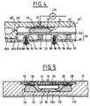
- the moldessentially consists of a fixed front part 60 and a removable rear part 62, these two parts defining the imprint for producing the body of the card. More specifically, the part 60 comprises a first planar wall 64 which defines one of the main faces of the card body and a side wall 66 which defines the edge of the card body. The second part 62 of the mold defines the second main face of the card body. The side wall 66 of the front part 60 of the mold is provided with an injection channel 68 for making the plastic material used to make the card body penetrate inside the mold. The wall 64 is provided with means for holding the electronic module 14 stationary during the injection of the plastic material into the mold.
- these meanscomprise pins such as 70 protruding from the internal face 64 of the mold, and a system for placing under vacuum comprising a suction nozzle 72 associated with a pump vacuum 74.
- the pins 70have the same spatial arrangement as the holes 36 formed in the electronic module 14.
- the suction nozzle 72opens into the part of the wall 64 limited by the pins 70.
- the manufacture of a card according to the first embodiment of the inventionis carried out in the manner following: the mold being open, the electronic module is placed in such a way that the pins 70 penetrate into the holes 36 of the metallizations 16 to 30 of the module.
- the vacuum pump 74is started.
- the module 14is therefore held against the wall 64 of the mold in the three directions and positioned by the cooperation of the pins 70 and the holes 36.
- the rear part 62 of the moldis pressed against the front part 60.
- the injection of the plastic materialthrough the injection channel 68.
- the plastic materialfills the entire cavity bounded by the mold and not occupied by the electronic module 14.
- the cardis removed from the mold.
- FIG. 5shows a partial view in vertical section of a card obtained by the implementation of the method which has just been described. It should first of all be emphasized that, due to the particular shape of the coating 50 and the production of the card body by overmolding of the electronic module, the electronic module is mechanically anchored in the card body. A very good fixing of the module is thus obtained in the card body 12. In addition, as the external face of the electronic module is pressed against the wall 64 of the mold, there is no deposit of plastic material on the pads of electrical contact 16 to 30.
- the periphery 76 of the insulating support 32 and the contact pads 16 to 30which limits the filling of the mold cavity with the plastic material, the external appearance of the card, in the connection zone between the external face of the electronic module and the corresponding face of the card body, is particularly satisfactory.
- the injection channel 68opens into a "corner" 63 of the mold defining a corner of the card body which forms a right angle while the other "corners" references 65 67 and 69 are rounded.
- the corner 63 of the card bodywhich forms a right angle
- the other "corners" references 65 67 and 69are rounded.
- FIG. 3bshows an alternative embodiment of the means for positioning and holding the electronic module in the mold.
- the wall 64 of the moldcomprises four projecting portions referenced 100 to 106 which correspond to the four corners of the insulating support of the electronic module.
- the suction nozzle 72opens into the portion of the wall 64 limited by the projecting elements 100 to 106.
- the suction nozzlecan end in a plurality of orifices 108 each corresponding to a contact area of the electronic module.
- the four portions 100 to 106one could have a complete rectangular frame projecting into the face 64 of the mold.
- the modulehas a hooking portion with the card body during the production thereof. by overmolding.
- the electronic modulecan be of the type shown in FIG. 2 but without the coating material 50.
- the attachment part of the electronic modulethen consists in all the roughness of the electronic module, including the interconnection wires 48 , which appear on the face of the electronic module not comprising the external contact pads 16, 18. It is also possible to improve the attachment properties of the electronic module with respect to the card body, for example by a surface treatment of the insulating support 32 of the module, when it exists, in its non-metallized parts.
- the module supportIt is also possible to provide holes of small dimensions in the module support, whether this support is made of insulating material or conductive material, to improve the attachment by penetration of the molding material in these holes. It is also possible to implement a physico-chemical attachment, or to combine this type of attachment with a mechanical attachment, or anchoring, of the type described above.
- the physico-chemical attachmentcan result from a judicious choice of the molding material and of the materials from which the different parts of the electronic module are made, in particular the insulating support. It is also possible to implement a chemical surface treatment of a part of the electronic module, for example the insulating support, to favor the physicochemical bonding during the molding operation.
- the expression “attachment part” of the electronic moduledoes not only designate a particular form of the covering of the module allowing it to be anchored in the card body, but all the arrangements or combinations of arrangements described above and which are intended to allow the electronic module to be secured in the card body when it is produced by molding.
- the cardhas only one electronic module.
- the moldis provided with as many fixing means (pins 70, suction nozzle 72) as there are modules, the electrical contact pads of the modules being able either to lead into one or the other. of the main faces of the card.
- FIG. 4shows a second type of mold which can be used for implementing the method according to the invention, and which makes it possible to further improve the holding in place of the electronic module during the start of the injection of the plastic material into the mold.
- the mold of Figure 4has a fixed front part 60 'which is identical to the front part 60 of the mold of Figure 3. For this reason, to designate the different elements of the front part 60', we have used the references of Figure 3 but by assigning them the sign "prime".
- the rear part of the mold 80comprises a first plate 82 whose periphery 82 ′ is intended to be pressed against the face 60′a of the front part of the mold 60 ′, and a second mobile plate 84.
- the plate 84can be moved relative to the plate 82 while being subject to remain strictly parallel to the face 64 ′ of the front part 60 ′ of the mold.
- the rear face 84 of the plate 84is provided with guide rods 86 which can slide with very little play in bearings 88 integral with the plate 82.
- the plate 84has dimensions such that its edge 84 b slides along the side wall 66 ′ of the front part 60 ′.
- Calibrated springs 90cause the spacing of the plate 84 relative to the plate 82, this spacing being limited by stops 92 integral with the rods 86.
- the fabrication of the memory card using the mold of FIG. 4is carried out as follows.
- the rear part of the mold 80being removed, the electronic module 14 is placed against the wall 64 ′ as has already been described in connection with FIG. 3.
- the rear part 80is fixed to the front part 64 ′ of the mold .
- the plate 84abuts on the face 52 of the coating 50 of the electronic module 14.
- the springs 90are chosen so that, in the position which has just been described, they are already partially compressed. The prestressing of the springs 90 further improves the way in which the electronic module is held pressed against the wall 64 ′ of the mold.
- the plastic materialis introduced into the mold through the injection channel 68 ′.
- a first phasedue to the preload of the springs 90, the plate 84 remains stationary in abutment on the surface 52 of the module and the plastic material fills the space surrounding the module 14 and limited by the plate 84 and the front part of the mold 60 ′.
- This phaselasts until the pressure of the plastic material compensates for the preload of the springs 90 Then the plastic material gradually pushes back the plate 84 by compressing the springs 90, the plate 84 no longer being in contact with the module 14. However the plastic material then surrounds completely the electronic module 14 which contributes to keeping it in place against the wall 64 ′.
- the tray 84is pushed back by the plastic material until it comes into contact with mechanical stops 96 integral with the tray 82.
- the plastic material which is used for the production of the card body by moldingcan be an acrylonitryl-butadiene-styrene or any other similar type of plastic material.
- the materialis injected at a temperature between 180 C and 280 C and preferably between 220 and 260 C, and the mold is maintained at a temperature between 5 and 100 C preferably between 10 and 50 C.
- Polystyrene, polypropylene and polyamine 11can also be used as thermoplastic material.
- a magnetic strip 112can be fixed on the rear face 110 of the card body, for example by hot pressing.
- the embodiment of the card body according to the inventionlends itself particularly well to the installation of this track.
- the portion 12b of the card body disposed between the electronic module and the rear face 110 of the card bodyhas great stability despite its reduced thickness because this portion is directly molded onto the face 52 of the card body. electronic module.
- the material usedlends itself very well to writing by embossing information on one of the main faces of the card body.
- FIG. 6there is shown the front part 160 of the mold which includes all of the imprints.
- the part 160 of the moldhas 4 cavities 162, 164, 166 and 168 which define the bodies of the four cards produced simultaneously.
- an electronic module 14In each imprint 162 to 168 is placed an electronic module 14 according to one of the techniques described in conjunction with Figures 3 to 3b.
- the footprints 162 to 168are separated from one another by projecting parts 170 to 176. As shown in FIG. 6, the projecting parts 170 to 176 do not completely separate the footprints from each other, but passages make communicate the footprints between them.
- the passages 178 to 186have a depth less than that of the imprints 162 to 168. It goes without saying that these passages could have the same depth as the imprints.
- the injection of the material into the moldcan be done in two ways: either the injection is carried out at several points 188 to 194, each injection point opening into one of the passages 178 to 186; either the sheet is injected through the lateral opening 196 which opens into the passage 182.
Landscapes
- Engineering & Computer Science (AREA)
- General Physics & Mathematics (AREA)
- Computer Hardware Design (AREA)
- Microelectronics & Electronic Packaging (AREA)
- Physics & Mathematics (AREA)
- Theoretical Computer Science (AREA)
- Manufacturing & Machinery (AREA)
- Mechanical Engineering (AREA)
- Condensed Matter Physics & Semiconductors (AREA)
- Power Engineering (AREA)
- Credit Cards Or The Like (AREA)
- Holo Graphy (AREA)
- Packaging For Recording Disks (AREA)
- External Artificial Organs (AREA)
- Electrically Operated Instructional Devices (AREA)
- Devices For Indicating Variable Information By Combining Individual Elements (AREA)
- Injection Moulding Of Plastics Or The Like (AREA)
- Non-Volatile Memory (AREA)
- Collating Specific Patterns (AREA)
- Compression, Expansion, Code Conversion, And Decoders (AREA)
- Diaphragms For Electromechanical Transducers (AREA)
Abstract
Description
Translated fromFrenchLa présente invention concerne un procédé de réalisation de cartes à mémoire notamment électronique et des cartes obtenues par la mise en oeuvre dudit procédé.The present invention relates to a method for producing memory cards, in particular electronic cards, and to cards obtained by implementing said method.
Les cartes à mémoire comprennent essentiellement un corps de carte qui est réalisé en général en un matériau plastique et un module mémoire.Dans le cas des cartes à mémoire électronique le module mémoire est un module électronique comportant essentiellement une pastille semi-conductrice ou "chip" dans laquelle est réalisé un circuit intégré et un élément de circuit imprimé sur lequel est fixé le chip et qui définit des plages externes de contact électrique. Le module électronique est fixé dans le corps de la carte de telle manière que les plages de contact électrique affleurent une des faces principales du corps de carte.Memory cards essentially comprise a card body which is generally made of a plastic material and a memory module. In the case of electronic memory cards the memory module is an electronic module essentially comprising a semiconductor chip or "chip" in which an integrated circuit and a printed circuit element on which the chip is fixed and which defines external electrical contact pads are produced. The electronic module is fixed in the body of the card in such a way that the electrical contact pads are flush with one of the main faces of the card body.
Le corps de carte a la forme d'un parallèlèpipède rectangle dont l'épaisseur est réduite comparée aux autres dimensions du corps de carte. Les bords du corps de carte servent de référence pour le positionnement de la carte dans le lecteur de cartes de telle manière que les plages de contact de la carte viennent en contact électrique avec le connecteur du lecteur de cartes.The card body has the shape of a rectangular parallelepiped whose thickness is reduced compared to the other dimensions of the card body. The edges of the card body serve as a reference for positioning the card in the card reader so that the contact areas of the card come into electrical contact with the connector of the card reader.
Deux techniques principales sont utilisées actuellement pour réaliser le corps de carte et l'implantation du module électronique dans le corps de carte. Selon une première technique, le corps de carte est réalisé par laminage à chaud de plusieurs feuilles de matériau plastique tel que de PVC. Le module électronique est mis en place dans l'empilement de feuilles de matériau plastique avant le laminage. Après l'opération de laminage, le module électronique est solidement ancré dans le corps de la carte. Ce procédé présente l'avantage de réaliser en une seule étape le corps de carte et l'implantation du module électronique dans le corps de carte. En revanche ce procédé est délicat et il nécessite le réusinage de la périphérie du corps de carte.Two main techniques are currently used to produce the card body and the implantation of the electronic module in the card body. According to one first technique, the card body is produced by hot rolling several sheets of plastic material such as PVC. The electronic module is placed in the stack of sheets of plastic material before rolling. After the laminating operation, the electronic module is firmly anchored in the body of the card. This method has the advantage of producing the card body in one step and the implantation of the electronic module in the card body. On the other hand, this process is delicate and it requires re-machining of the periphery of the card body.
La deuxième technique consiste à réaliser le corps de carte dans une première étape, à usiner une cavité dans le corps de carte pour recevoir le module électronique et à coller le module électronique dans la cavité. L'usinage d'un tel corps de carte est toujours une opération délicate, donc onéreuse, car des cotes très précises doivent être respectées notamment pour assurer un positionnement correct du module électronique par rapport aux bords de la carte et par rapport à la face principale du corps de carte dans laquelle doivent affleurer les plages de contact électrique. De plus la fixation du module électronique dans le corps de carte ajoute des étapes supplémentaires, par exemple le collage.The second technique consists in making the card body in a first step, in machining a cavity in the card body to receive the electronic module and in bonding the electronic module in the cavity. The machining of such a card body is always a delicate operation, therefore expensive, because very precise dimensions must be respected in particular to ensure correct positioning of the electronic module with respect to the edges of the card and with respect to the main face. of the card body in which the electrical contact pads must be flush. In addition fixing the electronic module in the card body adds additional steps, for example bonding.
Il faut ajouter que le corps de carte doit en outre répondre à d'autres spécifications concernant la qualité de l'état de surface et les propriétés de tenue en flextion bien précises ausi bien selon la direction longitudinale du corps de carte que selon sa direction transversale. De plus il faut que le corps de carte ne favorise pas le stockage de charges électrostatiques. Un objet de la présente invention est de fournir un procédé de réalisation de cartes à mémoire notamment à mémoire électronique qui permettre d'abaisser le coût de fabrication du corps de carte et qui réalise simultanément l'opération de fixation du module électronique dans le corps de carte, tout en répondant aux spécifications énoncées ci-dessus.It should be added that the card body must also meet other specifications concerning the quality of the surface condition and the very precise flexural strength properties as well in the longitudinal direction of the card body as in its transverse direction. . In addition, the card body must not favor the storage of electrostatic charges. An object of the present invention is to provide a method of making memory cards, in particular to electronic memory which makes it possible to lower the manufacturing cost of the card body and which simultaneously performs the operation of fixing the electronic module in the card body, while meeting the specifications set out above.
Le document EP-A-0 246 973, publié le 25 novembre 1987, décrit un procédé de réalisation de carte à élément électronique qui vise à obtenir une carte présentant un corps renforcé par un socle métallique. Les documents JP-A-60/146383 et JP-A-60/86850 décrivent des procédés de réalisation de cartes à mémoire électronique par moulage à l'aide d'une résine durcissable par un faisceau d'électrons ou par un rayonnement lumineux.The document EP-A-0 246 973, published on November 25, 1987, describes a method for producing a card with an electronic element which aims to obtain a card having a body reinforced by a metal base. The documents JP-A-60/146383 and JP-A-60/86850 describe methods for producing electronic memory cards by molding using a resin curable by an electron beam or by light radiation.
Pour atteindre ce but, selon l'invention, le procédé de réalisation d'une carte à mémoire électronique comprenant un module mémoire électronique comportant des plages de contact externes, une pastille semi-conductrice solidaire de la face postérieure desdits contacts, des moyens d'interconnexion des bornes de ladite pastille aux plages de contact et un matériau d'enrobage de ladite pastille et un corps de carte, caractérisé en ce qu'il comprend les étapes suivantes :
on fournit un module mémoire électronique comportant en outre une partie d'accrochage destinée à la fixation dudit module dans le corps de la carte par un engagement positif de forme et/ou par accrochage physico-chimique;
on place ledit module mémoire électronique dans un moule d'injection dont la cavité interne définit la forme du corps de carte et on maintient le module électronique de telle manière que les plages de contact externe soient plaquées contre une paroi de ladite cavité à l'aide de moyens solidaires dudit moule ;
on injecte à chaud et sous pression dans la cavité dudit moule un matériau thermo-plastique choisi dans le groupe comprenant l'acrylonitryl-butadiène-styrène, le polystyrène, le propylène et le polyamine 11, de telle manière que ledit matériau plastique remplisse la totalité de la cavité non occupée par ledit module, et
on démoule la pièce ainsi réalisée.To achieve this object, according to the invention, the method of producing an electronic memory card comprising an electronic memory module comprising external contact pads, a semiconductor patch secured to the rear face of said contacts, means of interconnection of the terminals of said pad to the contact pads and a coating material of said pad and a card body, characterized in that it comprises the following steps:
an electronic memory module is provided, further comprising a hooking part intended for fixing said module in the body of the card by a positive shape engagement and / or by physicochemical hooking;
said electronic memory module is placed in an injection mold whose internal cavity defines the shape of the card body and the electronic module is maintained in such a way that the external contact pads are pressed against a wall of said cavity using solidarity means of said mold;
a thermo-plastic material chosen from the group comprising acrylonitryl-butadiene-styrene, polystyrene, propylene and polyamine 11 is injected hot and under pressure into the cavity of said mold, so that said plastic material fills the whole of the cavity not occupied by said module, and
the part thus produced is removed from the mold.
On comprend que, selon l'invention, le corps de la carte est directement réalisé par surmoulage du module mémoire. En une seule étape, on fabrique le corps de carte et on réalise l'implantation du module dans le corps. De plus le module pouvant être positionné dans le moule avec une grande précision, le module est également positionné avec une grande précision dans le corps de carte.It is understood that, according to the invention, the body of the card is directly produced by overmolding the memory module. In a single step, the card body is manufactured and the module is implanted in the body. In addition, the module can be positioned in the mold with great precision, the module is also positioned with great precision in the card body.
L'invention sera mieux comprise à la lecture de la description qui suit de plusieurs modes de mise en oeuvre de l'invention donnés à titre d'exemples non limitatifs. La description se réfère au dessins annexé sur lequel :
- La figure 1 est une vue de dessus d'une carte à mémoire électronique conforme à l'invention ;
- La figure 2 est une vue en coupe verticale d'un module électronique utilisable dans l'invention ;
- La figure 3 est une vue simplifiée en coupe d'un premier type de moule pour la mise en oeuvre de l'invention ;
- La figure 3a est une vue en coupe selon la ligne A-A de la figure 3, montrant une première variante du moule de la figure 3;
- La figure 3b est une vue en coupe selon la ligne A-A de la figure 3, montrant une deuxième variante du moule de la figure 3;
- La figure 4 est une vue simplifiée en coupe d'un deuxième type de moule pour la mise en oeuvre de l'invention ;
- La figure 5 est une vue partielle en coupe verticale d'une carte à mémoire électronique conforme à l'invention.
- La figure 6 est une vue de dessus d'un troisième type de moule permettant de réaliser simultanément plusieurs cartes ; et
- La figure 7 est une vue en coupe verticale selon la ligne VII-VII de la figure 6.
- Figure 1 is a top view of an electronic memory card according to the invention;
- Figure 2 is a vertical sectional view of an electronic module usable in the invention;
- Figure 3 is a simplified sectional view of a first type of mold for the implementation of the invention;
- Figure 3a is a sectional view along line AA of Figure 3, showing a first variant of the mold of Figure 3;
- Figure 3b is a sectional view along line AA of Figure 3, showing a second variant of the mold of Figure 3;
- Figure 4 is a simplified sectional view of a second type of mold for the implementation of the invention;
- Figure 5 is a partial view in vertical section of an electronic memory card according to the invention.
- Figure 6 is a top view of a third type of mold for making several cards simultaneously; and
- FIG. 7 is a view in vertical section along the line VII-VII of FIG. 6.
La figure 1 montre en vue de dessus une partie d'une carte à mémoire électronique 10. La carte 10 comporte un corps 12 réalisé en un matériau plastique et un module électronique 14 dont la figure 1 ne montre que des plages externes de contact électrique 16 à 30 disposées sur un support isolant 32. Comme cela est bien connu les plages de contact 16 à 30 sont destinées à entrer en contact électrique avec le connecteur des lecteurs de cartes utilisés pour fonctionner avec les cartes.Figure 1 shows a top view of a part of an
La figure 2 montre un module électronique 14 bien adapté pour la mise en oeuvre de l'invention. Le module 14 comprend un support isolant 32 sur la face 32ª duquel sont réalisées les plages externes de contact électrique. La figure 2 montre les plages 18, 28 et 16. Les plages de contact sont séparées les unes des autres par des zones gravées telles que 34. Les plages de contact et le support isolant 32 comportent de plus une série de trous tels que 36 dont la fonction sera explicitée ultérieurement. La deuxième face 32b du support isolant 32 comporte également des métallisations 38, 40.FIG. 2 shows an
Une pastille semi-conductrice 42 est fixée sur la métallisation centrale 38 à l'aide d'un matériau adhésif conducteur. La métallisation 38 et les métallisations 40 sont électriquement reliées aux plages de contact 16 à 30 à travers des trous 44 ménagés dans le support isolant 32. En outre chaque borne 46 de la pastille semi-conductrice 42 est reliée à une métallisation 40 par un fil conducteur 48.A
La pastille 42 et les fils 48 sont noyés dans un matériau d'enrobage isolant 50 qui adhère fortement aux métallisations 40 à la pastille 42 et aux fils 48. Il s'agit par exemple d'une résine thermodurcissable . De plus le matériau d'enrobage 50 est moulé ou usiné pour présenter un fond 52 sensiblement plat et parallèle au support isolant 32. La paroi latérale 54 du matériau d'enrobage est inclinée est fait un angle ª inférieur à 90° avec la portion non recouverte par le matériau d'enrobage de la face 32b du support isolant 32.The
En se référant maintenant à la figure 3 on va décrire un premier mode, selon l'invention, de réalisation du corps de carte et de fixation du module électronique dans le corps de carte. Le moule est constitué essentiellement par une partie avant fixe 60 et par une partie arrière amovible 62, ces deux parties définissant l'empreinte pour réaliser le corps de la carte. Plus précisément la partie 60 comporte une première paroi plane 64 qui définit une des faces principales du corps de carte et une paroi latérale 66 qui définit la tranche du corps de carte. La deuxième partie 62 du moule définit la deuxième face principale du corps de carte. La paroi latérale 66 de la partie avant 60 du moule est munie d'un canal d'injection 68 pour faire pénétrer à l'intérieur du moule le matériau plastique servant à réaliser le corps de carte. La paroi 64 est munie de moyens pour maintenir immobile le module électronique 14 lors de l'injection du matériau plastique dans le moule. Selon ce premier mode de mise en oeuvre de l'invention, ces moyens comprennent des picots tels que 70 faisant saillie hors de la face interne 64 du moule, et un système de mis en dépression comportant un ajutage d'aspiration 72 associé à une pompe à vide 74. Les picots 70 présentent la même disposition spatiale que les trous 36 ménagés dans le module électronique 14. De plus l'ajutage d'aspiration 72 débouche dans la partie de la paroi 64 limitée par les picots 70.Referring now to Figure 3 we will describe a first embodiment, according to the invention, of the card body and fixing the electronic module in the card body. The mold essentially consists of a fixed
La fabrication d'une carte selon le premier mode de mise en oeuvre de l'invention est réalisée de la manière suivante : le moule étant ouvert, le module électronique est mis en place de telle manière que les picots 70 pénêtrent dans les trous 36 des métallisations 16 à 30 du module. La pompe à vide 74 est mise en route. Le module 14 est donc maintenu contre la paroi 64 du moule dans les trois directions et positionné par la coopération des picots 70 et des trous 36. La partie arrière 62 du moule est plaquée sur la partie avant 60. On commande alors l'injection du matériau plastique par le canal d'injection 68. Le matériau plastique remplit l'ensemble de la cavité limitée par le moule et non occupée par le module électronique 14. On procède ensuite au démoulage de la carte.The manufacture of a card according to the first embodiment of the invention is carried out in the manner following: the mold being open, the electronic module is placed in such a way that the
La figure 5 montre une vue partielle en coupe verticale d'une carte obtenue par la mise en oeuvre du procédé qui vent d'être décrit. Il faut souligner tout d'abord que, en raison de la forme particulière de l'enrobage 50 et de la réalisation du corps de carte par surmoulage du module électronique , le module électronique est mécaniquement ancré dans le corps de carte. On obtient ainsi une très bonne fixation du module dans le corps de carte 12. En outre, comme la face externe du module électronique est plaquée contre la paroi 64 du moule, il n'y a pas de dépôt de matériau plastique sur les plages de contact électrique 16 à 30. De plus, comme c'est la périphérie 76 du support isolant 32 et des plages de contact 16 à 30 qui limite le remplissage de la cavité du moule par le matériau plastique, l'aspect extérieur de la carte, dans la zone de liaison entre la face externe du module électronique et la face correspondante du corps de carte, est particulièrement satisfaisant.FIG. 5 shows a partial view in vertical section of a card obtained by the implementation of the method which has just been described. It should first of all be emphasized that, due to the particular shape of the
De préférence, comme le montre la figure 3a, le canal d'injection 68 débouche dans un "coin" 63 du moule définissant un coin du corps de carte qui forme un angle droit alors que les autres "coins" références 65 67 et 69 sont arrondis. Ainsi, après découpage du coin 63 du corps de carte toute trace éventuelle d'injection disparait. Il est possible de prévoir plusieurs canaux d'injection débouchant chacun dans un "coin" du moule.Preferably, as shown in FIG. 3a, the
La figure 3b montre une variante de réalisation des moyens de positionnement et de maintien du module électronique dans le moule. Au lieu ou en plus des picots 70, la paroi 64 du moule comprend quatre portions en saillie référencées 100 à 106 qui correspondent aux quatre coins du support isolant du module électronique. L'ajutage d'aspiration 72 débouche dans la portion de la paroi 64 limitée par les éléments en saillie 100 à 106. Comme le montre la figure 3b l'ajutage d'aspiration peut se terminer par une pluralité d'orifices 108 correspondant chacun à une plage de contact du module électronique. Au lieu des quatre portions 100 à 106 on pourrait avoir un cadre rectangulaire complet faisant saillie dans la face 64 du moule.FIG. 3b shows an alternative embodiment of the means for positioning and holding the electronic module in the mold. Instead of or in addition to the
Il va de soi qu'on pourrait utiliser d'autres types de module électronique. Par exemple des modules électroniques du type décrit dans les demandes de brevet français 2.547.440, 2.555.780 ou 2.579.799. Il peut encore s'agir d'un module électronique du type à "lead-frame". De tels modules électroniques sont décrits dans la demande de brevet européen Nr 87/401697 déposée le 21 juillet 1987. Un tel module ne comporte pas de support isolant. La pastille semi conductrice est directement fixée sur un élément conducteur formant une des plages de contact de la carte à mémoire et les bornes de la pastille sont reliées par des fils conducteurs à d'autres éléments conducteurs qui forment les autres plages de connexion de la carte.It goes without saying that other types of electronic module could be used. For example electronic modules of the type described in French patent applications 2,547,440, 2,555,780 or 2,579,799. It can also be an electronic module of the "lead-frame" type. Such electronic modules are described in European patent application Nr 87/401697 filed on July 21, 1987. Such a module does not include an insulating support. The semiconductor patch is directly fixed on a conductive element forming one of the contact areas of the memory card and the terminals of the patch are connected by conductive wires to other conductive elements which form the others. card connection areas.
Au lieu que le module électronique présente un élément d'ancrage tel que la forme externe particulière de l'enrobage du chip, il est possible que le module présente une partie d'accrochage avec le corps de carte lors de la réalisation de celui-ci par surmoulage. Par exemple, le module électronique peut être de type représenté sur la figure 2 mais sans le matériau d'enrobage 50. La partie d'accrochage du module électronique consiste alors dans toutes les aspérités du modules électronique, y compris les fils 48 d'interconnexion, qui apparaissent sur la face du module électronique ne comportant pas les plages de contact externes 16, 18. Il est également possible d'améliorer les propriétés d'accrochage du module électronique vis-à-vis du corps de carte, par exemple par un traitement de surface du support isolant 32 du module, lorsqu'il existe, dans ses parties non métallisées. Il est encore possible de prévoir des perçages de petites dimensions dans le support de module, que ce support soit en matériau isolant ou en matériau conducteur, pour améliorer l'accrochage par pénétration du matériau de moulage dans ces perçages. Il est encore possible de mettre en oeuvre un accrochage physico-chimique, ou de combiner ce type d'accrochage avec un accrochage mécanique, ou ancrage, du type décrit précédemment. L'accrochage physico-chimique peut résulter d'un choix judicieux du matériau de moulage et des matériaux dont sont faites les différentes parties du module électronique, notamment le support isolant. Il est également possible de mettre en oeuvre un traitement de surface chimique d'une partie du module électronique, par exemple le support isolant, pour favoriser l'accrochage physico-chimique lors de l'opération de moulage.Instead of the electronic module having an anchoring element such as the particular external shape of the coating of the chip, it is possible that the module has a hooking portion with the card body during the production thereof. by overmolding. For example, the electronic module can be of the type shown in FIG. 2 but without the
On voit que dans la présente demande de brevet, l'expression "partie d'accrochage" du module électronique ne désigne pas uniquement une forme particulière de l'enrobage du module permettant l'ancrage de celui-ci dans le corps de carte, mais toutes les dispositions ou combinaisons de dispositions décrites ci-dessus et qui visent à permettre la solidarisation du module électronique dans le corps de carte lors de la réalisation de celui-ci par moulage.It can be seen that in the present patent application, the expression “attachment part” of the electronic module does not only designate a particular form of the covering of the module allowing it to be anchored in the card body, but all the arrangements or combinations of arrangements described above and which are intended to allow the electronic module to be secured in the card body when it is produced by molding.
Dans la description précédente la carte ne comporte qu'un seul module électronique. On pourrait à l'aide du procédé de l'invention réaliser une carte ayant plusieurs modules indépendants. Dans ce cas le moule est muni d'autant de moyens de fixation (picots 70, Ajutage d'aspiration 72) qu'il y a de modules, les plages de contact électrique des modules pouvant indifféremment déboucher dans l'une ou l'autre des faces principales de la carte. La figure 4 montre un deuxième type de moule qui peut être utilisé pour la mise en oeuvre de procédé selon l'invention, et qui permet d'améliorer encore le maintien en place du module électronique lors du début de l'injection du matériau plastique dans le moule.In the preceding description, the card has only one electronic module. Using the method of the invention, it would be possible to produce a card having several independent modules. In this case, the mold is provided with as many fixing means (pins 70, suction nozzle 72) as there are modules, the electrical contact pads of the modules being able either to lead into one or the other. of the main faces of the card. FIG. 4 shows a second type of mold which can be used for implementing the method according to the invention, and which makes it possible to further improve the holding in place of the electronic module during the start of the injection of the plastic material into the mold.
Le moule de la figure 4 comporte une partie avant fixe 60′ qui est identique à la partie avant 60 du moule de la figure 3. Pour cette raison, pour désigner les différents éléments de la partie avant 60′, on a repris les références de la figure 3 mais en les affectant du signe "prime". La partie arrière du moule 80 comprend un premier plateau 82 dont la périphérie 82ª est destinée à être plaquée sur la face 60′a de la partie avant du moule 60′, et un deuxième plateau mobile 84. Le plateau 84 peut être déplacé par rapport au plateau 82 en étant assujetti à rester rigoureusement parallèle à la face 64′ de la partie avant 60′ du moule. Pour cela la face arrière 84ª du plateau 84 est munie de tiges de guidage 86 qui peuvent coulisser avec un jeu très réduit dans des paliers 88 solidaires du plateau 82. Le plateau 84 a des dimensions telles que sa tranche 84b glisse le long de la paroi latérale 66′ de la partie avant 60′. Des ressorts tarés 90 provoquent l'écartement du plateau 84 par rapport au plateau 82, cet écartement étant limité par des butées 92 solidaires des tiges 86.The mold of Figure 4 has a fixed front part 60 'which is identical to the
La fabrication de la carte à mémoire à l'aide du moule de la figure 4 est réalisée de la manière suivante. La partie arrière du moule 80 étant enlevée, le module électronique 14 est mis en place contre la paroi 64′ comme cela a déjà été décrit en liaison avec la figure 3. Puis la partie arrière 80 est fixée sur la partie avant 64′ du moule. Le plateau 84 vient en butée sur la face 52 de l'enrobage 50 du module électronique 14. Les ressorts 90 sont choisis de telle manière que, dans la position qui vient d'être décrite, ils soient déjà partiellement comprimés. La précontrainte des ressorts 90 améliore encore la façon dont le module électronique est maintenu plaqué contre la paroi 64′ du moule. Puis on commande l'introduction du matériau plastique dans le moule par le canal d'injection 68′. Dans une première phase, en raison de la précontrainte des ressorts 90 , le plateau 84 reste immobile en appui sur la surface 52 du module et le matériau plastique remplit l'espace entourant le module 14 et limité par le plateau 84 et la partie avant du moule 60′. Cette phase dure jusqu'à ce que la pression du matériau plastique compense la précontrainte des ressorts 90 Puis le matériau plastique repousse progressivement le plateau 84 en comprimant les ressorts 90, le plateau 84 n'étant plus en contact avec le module 14. Cependant le matériau plastique entoure alors complétement le module électronique 14 ce qui participe à son maintien en place contre la paroi 64′. Le plateau 84 est repoussé par le matériau plastique jusqu'à ce qu'il arrive en contact avec des butées mécaniques 96 solidaires du plateau 82. Cette position est déterminée pour que le corps de carte ainsi obtenu ait l'épaisseur requise compte tenu du retrait. L'injection est alors arrêtée, la partie arrière 82 enlevée et la carte extraite du moule. On obtient ainsi une carte identique à celle qui est représentée sur la figure 5. Il va de soi que le moule de la figure 4 peut comporter les variantes illustrées par les figures 3a et 3b.The fabrication of the memory card using the mold of FIG. 4 is carried out as follows. The rear part of the
Le matériau plastique qui est utilisé pour la réalisation du corps de carte par moulage peut être un acrylonitryl-butadiène-styrène ou tout autre type de matériau plastique similaire. Dans le cas de l′A.B.S., le matériau est injecté à une température comprise entre 180 C et 280 C et de préférence entre 220 et 260 C, et le moule est maintenu à une température comprise entre 5 et 100 C de préférence entre 10 et 50 C.The plastic material which is used for the production of the card body by molding can be an acrylonitryl-butadiene-styrene or any other similar type of plastic material. In the case of ABS, the material is injected at a temperature between 180 C and 280 C and preferably between 220 and 260 C, and the mold is maintained at a temperature between 5 and 100 C preferably between 10 and 50 C.
On peut également utiliser comme matériau thermoplastique le polystyrène, le polypropylène et le polyamine 11.Polystyrene, polypropylene and polyamine 11 can also be used as thermoplastic material.
Comme le montre la figure 5 on peut fixer sur la face arrière 110 du corps de carte une piste magnétique 112 par exemple par pressage à chaud. Il faut souligner que le mode de réalisation du corps de carte selon l'invention se prête particuliairement bien à la mise en place de cette piste. En effet la portion 12b du corps de carte disposée entre le module électronique et la face arrière 110 du corps de carte présente une grande stabilité malgrè son épaisseur réduite du fait que cette portion est directement surmoulée sur la face 52 du module électronique. En outre le matériau utilisé se prête très bien à l'inscription par embossage d'informations sur une des faces principales du corps de carte.As shown in FIG. 5, a
En se référant aux figures 6 et 7 on va décrire un mode de réalisation du moule qui permet d'obtenir simultanément plusieurs cartes.Referring to Figures 6 and 7 we will describe an embodiment of the mold which allows to obtain several cards simultaneously.
Sur la figure 6 on a représenté la partie avant 160 du moule qui comporte l'ensemble des empreintes. La partie 160 du moule comporte 4 empreintes 162, 164, 166 et 168 qui définissent les corps des quatre cartes fabriquées simultanément. Dans chaque empreinte 162 à 168 est mis en place un module électronique 14 selon une des techniques décrites en liaison avec les figures 3 à 3b. Les empreintes 162 à 168 sont séparées les unes des autres par des parties en saillie 170 à 176. Comme le montre la figure 6, les parties en saillie 170 à 176 ne séparent pas totalement les empreintes les unes des autres, mais des passages font communiquer les empreintes entre elles. On trouve un passage central 178 qui fait communiquer les quatres empreintes, et des passages d'extrémité 180 à 186 qui font communiquer les empreintes deux à deux à proximité de la périphérie de la partie avant 160 du moule. Comme le montre la figure 7, les passages 178 à 186 ont une profondeur inférieure à celle des empreintes 162 à 168. Il va de soi que ces passages pourraient avoir la même profondeur que les empreintes. L'injection de la matière dans le moule peut se faire de deux manières : soit on effectue l'injection en plusieurs points 188 à 194, chaque point d'injection débouchant dans un des passages 178 à 186 ; soit on effectue l'injection en nappe par l'ouverture latérale 196 qui débouche dans le passage 182.In Figure 6 there is shown the
Après démoulage on obtient une pièce unique qui consiste en quatre cartes, correspondant aux empreintes 162 à 168, reliées entre elles par des "points" correspondant au matériau plastique qui a rempli les passages 178 à 186.After removal from the mold, a single piece is obtained which consists of four cards, corresponding to the
Le fait d'obtenir quatre cartes reliées mécaniquement entre elles avec des positionnements relatifs très précis des cartes, est très avantageux pour effectuer ultérieurement l'impression par offset du corps de carte. En effet, d'une part l'impression peut se faire simultanément, d'autre part la pièce ayant des dimensions plus importantes il est plus facile de la positionner sur la machine d'impression.The fact of obtaining four cards mechanically linked together with very precise relative positions of the cards is very advantageous for subsequently performing offset printing of the card body. Indeed, on the one hand the printing can be done simultaneously, on the other hand the part having larger dimensions it is easier to position it on the printing machine.
Pour séparer les cartes les unes des autres, il suffit de découper les "points". Cette opération ne présente aucune difficulté particulière puisque les "points" sont attachés aux corps de carte à un de leurs "coins", il s'agit donc d'une partie non fonctionnelle du corps de carte. En outre, les points d'injection 188 à 196 débouchant dans ces "points", les traces d'injection sont éliminées en même temps que les "points".To separate the cards from each other, simply cut out the "dots". This operation does not present any particular difficulty since the "points" are attached to the card bodies at one of their "corners", it is therefore a non-functional part of the card body. In addition, the injection points 188 to 196 opening into these "points", the injection traces are eliminated at the same time as the "points".
Claims (12)
Priority Applications (1)
| Application Number | Priority Date | Filing Date | Title |
|---|---|---|---|
| AT88400068TATE74456T1 (en) | 1987-01-16 | 1988-01-14 | MANUFACTURING PROCESS FOR MEMORY CARDS AND CARDS OBTAINED BY THIS PROCESS. |
Applications Claiming Priority (2)
| Application Number | Priority Date | Filing Date | Title |
|---|---|---|---|
| FR8700446AFR2609821B1 (en) | 1987-01-16 | 1987-01-16 | METHOD FOR REALIZING MEMORY CARDS AND CARDS OBTAINED BY THE IMPLEMENTATION OF SAID METHOD |
| FR8700446 | 1987-01-16 |
Publications (2)
| Publication Number | Publication Date |
|---|---|
| EP0277854A1 EP0277854A1 (en) | 1988-08-10 |
| EP0277854B1true EP0277854B1 (en) | 1992-04-01 |
Family
ID=9346968
Family Applications (1)
| Application Number | Title | Priority Date | Filing Date |
|---|---|---|---|
| EP88400068AExpired - LifetimeEP0277854B1 (en) | 1987-01-16 | 1988-01-14 | Memory card manufacturing process and cards obtained by this process |
Country Status (18)
| Country | Link |
|---|---|
| EP (1) | EP0277854B1 (en) |
| JP (1) | JPS63239097A (en) |
| KR (1) | KR880009317A (en) |
| AT (1) | ATE74456T1 (en) |
| AU (1) | AU600785B2 (en) |
| BR (1) | BR8800135A (en) |
| CA (1) | CA1306058C (en) |
| DE (1) | DE3869635D1 (en) |
| DK (1) | DK16988A (en) |
| ES (1) | ES2031248T3 (en) |
| FI (1) | FI93156C (en) |
| FR (1) | FR2609821B1 (en) |
| GR (1) | GR3004900T3 (en) |
| IN (1) | IN170183B (en) |
| NO (1) | NO178089C (en) |
| NZ (1) | NZ223192A (en) |
| PT (1) | PT86557A (en) |
| ZA (1) | ZA88279B (en) |
Cited By (18)
| Publication number | Priority date | Publication date | Assignee | Title |
|---|---|---|---|---|
| FR2622323A1 (en)* | 1987-10-22 | 1989-04-28 | Nippon Eurotec | Card intended to serve as a substrate for memory cards |
| EP0340099A1 (en)* | 1988-04-28 | 1989-11-02 | Schlumberger Industries | Manufacturing process for memory cards comprising graphic elements, and cards obtained by this process |
| FR2636755A1 (en)* | 1988-09-16 | 1990-03-23 | Schlumberger Ind Sa | Method of producing memory cards and cards obtained by the said method |
| EP0326822A3 (en)* | 1988-02-01 | 1990-05-30 | Motorola Inc. | Data device module |
| FR2647571A1 (en)* | 1989-05-26 | 1990-11-30 | Lemaire Gerard | Method of fabricating a card known as a chip card, and card obtained by this method |
| EP0412893A1 (en)* | 1989-08-07 | 1991-02-13 | Schlumberger Industries | Method for making card bodies and cards with graphic elements and card bodies so obtained |
| EP0390996A3 (en)* | 1989-04-06 | 1991-03-06 | Mitsubishi Denki Kabushiki Kaisha | Ic card module |
| EP0361194A3 (en)* | 1988-09-30 | 1991-06-12 | Siemens Aktiengesellschaft | Method of enveloping electrical or electronic components or component assemblies, and envelope for electrical or electronic components or component assemblies |
| EP0377937A3 (en)* | 1989-01-12 | 1991-07-03 | Mitsubishi Denki Kabushiki Kaisha | Ic card |
| FR2659157A2 (en)* | 1989-05-26 | 1991-09-06 | Lemaire Gerard | METHOD FOR MANUFACTURING A CARD, SAID CARD, AND CARD OBTAINED BY THIS PROCESS. |
| FR2666687A1 (en)* | 1990-09-06 | 1992-03-13 | Sgs Thomson Microelectronics | INTEGRATED CIRCUIT WITH MOLDED CASE COMPRISING A THERMAL DISSIPATOR AND MANUFACTURING METHOD. |
| EP0480197A1 (en)* | 1990-10-09 | 1992-04-15 | STMicroelectronics S.r.l. | A method for manufacturing plastics IC packages incorporating a heat sink |
| US5286426A (en)* | 1992-04-01 | 1994-02-15 | Allegro Microsystems, Inc. | Assembling a lead frame between a pair of molding cavity plates |
| US5350553A (en)* | 1990-11-27 | 1994-09-27 | Mannesmann Aktiengesellschaft A Corp Of The Federal Republic Of Germany | Method for the manufacture of a decorated chip card |
| EP0709805A2 (en) | 1994-10-06 | 1996-05-01 | Giesecke & Devrient GmbH | Method for producing data carriers with embedded elements and device for carrying out this method |
| US5888624A (en)* | 1994-02-04 | 1999-03-30 | Giesecke & Devrient Gmbh | Data carrier with an electronic module and a method for producing the same |
| US5935497A (en)* | 1995-06-21 | 1999-08-10 | Schlumberger Industries | Method of printing a graphic on a memory card |
| US6614100B1 (en) | 1996-06-24 | 2003-09-02 | Infineon Technologies Ag | Lead frame for the installation of an integrated circuit in an injection-molded package |
Families Citing this family (19)
| Publication number | Priority date | Publication date | Assignee | Title |
|---|---|---|---|---|
| US5244840A (en)* | 1989-05-23 | 1993-09-14 | Mitsubishi Denki Kabushiki Kaisha | Method for manufacturing an encapsulated IC card having a molded frame and a circuit board |
| FI913357L (en)* | 1991-07-10 | 1993-01-11 | Valtion Teknillinen | FOERFARANDE OCH FORM FOER FRAMSTAELLNING AV EN STRAENGSPRUTAD ELEKTRONIKMODUL |
| DE4401588C2 (en)* | 1994-01-20 | 2003-02-20 | Gemplus Gmbh | Method for capping a chip card module and chip card module |
| JPH0890600A (en)* | 1994-09-22 | 1996-04-09 | Rhythm Watch Co Ltd | Ic card manufacturing mold |
| JP3409943B2 (en)* | 1995-05-25 | 2003-05-26 | 昭和電工株式会社 | Plug for infusion container and method for producing the same |
| EP0890928A3 (en)* | 1997-07-10 | 2001-06-13 | Sarnoff Corporation | Transmission apparatus and remotely identifying an electronically coded article |
| EP0938060A1 (en)* | 1998-02-20 | 1999-08-25 | ESEC Management SA | Method for fabricating a chip article and chip article |
| WO2000019513A1 (en)* | 1998-09-29 | 2000-04-06 | Tyco Electronics Logistics Ag | Method for moulding a flat electronics module onto the body of a plastic card by means of thermoplastic injection moulding |
| FR2895547B1 (en)* | 2005-12-26 | 2008-06-06 | Oberthur Card Syst Sa | METHOD FOR MANUFACTURING A MICROCIRCUIT BOARD |
| EP1923821B1 (en) | 2006-11-17 | 2012-03-28 | Oberthur Technologies | Method of fabricating an entity and corresponding device |
| US10977540B2 (en) | 2016-07-27 | 2021-04-13 | Composecure, Llc | RFID device |
| JP7247086B2 (en)* | 2016-07-27 | 2023-03-28 | コンポセキュア,リミティド ライアビリティ カンパニー | Overmolded electronic component for transaction card and method of manufacturing same |
| US10762412B2 (en) | 2018-01-30 | 2020-09-01 | Composecure, Llc | DI capacitive embedded metal card |
| US11618191B2 (en) | 2016-07-27 | 2023-04-04 | Composecure, Llc | DI metal transaction devices and processes for the manufacture thereof |
| US11151437B2 (en) | 2017-09-07 | 2021-10-19 | Composecure, Llc | Metal, ceramic, or ceramic-coated transaction card with window or window pattern and optional backlighting |
| PL3679523T3 (en) | 2017-09-07 | 2023-07-24 | Composecure Llc | TRANSACTION CARD WITH EMBEDDED ELECTRONIC COMPONENTS AND PRODUCTION PROCESS |
| PT4109337T (en) | 2017-10-18 | 2024-11-13 | Composecure Llc | Metal, ceramic, or ceramic-coated transaction card with window or window pattern and optional backlighting |
| USD948613S1 (en) | 2020-04-27 | 2022-04-12 | Composecure, Llc | Layer of a transaction card |
| CN116852632A (en)* | 2023-07-04 | 2023-10-10 | 中国银行股份有限公司 | card making device |
Family Cites Families (6)
| Publication number | Priority date | Publication date | Assignee | Title |
|---|---|---|---|---|
| DE3029667A1 (en)* | 1980-08-05 | 1982-03-11 | GAO Gesellschaft für Automation und Organisation mbH, 8000 München | CARRIER ELEMENT FOR AN IC COMPONENT |
| FR2520541A1 (en)* | 1982-01-22 | 1983-07-29 | Flonic Sa | Mounting assembly for memory integrated circuit in bank card - comprises flexible film support carrying metallic connecting pads for chip connections |
| JPS6086850A (en)* | 1983-10-18 | 1985-05-16 | Dainippon Printing Co Ltd | Ic card |
| JPS60146383A (en)* | 1984-01-10 | 1985-08-02 | Dainippon Printing Co Ltd | Ic card |
| JPS61222712A (en)* | 1985-03-28 | 1986-10-03 | Mitsubishi Electric Corp | Manufacturing method of resin-sealed molded body |
| JPS6232094A (en)* | 1985-08-05 | 1987-02-12 | カシオ計算機株式会社 | Integrated circuit card |
- 1987
- 1987-01-16FRFR8700446Apatent/FR2609821B1/ennot_activeExpired
- 1988
- 1988-01-11AUAU10160/88Apatent/AU600785B2/ennot_activeCeased
- 1988-01-12KRKR1019880000153Apatent/KR880009317A/ennot_activeWithdrawn
- 1988-01-12ININ17/MAS/88Apatent/IN170183B/enunknown
- 1988-01-13JPJP63005678Apatent/JPS63239097A/enactivePending
- 1988-01-14DKDK016988Apatent/DK16988A/ennot_activeApplication Discontinuation
- 1988-01-14ATAT88400068Tpatent/ATE74456T1/ennot_activeIP Right Cessation
- 1988-01-14DEDE8888400068Tpatent/DE3869635D1/ennot_activeRevoked
- 1988-01-14FIFI880152Apatent/FI93156C/ennot_activeIP Right Cessation
- 1988-01-14ESES198888400068Tpatent/ES2031248T3/ennot_activeExpired - Lifetime
- 1988-01-14EPEP88400068Apatent/EP0277854B1/ennot_activeExpired - Lifetime
- 1988-01-14NZNZ223192Apatent/NZ223192A/enunknown
- 1988-01-15BRBR8800135Apatent/BR8800135A/ennot_activeIP Right Cessation
- 1988-01-15NONO880166Apatent/NO178089C/enunknown
- 1988-01-15PTPT86557Apatent/PT86557A/ennot_activeApplication Discontinuation
- 1988-01-15ZAZA880279Apatent/ZA88279B/enunknown
- 1988-01-15CACA000556637Apatent/CA1306058C/ennot_activeExpired - Lifetime
- 1992
- 1992-06-11GRGR920401244Tpatent/GR3004900T3/elunknown
Cited By (21)
| Publication number | Priority date | Publication date | Assignee | Title |
|---|---|---|---|---|
| FR2622323A1 (en)* | 1987-10-22 | 1989-04-28 | Nippon Eurotec | Card intended to serve as a substrate for memory cards |
| EP0326822A3 (en)* | 1988-02-01 | 1990-05-30 | Motorola Inc. | Data device module |
| EP0340099A1 (en)* | 1988-04-28 | 1989-11-02 | Schlumberger Industries | Manufacturing process for memory cards comprising graphic elements, and cards obtained by this process |
| EP0340100A1 (en)* | 1988-04-28 | 1989-11-02 | Schlumberger Industries | Manufacturing process for memory cards, and cards obtained by this process |
| FR2636755A1 (en)* | 1988-09-16 | 1990-03-23 | Schlumberger Ind Sa | Method of producing memory cards and cards obtained by the said method |
| EP0361194A3 (en)* | 1988-09-30 | 1991-06-12 | Siemens Aktiengesellschaft | Method of enveloping electrical or electronic components or component assemblies, and envelope for electrical or electronic components or component assemblies |
| EP0377937A3 (en)* | 1989-01-12 | 1991-07-03 | Mitsubishi Denki Kabushiki Kaisha | Ic card |
| US5079673A (en)* | 1989-04-06 | 1992-01-07 | Mitsubishi Denki Kabushiki Kaisha | Ic card module |
| EP0390996A3 (en)* | 1989-04-06 | 1991-03-06 | Mitsubishi Denki Kabushiki Kaisha | Ic card module |
| FR2659157A2 (en)* | 1989-05-26 | 1991-09-06 | Lemaire Gerard | METHOD FOR MANUFACTURING A CARD, SAID CARD, AND CARD OBTAINED BY THIS PROCESS. |
| FR2647571A1 (en)* | 1989-05-26 | 1990-11-30 | Lemaire Gerard | Method of fabricating a card known as a chip card, and card obtained by this method |
| EP0399868A3 (en)* | 1989-05-26 | 1992-04-29 | ESEC (Far East) Limited | Manufacturing process of a chip card and card obtained by this process |
| EP0412893A1 (en)* | 1989-08-07 | 1991-02-13 | Schlumberger Industries | Method for making card bodies and cards with graphic elements and card bodies so obtained |
| FR2666687A1 (en)* | 1990-09-06 | 1992-03-13 | Sgs Thomson Microelectronics | INTEGRATED CIRCUIT WITH MOLDED CASE COMPRISING A THERMAL DISSIPATOR AND MANUFACTURING METHOD. |
| EP0480197A1 (en)* | 1990-10-09 | 1992-04-15 | STMicroelectronics S.r.l. | A method for manufacturing plastics IC packages incorporating a heat sink |
| US5350553A (en)* | 1990-11-27 | 1994-09-27 | Mannesmann Aktiengesellschaft A Corp Of The Federal Republic Of Germany | Method for the manufacture of a decorated chip card |
| US5286426A (en)* | 1992-04-01 | 1994-02-15 | Allegro Microsystems, Inc. | Assembling a lead frame between a pair of molding cavity plates |
| US5888624A (en)* | 1994-02-04 | 1999-03-30 | Giesecke & Devrient Gmbh | Data carrier with an electronic module and a method for producing the same |
| EP0709805A2 (en) | 1994-10-06 | 1996-05-01 | Giesecke & Devrient GmbH | Method for producing data carriers with embedded elements and device for carrying out this method |
| US5935497A (en)* | 1995-06-21 | 1999-08-10 | Schlumberger Industries | Method of printing a graphic on a memory card |
| US6614100B1 (en) | 1996-06-24 | 2003-09-02 | Infineon Technologies Ag | Lead frame for the installation of an integrated circuit in an injection-molded package |
Also Published As
| Publication number | Publication date |
|---|---|
| NO178089C (en) | 1996-01-17 |
| FI93156B (en) | 1994-11-15 |
| CA1306058C (en) | 1992-08-04 |
| FR2609821A1 (en) | 1988-07-22 |
| DE3869635D1 (en) | 1992-05-07 |
| PT86557A (en) | 1989-01-30 |
| DK16988D0 (en) | 1988-01-14 |
| FR2609821B1 (en) | 1989-03-31 |
| GR3004900T3 (en) | 1993-04-28 |
| FI880152L (en) | 1988-07-17 |
| AU1016088A (en) | 1988-07-21 |
| AU600785B2 (en) | 1990-08-23 |
| BR8800135A (en) | 1988-08-23 |
| NO880166L (en) | 1988-07-18 |
| JPS63239097A (en) | 1988-10-05 |
| NZ223192A (en) | 1989-09-27 |
| ATE74456T1 (en) | 1992-04-15 |
| KR880009317A (en) | 1988-09-14 |
| NO880166D0 (en) | 1988-01-15 |
| FI880152A0 (en) | 1988-01-14 |
| ZA88279B (en) | 1988-07-01 |
| EP0277854A1 (en) | 1988-08-10 |
| ES2031248T3 (en) | 1992-12-01 |
| FI93156C (en) | 1995-02-27 |
| IN170183B (en) | 1992-02-22 |
| DK16988A (en) | 1988-07-17 |
| NO178089B (en) | 1995-10-09 |
Similar Documents
| Publication | Publication Date | Title |
|---|---|---|
| EP0277854B1 (en) | Memory card manufacturing process and cards obtained by this process | |
| EP0371855B1 (en) | Method of manufacturing an electronic module, and electronic module made by this method | |
| EP0340100B1 (en) | Manufacturing process for memory cards, and cards obtained by this process | |
| EP0197847B1 (en) | Method of manufacturing electronic-memory boards, and boards obtained by this method | |
| EP0359632B2 (en) | Integrated circuits encapsulation process, especially for chip cards | |
| EP0344058A1 (en) | Process for producing an electronic memory card, and electronic memory card obtained by using this process | |
| FR2867589A1 (en) | METHOD FOR MANUFACTURING CONTACTLESS CHIP CARD AND NON-CONTACT CHIP CARD | |
| EP0753827A1 (en) | Method of producing and assembling chip cards and card obtained by this method | |
| EP0688051A1 (en) | Fabrication process and assembly of an integrated circuit card and such obtained card | |
| EP0254640A1 (en) | Realization method of an electronic memory card and card obtained by this method | |
| EP1076882B1 (en) | Integrated circuit card comprising an interface terminal strip and method for making same | |
| EP0772232A1 (en) | Electronic module assembly for electronic memory cards and associated manufacturing process | |
| FR2605144A1 (en) | METHOD FOR MAKING ELECTRONIC MEMORY CARDS AND CARDS OBTAINED BY CARRYING OUT SAID METHOD | |
| FR2677785A1 (en) | METHOD FOR MANUFACTURING A MICROCIRCUIT CARD | |
| WO2007048927A1 (en) | Method for producing a number of chip cards | |
| FR2817374A1 (en) | ELECTRONIC INFORMATION SUPPORT | |
| FR2753305A1 (en) | METHOD FOR MANUFACTURING AN ASSEMBLY OF ELECTRONIC MODULES FOR NON-CONTACT MEMORY CARDS | |
| WO2002082587A1 (en) | Connector for printed circuit surface mounting and method for making same | |
| WO2004100063A1 (en) | Method for making a pre-laminated inlet | |
| FR2786317A1 (en) | Flush contact chip card production comprises etching connection terminal contact pads in a continuous metallic strip on which the chip is mounted | |
| EP1190379A1 (en) | Method for producing contact chip cards with a low-cost dielectric | |
| FR2636755A1 (en) | Method of producing memory cards and cards obtained by the said method | |
| FR2789505A1 (en) | METHOD FOR MANUFACTURING SMART CARD PORTABLE STORAGE MEDIUM | |
| WO2001015076A1 (en) | Method for making a mini-smart card | |
| WO1999062118A1 (en) | Method for making a micromodule and a storage medium comprising such a micromodule |
Legal Events
| Date | Code | Title | Description |
|---|---|---|---|
| PUAI | Public reference made under article 153(3) epc to a published international application that has entered the european phase | Free format text:ORIGINAL CODE: 0009012 | |
| AK | Designated contracting states | Kind code of ref document:A1 Designated state(s):AT BE CH DE ES FR GB GR IT LI LU NL SE | |
| 17P | Request for examination filed | Effective date:19880927 | |
| 17Q | First examination report despatched | Effective date:19900806 | |
| GRAA | (expected) grant | Free format text:ORIGINAL CODE: 0009210 | |
| AK | Designated contracting states | Kind code of ref document:B1 Designated state(s):AT BE CH DE ES FR GB GR IT LI LU NL SE | |
| REF | Corresponds to: | Ref document number:74456 Country of ref document:AT Date of ref document:19920415 Kind code of ref document:T | |
| REF | Corresponds to: | Ref document number:3869635 Country of ref document:DE Date of ref document:19920507 | |
| ITF | It: translation for a ep patent filed | ||
| GBT | Gb: translation of ep patent filed (gb section 77(6)(a)/1977) | ||
| REG | Reference to a national code | Ref country code:ES Ref legal event code:FG2A Ref document number:2031248 Country of ref document:ES Kind code of ref document:T3 | |
| PLBI | Opposition filed | Free format text:ORIGINAL CODE: 0009260 | |
| PLBI | Opposition filed | Free format text:ORIGINAL CODE: 0009260 | |
| 26 | Opposition filed | Opponent name:GAO GESELLSCHAFT FUER AUTOMATION UND ORGANISATION Effective date:19921223 | |
| 26 | Opposition filed | Opponent name:SCHABLONENTECHNIK KUFSTEIN GES.M.B.H. Effective date:19930104 Opponent name:GAO GESELLSCHAFT FUER AUTOMATION UND ORGANISATION Effective date:19921223 | |
| NLR1 | Nl: opposition has been filed with the epo | Opponent name:GAO GESELLSCHAFT FUER AUTOMATION UND ORGANISATION | |
| NLR1 | Nl: opposition has been filed with the epo | Opponent name:SCHABLONENTECHNIK KUFSTEIN GES.M.B.H. | |
| EPTA | Lu: last paid annual fee | ||
| PLAB | Opposition data, opponent's data or that of the opponent's representative modified | Free format text:ORIGINAL CODE: 0009299OPPO | |
| PLAB | Opposition data, opponent's data or that of the opponent's representative modified | Free format text:ORIGINAL CODE: 0009299OPPO | |
| R26 | Opposition filed (corrected) | Opponent name:GAO GESELLSCHAFT FUER AUTOMATION UND ORGANISATION Effective date:19921223 | |
| R26 | Opposition filed (corrected) | Opponent name:GAO GESELLSCHAFT FUER AUTOMATION UND ORGANISATION Effective date:19921223 | |
| EAL | Se: european patent in force in sweden | Ref document number:88400068.8 | |
| PLAB | Opposition data, opponent's data or that of the opponent's representative modified | Free format text:ORIGINAL CODE: 0009299OPPO | |
| R26 | Opposition filed (corrected) | Opponent name:GAO GESELLSCHAFT FUER AUTOMATION UND ORGANISATION Effective date:19921223 | |
| NLR1 | Nl: opposition has been filed with the epo | Opponent name:ESEC SEMPAC SA Opponent name:GAO GESELLSCHAFT FUER AUTOMATION UND ORGANISATION | |
| RDAH | Patent revoked | Free format text:ORIGINAL CODE: EPIDOS REVO | |
| PGFP | Annual fee paid to national office [announced via postgrant information from national office to epo] | Ref country code:AT Payment date:19961220 Year of fee payment:10 | |
| PGFP | Annual fee paid to national office [announced via postgrant information from national office to epo] | Ref country code:NL Payment date:19961223 Year of fee payment:10 Ref country code:GR Payment date:19961223 Year of fee payment:10 | |
| PGFP | Annual fee paid to national office [announced via postgrant information from national office to epo] | Ref country code:FR Payment date:19961231 Year of fee payment:10 | |
| PGFP | Annual fee paid to national office [announced via postgrant information from national office to epo] | Ref country code:GB Payment date:19970107 Year of fee payment:10 | |
| PGFP | Annual fee paid to national office [announced via postgrant information from national office to epo] | Ref country code:DE Payment date:19970121 Year of fee payment:10 | |
| PGFP | Annual fee paid to national office [announced via postgrant information from national office to epo] | Ref country code:SE Payment date:19970123 Year of fee payment:10 Ref country code:ES Payment date:19970123 Year of fee payment:10 | |
| PGFP | Annual fee paid to national office [announced via postgrant information from national office to epo] | Ref country code:CH Payment date:19970203 Year of fee payment:10 | |
| PGFP | Annual fee paid to national office [announced via postgrant information from national office to epo] | Ref country code:LU Payment date:19970206 Year of fee payment:10 | |
| PGFP | Annual fee paid to national office [announced via postgrant information from national office to epo] | Ref country code:BE Payment date:19970217 Year of fee payment:10 | |
| RDAG | Patent revoked | Free format text:ORIGINAL CODE: 0009271 | |
| STAA | Information on the status of an ep patent application or granted ep patent | Free format text:STATUS: PATENT REVOKED | |
| REG | Reference to a national code | Ref country code:CH Ref legal event code:PL | |
| 27W | Patent revoked | Effective date:19961125 | |
| GBPR | Gb: patent revoked under art. 102 of the ep convention designating the uk as contracting state | Free format text:961125 | |
| NLR2 | Nl: decision of opposition |