EP0243621B1 - Bonding method and apparatus - Google Patents
Bonding method and apparatusDownload PDFInfo
- Publication number
- EP0243621B1 EP0243621B1EP87103203AEP87103203AEP0243621B1EP 0243621 B1EP0243621 B1EP 0243621B1EP 87103203 AEP87103203 AEP 87103203AEP 87103203 AEP87103203 AEP 87103203AEP 0243621 B1EP0243621 B1EP 0243621B1
- Authority
- EP
- European Patent Office
- Prior art keywords
- fluid
- substrate
- temperature
- solder
- contact
- Prior art date
- Legal status (The legal status is an assumption and is not a legal conclusion. Google has not performed a legal analysis and makes no representation as to the accuracy of the status listed.)
- Expired - Lifetime
Links
- 238000000034methodMethods0.000titleclaimsdescription24
- 239000000758substrateSubstances0.000claimsdescription96
- 239000012530fluidSubstances0.000claimsdescription71
- 229910000679solderInorganic materials0.000claimsdescription61
- 238000010438heat treatmentMethods0.000claimsdescription23
- 239000007788liquidSubstances0.000claimsdescription17
- 238000002844meltingMethods0.000claimsdescription11
- 230000008018meltingEffects0.000claimsdescription11
- 238000001816coolingMethods0.000claimsdescription7
- 239000000463materialSubstances0.000claimsdescription7
- 239000000919ceramicSubstances0.000claimsdescription6
- 230000003247decreasing effectEffects0.000claimsdescription3
- 229920013636polyphenyl ether polymerPolymers0.000claimsdescription3
- 239000004065semiconductorSubstances0.000claimsdescription3
- 238000005086pumpingMethods0.000claimsdescription2
- 230000008569processEffects0.000description10
- 239000007789gasSubstances0.000description5
- 239000011261inert gasSubstances0.000description4
- 238000005304joiningMethods0.000description4
- 238000005476solderingMethods0.000description4
- PEDCQBHIVMGVHV-UHFFFAOYSA-NGlycerineChemical compoundOCC(O)COPEDCQBHIVMGVHV-UHFFFAOYSA-N0.000description3
- 229910000765intermetallicInorganic materials0.000description3
- 230000002035prolonged effectEffects0.000description3
- 238000012546transferMethods0.000description3
- IJGRMHOSHXDMSA-UHFFFAOYSA-NAtomic nitrogenChemical compoundN#NIJGRMHOSHXDMSA-UHFFFAOYSA-N0.000description2
- 230000000593degrading effectEffects0.000description2
- 239000012535impuritySubstances0.000description2
- OKTJSMMVPCPJKN-UHFFFAOYSA-NCarbonChemical compound[C]OKTJSMMVPCPJKN-UHFFFAOYSA-N0.000description1
- UFHFLCQGNIYNRP-UHFFFAOYSA-NHydrogenChemical compound[H][H]UFHFLCQGNIYNRP-UHFFFAOYSA-N0.000description1
- 230000002411adverseEffects0.000description1
- 229910045601alloyInorganic materials0.000description1
- 239000000956alloySubstances0.000description1
- 230000015572biosynthetic processEffects0.000description1
- 238000009835boilingMethods0.000description1
- 238000005219brazingMethods0.000description1
- 239000003990capacitorSubstances0.000description1
- 230000015556catabolic processEffects0.000description1
- 150000001875compoundsChemical class0.000description1
- 239000002826coolantSubstances0.000description1
- 239000000110cooling liquidSubstances0.000description1
- 230000007547defectEffects0.000description1
- 230000002950deficientEffects0.000description1
- 238000006731degradation reactionMethods0.000description1
- 239000002360explosiveSubstances0.000description1
- 230000004907fluxEffects0.000description1
- 239000011521glassSubstances0.000description1
- 229910002804graphiteInorganic materials0.000description1
- 239000010439graphiteSubstances0.000description1
- -1i.e.Substances0.000description1
- 238000005259measurementMethods0.000description1
- 230000007246mechanismEffects0.000description1
- 229910052751metalInorganic materials0.000description1
- 239000002184metalSubstances0.000description1
- 238000005272metallurgyMethods0.000description1
- 150000002739metalsChemical class0.000description1
- 239000000203mixtureSubstances0.000description1
- 229910052757nitrogenInorganic materials0.000description1
- 231100000252nontoxicToxicity0.000description1
- 230000003000nontoxic effectEffects0.000description1
- 238000009428plumbingMethods0.000description1
- 238000012545processingMethods0.000description1
- 239000010453quartzSubstances0.000description1
- 238000011160researchMethods0.000description1
- 238000000926separation methodMethods0.000description1
- VYPSYNLAJGMNEJ-UHFFFAOYSA-Nsilicon dioxideInorganic materialsO=[Si]=OVYPSYNLAJGMNEJ-UHFFFAOYSA-N0.000description1
- 238000003892spreadingMethods0.000description1
- 230000007480spreadingEffects0.000description1
- 239000013589supplementSubstances0.000description1
- 238000005382thermal cyclingMethods0.000description1
- 238000003466weldingMethods0.000description1
Images


Classifications
- H—ELECTRICITY
- H01—ELECTRIC ELEMENTS
- H01L—SEMICONDUCTOR DEVICES NOT COVERED BY CLASS H10
- H01L24/00—Arrangements for connecting or disconnecting semiconductor or solid-state bodies; Methods or apparatus related thereto
- H01L24/80—Methods for connecting semiconductor or other solid state bodies using means for bonding being attached to, or being formed on, the surface to be connected
- H01L24/81—Methods for connecting semiconductor or other solid state bodies using means for bonding being attached to, or being formed on, the surface to be connected using a bump connector
- B—PERFORMING OPERATIONS; TRANSPORTING
- B23—MACHINE TOOLS; METAL-WORKING NOT OTHERWISE PROVIDED FOR
- B23K—SOLDERING OR UNSOLDERING; WELDING; CLADDING OR PLATING BY SOLDERING OR WELDING; CUTTING BY APPLYING HEAT LOCALLY, e.g. FLAME CUTTING; WORKING BY LASER BEAM
- B23K1/00—Soldering, e.g. brazing, or unsoldering
- B23K1/012—Soldering with the use of hot gas
- H—ELECTRICITY
- H01—ELECTRIC ELEMENTS
- H01L—SEMICONDUCTOR DEVICES NOT COVERED BY CLASS H10
- H01L24/00—Arrangements for connecting or disconnecting semiconductor or solid-state bodies; Methods or apparatus related thereto
- H01L24/74—Apparatus for manufacturing arrangements for connecting or disconnecting semiconductor or solid-state bodies
- H01L24/75—Apparatus for connecting with bump connectors or layer connectors
- B—PERFORMING OPERATIONS; TRANSPORTING
- B23—MACHINE TOOLS; METAL-WORKING NOT OTHERWISE PROVIDED FOR
- B23K—SOLDERING OR UNSOLDERING; WELDING; CLADDING OR PLATING BY SOLDERING OR WELDING; CUTTING BY APPLYING HEAT LOCALLY, e.g. FLAME CUTTING; WORKING BY LASER BEAM
- B23K2101/00—Articles made by soldering, welding or cutting
- B23K2101/36—Electric or electronic devices
- B23K2101/42—Printed circuits
- H—ELECTRICITY
- H01—ELECTRIC ELEMENTS
- H01L—SEMICONDUCTOR DEVICES NOT COVERED BY CLASS H10
- H01L2224/00—Indexing scheme for arrangements for connecting or disconnecting semiconductor or solid-state bodies and methods related thereto as covered by H01L24/00
- H01L2224/74—Apparatus for manufacturing arrangements for connecting or disconnecting semiconductor or solid-state bodies and for methods related thereto
- H01L2224/75—Apparatus for connecting with bump connectors or layer connectors
- H01L2224/751—Means for controlling the bonding environment, e.g. valves, vacuum pumps
- H—ELECTRICITY
- H01—ELECTRIC ELEMENTS
- H01L—SEMICONDUCTOR DEVICES NOT COVERED BY CLASS H10
- H01L2224/00—Indexing scheme for arrangements for connecting or disconnecting semiconductor or solid-state bodies and methods related thereto as covered by H01L24/00
- H01L2224/80—Methods for connecting semiconductor or other solid state bodies using means for bonding being attached to, or being formed on, the surface to be connected
- H01L2224/81—Methods for connecting semiconductor or other solid state bodies using means for bonding being attached to, or being formed on, the surface to be connected using a bump connector
- H01L2224/818—Bonding techniques
- H01L2224/81801—Soldering or alloying
- H—ELECTRICITY
- H01—ELECTRIC ELEMENTS
- H01L—SEMICONDUCTOR DEVICES NOT COVERED BY CLASS H10
- H01L2924/00—Indexing scheme for arrangements or methods for connecting or disconnecting semiconductor or solid-state bodies as covered by H01L24/00
- H01L2924/01—Chemical elements
- H01L2924/01006—Carbon [C]
- H—ELECTRICITY
- H01—ELECTRIC ELEMENTS
- H01L—SEMICONDUCTOR DEVICES NOT COVERED BY CLASS H10
- H01L2924/00—Indexing scheme for arrangements or methods for connecting or disconnecting semiconductor or solid-state bodies as covered by H01L24/00
- H01L2924/01—Chemical elements
- H01L2924/01033—Arsenic [As]
- H—ELECTRICITY
- H01—ELECTRIC ELEMENTS
- H01L—SEMICONDUCTOR DEVICES NOT COVERED BY CLASS H10
- H01L2924/00—Indexing scheme for arrangements or methods for connecting or disconnecting semiconductor or solid-state bodies as covered by H01L24/00
- H01L2924/01—Chemical elements
- H01L2924/01075—Rhenium [Re]
- H—ELECTRICITY
- H01—ELECTRIC ELEMENTS
- H01L—SEMICONDUCTOR DEVICES NOT COVERED BY CLASS H10
- H01L2924/00—Indexing scheme for arrangements or methods for connecting or disconnecting semiconductor or solid-state bodies as covered by H01L24/00
- H01L2924/013—Alloys
- H01L2924/0132—Binary Alloys
- H01L2924/01327—Intermediate phases, i.e. intermetallics compounds
- H—ELECTRICITY
- H01—ELECTRIC ELEMENTS
- H01L—SEMICONDUCTOR DEVICES NOT COVERED BY CLASS H10
- H01L2924/00—Indexing scheme for arrangements or methods for connecting or disconnecting semiconductor or solid-state bodies as covered by H01L24/00
- H01L2924/013—Alloys
- H01L2924/014—Solder alloys
- H—ELECTRICITY
- H01—ELECTRIC ELEMENTS
- H01L—SEMICONDUCTOR DEVICES NOT COVERED BY CLASS H10
- H01L2924/00—Indexing scheme for arrangements or methods for connecting or disconnecting semiconductor or solid-state bodies as covered by H01L24/00
- H01L2924/10—Details of semiconductor or other solid state devices to be connected
- H01L2924/11—Device type
- H01L2924/14—Integrated circuits
- H—ELECTRICITY
- H01—ELECTRIC ELEMENTS
- H01L—SEMICONDUCTOR DEVICES NOT COVERED BY CLASS H10
- H01L2924/00—Indexing scheme for arrangements or methods for connecting or disconnecting semiconductor or solid-state bodies as covered by H01L24/00
- H01L2924/15—Details of package parts other than the semiconductor or other solid state devices to be connected
- H01L2924/151—Die mounting substrate
- H01L2924/156—Material
- H01L2924/15786—Material with a principal constituent of the material being a non metallic, non metalloid inorganic material
- H01L2924/15787—Ceramics, e.g. crystalline carbides, nitrides or oxides
- H—ELECTRICITY
- H01—ELECTRIC ELEMENTS
- H01L—SEMICONDUCTOR DEVICES NOT COVERED BY CLASS H10
- H01L2924/00—Indexing scheme for arrangements or methods for connecting or disconnecting semiconductor or solid-state bodies as covered by H01L24/00
- H01L2924/19—Details of hybrid assemblies other than the semiconductor or other solid state devices to be connected
- H01L2924/1901—Structure
- H01L2924/1904—Component type
- H01L2924/19041—Component type being a capacitor
Definitions
- the present inventionrelates generally to solder reflow assembly techniques and apparatus therefor, more particularly to an apparatus and method for forming solder terminals between a substrate and a device, and rework processes.
- solder connectionsbetween same.
- Patents which describes such solder connections and a method of forming these connectionsare US-A-3.429.040 and 3.495.133.
- solder wettable padsare surrounded by non-solder wettable material, i.e., glass or quartz are provided on the device and also on the substrate.
- Solderis evaporated through a mask on either the device or substrate and heated to the melting point of the solder which causes it to ball up over the pads into mounds. After the solder balls have solidified, the device is positioned over the substrate with the respective solder pads in alignment, and the assembly heated to again melt or reflow the solder.
- solder ballsWhen the solder balls are remelted and allowed to solidify solder connections are established between the solder wettable pads of the device and substrate. The surface tension of the molten solder will shift the device to correct for minor misalignments. If a device or a connection is defective, the device can be removed and replaced by remelting the solder connections, lifting off the device, and replacing it. When the substrate contains numerous devices, multiple device rework operations may be necessary before all the connections are perfect or to replace devices that fail in use.
- intermetallicsare compounds or alloys of the molecules of the solder and possibly the metals in the pad that have been placed in intimate contact during a process of brazing or soldering.
- exposure of the solder terminals to high temperaturescauses grain growth within the terminals. Both intermetallics and grain growth degrade the solder connection by making it more brittle and less resistant to stress and strain. Strain is imposed on the solder connections by thermal cycling which normally occurs during use, particularly when the coefficients of expansion of the materials of the device and substrate are different.
- solder moundsit is conventional to reflow the solder mounds to form a connection by placing the substrate with devices in place on a belt furnace and passing the assembly through the heated environment.
- the same basic processis used for other solder connections such as I/O pins to a substrate.
- Thisexposes the substrate, the device, and the solder bonds to a prolonged heating period, typically on the order of 20 minutes or longer.
- the mass of the substrateincreased, the non-uniformity of temperature in the substrate increased, the time at elevated temperature increased and the cooling rate decreased.
- the prolonged heatingmay damage the devices by degrading the metallurgy and spreading the diffused impurities thus moving the PN junctions and expanding the device impurity regions.
- EP-A_5883discloses an other similar process for soldering components on substrates. Successively, the substrates are preheated, followed by heating to the soldering temperature, after which they are cooled.
- An object of this inventionis to provide a new apparatus for reflowing solder connections which materially shortens the time period that the device, the substrate, and the solder connections are exposed to elevated temperatures.
- Another objectis to provide more uniform heating of the substrate area.
- Another object of this inventionis to provide a new method for reflowing solder connections which materially shortens the time period that the device, the substrate, and the solder connections are exposed to elevated temperatures.
- Yet another object of this inventionis to provide an apparatus and a method that will perform solder reflow operations and eliminate or minimize device and solder bond degradation.
- an apparatus for reflowing solder terminals that join an electronic element to a support substratewhich includes (1) a stage for supporting the substrate, a quantity of fluid capable of being heated to a temperature in excess of the melting point of the solder of the solder terminals, a means to contact a surface of the substrate with the fluid, the means including at least one reservoir for maintaining fluid at a temperature in excess of the melting point of the solder, and a pumping means to move the fluid from reservoir into contact with a surface of the substrate.
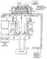
- Fig. 1is a front elevational view, in cross section, of the apparatus of the invention with various elements and their relationship illustrated schematically.
- Fig. 2is a front elevational view in an enlarged scale and broken section of the heating chamber of the apparatus of the invention.
- Fig. 3is a front elevational view, in cross section, illustrating another embodiment of the apparatus of the invention.
- Fig. 4is a heating profile of temperature versus time that depicts typical heating cycle used by the apparatus and process of the invention.
- Fig. 5is another heating profile of temperature versus time that provides a comparison of the heat cycle associated with this invention, and a typical heat cycle associated with a belt furnace performing a similar reflow operation.
- the apparatus 10 for reflowing solder bondshas a container 12 having a stage 14 that supports substrate 16 above the floor 18 of container 12.
- the stage 14can be pegs, fins, or any other suitable structure that engages the bottom surface of substrate 12 and maintains it at a predetermined height in the container.
- Devices 20are shown positioned on and joined to substrate 16 with solder connections 22.
- fluidis pumped into container 12 through opening 24 to contact the bottom surface of substrate 16 to either heat or cool the substrate.
- the level of fluidis controlled by wier 26 as more clearly illustrated in Fig. 2.
- a cover 30can be provided for container 12 to provide an inert gas atmosphere which can also be heated, for heating the devices 20 on substrate 16.
- the cover 30has openings 32 and 34 for introducing and removing inert or heated gas to container 12. Any desirable gas can be introduced and exhausted through openings 32 and 34 including forming gas, hydrogen gas for flux free joining and inert gases.
- the various gasescan be either heated, cooled, or at room temperature.
- a seal 36 positioned between the cover 30 and the top surface of substrate 16confines the chosen environment to the surface area of the substrate and also keeps fluid and fluid vapor from contacting the top surface.
- another seal element 38can be provided between the outer perimeter of cover 30 and container 12.
- the embodiment in Fig. 2also includes an arrangement that provides support for pins 40 during the reflow heating cycle, when the pins are soldered or brazed on the substrate 16.
- the soldermay soften during the heat cycle and stretch the solder securing them to the substrate.
- An apertured platepreferably of graphite, is supported in container 12. Openings 42 have a diameter greater than the diameter of pins 40.
- Openings 42have a diameter greater than the diameter of pins 40.
- the fluidapplies hydraulic pressure against the pins and has a frictional drag on the pins surface which exerts upward forces that aid in supporting the pins.
- Additional openings 44can be provided to permit a greater rate of fluid flow.
- the pattern of the openingscan be varied to achieve uniform heating of the substrate e.g., if corners lag then fewer holes are provided at the center of the substrate and more at the corners.
- any suitable fluidcan be used in the practice of this invention.
- the fluidwill be a liquid, such as oil or the like.
- the fluidmust have a boiling point above the melting point of the solder material being reflowed and a relatively low vapor pressure as well as being non-explosive and non-toxic.
- the fluidshould be sufficiently inert so that the surface of the substrate that it contacts is not degraded nor otherwise adversely affected. I have discovered that a suitable fluid is polyphenyl ether.
- a substrate temperature profile 46consisting of a heat phase 48 where the substrate temperature increases at a rapid rate, a hold phase 50 where the substrate temperature is constant for a short time, and finally a cooling phase 52 where the substrate temperature is decreased rapidly.
- the fluid temperature profile 54is maintained in container 12 by a mechanism to be described. Since there is a time lag between the substrate temperature and the fluid temperature.
- the profile 54 depicting fluid temperaturetherefore is several degrees higher than the substrate temperature as depicted by profile 46. Heating or cooling the substrate with liquid is much faster and more efficient than cooling with air or gas as a heating medium, or radiant heat.
- sump tank 60receiving the fluid from container 12 that has overflowed wier 26 after coming in contact with substrate 16.
- the fluidis cooled and subsequently returned to holding tanks 62 and 64 where the temperature of the fluid is maintained, or the fluid heated.
- the fluidis stored at either a relatively low temperature for cooling purposes or a high temperature for heating purposes.
- Pumps 63 and 65are provided in tanks 62 and 64, respectively, to supply the fluids, properly blended, to achieve the proper temperature to container 12.
- Valves 66 and 68 that control the flow of fluid from pumps 63 and 65shift the flow from circulation within the tank to ensure uniformity of temperature throughout the tank to delivery to the processing containers.
- the computercontrols the speed of the two pumps.
- Computer 70is programmed to provide the proper blend of hot and cool liquids at the proper time to achieve an oil temperature profile, such as depicted in Fig. 4.
- the plumbing and the tanksare enclosed in a chamber 72 and a nitrogen environment maintained therein for safety.
- FIG. 3there is depicted another preferred specific embodiment of the apparatus 80.
- Apparatus 80does not have the capability of providing a closely controlled heating profile possible with apparatus 10.
- the apparatusis useful for removing devices 20 from substrates 16 for rework or for joining devices by manually placing and removing substrates on stage 14.
- the substrate 16is accessible through opening 82 in glove box 84.
- Normally an inert gas environmentis provided in glove box 84.
- Fluidis forced from the sump 60 into chamber 86 by pump 88.
- the fluidis forced upwardly through opening 24 into contact with the substrates 16.
- the fluid after overflowing wier 26flows back to sump 60 and the process is repeated.
- a heating element 90provides control of the fluid temperature.
- Fig. 5 of the drawingillustrates a heating profile 46 of the temperature on the top of ceramic substrate vs. time obtained by using the apparatus and process of this invention using a heated liquid, and subsequently a cooling liquid applied to the bottom surface of the substrate.
- comparison profile 56vs. a plate of temperature on the top of the same ceramic substrate vs. time obtained with a belt furnace.
- the apparatus and method of the inventionis particularly suited for solder bonding integrated circuit semiconductor devices to a ceramic substrate.
- the inventioncan be used for any application where it is advantageous to solder, braze, or otherwise bond elements to a workpiece without exposing the elements and/or the bond to elevated temperatures for lengthy periods of time or otherwise control the temperature for any reason.
- the inventionis useful for bonding I/O pins, capacitors, attachment chips and the like to substrates of any material, and to remove and rebond elements where the assembly must be re-worked to correct for defects and the like.
- the environment on a surface of the substratecan be controlled to protect the elements to be bonded, or achieve conditions that are conducive to bonding integrity.
Landscapes
- Engineering & Computer Science (AREA)
- Computer Hardware Design (AREA)
- Microelectronics & Electronic Packaging (AREA)
- Power Engineering (AREA)
- Manufacturing & Machinery (AREA)
- Mechanical Engineering (AREA)
- Electric Connection Of Electric Components To Printed Circuits (AREA)
- Wire Bonding (AREA)
Description
- The present invention relates generally to solder reflow assembly techniques and apparatus therefor, more particularly to an apparatus and method for forming solder terminals between a substrate and a device, and rework processes.
- A very common technique for joining an electronic element and a supporting substrate is forming solder connections between same. Patents which describes such solder connections and a method of forming these connections are US-A-3.429.040 and 3.495.133. In general solder wettable pads are surrounded by non-solder wettable material, i.e., glass or quartz are provided on the device and also on the substrate. Solder is evaporated through a mask on either the device or substrate and heated to the melting point of the solder which causes it to ball up over the pads into mounds. After the solder balls have solidified, the device is positioned over the substrate with the respective solder pads in alignment, and the assembly heated to again melt or reflow the solder. When the solder balls are remelted and allowed to solidify solder connections are established between the solder wettable pads of the device and substrate. The surface tension of the molten solder will shift the device to correct for minor misalignments. If a device or a connection is defective, the device can be removed and replaced by remelting the solder connections, lifting off the device, and replacing it. When the substrate contains numerous devices, multiple device rework operations may be necessary before all the connections are perfect or to replace devices that fail in use.
- It has been noted that repeated remelting of the solder, and exposure to high temperatures, particularly above 300°C for extended time, as well as a slow rate of cooling from these temperatures causes the formation of intermetallics in solder connections which have a degrading influence. Intermetallics are compounds or alloys of the molecules of the solder and possibly the metals in the pad that have been placed in intimate contact during a process of brazing or soldering. In addition, exposure of the solder terminals to high temperatures causes grain growth within the terminals. Both intermetallics and grain growth degrade the solder connection by making it more brittle and less resistant to stress and strain. Strain is imposed on the solder connections by thermal cycling which normally occurs during use, particularly when the coefficients of expansion of the materials of the device and substrate are different.
- It is conventional to reflow the solder mounds to form a connection by placing the substrate with devices in place on a belt furnace and passing the assembly through the heated environment. The same basic process is used for other solder connections such as I/O pins to a substrate. This exposes the substrate, the device, and the solder bonds to a prolonged heating period, typically on the order of 20 minutes or longer. As the mass of the substrate increased, the non-uniformity of temperature in the substrate increased, the time at elevated temperature increased and the cooling rate decreased. Still further, as the substrate area increases, the number of devices on the substrate increase thereby increasing the probability of more rework operations, each of which requires a device separation and a solder reflow joining operation. Still further, the prolonged heating may damage the devices by degrading the metallurgy and spreading the diffused impurities thus moving the PN junctions and expanding the device impurity regions.
- Other process are disclosed for instance in FR--A-2 206 654 in which the electronic elements are soldered to a substrate by bringing the substrate into contact with a liquid heated to a constant temperature above the solder melting temperature.
- EP-A_5883 discloses an other similar process for soldering components on substrates. Successively, the substrates are preheated, followed by heating to the soldering temperature, after which they are cooled.
- The article entitled "Solder fusing with heated liquids" by D. Schoenthaler and published in "Welding research supplement", Nov. 1974, pages 498S to 509S, shows that the processes of soldering components on a substrate by using heat transfer liquids offer advantages over other heating methods and that the choice of the liquids is important. Glycerol is considered as having excellent fusing characteristics.
- These methods using a heat transfer liquids have the same disadvantages as the processes using a belt furnace, typically, the electronic devices are exposed to a prolonged heating period which may damage them.
- An object of this invention is to provide a new apparatus for reflowing solder connections which materially shortens the time period that the device, the substrate, and the solder connections are exposed to elevated temperatures.
- Another object is to provide more uniform heating of the substrate area.
- Another object of this invention is to provide a new method for reflowing solder connections which materially shortens the time period that the device, the substrate, and the solder connections are exposed to elevated temperatures.
- Yet another object of this invention is to provide an apparatus and a method that will perform solder reflow operations and eliminate or minimize device and solder bond degradation.
- These and other objects of the invention are accomplished by an apparatus for reflowing solder terminals that join an electronic element to a support substrate which includes (1) a stage for supporting the substrate, a quantity of fluid capable of being heated to a temperature in excess of the melting point of the solder of the solder terminals, a means to contact a surface of the substrate with the fluid, the means including at least one reservoir for maintaining fluid at a temperature in excess of the melting point of the solder, and a pumping means to move the fluid from reservoir into contact with a surface of the substrate.
- Other objects, advantages and novel features of the present invention will become apparent from the following detailed description of the invention when considered in conjunction with the accompanying drawings.
- Fig. 1 is a front elevational view, in cross section, of the apparatus of the invention with various elements and their relationship illustrated schematically.
- Fig. 2 is a front elevational view in an enlarged scale and broken section of the heating chamber of the apparatus of the invention.
- Fig. 3 is a front elevational view, in cross section, illustrating another embodiment of the apparatus of the invention.
- Fig. 4 is a heating profile of temperature versus time that depicts typical heating cycle used by the apparatus and process of the invention.
- Fig. 5 is another heating profile of temperature versus time that provides a comparison of the heat cycle associated with this invention, and a typical heat cycle associated with a belt furnace performing a similar reflow operation.
- Referring now to Figs. 1 and 2 there is illustrated a preferred specific embodiment of the invention. The
apparatus 10 for reflowing solder bonds, either to form the solder bonds or to melt bonds that have already been formed so that the substrate and device can be separated, has acontainer 12 having astage 14 that supportssubstrate 16 above thefloor 18 ofcontainer 12. Thestage 14 can be pegs, fins, or any other suitable structure that engages the bottom surface ofsubstrate 12 and maintains it at a predetermined height in the container.Devices 20 are shown positioned on and joined tosubstrate 16 withsolder connections 22. In operation, fluid is pumped intocontainer 12 through opening 24 to contact the bottom surface ofsubstrate 16 to either heat or cool the substrate. The level of fluid is controlled bywier 26 as more clearly illustrated in Fig. 2. The fluid upon overflowing the wire exits the container through opening 28. Acover 30 can be provided forcontainer 12 to provide an inert gas atmosphere which can also be heated, for heating thedevices 20 onsubstrate 16. Thecover 30 hasopenings 32 and 34 for introducing and removing inert or heated gas tocontainer 12. Any desirable gas can be introduced and exhausted throughopenings 32 and 34 including forming gas, hydrogen gas for flux free joining and inert gases. The various gases can be either heated, cooled, or at room temperature. Aseal 36 positioned between thecover 30 and the top surface ofsubstrate 16 confines the chosen environment to the surface area of the substrate and also keeps fluid and fluid vapor from contacting the top surface. As shown in more detail in Fig. 2 anotherseal element 38 can be provided between the outer perimeter ofcover 30 andcontainer 12. The embodiment in Fig. 2 also includes an arrangement that provides support forpins 40 during the reflow heating cycle, when the pins are soldered or brazed on thesubstrate 16. In use the solder may soften during the heat cycle and stretch the solder securing them to the substrate. An apertured plate, preferably of graphite, is supported incontainer 12.Openings 42 have a diameter greater than the diameter ofpins 40. As fluid is pumped intocontainer 12 through opening 24 a portion of the fluid passes between thepins 40 and the walls ofopenings 42. The fluid applies hydraulic pressure against the pins and has a frictional drag on the pins surface which exerts upward forces that aid in supporting the pins.Additional openings 44 can be provided to permit a greater rate of fluid flow. The pattern of the openings can be varied to achieve uniform heating of the substrate e.g., if corners lag then fewer holes are provided at the center of the substrate and more at the corners. - Any suitable fluid can be used in the practice of this invention. Typically the fluid will be a liquid, such as oil or the like. The fluid must have a boiling point above the melting point of the solder material being reflowed and a relatively low vapor pressure as well as being non-explosive and non-toxic. The fluid should be sufficiently inert so that the surface of the substrate that it contacts is not degraded nor otherwise adversely affected. I have discovered that a suitable fluid is polyphenyl ether.
- Referring now to Fig. 4 there is depicted by dashed lines a
substrate temperature profile 46 consisting of aheat phase 48 where the substrate temperature increases at a rapid rate, ahold phase 50 where the substrate temperature is constant for a short time, and finally acooling phase 52 where the substrate temperature is decreased rapidly. In order to achieve this substrate temperature profile, the fluid temperature profile 54 is maintained incontainer 12 by a mechanism to be described. Since there is a time lag between the substrate temperature and the fluid temperature. The profile 54 depicting fluid temperature therefore is several degrees higher than the substrate temperature as depicted byprofile 46. Heating or cooling the substrate with liquid is much faster and more efficient than cooling with air or gas as a heating medium, or radiant heat. Fig. 5 provides a vivid comparison between asubstrate profile 46 using a liquid as a heating and cooling medium, andprofile 56 using heated air or inert gas in a belt furnace, for similar ceramic substrates. Experimental measurements on 90 mm square substrates have shown heat transfer efficiency in oil heating to be 40 times that in the hottest zone of a belt furnace. - Referring now to Fig. 1 of the
drawings sump tank 60 is shown receiving the fluid fromcontainer 12 that has overflowedwier 26 after coming in contact withsubstrate 16. The fluid is cooled and subsequently returned to holdingtanks Pumps 63 and 65 are provided intanks container 12.Valves 66 and 68 that control the flow of fluid frompumps 63 and 65 shift the flow from circulation within the tank to ensure uniformity of temperature throughout the tank to delivery to the processing containers. The computer controls the speed of the two pumps.Computer 70 is programmed to provide the proper blend of hot and cool liquids at the proper time to achieve an oil temperature profile, such as depicted in Fig. 4. Preferably the plumbing and the tanks are enclosed in achamber 72 and a nitrogen environment maintained therein for safety. - In Fig. 3 there is depicted another preferred specific embodiment of the
apparatus 80.Apparatus 80 does not have the capability of providing a closely controlled heating profile possible withapparatus 10. However the apparatus is useful for removingdevices 20 fromsubstrates 16 for rework or for joining devices by manually placing and removing substrates onstage 14. Thesubstrate 16 is accessible throughopening 82 inglove box 84. Normally an inert gas environment is provided inglove box 84. Fluid is forced from thesump 60 into chamber 86 bypump 88. The fluid is forced upwardly throughopening 24 into contact with thesubstrates 16. The fluid after overflowingwier 26 flows back tosump 60 and the process is repeated. Aheating element 90 provides control of the fluid temperature. - Fig. 5 of the drawing illustrates a
heating profile 46 of the temperature on the top of ceramic substrate vs. time obtained by using the apparatus and process of this invention using a heated liquid, and subsequently a cooling liquid applied to the bottom surface of the substrate. By way ofcomparison profile 56 vs. a plate of temperature on the top of the same ceramic substrate vs. time obtained with a belt furnace. These profiles dramatically illustrate the differences in the time a substrate is exposed to elevated temperatures. - The apparatus and method of the invention is particularly suited for solder bonding integrated circuit semiconductor devices to a ceramic substrate. However, the invention can be used for any application where it is advantageous to solder, braze, or otherwise bond elements to a workpiece without exposing the elements and/or the bond to elevated temperatures for lengthy periods of time or otherwise control the temperature for any reason. In particular, the invention is useful for bonding I/O pins, capacitors, attachment chips and the like to substrates of any material, and to remove and rebond elements where the assembly must be re-worked to correct for defects and the like. In the preferred embodiment, the environment on a surface of the substrate can be controlled to protect the elements to be bonded, or achieve conditions that are conducive to bonding integrity.
Claims (15)
- An apparatus (10) for reflowing solder terminals (22) that join an electronic element (20) to a support substrate (16) comprising:
a stage (14) for supporting said substrate,
a quantity of fluid capable of being heated to a temperature in excess of the melting point of the solder of said solder terminals,
a means to supply fluid to contact a surface of said substrate (16) with said fluid, said means being connected to at least one reservoir (62, 64), and
a pumping means (63, 65) to move said liquid from said reservoir into contact with a surface,
this apparatus being characterized in that it further comprises:
a means (66, 68, 70) to control the temperature of said fluid being supplied to contact said substrate to initially increase the temperature of the fluid, and subsequently to reduce the temperature of said fluid, wherein the temperature of said fluid in contact with said substrate is varied according to said control means. - The apparatus of Claim 1 where said electronic element (20) is mounted on the top surface of said substrate (16), and said means to contact the substrate with fluid contacts the bottom surface of said substrate with heated fluid.
- The apparatus of Claim 2 wherein said means to supply fluid to contact the substrate is connected to at least two fluid reservoirs (62, 64) that hold fluid at different temperatures, a fluid pump (63, 65) and a mixing valve (66, 68) being associated with each fluid reservoir, said control means controlling said fluid pumps and said mixing valves (66, 68) to supply heated fluid at varying temperatures to contact said substrate.
- The apparatus of Claim 3 wherein said electronic device is an integrated semiconductor device having a plurality of solder terminals to be joined to corresponding solder pads on the top surface of said substrate, and said substrate is a multilayer ceramic substrate provided with I/O pins on the bottom surface.
- The apparatus of Claim 4 wherein said means to contact the substrate with fluid further includes a container (12) to receive and support said substrate therein at a predetermined height, and a wier (26) to maintain the level of fluid in the container at a height to maintain contact of fluid with the bottom surface of said substrate.
- The apparatus of Claim 5 which further includes a plate provided with apertures (42) for receiving said I/O pins (40), said apertures of a size to provide clearance about said pins to allow fluid flow between the aperture wall and pin, and said container includes a cover element (30), a seal element (38) positioned between said cover element and a substrate supported in said container to thereby form a sealed enclosure over the top surface of said device mounted on the top surface.
- The apparatus of Claim 6 wherein a means (32, 34) is provided to introduce and circulate an inert or reducing gas into and through said sealed enclosure.
- The apparatus of Claim 3 wherein a first fluid reservoir (64) contains heated fluid, and a second fluid reservoir (62) contains cool fluid, said control means acting to mix fluids from said first reservoir and said second reservoir to increase the temperature of said fluid contacting said substrate to above the melting point of said solder, and subsequently reduce the temperature of fluid contacting said substrate, and a sump tank (60) for accepting the fluid after it has contacted said substrate, and a conduit means is provided to return fluid from said sump tank to said fluid reservoir and said second fluid reservoir.
- The apparatus of Claim 8 wherein a heating means is provided in each of said first and said second fluid reservoirs, and said fluid is polyphenyl ether.
- The apparatus of Claim 1 wherein said reservoir has an opening on the top thereof (Fig. 3), and which further includes:
a support for holding said substrate over said opening,
a wier (26) surrounding said opening for maintaining a fluid level above the bottom surface of a substrate when positioned on said support,
and a sump for collecting fluid overflowing said wier,
a glove box (84) over said substrate,
and wherein:
said pump means moves fluid from said sump into said fluid reservoir,
said fluid is polyphenyl ether,
a means is provided to maintain an insert gas environment in said glove box,
a means is provided to heat said gas introduced to said sealed enclosure. - The apparatus of Claim 6 wherein additional apertures are provided in said plate to direct additional fluid against said substrate to assist in achieving a more uniform top surface temperature on said substrate.
- A method of reflowing solder terminals that join an electronic device to a substrate, comprising the steps of:
contacting the bottom surface of said substrate with a circulating liquid,
controlling the temperature of said liquid being supplied to contact said substrate so that the temperature of said liquid in contact with said substrate is varied, comprising:
increasing the temperature of said liquid from a temperature below the melting point of the solder to a temperature exceeding the melting point of the solder material of said solder terminals, and
subsequently decreasing the temperature of said liquid to a temperature below melting point of said solder material,
said liquid flowing towards said substrate from a first and a second tanks where the temperature is maintained above and under the solder melting temperature respectively. - The method of claim 12 wherein said electronic device is an integrated semiconductor device provided with a plurality of solder pads distributed over the bottom side, and said substrate is a multilayer ceramic substrate with a corresponding plurality of solder pads on the top surface.
- The method of claim 13 wherein the entire heating and cooling cycle is less than five minutes in duration.
- The method of Claim 12 wherein the solder material of said terminals is reflowed to establish electrical connections.
Applications Claiming Priority (2)
| Application Number | Priority Date | Filing Date | Title |
|---|---|---|---|
| US856516 | 1986-04-28 | ||
| US06/856,516US4747533A (en) | 1986-04-28 | 1986-04-28 | Bonding method and apparatus |
Publications (3)
| Publication Number | Publication Date |
|---|---|
| EP0243621A2 EP0243621A2 (en) | 1987-11-04 |
| EP0243621A3 EP0243621A3 (en) | 1990-05-16 |
| EP0243621B1true EP0243621B1 (en) | 1993-12-29 |
Family
ID=25323824
Family Applications (1)
| Application Number | Title | Priority Date | Filing Date |
|---|---|---|---|
| EP87103203AExpired - LifetimeEP0243621B1 (en) | 1986-04-28 | 1987-03-06 | Bonding method and apparatus |
Country Status (4)
| Country | Link |
|---|---|
| US (1) | US4747533A (en) |
| EP (1) | EP0243621B1 (en) |
| JP (1) | JPS62257737A (en) |
| DE (1) | DE3788589T2 (en) |
Families Citing this family (9)
| Publication number | Priority date | Publication date | Assignee | Title |
|---|---|---|---|---|
| US5102028A (en)* | 1990-04-02 | 1992-04-07 | International Business Machines Corporation | Localized soldering station using state changing medium |
| DE4024181C1 (en)* | 1990-07-30 | 1992-02-13 | Siemens Nixdorf Informationssysteme Ag, 4790 Paderborn, De | Vapour phase soldering installation - has valve in by=pass opening in dependence on preset temp. of sec. medium in soldering tank |
| JP4271299B2 (en)* | 1999-06-28 | 2009-06-03 | 光洋サーモシステム株式会社 | Reflow furnace |
| EP1270130B1 (en)* | 2001-06-20 | 2010-03-24 | ALSTOM Technology Ltd | Soldered joint and method for producing a soldered joint |
| JP2007180447A (en)* | 2005-12-28 | 2007-07-12 | Toyota Industries Corp | Soldering method, soldering apparatus, and method of manufacturing semiconductor device |
| JP4640170B2 (en)* | 2005-12-28 | 2011-03-02 | 株式会社豊田自動織機 | Soldering method, semiconductor module manufacturing method, and soldering apparatus |
| JP4375491B1 (en)* | 2008-06-23 | 2009-12-02 | 日本ジョイント株式会社 | Electronic component soldering apparatus and soldering method |
| US9166139B2 (en)* | 2009-05-14 | 2015-10-20 | The Neothermal Energy Company | Method for thermally cycling an object including a polarizable material |
| US11445650B2 (en)* | 2019-10-22 | 2022-09-13 | International Business Machines Corporation | Localized rework using liquid media soldering |
Family Cites Families (19)
| Publication number | Priority date | Publication date | Assignee | Title |
|---|---|---|---|---|
| US30399A (en)* | 1860-10-16 | Gas-kegttlatob | ||
| US3054174A (en)* | 1958-05-13 | 1962-09-18 | Rca Corp | Method for making semiconductor devices |
| US3825994A (en)* | 1972-11-15 | 1974-07-30 | Rca Corp | Method of soldering circuit components to a substrate |
| US4077467A (en)* | 1976-01-28 | 1978-03-07 | Spigarelli Donald J | Method and apparatus for soldering, fusing or brazing |
| US4055217A (en)* | 1976-02-02 | 1977-10-25 | Western Electric Company, Inc. | Method for maintaining a vapor blanket in a condensation heating facility |
| USRE30399E (en) | 1977-08-19 | 1980-09-09 | Western Electric Co., Inc. | Method for soldering, fusing or brazing |
| NL7805800A (en)* | 1978-05-29 | 1979-12-03 | Philips Nv | METHOD AND DEVICE FOR SOLDERING COMPONENTS ON A HOLLESS THICK-FILM SUBSTRATE AND THICK-FILM SUBSTRATE WITH PARTS SOLDERED BY THE PROCESS. |
| US4334646A (en)* | 1980-04-17 | 1982-06-15 | Harris Corporation | Method of solder reflow assembly |
| DE3040274C2 (en)* | 1980-10-23 | 1983-06-09 | ERSA Ernst Sachs KG, GmbH & Co, 6980 Wertheim | Device for unsoldering electronic components from printed circuit boards |
| JPS57141993A (en)* | 1981-02-25 | 1982-09-02 | Matsushita Electric Industrial Co Ltd | Printed circuit board mounted with chip part and method of mounting chip part on printed circuit board |
| US4441647A (en)* | 1982-06-04 | 1984-04-10 | Northern Telecom Limited | Resoldering tool for ceramic substrate hybrid electronic circuits |
| US4474322A (en)* | 1982-11-12 | 1984-10-02 | Epe Corporation | Displacement soldering device |
| GB8312503D0 (en)* | 1983-05-06 | 1983-06-08 | Isc Chemicals Ltd | Vapour phase soldering |
| US4538757A (en)* | 1983-08-01 | 1985-09-03 | Motorola, Inc. | Wave soldering in a reducing atmosphere |
| FR2556083B1 (en)* | 1983-10-11 | 1986-04-25 | Piezo Ceram Electronique | IMPROVED MACHINE FOR HEATING AN ARTICLE OR PRODUCT BY CONDENSATION OF STEAM THEREON |
| US4561584A (en)* | 1983-10-17 | 1985-12-31 | Storage Technology Partners | Integrated circuit package removal |
| US4561586A (en)* | 1984-09-04 | 1985-12-31 | Burroughs Corporation | Method of removing a soldered integrated circuit package from a printed circuit board |
| US4580716A (en)* | 1984-10-17 | 1986-04-08 | Rca Corporation | Apparatus and method for vapor phase solder reflow |
| JPS6264475A (en)* | 1985-09-17 | 1987-03-23 | Kenji Kondo | Fusion joining device for article |
- 1986
- 1986-04-28USUS06/856,516patent/US4747533A/ennot_activeExpired - Fee Related
- 1987
- 1987-03-03JPJP62046944Apatent/JPS62257737A/enactiveGranted
- 1987-03-06DEDE3788589Tpatent/DE3788589T2/ennot_activeExpired - Fee Related
- 1987-03-06EPEP87103203Apatent/EP0243621B1/ennot_activeExpired - Lifetime
Also Published As
| Publication number | Publication date |
|---|---|
| US4747533A (en) | 1988-05-31 |
| DE3788589D1 (en) | 1994-02-10 |
| EP0243621A3 (en) | 1990-05-16 |
| JPH0432542B2 (en) | 1992-05-29 |
| DE3788589T2 (en) | 1994-06-30 |
| EP0243621A2 (en) | 1987-11-04 |
| JPS62257737A (en) | 1987-11-10 |
Similar Documents
| Publication | Publication Date | Title |
|---|---|---|
| EP0918354B1 (en) | Method for wafer-scale assembly of chip-size packages | |
| US5816473A (en) | Method of fabricating electronic circuit device and apparatus for performing the same method | |
| JP4759509B2 (en) | Solder bump forming method and apparatus | |
| EP0243621B1 (en) | Bonding method and apparatus | |
| KR100669061B1 (en) | Reflow Soldering Method | |
| US8925170B2 (en) | Method for removing an electronic component from a substrate | |
| JPH10308465A (en) | Cast metal seal for semiconductor substrate | |
| US6705506B1 (en) | Inert atmosphere soldering apparatus | |
| US20060065431A1 (en) | Self-reflowing printed circuit board and application methods | |
| EP0145975B1 (en) | Apparatus and method for heating objects eg chips during soldering, to and maintaining them at a desired temperature | |
| US6808958B2 (en) | Methods of bonding microelectronic elements | |
| JP3718671B2 (en) | System and method for mounting electronic components on a flexible substrate | |
| RU2329624C2 (en) | Method and device for soldering by reflowed solder with control of volume flow | |
| JPS6157720B2 (en) | ||
| US5860582A (en) | Inert atmosphere soldering apparatus | |
| US4805831A (en) | Bonding method | |
| US4802276A (en) | Apparatus for printed wiring board component assembly | |
| CN100521131C (en) | Heating device and reflow soldering device | |
| JP2002373923A (en) | Method and apparatus for removing interconnections | |
| US20010052536A1 (en) | Method and apparatus for making an electrical device | |
| JP3753524B2 (en) | Manufacturing method of electronic parts | |
| Pandey et al. | Thermal profile optimization for ceramic column grid array package assembly in selective reflow system for high reliability applications | |
| Puttlitz et al. | Solder transfer technique for flip-chip and electronic assembly applications | |
| JPH01289566A (en) | Vapor phase/reflow soldering device | |
| US5845838A (en) | Process for remelting a contact surface metallization |
Legal Events
| Date | Code | Title | Description |
|---|---|---|---|
| PUAI | Public reference made under article 153(3) epc to a published international application that has entered the european phase | Free format text:ORIGINAL CODE: 0009012 | |
| AK | Designated contracting states | Kind code of ref document:A2 Designated state(s):DE FR GB IT | |
| 17P | Request for examination filed | Effective date:19880224 | |
| PUAL | Search report despatched | Free format text:ORIGINAL CODE: 0009013 | |
| AK | Designated contracting states | Kind code of ref document:A3 Designated state(s):DE FR GB IT | |
| 17Q | First examination report despatched | Effective date:19910704 | |
| GRAA | (expected) grant | Free format text:ORIGINAL CODE: 0009210 | |
| AK | Designated contracting states | Kind code of ref document:B1 Designated state(s):DE FR GB IT | |
| PG25 | Lapsed in a contracting state [announced via postgrant information from national office to epo] | Ref country code:IT Free format text:LAPSE BECAUSE OF FAILURE TO SUBMIT A TRANSLATION OF THE DESCRIPTION OR TO PAY THE FEE WITHIN THE PRESCRIBED TIME-LIMIT;WARNING: LAPSES OF ITALIAN PATENTS WITH EFFECTIVE DATE BEFORE 2007 MAY HAVE OCCURRED AT ANY TIME BEFORE 2007. THE CORRECT EFFECTIVE DATE MAY BE DIFFERENT FROM THE ONE RECORDED. Effective date:19931229 | |
| REF | Corresponds to: | Ref document number:3788589 Country of ref document:DE Date of ref document:19940210 | |
| ET | Fr: translation filed | ||
| PLBE | No opposition filed within time limit | Free format text:ORIGINAL CODE: 0009261 | |
| STAA | Information on the status of an ep patent application or granted ep patent | Free format text:STATUS: NO OPPOSITION FILED WITHIN TIME LIMIT | |
| 26N | No opposition filed | ||
| PGFP | Annual fee paid to national office [announced via postgrant information from national office to epo] | Ref country code:DE Payment date:19950330 Year of fee payment:9 | |
| PGFP | Annual fee paid to national office [announced via postgrant information from national office to epo] | Ref country code:FR Payment date:19960307 Year of fee payment:10 | |
| PG25 | Lapsed in a contracting state [announced via postgrant information from national office to epo] | Ref country code:DE Effective date:19961203 | |
| PGFP | Annual fee paid to national office [announced via postgrant information from national office to epo] | Ref country code:GB Payment date:19970224 Year of fee payment:11 | |
| PG25 | Lapsed in a contracting state [announced via postgrant information from national office to epo] | Ref country code:FR Free format text:LAPSE BECAUSE OF NON-PAYMENT OF DUE FEES Effective date:19971128 | |
| REG | Reference to a national code | Ref country code:FR Ref legal event code:ST | |
| PG25 | Lapsed in a contracting state [announced via postgrant information from national office to epo] | Ref country code:GB Free format text:LAPSE BECAUSE OF NON-PAYMENT OF DUE FEES Effective date:19980306 | |
| GBPC | Gb: european patent ceased through non-payment of renewal fee | Effective date:19980306 |