EP0236404B1 - Manufacture of electrical circuits - Google Patents
Manufacture of electrical circuitsDownload PDFInfo
- Publication number
- EP0236404B1 EP0236404B1EP86905344AEP86905344AEP0236404B1EP 0236404 B1EP0236404 B1EP 0236404B1EP 86905344 AEP86905344 AEP 86905344AEP 86905344 AEP86905344 AEP 86905344AEP 0236404 B1EP0236404 B1EP 0236404B1
- Authority
- EP
- European Patent Office
- Prior art keywords
- carrier
- substrate
- circuit
- face
- embedded
- Prior art date
- Legal status (The legal status is an assumption and is not a legal conclusion. Google has not performed a legal analysis and makes no representation as to the accuracy of the status listed.)
- Expired - Lifetime
Links
- 238000004519manufacturing processMethods0.000titledescription2
- 239000000758substrateSubstances0.000claimsabstractdescription47
- 239000000463materialSubstances0.000claimsabstractdescription25
- 238000000034methodMethods0.000claimsabstractdescription21
- 239000004033plasticSubstances0.000claimsabstractdescription7
- 229920003023plasticPolymers0.000claimsabstractdescription7
- 229920001169thermoplasticPolymers0.000claimsdescription8
- 239000004416thermosoftening plasticSubstances0.000claimsdescription8
- 239000012876carrier materialSubstances0.000claimsdescription6
- 239000003822epoxy resinSubstances0.000claimsdescription4
- 229920000647polyepoxidePolymers0.000claimsdescription4
- 239000004697PolyetherimideSubstances0.000claimsdescription3
- 229920001601polyetherimidePolymers0.000claimsdescription3
- 238000007639printingMethods0.000claimsdescription2
- 239000000155meltSubstances0.000claims2
- 230000000295complement effectEffects0.000claims1
- 229920006015heat resistant resinPolymers0.000claims1
- 229920006230thermoplastic polyester resinPolymers0.000claims1
- 238000000465mouldingMethods0.000abstractdescription20
- 239000000976inkSubstances0.000description8
- 229920004738ULTEM®Polymers0.000description5
- 239000004020conductorSubstances0.000description4
- 238000000151depositionMethods0.000description3
- 238000002347injectionMethods0.000description3
- 239000007924injectionSubstances0.000description3
- 238000001746injection mouldingMethods0.000description3
- 239000010410layerSubstances0.000description3
- 238000010276constructionMethods0.000description2
- 229920005989resinPolymers0.000description2
- 239000011347resinSubstances0.000description2
- 238000003856thermoformingMethods0.000description2
- 239000012815thermoplastic materialSubstances0.000description2
- RYGMFSIKBFXOCR-UHFFFAOYSA-NCopperChemical compound[Cu]RYGMFSIKBFXOCR-UHFFFAOYSA-N0.000description1
- 239000004642PolyimideSubstances0.000description1
- BQCADISMDOOEFD-UHFFFAOYSA-NSilverChemical compound[Ag]BQCADISMDOOEFD-UHFFFAOYSA-N0.000description1
- 239000000654additiveSubstances0.000description1
- 230000000996additive effectEffects0.000description1
- 239000002313adhesive filmSubstances0.000description1
- 238000000429assemblyMethods0.000description1
- 239000003990capacitorSubstances0.000description1
- 238000011109contaminationMethods0.000description1
- 238000010924continuous productionMethods0.000description1
- 229910052802copperInorganic materials0.000description1
- 239000010949copperSubstances0.000description1
- 239000000428dustSubstances0.000description1
- 229920006351engineering plasticPolymers0.000description1
- 230000004907fluxEffects0.000description1
- 239000011888foilSubstances0.000description1
- 238000003780insertionMethods0.000description1
- 230000037431insertionEffects0.000description1
- 239000011810insulating materialSubstances0.000description1
- 238000009413insulationMethods0.000description1
- 239000011229interlayerSubstances0.000description1
- UQSXHKLRYXJYBZ-UHFFFAOYSA-Niron oxideInorganic materials[Fe]=OUQSXHKLRYXJYBZ-UHFFFAOYSA-N0.000description1
- 229910000510noble metalInorganic materials0.000description1
- NDLPOXTZKUMGOV-UHFFFAOYSA-Noxo(oxoferriooxy)iron hydrateChemical compoundO.O=[Fe]O[Fe]=ONDLPOXTZKUMGOV-UHFFFAOYSA-N0.000description1
- WXZMFSXDPGVJKK-UHFFFAOYSA-NpentaerythritolChemical classOCC(CO)(CO)COWXZMFSXDPGVJKK-UHFFFAOYSA-N0.000description1
- 229920003223poly(pyromellitimide-1,4-diphenyl ether)Polymers0.000description1
- 229920001225polyester resinPolymers0.000description1
- 239000004645polyester resinSubstances0.000description1
- 229920001721polyimidePolymers0.000description1
- 238000007493shaping processMethods0.000description1
- 229910000679solderInorganic materials0.000description1
- 229910001220stainless steelInorganic materials0.000description1
- 239000010935stainless steelSubstances0.000description1
- 229920001187thermosetting polymerPolymers0.000description1
- 239000004634thermosetting polymerSubstances0.000description1
Images


Classifications
- H—ELECTRICITY
- H05—ELECTRIC TECHNIQUES NOT OTHERWISE PROVIDED FOR
- H05K—PRINTED CIRCUITS; CASINGS OR CONSTRUCTIONAL DETAILS OF ELECTRIC APPARATUS; MANUFACTURE OF ASSEMBLAGES OF ELECTRICAL COMPONENTS
- H05K1/00—Printed circuits
- B—PERFORMING OPERATIONS; TRANSPORTING
- B29—WORKING OF PLASTICS; WORKING OF SUBSTANCES IN A PLASTIC STATE IN GENERAL
- B29C—SHAPING OR JOINING OF PLASTICS; SHAPING OF MATERIAL IN A PLASTIC STATE, NOT OTHERWISE PROVIDED FOR; AFTER-TREATMENT OF THE SHAPED PRODUCTS, e.g. REPAIRING
- B29C45/00—Injection moulding, i.e. forcing the required volume of moulding material through a nozzle into a closed mould; Apparatus therefor
- B29C45/0053—Injection moulding, i.e. forcing the required volume of moulding material through a nozzle into a closed mould; Apparatus therefor combined with a final operation, e.g. shaping
- B29C45/0055—Shaping
- B—PERFORMING OPERATIONS; TRANSPORTING
- B29—WORKING OF PLASTICS; WORKING OF SUBSTANCES IN A PLASTIC STATE IN GENERAL
- B29C—SHAPING OR JOINING OF PLASTICS; SHAPING OF MATERIAL IN A PLASTIC STATE, NOT OTHERWISE PROVIDED FOR; AFTER-TREATMENT OF THE SHAPED PRODUCTS, e.g. REPAIRING
- B29C45/00—Injection moulding, i.e. forcing the required volume of moulding material through a nozzle into a closed mould; Apparatus therefor
- B29C45/14—Injection moulding, i.e. forcing the required volume of moulding material through a nozzle into a closed mould; Apparatus therefor incorporating preformed parts or layers, e.g. injection moulding around inserts or for coating articles
- B29C45/1418—Injection moulding, i.e. forcing the required volume of moulding material through a nozzle into a closed mould; Apparatus therefor incorporating preformed parts or layers, e.g. injection moulding around inserts or for coating articles the inserts being deformed or preformed, e.g. by the injection pressure
- B—PERFORMING OPERATIONS; TRANSPORTING
- B29—WORKING OF PLASTICS; WORKING OF SUBSTANCES IN A PLASTIC STATE IN GENERAL
- B29C—SHAPING OR JOINING OF PLASTICS; SHAPING OF MATERIAL IN A PLASTIC STATE, NOT OTHERWISE PROVIDED FOR; AFTER-TREATMENT OF THE SHAPED PRODUCTS, e.g. REPAIRING
- B29C70/00—Shaping composites, i.e. plastics material comprising reinforcements, fillers or preformed parts, e.g. inserts
- B29C70/68—Shaping composites, i.e. plastics material comprising reinforcements, fillers or preformed parts, e.g. inserts by incorporating or moulding on preformed parts, e.g. inserts or layers, e.g. foam blocks
- B29C70/78—Moulding material on one side only of the preformed part
- H—ELECTRICITY
- H05—ELECTRIC TECHNIQUES NOT OTHERWISE PROVIDED FOR
- H05K—PRINTED CIRCUITS; CASINGS OR CONSTRUCTIONAL DETAILS OF ELECTRIC APPARATUS; MANUFACTURE OF ASSEMBLAGES OF ELECTRICAL COMPONENTS
- H05K3/00—Apparatus or processes for manufacturing printed circuits
- H05K3/0011—Working of insulating substrates or insulating layers
- H05K3/0014—Shaping of the substrate, e.g. by moulding
- H—ELECTRICITY
- H05—ELECTRIC TECHNIQUES NOT OTHERWISE PROVIDED FOR
- H05K—PRINTED CIRCUITS; CASINGS OR CONSTRUCTIONAL DETAILS OF ELECTRIC APPARATUS; MANUFACTURE OF ASSEMBLAGES OF ELECTRICAL COMPONENTS
- H05K3/00—Apparatus or processes for manufacturing printed circuits
- H05K3/10—Apparatus or processes for manufacturing printed circuits in which conductive material is applied to the insulating support in such a manner as to form the desired conductive pattern
- H05K3/20—Apparatus or processes for manufacturing printed circuits in which conductive material is applied to the insulating support in such a manner as to form the desired conductive pattern by affixing prefabricated conductor pattern
- H05K3/207—Apparatus or processes for manufacturing printed circuits in which conductive material is applied to the insulating support in such a manner as to form the desired conductive pattern by affixing prefabricated conductor pattern using a prefabricated paste pattern, ink pattern or powder pattern
- B—PERFORMING OPERATIONS; TRANSPORTING
- B29—WORKING OF PLASTICS; WORKING OF SUBSTANCES IN A PLASTIC STATE IN GENERAL
- B29C—SHAPING OR JOINING OF PLASTICS; SHAPING OF MATERIAL IN A PLASTIC STATE, NOT OTHERWISE PROVIDED FOR; AFTER-TREATMENT OF THE SHAPED PRODUCTS, e.g. REPAIRING
- B29C45/00—Injection moulding, i.e. forcing the required volume of moulding material through a nozzle into a closed mould; Apparatus therefor
- B29C45/14—Injection moulding, i.e. forcing the required volume of moulding material through a nozzle into a closed mould; Apparatus therefor incorporating preformed parts or layers, e.g. injection moulding around inserts or for coating articles
- B29C45/1418—Injection moulding, i.e. forcing the required volume of moulding material through a nozzle into a closed mould; Apparatus therefor incorporating preformed parts or layers, e.g. injection moulding around inserts or for coating articles the inserts being deformed or preformed, e.g. by the injection pressure
- B29C2045/14237—Injection moulding, i.e. forcing the required volume of moulding material through a nozzle into a closed mould; Apparatus therefor incorporating preformed parts or layers, e.g. injection moulding around inserts or for coating articles the inserts being deformed or preformed, e.g. by the injection pressure the inserts being deformed or preformed outside the mould or mould cavity
- B—PERFORMING OPERATIONS; TRANSPORTING
- B29—WORKING OF PLASTICS; WORKING OF SUBSTANCES IN A PLASTIC STATE IN GENERAL
- B29C—SHAPING OR JOINING OF PLASTICS; SHAPING OF MATERIAL IN A PLASTIC STATE, NOT OTHERWISE PROVIDED FOR; AFTER-TREATMENT OF THE SHAPED PRODUCTS, e.g. REPAIRING
- B29C2791/00—Shaping characteristics in general
- B29C2791/004—Shaping under special conditions
- B29C2791/006—Using vacuum
- B—PERFORMING OPERATIONS; TRANSPORTING
- B29—WORKING OF PLASTICS; WORKING OF SUBSTANCES IN A PLASTIC STATE IN GENERAL
- B29C—SHAPING OR JOINING OF PLASTICS; SHAPING OF MATERIAL IN A PLASTIC STATE, NOT OTHERWISE PROVIDED FOR; AFTER-TREATMENT OF THE SHAPED PRODUCTS, e.g. REPAIRING
- B29C45/00—Injection moulding, i.e. forcing the required volume of moulding material through a nozzle into a closed mould; Apparatus therefor
- B29C45/14—Injection moulding, i.e. forcing the required volume of moulding material through a nozzle into a closed mould; Apparatus therefor incorporating preformed parts or layers, e.g. injection moulding around inserts or for coating articles
- B29C45/14639—Injection moulding, i.e. forcing the required volume of moulding material through a nozzle into a closed mould; Apparatus therefor incorporating preformed parts or layers, e.g. injection moulding around inserts or for coating articles for obtaining an insulating effect, e.g. for electrical components
- B—PERFORMING OPERATIONS; TRANSPORTING
- B29—WORKING OF PLASTICS; WORKING OF SUBSTANCES IN A PLASTIC STATE IN GENERAL
- B29C—SHAPING OR JOINING OF PLASTICS; SHAPING OF MATERIAL IN A PLASTIC STATE, NOT OTHERWISE PROVIDED FOR; AFTER-TREATMENT OF THE SHAPED PRODUCTS, e.g. REPAIRING
- B29C45/00—Injection moulding, i.e. forcing the required volume of moulding material through a nozzle into a closed mould; Apparatus therefor
- B29C45/14—Injection moulding, i.e. forcing the required volume of moulding material through a nozzle into a closed mould; Apparatus therefor incorporating preformed parts or layers, e.g. injection moulding around inserts or for coating articles
- B29C45/14778—Injection moulding, i.e. forcing the required volume of moulding material through a nozzle into a closed mould; Apparatus therefor incorporating preformed parts or layers, e.g. injection moulding around inserts or for coating articles the article consisting of a material with particular properties, e.g. porous, brittle
- B—PERFORMING OPERATIONS; TRANSPORTING
- B29—WORKING OF PLASTICS; WORKING OF SUBSTANCES IN A PLASTIC STATE IN GENERAL
- B29C—SHAPING OR JOINING OF PLASTICS; SHAPING OF MATERIAL IN A PLASTIC STATE, NOT OTHERWISE PROVIDED FOR; AFTER-TREATMENT OF THE SHAPED PRODUCTS, e.g. REPAIRING
- B29C45/00—Injection moulding, i.e. forcing the required volume of moulding material through a nozzle into a closed mould; Apparatus therefor
- B29C45/14—Injection moulding, i.e. forcing the required volume of moulding material through a nozzle into a closed mould; Apparatus therefor incorporating preformed parts or layers, e.g. injection moulding around inserts or for coating articles
- B29C45/14827—Injection moulding, i.e. forcing the required volume of moulding material through a nozzle into a closed mould; Apparatus therefor incorporating preformed parts or layers, e.g. injection moulding around inserts or for coating articles using a transfer foil detachable from the insert
- B—PERFORMING OPERATIONS; TRANSPORTING
- B29—WORKING OF PLASTICS; WORKING OF SUBSTANCES IN A PLASTIC STATE IN GENERAL
- B29C—SHAPING OR JOINING OF PLASTICS; SHAPING OF MATERIAL IN A PLASTIC STATE, NOT OTHERWISE PROVIDED FOR; AFTER-TREATMENT OF THE SHAPED PRODUCTS, e.g. REPAIRING
- B29C51/00—Shaping by thermoforming, i.e. shaping sheets or sheet like preforms after heating, e.g. shaping sheets in matched moulds or by deep-drawing; Apparatus therefor
- B29C51/08—Deep drawing or matched-mould forming, i.e. using mechanical means only
- B29C51/082—Deep drawing or matched-mould forming, i.e. using mechanical means only by shaping between complementary mould parts
- B—PERFORMING OPERATIONS; TRANSPORTING
- B29—WORKING OF PLASTICS; WORKING OF SUBSTANCES IN A PLASTIC STATE IN GENERAL
- B29C—SHAPING OR JOINING OF PLASTICS; SHAPING OF MATERIAL IN A PLASTIC STATE, NOT OTHERWISE PROVIDED FOR; AFTER-TREATMENT OF THE SHAPED PRODUCTS, e.g. REPAIRING
- B29C51/00—Shaping by thermoforming, i.e. shaping sheets or sheet like preforms after heating, e.g. shaping sheets in matched moulds or by deep-drawing; Apparatus therefor
- B29C51/10—Forming by pressure difference, e.g. vacuum
- B—PERFORMING OPERATIONS; TRANSPORTING
- B29—WORKING OF PLASTICS; WORKING OF SUBSTANCES IN A PLASTIC STATE IN GENERAL
- B29C—SHAPING OR JOINING OF PLASTICS; SHAPING OF MATERIAL IN A PLASTIC STATE, NOT OTHERWISE PROVIDED FOR; AFTER-TREATMENT OF THE SHAPED PRODUCTS, e.g. REPAIRING
- B29C51/00—Shaping by thermoforming, i.e. shaping sheets or sheet like preforms after heating, e.g. shaping sheets in matched moulds or by deep-drawing; Apparatus therefor
- B29C51/14—Shaping by thermoforming, i.e. shaping sheets or sheet like preforms after heating, e.g. shaping sheets in matched moulds or by deep-drawing; Apparatus therefor using multilayered preforms or sheets
- B—PERFORMING OPERATIONS; TRANSPORTING
- B29—WORKING OF PLASTICS; WORKING OF SUBSTANCES IN A PLASTIC STATE IN GENERAL
- B29K—INDEXING SCHEME ASSOCIATED WITH SUBCLASSES B29B, B29C OR B29D, RELATING TO MOULDING MATERIALS OR TO MATERIALS FOR MOULDS, REINFORCEMENTS, FILLERS OR PREFORMED PARTS, e.g. INSERTS
- B29K2067/00—Use of polyesters or derivatives thereof, as moulding material
- B—PERFORMING OPERATIONS; TRANSPORTING
- B29—WORKING OF PLASTICS; WORKING OF SUBSTANCES IN A PLASTIC STATE IN GENERAL
- B29K—INDEXING SCHEME ASSOCIATED WITH SUBCLASSES B29B, B29C OR B29D, RELATING TO MOULDING MATERIALS OR TO MATERIALS FOR MOULDS, REINFORCEMENTS, FILLERS OR PREFORMED PARTS, e.g. INSERTS
- B29K2995/00—Properties of moulding materials, reinforcements, fillers, preformed parts or moulds
- B29K2995/0003—Properties of moulding materials, reinforcements, fillers, preformed parts or moulds having particular electrical or magnetic properties, e.g. piezoelectric
- B29K2995/0005—Conductive
- B—PERFORMING OPERATIONS; TRANSPORTING
- B29—WORKING OF PLASTICS; WORKING OF SUBSTANCES IN A PLASTIC STATE IN GENERAL
- B29L—INDEXING SCHEME ASSOCIATED WITH SUBCLASS B29C, RELATING TO PARTICULAR ARTICLES
- B29L2009/00—Layered products
- B29L2009/005—Layered products coated
- B29L2009/008—Layered products coated metalized, galvanized
- B—PERFORMING OPERATIONS; TRANSPORTING
- B29—WORKING OF PLASTICS; WORKING OF SUBSTANCES IN A PLASTIC STATE IN GENERAL
- B29L—INDEXING SCHEME ASSOCIATED WITH SUBCLASS B29C, RELATING TO PARTICULAR ARTICLES
- B29L2031/00—Other particular articles
- B29L2031/34—Electrical apparatus, e.g. sparking plugs or parts thereof
- B29L2031/3425—Printed circuits
- H—ELECTRICITY
- H05—ELECTRIC TECHNIQUES NOT OTHERWISE PROVIDED FOR
- H05K—PRINTED CIRCUITS; CASINGS OR CONSTRUCTIONAL DETAILS OF ELECTRIC APPARATUS; MANUFACTURE OF ASSEMBLAGES OF ELECTRICAL COMPONENTS
- H05K1/00—Printed circuits
- H05K1/02—Details
- H05K1/0284—Details of three-dimensional rigid printed circuit boards
- H—ELECTRICITY
- H05—ELECTRIC TECHNIQUES NOT OTHERWISE PROVIDED FOR
- H05K—PRINTED CIRCUITS; CASINGS OR CONSTRUCTIONAL DETAILS OF ELECTRIC APPARATUS; MANUFACTURE OF ASSEMBLAGES OF ELECTRICAL COMPONENTS
- H05K1/00—Printed circuits
- H05K1/02—Details
- H05K1/09—Use of materials for the conductive, e.g. metallic pattern
- H05K1/092—Dispersed materials, e.g. conductive pastes or inks
- H05K1/095—Dispersed materials, e.g. conductive pastes or inks for polymer thick films, i.e. having a permanent organic polymeric binder
- H—ELECTRICITY
- H05—ELECTRIC TECHNIQUES NOT OTHERWISE PROVIDED FOR
- H05K—PRINTED CIRCUITS; CASINGS OR CONSTRUCTIONAL DETAILS OF ELECTRIC APPARATUS; MANUFACTURE OF ASSEMBLAGES OF ELECTRICAL COMPONENTS
- H05K1/00—Printed circuits
- H05K1/16—Printed circuits incorporating printed electric components, e.g. printed resistor, capacitor, inductor
- H05K1/165—Printed circuits incorporating printed electric components, e.g. printed resistor, capacitor, inductor incorporating printed inductors
- H—ELECTRICITY
- H05—ELECTRIC TECHNIQUES NOT OTHERWISE PROVIDED FOR
- H05K—PRINTED CIRCUITS; CASINGS OR CONSTRUCTIONAL DETAILS OF ELECTRIC APPARATUS; MANUFACTURE OF ASSEMBLAGES OF ELECTRICAL COMPONENTS
- H05K2201/00—Indexing scheme relating to printed circuits covered by H05K1/00
- H05K2201/03—Conductive materials
- H05K2201/0332—Structure of the conductor
- H05K2201/0364—Conductor shape
- H05K2201/0376—Flush conductors, i.e. flush with the surface of the printed circuit
- H—ELECTRICITY
- H05—ELECTRIC TECHNIQUES NOT OTHERWISE PROVIDED FOR
- H05K—PRINTED CIRCUITS; CASINGS OR CONSTRUCTIONAL DETAILS OF ELECTRIC APPARATUS; MANUFACTURE OF ASSEMBLAGES OF ELECTRICAL COMPONENTS
- H05K2201/00—Indexing scheme relating to printed circuits covered by H05K1/00
- H05K2201/09—Shape and layout
- H05K2201/09009—Substrate related
- H05K2201/09018—Rigid curved substrate
- H—ELECTRICITY
- H05—ELECTRIC TECHNIQUES NOT OTHERWISE PROVIDED FOR
- H05K—PRINTED CIRCUITS; CASINGS OR CONSTRUCTIONAL DETAILS OF ELECTRIC APPARATUS; MANUFACTURE OF ASSEMBLAGES OF ELECTRICAL COMPONENTS
- H05K2201/00—Indexing scheme relating to printed circuits covered by H05K1/00
- H05K2201/09—Shape and layout
- H05K2201/09009—Substrate related
- H05K2201/09118—Moulded substrate
- H—ELECTRICITY
- H05—ELECTRIC TECHNIQUES NOT OTHERWISE PROVIDED FOR
- H05K—PRINTED CIRCUITS; CASINGS OR CONSTRUCTIONAL DETAILS OF ELECTRIC APPARATUS; MANUFACTURE OF ASSEMBLAGES OF ELECTRICAL COMPONENTS
- H05K2201/00—Indexing scheme relating to printed circuits covered by H05K1/00
- H05K2201/09—Shape and layout
- H05K2201/09818—Shape or layout details not covered by a single group of H05K2201/09009 - H05K2201/09809
- H05K2201/0999—Circuit printed on or in housing, e.g. housing as PCB; Circuit printed on the case of a component; PCB affixed to housing
- H—ELECTRICITY
- H05—ELECTRIC TECHNIQUES NOT OTHERWISE PROVIDED FOR
- H05K—PRINTED CIRCUITS; CASINGS OR CONSTRUCTIONAL DETAILS OF ELECTRIC APPARATUS; MANUFACTURE OF ASSEMBLAGES OF ELECTRICAL COMPONENTS
- H05K2201/00—Indexing scheme relating to printed circuits covered by H05K1/00
- H05K2201/20—Details of printed circuits not provided for in H05K2201/01 - H05K2201/10
- H05K2201/2009—Reinforced areas, e.g. for a specific part of a flexible printed circuit
- H—ELECTRICITY
- H05—ELECTRIC TECHNIQUES NOT OTHERWISE PROVIDED FOR
- H05K—PRINTED CIRCUITS; CASINGS OR CONSTRUCTIONAL DETAILS OF ELECTRIC APPARATUS; MANUFACTURE OF ASSEMBLAGES OF ELECTRICAL COMPONENTS
- H05K2203/00—Indexing scheme relating to apparatus or processes for manufacturing printed circuits covered by H05K3/00
- H05K2203/01—Tools for processing; Objects used during processing
- H05K2203/0147—Carriers and holders
- H05K2203/0156—Temporary polymeric carrier or foil, e.g. for processing or transferring
- H—ELECTRICITY
- H05—ELECTRIC TECHNIQUES NOT OTHERWISE PROVIDED FOR
- H05K—PRINTED CIRCUITS; CASINGS OR CONSTRUCTIONAL DETAILS OF ELECTRIC APPARATUS; MANUFACTURE OF ASSEMBLAGES OF ELECTRICAL COMPONENTS
- H05K2203/00—Indexing scheme relating to apparatus or processes for manufacturing printed circuits covered by H05K3/00
- H05K2203/13—Moulding and encapsulation; Deposition techniques; Protective layers
- H05K2203/1305—Moulding and encapsulation
- H05K2203/1327—Moulding over PCB locally or completely
- H—ELECTRICITY
- H05—ELECTRIC TECHNIQUES NOT OTHERWISE PROVIDED FOR
- H05K—PRINTED CIRCUITS; CASINGS OR CONSTRUCTIONAL DETAILS OF ELECTRIC APPARATUS; MANUFACTURE OF ASSEMBLAGES OF ELECTRICAL COMPONENTS
- H05K3/00—Apparatus or processes for manufacturing printed circuits
- H05K3/007—Manufacture or processing of a substrate for a printed circuit board supported by a temporary or sacrificial carrier
- Y—GENERAL TAGGING OF NEW TECHNOLOGICAL DEVELOPMENTS; GENERAL TAGGING OF CROSS-SECTIONAL TECHNOLOGIES SPANNING OVER SEVERAL SECTIONS OF THE IPC; TECHNICAL SUBJECTS COVERED BY FORMER USPC CROSS-REFERENCE ART COLLECTIONS [XRACs] AND DIGESTS
- Y10—TECHNICAL SUBJECTS COVERED BY FORMER USPC
- Y10T—TECHNICAL SUBJECTS COVERED BY FORMER US CLASSIFICATION
- Y10T29/00—Metal working
- Y10T29/49—Method of mechanical manufacture
- Y10T29/49002—Electrical device making
- Y10T29/49117—Conductor or circuit manufacturing
- Y10T29/49124—On flat or curved insulated base, e.g., printed circuit, etc.
- Y10T29/49155—Manufacturing circuit on or in base
- Y10T29/49158—Manufacturing circuit on or in base with molding of insulated base
- Y10T29/4916—Simultaneous circuit manufacturing
Definitions
- This inventionrelates to a method of embedding an electrical circuit in a plastics component.
- Modern, so-called “engineering plastics”,are increasingly being used as parts, sub-assemblies or structural members in all kinds of manufactured goods (hereinafter referred to as “components”); such as motor cars, aircraft, “white” goods, telecommunications equipment.
- componentsmanufactured goods
- the printed circuitmay include integrally formed resistors, capacitors and inductors and may also have other devices added to the circuit.
- Document US-A-3 039 177discloses depositing a circuit pattern, formed of a noble metal or of copper, on a stainless steel temporary carrier, mechanically embedding the circuit by moulding a thermo-setting material to the circuit and carrier and then removing the temporary carrier.
- the patterned carrieris formed into a shape complimentary to that of the formed carrier.
- the non-patterned face of the carriermay be supported, to produce a component with the circuit embedded in the substrate and the carrier fused with and covering the substrate surface; or the patterned face of the carrier may be supported, to produce a component with the circuit embedded in and substantially flush with the surface of the carrier and with the carrier shaped about and fused with the substrate; or circuit patterns may be applied to both faces of the carrier and one or the other patterned face be supported, to produce a component with one circuit embedded in and substantially flush with the surface of the carrier, the carrier shaped about said one circuit and fused with the substrate and the other circuit embedded in the substrate beneath the carrier.
- a decal 1consists of a circuit pattern 2 of electro-conductive or electro-resistive ink applied to a face 3 of a thin, flexible film 4 of insulating, thermo-formable material.
- the surface of face 3is treated or otherwise formed so as to be able to release the circuit pattern 2 and any moulding formed thereon, as described below.
- Suitable inksare generally an epoxy resin base vehicle loaded with conductive or resistive material, such as silver powder or ferric oxide; e.g. Heraeus CERMALLOY (Trade Mark) CL80-5231.
- conductive or resistive materialsuch as silver powder or ferric oxide
- a suitable carrier materialis General Electric ULTEM (Trade Mark) film, a thermoplastic polyetherimide.
- the CERMALLOY inkis screen printed on the ULTEM film and is left uncured; curing being effected by further processing.
- a thermoplastic inkmay be employed.
- the decalis then formed, by any suitable thermo-forming technique, into the shape shown in Fig. 2.
- the formed decalis mounted on a mould core of complimentary shape (not shown), the decal and core are then inserted into a mould cavity and a component having the shape shown in Fig. 3 is then injection moulded onto the formed decal, the core supporting the non-patterned face of the decal during the moulding process; producing the component 5 shown in Fig. 4.
- the temporary carrier 3is stripped from the component moulding 5 to leave the circuit 2 embedded in the inner surface 6 of the component.
- a suitable material for the componentis Du Pont RYANITE (Trade Mark) FR 530 NC-10, a 30% glass-reinforced modified PETP, thermo-plastic polyester resin.
- a non-release surface carriermay be provided and left bonded to the substrate.
- Figs. 5 to 8illustrate an alternative, continuous manufacturing process wherein a decal 10, generally similar to decal 1 of the above-described embodiment, is employed; this decal 10 being a continuous film 11 with marginal, indexing sprocket holes 12 and a series of circuit patterns 13 printed on the under, release face 14 of the film.
- the circuit pattern 13is shown to be an X, although more complex patterns would, in reality, be employed.
- a suitable carrier filmis Du Pont KAPTON (Trade Mark) film, a thermoset polyimide.
- the decal filmis shown in Fig. 1 to be indexed between the top die 15 and the bottom die 16 of an injection mould, wherein a simple rectilinear moulding 17 (Fig. 6) is formed against the underface 14 of the decal by the cavity 18 in the bottom die 16; the flat face (not shown) of the top die 15 supporting the non-patterned face of the decal during the injection moulding process.
- the temporary carrier film 11is then removed to leave the circuit 13 embedded in the moulding, flush with the surface 21 thereof.
- the moulding 17is post-formed to any desired shape by conventional thermo-forming techniques; e.g. hot forming or vacuum moulding (both the circuit material and the moulding material are thermo-plastic).
- hot forming or vacuum mouldingboth the circuit material and the moulding material are thermo-plastic.
- the moulding 17is inserted between a hot internal punch 22, having a rectilinear shape, and a hot die 23, having a cavity 24 of rectilinear shape complimentary to that of punch 22.
- the moulding 17is formed into an open topped box 25 having the circuit 13 embedded in the internal box surface 26.
- a suitable material for the moulding 17again being RYANITE 530-NC10.
- a circuit pattern 31 of electro-conductive and/or electro-resistive materialis applied to one face 32 of a carrier 33 in the form of a thin, flexible film of insulating material.
- a carrier 33in the form of a thin, flexible film of insulating material.
- CERMALLOY inkis screen printed on to ULTEM film and left uncured.
- a thermo-plastic inkmay be employed.
- Fig. 10shows one embodiment of substrate, with a circuit embedded "face-down", to consist of a carrier 33 with applied circuit pattern 31 and a substrate 34 injection moulded onto the patterned face 32 of the carrier; to leave the circuit 31 embedded flush with the surface 35 of the substrate and the carrier 33 bonded to the substrate surface 35, to form an insulating cover for the circuit and substrate surface.
- the substrateis formed by inserting the patterned carrier in a mould cavity (not shown) with the non-patterned face 36 supported by a surface of the mould cavity, so as to present the patterned face to the interior of the cavity. Insulating, thermo-plastic material is then injected into the mould cavity, the heat and pressure of the injection moulding process bonding the injected material to the carrier surface 32 and around the circuit 31.
- the circuit material, the carrier material and the substrate materialall have to be compatible.
- a suitable substrate material, compatible with CERMALLOY ink and ULTEM film,is ULTEM resin, an amorphous thermo-plastic polyetherimide.
- Fig. 11shows another embodiment of substrate, but with the circuit embedded "face-up"
- this embodimentis generally similar to the Fig. 10 embodiment but it is produced by inserting the carrier 33 into the mould cavity with the patterned face 32 supported by a surface of the mould cavity, so as to present the non-patterned face 36 to the interior of the cavity.
- the carrier 33is shaped to conform to the three-dimensional shape of the circuit 31 and the cavity surface so that the circuit becomes embedded in the carrier substantially flush with the outer face thereof; the substrate 34 bonding to the inner face 36 of the carrier.
- Figs. 12 and 13show a further embodiment of substrate, this time having circuits "face-down” and “face-up”, wherein the carrier 33 is provided with a circuit pattern 37 on face 36 in addition to the pattern 31 on face 32.
- the carrieris inserted in the mould cavity 38 with its patterned face 32 supported by cavity surface 39.
- Resin materialis injected into the cavity, as with the Fig. 10 and 11 embodiments, the heat and pressure created during the moulding process three-dimensionally shaping the carrier 33 about circuit 31, to embed circuit 31 substantially flush with the outer face 32 of the carrier and embed circuit 37 in the carrier surface 35, beneath the shaped carrier 33.
- the embodiments of Figs. 10, 11 and 12are produced by providing pre-moulded substrates of thermo-plastic material, laying the patterned carrier onto the substrate surface and applying heat and pressure (such as by a heated roller) to the carrier. Orientation of the patterned face of the carrier relative to the substrate determines whether circuits would be embedded "face-down" or "face-up”. This method of moulding lends itself to a continuous process.
- carrier materialhas a higher melt temperature than the substrate material when the carrier is to be removed from the moulded substrate and of the same or similar melt temperature when the carrier is to be bonded to the substrate.
- the inksmay be uncured thermo-set resins or thermo-plastic resins.
Landscapes
- Engineering & Computer Science (AREA)
- Manufacturing & Machinery (AREA)
- Mechanical Engineering (AREA)
- Microelectronics & Electronic Packaging (AREA)
- Chemical & Material Sciences (AREA)
- Composite Materials (AREA)
- Manufacturing Of Printed Wiring (AREA)
- Injection Moulding Of Plastics Or The Like (AREA)
- Structure Of Printed Boards (AREA)
- Paper (AREA)
- Apparatuses And Processes For Manufacturing Resistors (AREA)
- Manufacturing Of Electric Cables (AREA)
- Non-Metallic Protective Coatings For Printed Circuits (AREA)
- Structures For Mounting Electric Components On Printed Circuit Boards (AREA)
- Parts Printed On Printed Circuit Boards (AREA)
- Oscillators With Electromechanical Resonators (AREA)
- Amplifiers (AREA)
- Networks Using Active Elements (AREA)
Abstract
Description
- This invention relates to a method of embedding an electrical circuit in a plastics component.
- Modern, so-called "engineering plastics", are increasingly being used as parts, sub-assemblies or structural members in all kinds of manufactured goods (hereinafter referred to as "components"); such as motor cars, aircraft, "white" goods, telecommunications equipment. There is often a requirement to incorporate an electrical circuit on such components and, hitherto, this has been achieved by printing, bonding or otherwise applying the circuit onto the surface of such components to effectively produce a "printed" circuit on an external surface of a component. The printed circuit may include integrally formed resistors, capacitors and inductors and may also have other devices added to the circuit.
- Electrical circuits of this kind, when applied to the external surface of a component, are prone to physical damage and also can exhibit the undesirable characteristic of inter-conductor contamination by handling, solder flux residues and accumulated debris, such as dust, which, in use, will all reduce the insulation resistance and dielectric properties or give rise to variation in these properties.
- Embedding an electrical circuit in the surface of a component has previously been proposed:-
Document IBM Technical Disclosure Bulletin vol.4,no 3, August 1961, New York US; pages 30-31; discloses using an adhesive film (4) between circuit foil conductors (1) and the surfaces (3,4) of a U-shaped substrate, moulded about the conductors.
Document US- A-4 415 607 discloses depositing aprimary substrate layer 15, being an epoxy resin, on a temporary support member (10), depositing conductor and resistor areas (17, 19,2 1), also having an epoxy resin base, on the primary layer (15), moulding a permanent base (25) to substrate layer (15) and then removing temporary support member (10).
Document US-A-3 039 177 discloses depositing a circuit pattern, formed of a noble metal or of copper, on a stainless steel temporary carrier, mechanically embedding the circuit by moulding a thermo-setting material to the circuit and carrier and then removing the temporary carrier. - It is an object of the present invention to provide a simpler and more effective method of embedding an electrical circuit in a plastics component.
- According to the present invention, there is provided a method of embedding an electrical circuit in a plastics component as defined in claim 1.
- In an embodiment, the patterned carrier is formed into a shape complimentary to that of the formed carrier.
- According to further embodiments, the non-patterned face of the carrier may be supported, to produce a component with the circuit embedded in the substrate and the carrier fused with and covering the substrate surface; or the patterned face of the carrier may be supported, to produce a component with the circuit embedded in and substantially flush with the surface of the carrier and with the carrier shaped about and fused with the substrate; or circuit patterns may be applied to both faces of the carrier and one or the other patterned face be supported, to produce a component with one circuit embedded in and substantially flush with the surface of the carrier, the carrier shaped about said one circuit and fused with the substrate and the other circuit embedded in the substrate beneath the carrier.
- Some advantages given by the present invention are:-
single component construction;
the method is solely additive;
robust construction; and,
heat sinks can readily be incorporated. - The above and other features of the present invention are illustrated, by way of example, in the Drawings, wherein:-
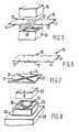
- Fig. 1 is a perspective view of a decal;
- Fig. 2 is a perspective view of the decal of Fig. 1, after moulding;
- Fig. 3 is a perspective view of a moulded substrate;
- Fig. 4 is a section on the line A-A of Fig. 3, prior to removal of the temporary carrier;
- Fig. 5 is a perspective view of a decal prior to insertion in a mould;
- Fig. 6 is a perspective view of the decal of Fig. 5, with a moulded-on substrate;
- Fig. 7 is a perspective view of the substrate of Fig. 6, with an embedded circuit;
- Fig. 8 is a perspective view of the substrate of Fig. 5, after post-forming;
- Fig. 9 is a perspective view of a patterned carrier;
- Fig. 10 is a section, on the line B-B of Fig. 9, of a substrate with a circuit embedded "face-down";
- Fig. 11 is a section, on the line B-B of Fig. 9, of a substrate with a circuit embedded "face-up";
- Fig. 12 is a section, on the line B-B of Fig. 9, of a substrate with circuits embedded both "face-down" and "face-up"; and
- Fig. 13 is a sectional sketch of a patterned carrier inserted in a mould cavity, prior to moulding the substrate of Fig. 12.
- As shown by Figs. 1 to 4, a decal 1 consists of a
circuit pattern 2 of electro-conductive or electro-resistive ink applied to aface 3 of a thin, flexible film 4 of insulating, thermo-formable material. The surface offace 3 is treated or otherwise formed so as to be able to release thecircuit pattern 2 and any moulding formed thereon, as described below. - Suitable inks are generally an epoxy resin base vehicle loaded with conductive or resistive material, such as silver powder or ferric oxide; e.g. Heraeus CERMALLOY (Trade Mark) CL80-5231. A suitable carrier material is General Electric ULTEM (Trade Mark) film, a thermoplastic polyetherimide. The CERMALLOY ink is screen printed on the ULTEM film and is left uncured; curing being effected by further processing. Alternatively, a thermoplastic ink may be employed.
- The decal is then formed, by any suitable thermo-forming technique, into the shape shown in Fig. 2. The formed decal is mounted on a mould core of complimentary shape (not shown), the decal and core are then inserted into a mould cavity and a component having the shape shown in Fig. 3 is then injection moulded onto the formed decal, the core supporting the non-patterned face of the decal during the moulding process; producing the component 5 shown in Fig. 4. Finally, the
temporary carrier 3 is stripped from the component moulding 5 to leave thecircuit 2 embedded in the inner surface 6 of the component. A suitable material for the component is Du Pont RYANITE (Trade Mark) FR 530 NC-10, a 30% glass-reinforced modified PETP, thermo-plastic polyester resin. Alternatively, and as described in more detail below, a non-release surface carrier may be provided and left bonded to the substrate. - Figs. 5 to 8 illustrate an alternative, continuous manufacturing process wherein a
decal 10, generally similar to decal 1 of the above-described embodiment, is employed; thisdecal 10 being acontinuous film 11 with marginal, indexingsprocket holes 12 and a series ofcircuit patterns 13 printed on the under, releaseface 14 of the film. For simplicity of illustration, thecircuit pattern 13 is shown to be an X, although more complex patterns would, in reality, be employed. In this embodiment, a suitable carrier film is Du Pont KAPTON (Trade Mark) film, a thermoset polyimide. - The decal film is shown in Fig. 1 to be indexed between the
top die 15 and the bottom die 16 of an injection mould, wherein a simple rectilinear moulding 17 (Fig. 6) is formed against theunderface 14 of the decal by thecavity 18 in thebottom die 16; the flat face (not shown) of thetop die 15 supporting the non-patterned face of the decal during the injection moulding process. Themould runner 19, formed by theinlet 20 to the mould cavity 18 (Fig. 1) at this stage remaining attached to themoulding 17. Thetemporary carrier film 11 is then removed to leave thecircuit 13 embedded in the moulding, flush with thesurface 21 thereof. - Thereafter the
moulding 17 is post-formed to any desired shape by conventional thermo-forming techniques; e.g. hot forming or vacuum moulding (both the circuit material and the moulding material are thermo-plastic). In the example illustrated by Fig. 8, themoulding 17 is inserted between a hotinternal punch 22, having a rectilinear shape, and a hot die 23, having acavity 24 of rectilinear shape complimentary to that ofpunch 22. Themoulding 17 is formed into an open toppedbox 25 having thecircuit 13 embedded in theinternal box surface 26. A suitable material for the moulding 17 again being RYANITE 530-NC10. - As shown by Fig. 9, a
circuit pattern 31 of electro-conductive and/or electro-resistive material is applied to oneface 32 of acarrier 33 in the form of a thin, flexible film of insulating material. Again, CERMALLOY ink is screen printed on to ULTEM film and left uncured. Alternatively, a thermo-plastic ink may be employed. - Fig. 10 shows one embodiment of substrate, with a circuit embedded "face-down", to consist of a
carrier 33 withapplied circuit pattern 31 and asubstrate 34 injection moulded onto thepatterned face 32 of the carrier; to leave thecircuit 31 embedded flush with thesurface 35 of the substrate and thecarrier 33 bonded to thesubstrate surface 35, to form an insulating cover for the circuit and substrate surface. The substrate is formed by inserting the patterned carrier in a mould cavity (not shown) with thenon-patterned face 36 supported by a surface of the mould cavity, so as to present the patterned face to the interior of the cavity. Insulating, thermo-plastic material is then injected into the mould cavity, the heat and pressure of the injection moulding process bonding the injected material to thecarrier surface 32 and around thecircuit 31. The circuit material, the carrier material and the substrate material all have to be compatible. A suitable substrate material, compatible with CERMALLOY ink and ULTEM film, is ULTEM resin, an amorphous thermo-plastic polyetherimide. - Fig. 11 shows another embodiment of substrate, but with the circuit embedded "face-up", this embodiment is generally similar to the Fig. 10 embodiment but it is produced by inserting the
carrier 33 into the mould cavity with the patternedface 32 supported by a surface of the mould cavity, so as to present thenon-patterned face 36 to the interior of the cavity. During injection moulding thecarrier 33 is shaped to conform to the three-dimensional shape of thecircuit 31 and the cavity surface so that the circuit becomes embedded in the carrier substantially flush with the outer face thereof; thesubstrate 34 bonding to theinner face 36 of the carrier. - Figs. 12 and 13 show a further embodiment of substrate, this time having circuits "face-down" and "face-up", wherein the
carrier 33 is provided with acircuit pattern 37 onface 36 in addition to thepattern 31 onface 32. The carrier is inserted in themould cavity 38 with its patternedface 32 supported by cavity surface 39. Resin material is injected into the cavity, as with the Fig. 10 and 11 embodiments, the heat and pressure created during the moulding process three-dimensionally shaping thecarrier 33 aboutcircuit 31, to embedcircuit 31 substantially flush with theouter face 32 of the carrier and embedcircuit 37 in thecarrier surface 35, beneath the shapedcarrier 33. - Clearly, by providing a compatible insulating interlayer, multi-layered "pairs" of circuits can be built up using this process.
- In an alternative, unillustrated moulding process, the embodiments of Figs. 10, 11 and 12 are produced by providing pre-moulded substrates of thermo-plastic material, laying the patterned carrier onto the substrate surface and applying heat and pressure (such as by a heated roller) to the carrier. Orientation of the patterned face of the carrier relative to the substrate determines whether circuits would be embedded "face-down" or "face-up". This method of moulding lends itself to a continuous process.
- Generally, carrier material has a higher melt temperature than the substrate material when the carrier is to be removed from the moulded substrate and of the same or similar melt temperature when the carrier is to be bonded to the substrate. The inks may be uncured thermo-set resins or thermo-plastic resins.
Claims (9)
- A method of embedding an electrical circuit in a plastics component to conform to three-dimensionally shaped surfaces thereof and comprising the steps of:-(i) providing a carrier, which is a thin, flexible film of insulating plastics material, with a circuit pattern of electro-conductive and/or electro-resistive synthetic, heat resistant resin material applied to at least one face thereof;(ii) inserting the patterned carrier in a mould cavity having a given three-dimensional shape, with a face of the carrier supported by the mould surface; and,(iii) charging the mould cavity with insulating plastics material to mould, by the application of heat and pressure, a substrate to fuse with the unsupported face of the carrier; whereby surfaces of the substrate and the embedded circuit pattern will conform to the shape of the mould.
- A method as claimed in Claim 1, wherein the patterned carrier is formed into a shape complementary to that of the formed carrier.
- A method as claimed in any of claims 1 or 2, wherein the non-patterned face of the carrier is supported; to produce a component with the circuit embedded in the substrate and the carrier fused with and covering the substrate surface.
- A method as claimed in any of claims 1 or 2, wherein the patterned face of the carrier is supported; to produce a component with the circuit embedded in and substantially flush with the surface of the carrier and with the carrier shaped about the circuit and fused with the substrate.
- A method as claimed in any of claims 1 or 2, wherein circuit patterns are applied to both faces of the carrier and one or the other patterned face is supported; to produce a component with one circuit embedded in and substantially flush with the surface of the carrier, the carrier shaped about said one circuit and fused with the substrate and the other circuit embedded in the substrate beneath the carrier.
- A method as claimed in any of Claims 1 to 5, wherein the melt temperature of the carrier material is the same or similar to the melt temperature of the substrate material, so that the carrier can fuse with the substrate.
- A method as claimed in any of Claims 1 to 5, wherein the carrier material, the circuit pattern material and the substrate material are all compatible so that they can fuse one with the other.
- A method as claimed in Claim 6 or Claim 7, wherein the carrier material is a thermoplastic polyetherimide; the circuit pattern material is an ink comprising an epoxy resin base vehicle loaded with conductive or resistive material and the substrate material is a glass-reinforced thermoplastic polyester resin.
- A method as claimed in Claim 8, wherein the circuit pattern is provided by printing the ink on to the carrier; the ink being left uncured, with curing being effected by further processing.
Priority Applications (1)
| Application Number | Priority Date | Filing Date | Title |
|---|---|---|---|
| AT86905344TATE83883T1 (en) | 1985-09-04 | 1986-09-03 | MANUFACTURE OF PRINTED CIRCUITS. |
Applications Claiming Priority (4)
| Application Number | Priority Date | Filing Date | Title |
|---|---|---|---|
| GB858522003AGB8522003D0 (en) | 1985-09-04 | 1985-09-04 | Printed circuits |
| GB8612116 | 1985-09-04 | ||
| GB868612116AGB8612116D0 (en) | 1986-05-19 | 1986-05-19 | Electrical circuits |
| GB8522003 | 1986-09-03 |
Publications (2)
| Publication Number | Publication Date |
|---|---|
| EP0236404A1 EP0236404A1 (en) | 1987-09-16 |
| EP0236404B1true EP0236404B1 (en) | 1992-12-23 |
Family
ID=26289730
Family Applications (1)
| Application Number | Title | Priority Date | Filing Date |
|---|---|---|---|
| EP86905344AExpired - LifetimeEP0236404B1 (en) | 1985-09-04 | 1986-09-03 | Manufacture of electrical circuits |
Country Status (7)
| Country | Link |
|---|---|
| US (2) | US4912288A (en) |
| EP (1) | EP0236404B1 (en) |
| JP (1) | JPH0712111B2 (en) |
| AT (1) | ATE83883T1 (en) |
| AU (1) | AU6285386A (en) |
| DE (1) | DE3687346T2 (en) |
| WO (1) | WO1987001557A1 (en) |
Cited By (1)
| Publication number | Priority date | Publication date | Assignee | Title |
|---|---|---|---|---|
| DE102010044598B3 (en)* | 2010-09-07 | 2012-01-19 | Leonhard Kurz Stiftung & Co. Kg | Antenna component and method for producing an antenna component |
Families Citing this family (90)
| Publication number | Priority date | Publication date | Assignee | Title |
|---|---|---|---|---|
| GB2193600B (en)* | 1986-07-11 | 1990-08-15 | Godfrey James Wright | Circuit component, and optical instrument incorporating the same |
| JPS6450497A (en)* | 1987-08-20 | 1989-02-27 | Satosen Co Ltd | Manufacture of printed wiring board |
| US4944087A (en)* | 1988-10-05 | 1990-07-31 | Rogers Corporation | Method of making a curved plastic body with circuit pattern |
| GB8824826D0 (en)* | 1988-10-24 | 1988-11-30 | Moran P | Moulded circuit board |
| US4985601A (en)* | 1989-05-02 | 1991-01-15 | Hagner George R | Circuit boards with recessed traces |
| FR2648305B1 (en)* | 1989-06-07 | 1993-03-26 | Peugeot | METHOD FOR MANUFACTURING A HOUSING FOR ELECTRONIC CIRCUIT AND HOUSING FOR ELECTRONIC CIRCUIT OBTAINED ACCORDING TO THIS METHOD, PARTICULARLY FOR MOTOR VEHICLE |
| JPH03147388A (en)* | 1989-10-23 | 1991-06-24 | Allen Bradley Internatl Ltd | Injection molding printed circuit |
| US5101319A (en)* | 1990-04-03 | 1992-03-31 | Vistatech Corporation | Pre-engineered electrode/dielectric composite film and related manufacturing process for multilayer ceramic chip capacitors |
| JP2747096B2 (en)* | 1990-07-24 | 1998-05-06 | 北川工業株式会社 | Method for manufacturing three-dimensional circuit board |
| US5096788A (en)* | 1990-10-05 | 1992-03-17 | Motorola, Inc. | Weldless battery pack |
| US5104754A (en)* | 1990-10-05 | 1992-04-14 | Motorola, Inc. | Weldless battery pack |
| DE4036592A1 (en)* | 1990-11-16 | 1992-05-21 | Bayer Ag | INJECTION MOLDED CIRCUITS BY INJECTING FLEXIBLE CIRCUITS WITH THERMOPLASTIC MATERIALS |
| JPH05251121A (en)* | 1991-12-18 | 1993-09-28 | Xerox Corp | Multi-layer wiring assembly |
| JP3342906B2 (en)* | 1991-12-18 | 2002-11-11 | ゼロックス・コーポレーション | Electronic device and electronic switch |
| US5298681A (en)* | 1992-04-20 | 1994-03-29 | Xerox Corporation | Frame member and assembly for carrying electrical signals and the like |
| US5455741A (en)* | 1993-10-26 | 1995-10-03 | Pulse Engineering, Inc. | Wire-lead through hole interconnect device |
| US5532518A (en)* | 1994-11-22 | 1996-07-02 | International Business Machines Corporation | Electrical connect and method of fabrication for semiconductor cube technology |
| US5835679A (en) | 1994-12-29 | 1998-11-10 | Energy Converters, Inc. | Polymeric immersion heating element with skeletal support and optional heat transfer fins |
| CH691020A5 (en)* | 1996-01-15 | 2001-03-30 | Fela Holding Ag | A process for the production of injection-molded three-dimensional circuit moldings. |
| US5620904A (en)* | 1996-03-15 | 1997-04-15 | Evergreen Solar, Inc. | Methods for forming wraparound electrical contacts on solar cells |
| US5741370A (en)* | 1996-06-27 | 1998-04-21 | Evergreen Solar, Inc. | Solar cell modules with improved backskin and methods for forming same |
| US5986203A (en)* | 1996-06-27 | 1999-11-16 | Evergreen Solar, Inc. | Solar cell roof tile and method of forming same |
| US5762720A (en)* | 1996-06-27 | 1998-06-09 | Evergreen Solar, Inc. | Solar cell modules with integral mounting structure and methods for forming same |
| DE69729030T2 (en)* | 1996-07-15 | 2004-09-09 | Matsushita Electric Industrial Co., Ltd., Kadoma | Dielectric multilayer device and associated manufacturing process |
| US6005463A (en)* | 1997-01-30 | 1999-12-21 | Pulse Engineering | Through-hole interconnect device with isolated wire-leads and component barriers |
| US6278053B1 (en) | 1997-03-25 | 2001-08-21 | Evergreen Solar, Inc. | Decals and methods for providing an antireflective coating and metallization on a solar cell |
| US6114046A (en)* | 1997-07-24 | 2000-09-05 | Evergreen Solar, Inc. | Encapsulant material for solar cell module and laminated glass applications |
| US6187448B1 (en) | 1997-07-24 | 2001-02-13 | Evergreen Solar, Inc. | Encapsulant material for solar cell module and laminated glass applications |
| US6320116B1 (en) | 1997-09-26 | 2001-11-20 | Evergreen Solar, Inc. | Methods for improving polymeric materials for use in solar cell applications |
| DE19812880A1 (en)* | 1998-03-24 | 1999-09-30 | Bayer Ag | Shaped part and flexible film with protected conductor track and process for its production |
| US6263158B1 (en) | 1999-05-11 | 2001-07-17 | Watlow Polymer Technologies | Fibrous supported polymer encapsulated electrical component |
| US6395983B1 (en) | 1999-05-18 | 2002-05-28 | Pulse Engineering, Inc. | Electronic packaging device and method |
| US6392208B1 (en) | 1999-08-06 | 2002-05-21 | Watlow Polymer Technologies | Electrofusing of thermoplastic heating elements and elements made thereby |
| US8398413B2 (en) | 2000-02-07 | 2013-03-19 | Micro Contacts, Inc. | Carbon fiber electrical contacts formed of composite material including plural carbon fiber elements bonded together in low-resistance synthetic resin |
| US6444102B1 (en) | 2000-02-07 | 2002-09-03 | Micro Contacts Inc. | Carbon fiber electrical contacts |
| US8029296B2 (en)* | 2000-02-07 | 2011-10-04 | Micro Contacts, Inc. | Carbon fiber electrical contacts formed of composite carbon fiber material |
| US6433317B1 (en) | 2000-04-07 | 2002-08-13 | Watlow Polymer Technologies | Molded assembly with heating element captured therein |
| US6519835B1 (en) | 2000-08-18 | 2003-02-18 | Watlow Polymer Technologies | Method of formable thermoplastic laminate heated element assembly |
| US6539171B2 (en) | 2001-01-08 | 2003-03-25 | Watlow Polymer Technologies | Flexible spirally shaped heating element |
| US7041159B2 (en)* | 2003-08-04 | 2006-05-09 | Phillips Plastics Corporation | Separation apparatus |
| US20040139858A1 (en)* | 2001-03-01 | 2004-07-22 | Phillips Plastics Corporation | Filtration media of porous inorganic particles |
| WO2002070105A2 (en) | 2001-03-01 | 2002-09-12 | Phillips Plastics Corporation | Filtration media of porous inorganic particles |
| DE10118487A1 (en)* | 2001-04-12 | 2002-10-17 | Demag Ergotech Gmbh | Plastic component with electrical functions, e.g. a chip card, contains functional elements, e.g. an antenna, made of electrically conducting plastic |
| US6797041B2 (en)* | 2002-03-01 | 2004-09-28 | Greenheck Fan Corporation | Two stage air filter |
| US7166140B2 (en)* | 2003-10-22 | 2007-01-23 | Phillips Plastics Corporation | High capture efficiency baffle |
| GB2412247B (en)* | 2004-03-16 | 2007-08-22 | In2Tec Ltd | Contoured circuit boards |
| DE102005034082A1 (en)* | 2005-07-21 | 2007-02-01 | Hirschmann Car Communication Gmbh | Method for applying electrical conductor structures to a target component made of plastic |
| US8048510B2 (en) | 2005-09-21 | 2011-11-01 | Whirlpool Corporation | Liner with electrical pathways |
| EP2030248A2 (en)* | 2006-06-21 | 2009-03-04 | Evergreen Solar, Inc. | Frameless photovoltaic module |
| US8007704B2 (en)* | 2006-07-20 | 2011-08-30 | Honeywell International Inc. | Insert molded actuator components |
| EP2092572A1 (en)* | 2006-12-15 | 2009-08-26 | Evergreen Solar, Inc. | Plug-together photovoltaic modules |
| JP2010521822A (en)* | 2007-03-14 | 2010-06-24 | エバーグリーン ソーラー, インコーポレイテッド | Solar cell module having stiffening layer |
| US8238073B2 (en)* | 2008-07-18 | 2012-08-07 | Synaptics, Inc. | In-molded capacitive sensors |
| US8325047B2 (en) | 2009-04-08 | 2012-12-04 | Sabic Innovative Plastics Ip B.V. | Encapsulated RFID tags and methods of making same |
| US11090104B2 (en) | 2009-10-09 | 2021-08-17 | Cilag Gmbh International | Surgical generator for ultrasonic and electrosurgical devices |
| DE102011014902B3 (en)* | 2011-03-23 | 2012-02-02 | Leonhard Kurz Stiftung & Co. Kg | Producing an antenna component with a three-dimensional antenna, comprises forming an electrical conductive layer made of an electrical conductive lacquer onto a thermoplastic carrier foil in an antenna area formed as antenna structure |
| KR101214671B1 (en)* | 2011-10-27 | 2012-12-21 | 삼성전기주식회사 | Printed circuit board comprising embedded electronic component within and method of manufacturing the same |
| DE102011117985B8 (en)* | 2011-11-09 | 2016-12-01 | Leonhard Kurz Stiftung & Co. Kg | Plastic part and method for producing a plastic part |
| US20130240252A1 (en)* | 2012-03-19 | 2013-09-19 | Taiwan Green Point Enterprises Co., Ltd | 3d-shaped component with a circuit trace pattern and method for making the same |
| US9408622B2 (en) | 2012-06-29 | 2016-08-09 | Ethicon Endo-Surgery, Llc | Surgical instruments with articulating shafts |
| US8914875B2 (en) | 2012-10-26 | 2014-12-16 | Facebook, Inc. | Contextual device locking/unlocking |
| EP3020258A1 (en) | 2013-07-09 | 2016-05-18 | Koninklijke Philips N.V. | Method for manufacturing a printed circuit board assembly based on printed electronics and printed circuit board assembly |
| KR102444269B1 (en) | 2013-09-27 | 2022-09-16 | 택토텍 오와이 | A method for manufacturing the structure of an electric machine and an arrangement for carrying out the method |
| WO2015101494A1 (en)* | 2014-01-02 | 2015-07-09 | Koninklijke Philips N.V. | Method for manufacturing a non-planar printed circuit board assembly |
| JP6794091B2 (en)* | 2014-12-12 | 2020-12-02 | 凸版印刷株式会社 | Wiring printed matter manufacturing method |
| US10426037B2 (en) | 2015-07-15 | 2019-09-24 | International Business Machines Corporation | Circuitized structure with 3-dimensional configuration |
| US11129670B2 (en) | 2016-01-15 | 2021-09-28 | Cilag Gmbh International | Modular battery powered handheld surgical instrument with selective application of energy based on button displacement, intensity, or local tissue characterization |
| US11051840B2 (en) | 2016-01-15 | 2021-07-06 | Ethicon Llc | Modular battery powered handheld surgical instrument with reusable asymmetric handle housing |
| US11229471B2 (en) | 2016-01-15 | 2022-01-25 | Cilag Gmbh International | Modular battery powered handheld surgical instrument with selective application of energy based on tissue characterization |
| US12193698B2 (en) | 2016-01-15 | 2025-01-14 | Cilag Gmbh International | Method for self-diagnosing operation of a control switch in a surgical instrument system |
| US10555769B2 (en)* | 2016-02-22 | 2020-02-11 | Ethicon Llc | Flexible circuits for electrosurgical instrument |
| US11266430B2 (en) | 2016-11-29 | 2022-03-08 | Cilag Gmbh International | End effector control and calibration |
| DE102018120711A1 (en)* | 2018-08-24 | 2020-02-27 | Airbus India Operations Private Limited | Method and device for producing a composite material component with an integrated electrical conductor circuit and composite material component obtainable therewith |
| US10856365B2 (en) | 2018-11-14 | 2020-12-01 | Mark Allen Ester | Self regulating flexible heating device |
| WO2020218326A1 (en)* | 2019-04-23 | 2020-10-29 | 京セラ株式会社 | Wiring board, electronic device, and electronic module |
| FI130084B (en)* | 2019-12-13 | 2023-01-31 | Canatu Oy | A formed film and a method for manufacturing thereof |
| US20210196357A1 (en) | 2019-12-30 | 2021-07-01 | Ethicon Llc | Electrosurgical instrument with asynchronous energizing electrodes |
| US12076006B2 (en) | 2019-12-30 | 2024-09-03 | Cilag Gmbh International | Surgical instrument comprising an orientation detection system |
| US12053224B2 (en) | 2019-12-30 | 2024-08-06 | Cilag Gmbh International | Variation in electrode parameters and deflectable electrode to modify energy density and tissue interaction |
| US11812957B2 (en) | 2019-12-30 | 2023-11-14 | Cilag Gmbh International | Surgical instrument comprising a signal interference resolution system |
| US12343063B2 (en) | 2019-12-30 | 2025-07-01 | Cilag Gmbh International | Multi-layer clamp arm pad for enhanced versatility and performance of a surgical device |
| US11937866B2 (en) | 2019-12-30 | 2024-03-26 | Cilag Gmbh International | Method for an electrosurgical procedure |
| US12262937B2 (en) | 2019-12-30 | 2025-04-01 | Cilag Gmbh International | User interface for surgical instrument with combination energy modality end-effector |
| US12023086B2 (en) | 2019-12-30 | 2024-07-02 | Cilag Gmbh International | Electrosurgical instrument for delivering blended energy modalities to tissue |
| US11950797B2 (en) | 2019-12-30 | 2024-04-09 | Cilag Gmbh International | Deflectable electrode with higher distal bias relative to proximal bias |
| US11937863B2 (en) | 2019-12-30 | 2024-03-26 | Cilag Gmbh International | Deflectable electrode with variable compression bias along the length of the deflectable electrode |
| US11986201B2 (en) | 2019-12-30 | 2024-05-21 | Cilag Gmbh International | Method for operating a surgical instrument |
| US12336747B2 (en) | 2019-12-30 | 2025-06-24 | Cilag Gmbh International | Method of operating a combination ultrasonic / bipolar RF surgical device with a combination energy modality end-effector |
| US11786294B2 (en) | 2019-12-30 | 2023-10-17 | Cilag Gmbh International | Control program for modular combination energy device |
| JP7035099B2 (en) | 2020-01-28 | 2022-03-14 | Nissha株式会社 | Three-dimensional molded product with circuit and its manufacturing method |
Family Cites Families (28)
| Publication number | Priority date | Publication date | Assignee | Title |
|---|---|---|---|---|
| GB656259A (en)* | 1940-09-06 | 1951-08-15 | Oxvar Ltd | Improvements in the manufacture of decorated articles |
| BE514138A (en)* | 1951-09-14 | |||
| GB715207A (en)* | 1951-10-11 | 1954-09-08 | Hunt Capacitors Ltd A | Improvements in or relating to electric circuits and circuit components |
| NL190034A (en)* | 1953-08-17 | |||
| US2972003A (en)* | 1956-02-21 | 1961-02-14 | Rogers Corp | Printed circuits and methods of making the same |
| GB822826A (en)* | 1956-10-22 | 1959-11-04 | St Regis Paper Co | Printed circuitry laminates and production thereof |
| US3039177A (en)* | 1957-07-29 | 1962-06-19 | Itt | Multiplanar printed circuit |
| US3024151A (en)* | 1957-09-30 | 1962-03-06 | Automated Circuits Inc | Printed electrical circuits and method of making the same |
| US3161945A (en)* | 1958-05-21 | 1964-12-22 | Rogers Corp | Method of making a printed circuit |
| US3059320A (en)* | 1958-06-23 | 1962-10-23 | Ibm | Method of making electrical circuit |
| US3077658A (en)* | 1960-04-11 | 1963-02-19 | Gen Dynamics Corp | Method of manufacturing molded module assemblies |
| US3181986A (en)* | 1961-03-31 | 1965-05-04 | Intellux Inc | Method of making inlaid circuits |
| GB984250A (en)* | 1962-01-08 | 1965-02-24 | Avisun Corp | Method of moulding plastics articles and articles made by such method |
| DE1243746B (en)* | 1965-05-15 | 1967-07-06 | Telefunken Patent | Process for the production of a printed circuit on a carrier plate, the surface of which deviates from a plane |
| JPS5026577B1 (en)* | 1966-11-19 | 1975-09-02 | ||
| GB1276095A (en)* | 1968-09-05 | 1972-06-01 | Secr Defence | Microcircuits and processes for their manufacture |
| US3678577A (en)* | 1969-09-25 | 1972-07-25 | Jerobee Ind Inc | Method of contemporaneously shearing and bonding conductive foil to a substrate |
| US4050976A (en)* | 1976-01-27 | 1977-09-27 | Bofors America, Inc. | Strain gage application |
| US4301580A (en)* | 1977-04-16 | 1981-11-24 | Wallace Clarence L | Manufacture of multi-layered electrical assemblies |
| JPS5412459A (en)* | 1977-06-30 | 1979-01-30 | Olympus Optical Co | Substrate device for electronic apparatus and method of manufacturing same |
| JPS55128897A (en)* | 1979-03-27 | 1980-10-06 | Citizen Watch Co Ltd | Circuit board for watch and methdo of fabricating same |
| US4407685A (en)* | 1979-07-23 | 1983-10-04 | Ford Aerospace & Communication Corporation | Metallized film transfer process |
| US4369557A (en)* | 1980-08-06 | 1983-01-25 | Jan Vandebult | Process for fabricating resonant tag circuit constructions |
| JPS58151094A (en)* | 1982-03-02 | 1983-09-08 | 日立化成工業株式会社 | Method of producing flexible printed circuit board with reinforcing material |
| US4545752A (en)* | 1982-08-17 | 1985-10-08 | Dai Nippon Insatsu Kabushiki Kaisha | Device for injection molding articles while simultaneously forming patterns thereon |
| US4415607A (en)* | 1982-09-13 | 1983-11-15 | Allen-Bradley Company | Method of manufacturing printed circuit network devices |
| US4710419A (en)* | 1984-07-16 | 1987-12-01 | Gregory Vernon C | In-mold process for fabrication of molded plastic printed circuit boards |
| US4584767A (en)* | 1984-07-16 | 1986-04-29 | Gregory Vernon C | In-mold process for fabrication of molded plastic printed circuit boards |
- 1986
- 1986-09-03EPEP86905344Apatent/EP0236404B1/ennot_activeExpired - Lifetime
- 1986-09-03DEDE8686905344Tpatent/DE3687346T2/ennot_activeExpired - Fee Related
- 1986-09-03ATAT86905344Tpatent/ATE83883T1/ennot_activeIP Right Cessation
- 1986-09-03USUS07/071,267patent/US4912288A/ennot_activeExpired - Lifetime
- 1986-09-03WOPCT/GB1986/000523patent/WO1987001557A1/enactiveIP Right Grant
- 1986-09-03JPJP61504631Apatent/JPH0712111B2/ennot_activeExpired - Fee Related
- 1986-09-03AUAU62853/86Apatent/AU6285386A/ennot_activeAbandoned
- 1989
- 1989-09-11USUS07/443,402patent/US5003693A/ennot_activeExpired - Lifetime
Cited By (1)
| Publication number | Priority date | Publication date | Assignee | Title |
|---|---|---|---|---|
| DE102010044598B3 (en)* | 2010-09-07 | 2012-01-19 | Leonhard Kurz Stiftung & Co. Kg | Antenna component and method for producing an antenna component |
Also Published As
| Publication number | Publication date |
|---|---|
| DE3687346D1 (en) | 1993-02-04 |
| WO1987001557A1 (en) | 1987-03-12 |
| AU6285386A (en) | 1987-03-24 |
| JPS63500758A (en) | 1988-03-17 |
| DE3687346T2 (en) | 1993-04-22 |
| JPH0712111B2 (en) | 1995-02-08 |
| EP0236404A1 (en) | 1987-09-16 |
| US4912288A (en) | 1990-03-27 |
| US5003693A (en) | 1991-04-02 |
| ATE83883T1 (en) | 1993-01-15 |
Similar Documents
| Publication | Publication Date | Title |
|---|---|---|
| EP0236404B1 (en) | Manufacture of electrical circuits | |
| EP0389619B1 (en) | Method of making a curved plastic body with circuit pattern | |
| US5738797A (en) | Three-dimensional multi-layer circuit structure and method for forming the same | |
| US5220488A (en) | Injection molded printed circuits | |
| US4710419A (en) | In-mold process for fabrication of molded plastic printed circuit boards | |
| EP0424796A2 (en) | Injection molded printed circuits | |
| GB2266410A (en) | Circuit parts including conductor patterns on moulded bases | |
| EP0358504A3 (en) | Electrical components | |
| JPS60121791A (en) | Method of producing printed circuit board | |
| JPH0439011A (en) | Composite printed wiring board and its manufacture | |
| JPH0527999B2 (en) | ||
| JPH04221879A (en) | Printed circuit board with jumper section and manufacturing method thereof | |
| JPH0541574A (en) | Manufacture of printed circuit board | |
| JP2810858B2 (en) | Circuit board and its manufacturing method | |
| JPH01266789A (en) | Manufacture of molded circuit board | |
| JPH04239795A (en) | Fabrication of injection molded circuit parts | |
| JP2687314B2 (en) | Circuit board and its manufacturing method | |
| JPH0756906B2 (en) | Circuit board | |
| JPH02288294A (en) | Manufacture of circuit substrate | |
| JPS62280018A (en) | Transfer material for printed-wiring board and printed-wiring board made of said transfer material and manufacture thereof | |
| JPH0563035B2 (en) | ||
| JPS63257293A (en) | Method for manufacturing a molded product having a printed circuit and transfer sheet used for manufacturing the same | |
| JPH0563111B2 (en) | ||
| JPH0726858Y2 (en) | Printed circuit board | |
| JPS62237798A (en) | Resin case for electronic equipment |
Legal Events
| Date | Code | Title | Description |
|---|---|---|---|
| PUAI | Public reference made under article 153(3) epc to a published international application that has entered the european phase | Free format text:ORIGINAL CODE: 0009012 | |
| 17P | Request for examination filed | Effective date:19870429 | |
| AK | Designated contracting states | Kind code of ref document:A1 Designated state(s):AT BE CH DE FR GB IT LI LU NL SE | |
| 17Q | First examination report despatched | Effective date:19890711 | |
| GRAA | (expected) grant | Free format text:ORIGINAL CODE: 0009210 | |
| RAP1 | Party data changed (applicant data changed or rights of an application transferred) | Owner name:UFE, INC. | |
| AK | Designated contracting states | Kind code of ref document:B1 Designated state(s):AT BE CH DE FR GB IT LI LU NL SE | |
| REF | Corresponds to: | Ref document number:83883 Country of ref document:AT Date of ref document:19930115 Kind code of ref document:T | |
| RIN1 | Information on inventor provided before grant (corrected) | Inventor name:DENES, OSCAR L. Inventor name:GRAY, RICHARD Inventor name:ATKINSON, ANTHONY | |
| ET | Fr: translation filed | ||
| ITF | It: translation for a ep patent filed | ||
| REF | Corresponds to: | Ref document number:3687346 Country of ref document:DE Date of ref document:19930204 | |
| ITTA | It: last paid annual fee | ||
| PG25 | Lapsed in a contracting state [announced via postgrant information from national office to epo] | Ref country code:LU Free format text:LAPSE BECAUSE OF NON-PAYMENT OF DUE FEES Effective date:19930930 | |
| PLBE | No opposition filed within time limit | Free format text:ORIGINAL CODE: 0009261 | |
| STAA | Information on the status of an ep patent application or granted ep patent | Free format text:STATUS: NO OPPOSITION FILED WITHIN TIME LIMIT | |
| 26N | No opposition filed | ||
| EAL | Se: european patent in force in sweden | Ref document number:86905344.7 | |
| PGFP | Annual fee paid to national office [announced via postgrant information from national office to epo] | Ref country code:SE Payment date:20010806 Year of fee payment:16 | |
| PGFP | Annual fee paid to national office [announced via postgrant information from national office to epo] | Ref country code:GB Payment date:20010807 Year of fee payment:16 | |
| PGFP | Annual fee paid to national office [announced via postgrant information from national office to epo] | Ref country code:FR Payment date:20010816 Year of fee payment:16 | |
| PGFP | Annual fee paid to national office [announced via postgrant information from national office to epo] | Ref country code:BE Payment date:20010907 Year of fee payment:16 | |
| PGFP | Annual fee paid to national office [announced via postgrant information from national office to epo] | Ref country code:AT Payment date:20010918 Year of fee payment:16 | |
| PGFP | Annual fee paid to national office [announced via postgrant information from national office to epo] | Ref country code:CH Payment date:20010928 Year of fee payment:16 | |
| PGFP | Annual fee paid to national office [announced via postgrant information from national office to epo] | Ref country code:NL Payment date:20010930 Year of fee payment:16 | |
| REG | Reference to a national code | Ref country code:GB Ref legal event code:IF02 | |
| PG25 | Lapsed in a contracting state [announced via postgrant information from national office to epo] | Ref country code:GB Free format text:LAPSE BECAUSE OF NON-PAYMENT OF DUE FEES Effective date:20020903 Ref country code:AT Free format text:LAPSE BECAUSE OF NON-PAYMENT OF DUE FEES Effective date:20020903 | |
| PG25 | Lapsed in a contracting state [announced via postgrant information from national office to epo] | Ref country code:SE Free format text:LAPSE BECAUSE OF NON-PAYMENT OF DUE FEES Effective date:20020904 | |
| PG25 | Lapsed in a contracting state [announced via postgrant information from national office to epo] | Ref country code:LI Free format text:LAPSE BECAUSE OF NON-PAYMENT OF DUE FEES Effective date:20020930 Ref country code:CH Free format text:LAPSE BECAUSE OF NON-PAYMENT OF DUE FEES Effective date:20020930 Ref country code:BE Free format text:LAPSE BECAUSE OF NON-PAYMENT OF DUE FEES Effective date:20020930 | |
| BERE | Be: lapsed | Owner name:*UFE INC. Effective date:20020930 | |
| PG25 | Lapsed in a contracting state [announced via postgrant information from national office to epo] | Ref country code:NL Free format text:LAPSE BECAUSE OF NON-PAYMENT OF DUE FEES Effective date:20030401 | |
| GBPC | Gb: european patent ceased through non-payment of renewal fee | Effective date:20020903 | |
| EUG | Se: european patent has lapsed | ||
| REG | Reference to a national code | Ref country code:CH Ref legal event code:PL | |
| PG25 | Lapsed in a contracting state [announced via postgrant information from national office to epo] | Ref country code:FR Free format text:LAPSE BECAUSE OF NON-PAYMENT OF DUE FEES Effective date:20030603 | |
| REG | Reference to a national code | Ref country code:FR Ref legal event code:ST | |
| PGFP | Annual fee paid to national office [announced via postgrant information from national office to epo] | Ref country code:DE Payment date:20031028 Year of fee payment:18 | |
| PG25 | Lapsed in a contracting state [announced via postgrant information from national office to epo] | Ref country code:DE Free format text:LAPSE BECAUSE OF NON-PAYMENT OF DUE FEES Effective date:20050401 | |
| PG25 | Lapsed in a contracting state [announced via postgrant information from national office to epo] | Ref country code:IT Free format text:LAPSE BECAUSE OF NON-PAYMENT OF DUE FEES;WARNING: LAPSES OF ITALIAN PATENTS WITH EFFECTIVE DATE BEFORE 2007 MAY HAVE OCCURRED AT ANY TIME BEFORE 2007. THE CORRECT EFFECTIVE DATE MAY BE DIFFERENT FROM THE ONE RECORDED. Effective date:20050903 |