EP0235770B1 - Device for the plasma processing of substrates in a high frequency excited plasma discharge - Google Patents
Device for the plasma processing of substrates in a high frequency excited plasma dischargeDownload PDFInfo
- Publication number
- EP0235770B1 EP0235770B1EP87102866AEP87102866AEP0235770B1EP 0235770 B1EP0235770 B1EP 0235770B1EP 87102866 AEP87102866 AEP 87102866AEP 87102866 AEP87102866 AEP 87102866AEP 0235770 B1EP0235770 B1EP 0235770B1
- Authority
- EP
- European Patent Office
- Prior art keywords
- electrode
- hollow anode
- hollow
- substrate
- substrates
- Prior art date
- Legal status (The legal status is an assumption and is not a legal conclusion. Google has not performed a legal analysis and makes no representation as to the accuracy of the status listed.)
- Expired - Lifetime
Links
- 239000000758substrateSubstances0.000titleclaimsabstractdescription82
- 230000008878couplingEffects0.000claimsdescription22
- 238000010168coupling processMethods0.000claimsdescription22
- 238000005859coupling reactionMethods0.000claimsdescription22
- 239000007789gasSubstances0.000claimsdescription14
- 238000012216screeningMethods0.000claims1
- 238000009832plasma treatmentMethods0.000abstractdescription5
- 239000011796hollow space materialSubstances0.000abstractdescription3
- 239000010410layerSubstances0.000description11
- 230000015572biosynthetic processEffects0.000description6
- 239000007795chemical reaction productSubstances0.000description3
- 238000000151depositionMethods0.000description3
- 230000008021depositionEffects0.000description3
- 238000009826distributionMethods0.000description3
- 230000000694effectsEffects0.000description3
- 238000005530etchingMethods0.000description3
- 239000000463materialSubstances0.000description3
- 239000002184metalSubstances0.000description3
- 229910052751metalInorganic materials0.000description3
- RYGMFSIKBFXOCR-UHFFFAOYSA-NCopperChemical compound[Cu]RYGMFSIKBFXOCR-UHFFFAOYSA-N0.000description2
- 229910003481amorphous carbonInorganic materials0.000description2
- 239000003990capacitorSubstances0.000description2
- 238000001816coolingMethods0.000description2
- 238000013461designMethods0.000description2
- 150000002500ionsChemical class0.000description2
- 238000000034methodMethods0.000description2
- 229920000642polymerPolymers0.000description2
- 238000006116polymerization reactionMethods0.000description2
- 230000008569processEffects0.000description2
- 230000000717retained effectEffects0.000description2
- 238000011282treatmentMethods0.000description2
- 239000004215Carbon black (E152)Substances0.000description1
- UFHFLCQGNIYNRP-UHFFFAOYSA-NHydrogenChemical compound[H][H]UFHFLCQGNIYNRP-UHFFFAOYSA-N0.000description1
- 230000004913activationEffects0.000description1
- 239000012300argon atmosphereSubstances0.000description1
- 230000008901benefitEffects0.000description1
- 238000005266castingMethods0.000description1
- 230000008859changeEffects0.000description1
- 239000011248coating agentSubstances0.000description1
- 238000000576coating methodMethods0.000description1
- 230000000295complement effectEffects0.000description1
- 238000002474experimental methodMethods0.000description1
- 229930195733hydrocarbonNatural products0.000description1
- 150000002430hydrocarbonsChemical class0.000description1
- 239000001257hydrogenSubstances0.000description1
- 229910052739hydrogenInorganic materials0.000description1
- 238000004519manufacturing processMethods0.000description1
- 239000007769metal materialSubstances0.000description1
- 238000012986modificationMethods0.000description1
- 230000004048modificationEffects0.000description1
- 230000003287optical effectEffects0.000description1
- 239000002245particleSubstances0.000description1
- 238000001020plasma etchingMethods0.000description1
- 239000011241protective layerSubstances0.000description1
- 239000007787solidSubstances0.000description1
- 238000004544sputter depositionMethods0.000description1
- 230000003068static effectEffects0.000description1
- 238000012360testing methodMethods0.000description1
- 238000002834transmittanceMethods0.000description1
- 238000004804windingMethods0.000description1
Images


Classifications
- H—ELECTRICITY
- H01—ELECTRIC ELEMENTS
- H01J—ELECTRIC DISCHARGE TUBES OR DISCHARGE LAMPS
- H01J37/00—Discharge tubes with provision for introducing objects or material to be exposed to the discharge, e.g. for the purpose of examination or processing thereof
- H01J37/32—Gas-filled discharge tubes
- H01J37/32009—Arrangements for generation of plasma specially adapted for examination or treatment of objects, e.g. plasma sources
- B—PERFORMING OPERATIONS; TRANSPORTING
- B29—WORKING OF PLASTICS; WORKING OF SUBSTANCES IN A PLASTIC STATE IN GENERAL
- B29C—SHAPING OR JOINING OF PLASTICS; SHAPING OF MATERIAL IN A PLASTIC STATE, NOT OTHERWISE PROVIDED FOR; AFTER-TREATMENT OF THE SHAPED PRODUCTS, e.g. REPAIRING
- B29C59/00—Surface shaping of articles, e.g. embossing; Apparatus therefor
- B29C59/14—Surface shaping of articles, e.g. embossing; Apparatus therefor by plasma treatment
- H—ELECTRICITY
- H01—ELECTRIC ELEMENTS
- H01J—ELECTRIC DISCHARGE TUBES OR DISCHARGE LAMPS
- H01J37/00—Discharge tubes with provision for introducing objects or material to be exposed to the discharge, e.g. for the purpose of examination or processing thereof
- H01J37/32—Gas-filled discharge tubes
- H01J37/32009—Arrangements for generation of plasma specially adapted for examination or treatment of objects, e.g. plasma sources
- H01J37/32082—Radio frequency generated discharge
- H—ELECTRICITY
- H01—ELECTRIC ELEMENTS
- H01J—ELECTRIC DISCHARGE TUBES OR DISCHARGE LAMPS
- H01J37/00—Discharge tubes with provision for introducing objects or material to be exposed to the discharge, e.g. for the purpose of examination or processing thereof
- H01J37/32—Gas-filled discharge tubes
- H01J37/32431—Constructional details of the reactor
- H01J37/32532—Electrodes
- H01J37/32541—Shape
Definitions
- the inventionrelates to a device for the plasma treatment of substrates in a plasma discharge excited by high frequency between two electrodes supplied by a high frequency source, of which the first is designed as a hollow anode and the second electrode carrying the substrate is arranged in front of the cavity of the anode or can be guided past it.
- the hollow anodeis drawn in the direction of the second electrode, at the same potential as the hollow anode edge, which forms a gap "s 1" of a maximum of 10 mm in width on all sides with respect to the second electrode.
- the plasma treatment for which the device is intendedcan be plasma etching, the production of polymer layers on the substrates by plasma polymerization, the activation of substrate surfaces, etc.
- Devices for the plasma treatment of substrates by means of high frequencyusually contain two electrodes, one of which is formed by the vacuum chamber and / or by the substrate holder, both of which are made of metallic materials. It is known that a voltage which is predominantly negative with respect to the plasma and which has the smaller effective surface with respect to the surfaces acting as counterelectrode is formed in each case on that electrode.
- the negatively biased electrodeis therefore also referred to here regularly as the "cathode".
- the polarity of the electrodesis mandatory due to their connection to the respective pole of the DC voltage source.
- DE-OS 21 15 590it is known, for example, to use a hollow cathode with an edge projecting in the direction of the substrate carrier in order to improve the uniformity of the layer thickness distribution.
- this protruding edgedoes not lead to a reversal of the polarity when using DC voltage.
- the known solutionleads to some difficulties when using this principle in certain devices with continuous substrate transport: namely, if the substrate holder with the substrate is removed, at least the metallic base plate of the vacuum chamber, which generally has a larger area than that, acts as the counter electrode has a hollow electrode and is connected to ground. In this case, the negative voltage on the hollow electrode, which now acts as a cathode, forms in a complete reversal of the potential relationships.
- the size of the gap between the edge of the hollow electrode on the one hand and the substrate or substrate holder on the other handis of essential importance for the formation of the potential distribution in the area of the space filled by the plasma. Since the gap mentioned represents the connection of the plasma to its surroundings, the gap size decides whether the hollow electrode acts as an anode or as a cathode of the arrangement. Experiments have shown that increasing the gap above an amount of about 1 mm dramatically increases the influence of the other metallic parts of the device, with the consequence of the formation of a negative bias on the hollow electrode instead of on the substrate.
- the inventionis therefore based on the object of improving a device of the type described at the outset in such a way that it is less sensitive to an increase in the gap and in particular can also be used in devices with continuous or quasi-continuous substrate transport, i.e. in so-called "in-line systems".
- the objectis achieved in the device specified at the outset according to the invention in that in the cavity of the hollow anode on its interior Surface enlarging projections are arranged.
- the surface of the hollow anode facing the plasmais considerably enlarged, so that the plasma weft is retained even with a noticeable increase in the gap width and there is still no reversal of the potential relationships when mobile or displaceable substrate holders are transported relative to the opening of the hollow anode.
- the geometric shape of the protrusionsis not critical; they should only bring about the greatest possible surface enlargement, although the spacing of the projections from one another or the cavities formed between the projections and the edge must not be dimensioned so small that the surface enlargement would be ineffective with respect to the plasma. The distances must therefore not be less than twice the so-called "dark room distance".
- the increase in the inner surface of the hollow anoderesults in an increase in the negative voltage which forms on the surface of the substrate or the substrate holder relative to the hollow anode. This results in a corresponding increase in the kinetic energy of the positively charged ions striking the substrate from the plasma space.
- the device according to the inventionis used as an etching device, this leads to an increase in the specific etching rate.
- the bombardment of the layer growing on the substrate with positive ionsleads to particularly high-quality layers because of the simultaneous sputtering off of the weakly bound particles of the layer.
- the properties of the hollow anodeare fully retained even when the substrate is being transported: the plasma is completely enclosed by material walls, in contrast to, for example, an inclusion by magnetic fields, which is never complete, especially when high frequency is used. Furthermore, through the complete containment by the hollow anode reached a plasma density in the plasma space that cannot be achieved with plasma confinement by means of magnetic fields, provided comparable electrical powers per unit area. In addition, studies have shown that the plasma density in the entire hollow space of the hollow anode, with the exception of a decrease in the immediate edge area, is so uniform that a deviation cannot be observed optically. The drop in plasma density in the edge area is limited to less than 5 mm. This leads to deviations in the layer thickness which are smaller than ⁇ 3%, a value which cannot be achieved with magnetic confinement of the plasma.
- the formation of the anode according to the inventionis easy to carry out, namely by a casting process or by a composition of metallic strip material.
- the hollow anode according to the inventioncan also be easily exchanged for one according to the prior art without the need for laborious modifications to the entire device.
- the device according to the inventionis suitable for plasma polymerization, ie for the deposition of polymer layers on the substrates, but in particular for the deposition of amorphous carbon as a protective layer on substrates.
- a gaseous hydrocarbonis introduced into the cavity of the hollow anode, the reaction products (mainly hydrogen) being removed in ways described in more detail below.
- the edge of the dark room shieldforms a gap "s2" of a maximum of 10 mm on all sides with respect to the second electrode (the substrate holder).
- Such a devicecan, according to the yet further embodiment of the invention, be additionally characterized in that electrical coupling elements are arranged on at least part of the circumference of the dark room shielding, which run essentially parallel to the adjacent surface of the second electrode at a distance from the gap "s2". Coupling elements of this type have the additional advantage that the gap "s 1" can be dimensioned even larger before the "edge effect" disappears.
- the substrate holderwas by no means at ground potential, which was evident from the formation of a closed plasma zone around the entire substrate holder.
- the conditionsare much more difficult to control in systems with movable substrate holders, since there is no connection to earth with fixed connections anyway.
- coupling elements according to the inventionwhich preferably consist of sheets that run parallel to the adjacent surface of the substrate holder, coupling of the substrate holder to the dark room shield is achieved under high-frequency conditions, whereby the inclusion of the plasma is further improved.
- sufficient length or width of the coupling elementsof, for example, 10 cm, even with an otherwise isolated substrate holder, it was possible to properly enclose the plasma with a negative bias on the substrate holder, for distances s2 of up to 3 mm.
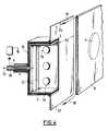
- a vacuum chamber 1which can be evacuated via a suction port 2 to a pressure customary for such plasma processes.
- a hollow anode 3is inserted into the ceiling of the vacuum chamber and is connected to a high-frequency source 6 via an electrically conductive support device 4 and a capacitor 5.
- a second electrode 8which carries a substrate 7 and forms one of the substrate holders.
- the hollow anodehas on its entire (rectangular) circumference a drawn towards the electrode 8 and at the same potential as the hollow anode 3 lying edge 9, which forms a gap "s 1" of 2 mm on all sides with respect to the second electrode.
- the hollow anode 3consequently surrounds a cavity 10, the inner surface 11 of which is enlarged by projections 12 which are formed by parallel ribs (see also FIG. 2). For the distance between these projections, this must be much larger than twice the dark space distance with the applied vacuum, which for vacuums of approx. 2 x 10 ⁇ 2 mbar to a practically usable distance of the projections from each other and from the edge 9 of about 20 mm leads.
- the height of the ribsis not limited here, but it should be in Interest in a good homogeneity of the gas composition in the region of the substrate 7 should not be greater than approximately half the height of the rim 9.
- a gas supply line 13is provided, which is connected to a source (not shown) for the gas to be used.
- the gas feed line 13opens into the cavity 10, and the gas distribution can still be improved by a distributor pipe, not shown here, which extends over a greater part of the length or width of the cavity 10 and has a large number of outlet bores over its entire length.
- the lower circumferential (rectangular) edge of the edge 9, which also defines the gap with the width "s1"is the opening of the hollow anode 3rd
- the hollow anode 3is - with the exception of the lower opening - surrounded on all sides by a rectangular dark room shield 14, the edge 15 of which forms a gap "2" with a width of 2 mm relative to the second electrode 8.
- the entry and exit of the unused reaction products of the supplied gasestakes place via the columns s 1 and s 2.
- the dark room shield 14is via a further support device 16 electrically conductively connected to the vacuum chamber 1 and is consequently at ground potential with the vacuum chamber.
- the vacuum chamber 1is connected to a vacuum lock, not shown here, through which the electrodes 8 serving as substrate holders are sequentially introduced into and out of the system.
- the electrode 8is shown in dashed lines on its way in two further positions 8a and 8b.
- FIG. 3shows two further variants of the projections 12 in FIG. 1, namely that projections are shown in the left half of FIG. 3 that complement one another in a honeycomb pattern, while projections are shown in the right half of FIG. 3 that intersect Hinges of ribs are formed.
- FIG. 4shows a hollow anode 3 cut along its one plane of symmetry with projections 12 and a dark room shield 14 in a complete analogy to FIG. 1.
- an electrical coupling element 17which is in the form of a rectangular, flat frame made of metal and electrically conductive with the darkroom shield 14 is connected.
- the frame width b1 and b2is between about 4 and 12 cm. The arrangement is such that the coupling element 17 is exactly flush with the open underside or edge of the dark room shield 14.
- the substrate 7 carrying the electrode 8is passed at a distance from the gap s2 parallel to the coupling element 7 in the direction of the two arrows 18 past the opening of the hollow anode 3, it being sufficient for the purpose of a completely sufficient electrical coupling of the electrode 8 if this electrode three Circumferential sides of the coupling element 17 covered.
- FIG. 5shows, on an enlarged scale, sections from wall parts, namely from the edges of the hollow anode 3 and the dark room shield 14.
- the aligned openings 19 and 19aare provided with high-frequency-opaque gratings 20 and 20a, in front of which a shielding element 21 is arranged in the form of a circular disk is, facing the cavity 10.
- a shielding element 21is arranged in the form of a circular disk is, facing the cavity 10.
- the shielding element 21serves to prevent the mesh from being atomized during open operation of the hollow anode (without electrode 8 in front of the hollow anode).
- the distance of this shielding element from the assigned surface of the hollow anode 3is approximately 5 mm.
- FIG. 6shows a variant of the object according to FIG. 4, in which the second electrode 22 consists of a metallic cooling roller over which a band-shaped substrate 23 is guided, which comes from a supply roll 24 and is guided to a winding roll 25.
- the remaining rollers in betweenare either guide rollers or cooling rollers for further treatments, which, however, are of no further interest here.
- the dark room shield 14is shown here, which, like the hollow anode (not shown), is adapted to the cylindrical contour of the electrode 22. In order to keep the axial extent of the arrangement low, this is electrical coupling element 17 composed of several parts.
- the coupling element 17has a cylindrical section 17a on each side, of which only the front section can be seen in FIG.
- the coupling element 17consists of two flat sections 17b, of which only the front section is also visible.
- the sections 17a and 17bmeet the requirement that they run at a distance from the gap s2 substantially parallel to the adjacent surface of the second electrode 22.
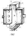
- FIG. 7shows the mirror-symmetrical doubling of the device according to FIG. 4, namely that the hollow anode 3 is arranged opposite a second hollow anode 3 'in such a way that its edges 9 and 9' are aligned with one another and the coupling elements 17 and 17 'have a space 26 between them include, which is used for the passage of appropriately shaped substrates, with or without a special substrate holder. If one is omitted, the substrate takes on the role of the second electrode.
- the required guiding devicesare not shown for the sake of simplicity.
- the coupling elements 17 and 17 'are more or less, but in any case electrically conductive, connected to one another by a frame 27 or 27', a slot 28 being provided in the lower wall of the frame 27 'for the passage of a transport device, not shown.
- the hollow anode 3 'canhave its own high-frequency source or can be connected to the high-frequency source 6 of the hollow anode 3.
- the hollow anodes 3 and 3 'canalso be combined with one another to form an anode box which only has inlet and outlet openings for the substrates or the second electrode.
- the opening of the hollow anode 3had the dimensions 40 cm ⁇ 10 cm.
- An argon atmospherewas maintained at a pressure of 2 x 10 ⁇ 2 mbar, and the hollow anode was operated at a frequency of 13.56 MHz and a total power of 420 watts.
- the second electrode 8was not yet in front of the opening, so that the "hollow anode” was operated as a cathode, which was recognizable by the formation of a clearly visible plasma in the region of the opening. A bias voltage was not measurable. Then the second electrode 8, on which one turned off Metal existing substrate 7 was in front of the cathode.
- the power coupled into the plasmajumped to the previously set target value of 1 kW. This corresponded to an area power of 2.5 W / cm2 on the substrate surface lying under the hollow anode.
- a DC voltage of 1 kVbuilt up between the hollow anode and the substrate, as a result of which the substrate was negatively biased.
- the electrode 8was stopped and the substrate was etched. A subsequent examination of the substrate showed that the etching rate was 1.0 nm / s.
- a pressure of 3 x 10 ⁇ 2 mbar acethylene (C2H2)was maintained dynamically.
- a plasmawas visible in the opening of the hollow anode after the high-frequency source was switched on, and a power of 420 watts was also set without a bias voltage being detectable.
- the power coupled into the plasmajumped to the previously set target value of 1 kW, corresponding to an area power of 2.5 W / cm 2.
- the bias voltage in this casewas 600 V. This process was for the Duration of 100 s continued.
- the subsequent testrevealed a layer of amorphous carbon with a thickness of 300 nm, corresponding to a static coating rate of 3 nm / s.
- the interference color generated by the substrate surface and the layerdid not result in any discernible deviations in the layer thickness in the entire area of the opening of the hollow anode except for a narrow edge area of approximately 5 mm in width.
Landscapes
- Physics & Mathematics (AREA)
- Engineering & Computer Science (AREA)
- Plasma & Fusion (AREA)
- Chemical & Material Sciences (AREA)
- Analytical Chemistry (AREA)
- Chemical Vapour Deposition (AREA)
- Drying Of Semiconductors (AREA)
- Plasma Technology (AREA)
- Treatments Of Macromolecular Shaped Articles (AREA)
- ing And Chemical Polishing (AREA)
Abstract
Description
Translated fromGermanDie Erfindung betrifft eine Vorrichtung zur Plasmabehandlung von Substraten in einer durch Hochfrequenz angeregten Plasmaentladung zwischen zwei durch eine Hochfrequenzquelle versorgten Elektroden, von denen die erste als Hohlanode ausgebildet und die zweite, das Substrat tragende Elektrode, dem Hohlraum der Anode vorgelagert oder an diesem vorbeiführbar ist, wobei die Hohlanode eine in Richtung auf die zweite Elektrode vorgezogene, auf gleichem Potential wie die Hohlanode liegenden Rand aufweist, der gegenüber der zweiten Elektrode allseitig einen Spalt "s₁" von maximal 10 mm Breite bildet.The invention relates to a device for the plasma treatment of substrates in a plasma discharge excited by high frequency between two electrodes supplied by a high frequency source, of which the first is designed as a hollow anode and the second electrode carrying the substrate is arranged in front of the cavity of the anode or can be guided past it. wherein the hollow anode is drawn in the direction of the second electrode, at the same potential as the hollow anode edge, which forms a gap "s 1" of a maximum of 10 mm in width on all sides with respect to the second electrode.
Bei der Plasmabehandlung, für die die Vorrichtung vorgesehen ist, kann es sich um Plasmaätzen, um die Herstellung von Polymerschichten auf den Substraten durch Plasmapolymerisation, um die Aktivierung von Substratoberflächen etc. handeln.The plasma treatment for which the device is intended can be plasma etching, the production of polymer layers on the substrates by plasma polymerization, the activation of substrate surfaces, etc.
Oblicherweise enthalten Vorrichtungen zur Plasmabehandlung von Substraten mittels Hochfrequenz zwei Elektroden, von denen die eine durch die Vakuumkammer und/oder durch den Substrathalter gebildet wird, die beide aus metallischen Werkstoffen bestehen. Es ist bekannt, daß sich dabei jeweils an derjenigen Elektrode eine gegenüber dem Plasma überwiegend negative Spannung ausbildet, die in Bezug auf die als Gegenelektrode wirkenden Oberflächen die kleinere wirksame Oberfläche aufweist. Die negativ vorgespannte Elektrode wird daher auch hier regelmäßig als "Katode" bezeichnet.Devices for the plasma treatment of substrates by means of high frequency usually contain two electrodes, one of which is formed by the vacuum chamber and / or by the substrate holder, both of which are made of metallic materials. It is known that a voltage which is predominantly negative with respect to the plasma and which has the smaller effective surface with respect to the surfaces acting as counterelectrode is formed in each case on that electrode. The negatively biased electrode is therefore also referred to here regularly as the "cathode".
Bei Verwendung eines plattenförmigen Substrathalters, der mit der Vakuumkammer auf gleichem Potential liegt und damit die eine Elektrode bildet, einerseits, und bei Verwendung einer plattenförmigen, dem Substrathalter gegenüberliegenden Elektrode andererseits, bildet sich aufgrund der hierdurch notwendigerweise vorgegebenen Flächenverhältnisse an der zuletzt genannten Elektrode das negative Potential aus. Dadurch wird auf dieser Elektrode (= Katode) befindliches Material (= Target) zerstäubt und auf dem Substrat niedergeschlagen. Will man in einer solchen Vorrichtung ätzen, so müssen Substrate und Target sinngemäß vertauscht werden.When using a plate-shaped substrate holder, which is at the same potential with the vacuum chamber and thus forms the one electrode, on the one hand, and when using a plate-shaped electrode opposite the substrate holder, on the other hand, the resulting area ratios on the last-mentioned electrode result in the negative Potential. As a result, material (= target) located on this electrode (= cathode) is atomized and deposited on the substrate. If you want to etch in such a device, substrates and target must be exchanged accordingly.
Bei Verwendung von Gleichspannung ist die Polarität der Elektroden durch ihre Verbindung mit dem jeweiligen Pol der Gleichspannungsquelle zwingend vorgegeben. Durch die DE-OS 21 15 590 ist es beispielsweise bekannt, eine Hohlkatode mit einem in Richtung auf den Substratträger vorspringenden Rand zu verwenden, um die Gleichmäßigkeit der Schichtdickenverteilung zu verbessern. Dieser vorspringende Rand führt aber bei Verwendung von Gleichspannung nicht zu einer Umkehrung der Polarität.When using DC voltage, the polarity of the electrodes is mandatory due to their connection to the respective pole of the DC voltage source. From DE-OS 21 15 590 it is known, for example, to use a hollow cathode with an edge projecting in the direction of the substrate carrier in order to improve the uniformity of the layer thickness distribution. However, this protruding edge does not lead to a reversal of the polarity when using DC voltage.
Durch die DE-PS 22 41 229 ist eine Vorrichtung gemäß Gattungsbegriff bekannt, bei der durch Verwendung von Hochfrequenz erreicht wird, daß die hohle Elektrode wegen ihres Randes relativ zu der dem Hohlraum unmittelbar zugekehrten Oberfläche der anderen Elektrode (des Substrathalters) die größere Oberfläche aufweist und hierdurch die Funktion einer Anode erhält, so daß also gewissermaßen eine Umkehrung der Verhältnisse bezüglich der Vorspannung erfolgt. Dies läßt sich vereinfacht so erklären, daß der Rand der Hohlanode einen Entladungsraum eingrenzt, relativ zu welchem die außerhalb liegenden metallischen Teile der Vorrichtung keine Elektrodenfunktion mehr ausüben, so daß die Verhältnisse ausschließlich durch die einander zugekehrten Oberflächenteile der Hohlanode einerseits und des Substrathalters andererseits bestimmt werden. Man kann dies ald "Randeffekt" bezeichnen.From DE-PS 22 41 229 a device according to the generic term is known in which the use of high frequency ensures that the hollow electrode has the larger surface because of its edge relative to the surface of the other electrode (the substrate holder) directly facing the cavity and thereby maintains the function of an anode, so that, as it were, there is a reversal of the conditions with regard to the bias voltage. This can be explained in a simplified way that the edge of the hollow anode delimits a discharge space, relative to which the metallic parts of the device lying outside no longer perform an electrode function, so that the conditions are determined exclusively by the facing surface parts of the hollow anode on the one hand and the substrate holder on the other . One can call this "edge effect".
Die bekannte Lösung führt jedoch im Falle einer Anwendung dieses Prinzips bei bestimmten Vorrichtungen mit kontinuierlichem Substrattransport zu einigen Schwierigkeiten: Wird nämlich der Substrathalter mit dem Substrat entfernt, so wirkt als Gegenelektrode mindestens die metallische Grundplatte der Vakuumkammer, die in der Regel eine größere Fläche als die hohle Elektrode besitzt und an Masse gelegt ist. In diesem Fall bildet sich in völliger Umkehrung der Potentialverhältnisse die negative Spannung auf der Hohlelektrode aus, die nunmehr als Katode wirkt.However, the known solution leads to some difficulties when using this principle in certain devices with continuous substrate transport: namely, if the substrate holder with the substrate is removed, at least the metallic base plate of the vacuum chamber, which generally has a larger area than that, acts as the counter electrode has a hollow electrode and is connected to ground. In this case, the negative voltage on the hollow electrode, which now acts as a cathode, forms in a complete reversal of the potential relationships.
Daraus ergibt sich, daß die Größe des Spaltes zwischen dem Rand der Hohlelektrode einerseits und dem Substrat bzw. Substrathalter andererseits von wesentlicher Bedeutung für die Ausbildung der Potentialverteilung im Bereich des vom Plasma erfüllten Raumes ist. Da der erwähnte Spalt die Verbindung des Plasmas zu dessen Umgebung darstellt, entscheidet die Spaltgröße darüber, ob die Hohlelektrode als Anode oder als Katode der Anordnung wirkt. Durch Versuche wurde festgestellt, daß eine Vergrößerung des genannten Spaltes über einen Betrag von etwa 1 mm hinaus den Einfluß der übrigen metallischen Vorrichtungsteile drastisch vergrößert, und zwar mit der Konsequenz der Ausbildung einer negativen Vorspannung auf der Hohlelektrode anstatt auf dem Substrat. Derartige Spaltvergrößerungen sind nun aber bei kontinuierlichen Vorrichtungen, bei denen die Substrate auf beweglichen Substrathaltern angeordnet sind, praktisch unvermeidbar, insbesondere dann, wenn derartige Substrathalter mit Abständen zueinander an der Öffnung der Hohlelektrode vorbeigeführt werden. Auch kann der betreffende Spalt nicht beliebig klein gehalten werden, da dies nicht nur eine außerordentlich präzise Führung der Substrathalter erforderlich macht, sondern weil auch die gegebenenfalls auf der Oberfläche des Substrathalters liegenden Substrate bei ihrem Durchlauf durch die Anlage die Spaltweite verändern, wenn man nicht den sehr aufwendigen Weg geht, für jede Substratform und -größe unterschiedliche Substrathalter einzusetzen, in denen die Substrate vertieft und bündig mit der Oberfläche des Substrathalters angeordnet sind. Damit wird die Anwendungsbreite des bekannten Prinzips stark eingeschränkt.It follows from this that the size of the gap between the edge of the hollow electrode on the one hand and the substrate or substrate holder on the other hand is of essential importance for the formation of the potential distribution in the area of the space filled by the plasma. Since the gap mentioned represents the connection of the plasma to its surroundings, the gap size decides whether the hollow electrode acts as an anode or as a cathode of the arrangement. Experiments have shown that increasing the gap above an amount of about 1 mm dramatically increases the influence of the other metallic parts of the device, with the consequence of the formation of a negative bias on the hollow electrode instead of on the substrate. Such enlargements of the gap are now continuous Devices in which the substrates are arranged on movable substrate holders are practically unavoidable, in particular when such substrate holders are guided past the opening of the hollow electrode at intervals from one another. Also, the gap in question cannot be kept arbitrarily small, since this not only requires an extremely precise guidance of the substrate holder, but also because the substrates, which may lie on the surface of the substrate holder, change the gap width as they pass through the system, if one does not very expensive way is to use different substrate holders for each substrate shape and size, in which the substrates are recessed and arranged flush with the surface of the substrate holder. This severely limits the scope of the known principle.
Der Erfindung liegt daher die Aufgabe zugrunde, eine Vorrichtung der eingangs beschriebenen Gattung dahingehend zu verbessern, daß sie unempfindlicher gegen eine Vergrößerung des Spaltes ist und insbesondere auch in Vorrichtungen mit kontinuierlichem oder quasikontinuierlichem Substrattransport eingesetzt werden kann, d.h. in sogenannten "In-Line-Anlagen".The invention is therefore based on the object of improving a device of the type described at the outset in such a way that it is less sensitive to an increase in the gap and in particular can also be used in devices with continuous or quasi-continuous substrate transport, i.e. in so-called "in-line systems".
Die Lösung der gestellten Aufgabe erfolgt bei der eingangs angegebenen Vorrichtung erfindungsgemäß dadurch, daß im Hohlraum der Hohlanode an deren innerer Oberfläche oberflächenvergrößernde Vorsprünge angeordnet sind.The object is achieved in the device specified at the outset according to the invention in that in the cavity of the hollow anode on its interior Surface enlarging projections are arranged.
Durch diese Vorsprünge wird die dem Plasma zugekehrte Oberfläche der Hohlanode erheblich vergrößert, so daß der Plasmaeinschuß auch bei einer merklichen Vergrößerung der Spaltweite erhalten bleibt und auch dann noch keine Umkehrung der Potentialverhältnisse erfolgt, wenn fahrbare oder verschiebbare Substrathalter relativ zur Öffnung der Hohlanode transportiert werden. Die geometrische Form der Vorsprünge ist dabei nicht kritisch; sie sollen lediglich eine möglichst große Oberflächenvergrößerung bewirken, wobei allerdings die Abstände der Vorsprünge untereinander bzw. die zwischen den Vorsprüngen und dem Rand gebildeten Hohlräume nicht so klein dimensioniert werden dürfen, daß die Oberflächenvergrößerung in Bezug auf das Plasma unwirksam würde. Die Abstände dürfen also das zweifache Maß des sogenannten "Dunkelraumabstandes" nicht unterschreiten. Weiterhin hat die Vergrößerung der inneren Oberfläche der Hohlanode eine Vergrößerung der sich auf der Oberfläche des Substrats bzw. des Substrathalters, relativ zur Hohlanode ausbildenden negativen Spannung zur Folge. Hieraus resultiert eine entsprechende Erhöhung der kinetischen Energie der aus dem Plasmaraum auf das Substrat auftreffenden, positiv geladenen Ionen.By means of these projections, the surface of the hollow anode facing the plasma is considerably enlarged, so that the plasma weft is retained even with a noticeable increase in the gap width and there is still no reversal of the potential relationships when mobile or displaceable substrate holders are transported relative to the opening of the hollow anode. The geometric shape of the protrusions is not critical; they should only bring about the greatest possible surface enlargement, although the spacing of the projections from one another or the cavities formed between the projections and the edge must not be dimensioned so small that the surface enlargement would be ineffective with respect to the plasma. The distances must therefore not be less than twice the so-called "dark room distance". Furthermore, the increase in the inner surface of the hollow anode results in an increase in the negative voltage which forms on the surface of the substrate or the substrate holder relative to the hollow anode. This results in a corresponding increase in the kinetic energy of the positively charged ions striking the substrate from the plasma space.
Dies führt für den Fall der Verwendung der erfindungsgemäßen Vorrichtung als Ätz vorrichtung in einer Erhöhung der spezifischen Ätzrate. Für den Fall der Abscheidung von Schichten aus der Gasphase führt der Beschuß der auf dem Substrat aufwachsenden Schicht mit positiven Ionen wegen des gleichzeitigen Absputterns der schwächer gebundenen Teilchen der Schicht zu besonders hochwertigen Schichten.If the device according to the invention is used as an etching device, this leads to an increase in the specific etching rate. In the case of the deposition of layers from the gas phase, the bombardment of the layer growing on the substrate with positive ions leads to particularly high-quality layers because of the simultaneous sputtering off of the weakly bound particles of the layer.
Durch die erfindungsgemäße Maßnahme bleiben die Eigenschaften der Hohlanode auch bei einem laufenden Substrattransport voll erhalten: Das Plasma ist durch materielle Wände vollständig eingeschlossen, im Gegensatz beispielsweise zu einem Einschluß durch Magnetfelder, der insbesondere bei Anwendung von Hochfrequenz nie vollständig ist. Weiterhin wird durch den vollständigen Einschluß durch die Hohlanode im Plasmaraum eine Plasmadichte erreicht, die bei einem Plasmaeinschluß mittels magnetischer Felder nicht erreichbar ist, vergleichbare elektrische Leistungen pro Flächeneinheit vorausgesetzt. Darüberhinaus haben Untersuchungen gezeigt, daß die Plasmadichte im gesamten Hohlraum der Hohlanode mit Ausnahme einer Abnahme im unmittelbaren Randbereich so gleichmäßig ist, daß eine Abweichung optisch nicht beobachtet werden kann. Der Abfall der Plasmadichte im Randbereich beschränkt sich auf weniger als 5 mm. Dies führt zu Schichtdickenabweichungen, die kleiner als ± 3 % sind, ein Wert, der mit einem magnetischen Einschluß des Plasmas nicht erreicht werden kann.As a result of the measure according to the invention, the properties of the hollow anode are fully retained even when the substrate is being transported: the plasma is completely enclosed by material walls, in contrast to, for example, an inclusion by magnetic fields, which is never complete, especially when high frequency is used. Furthermore, through the complete containment by the hollow anode reached a plasma density in the plasma space that cannot be achieved with plasma confinement by means of magnetic fields, provided comparable electrical powers per unit area. In addition, studies have shown that the plasma density in the entire hollow space of the hollow anode, with the exception of a decrease in the immediate edge area, is so uniform that a deviation cannot be observed optically. The drop in plasma density in the edge area is limited to less than 5 mm. This leads to deviations in the layer thickness which are smaller than ± 3%, a value which cannot be achieved with magnetic confinement of the plasma.
Die erfindungsgemäße Ausbildung der Anode ist dabei leicht durchzuführen, und zwar durch ein Gießverfahren oder durch Zusammensetzung aus metallischem Streifenmaterial. Auch kann die erfindungsgemäße Hohlanode leicht gegen eine solche nach dem Stand der Technik ausgetauscht werden, ohne daß es umständlicher Umbauten an der gesamten Vorrichtung bedarf.The formation of the anode according to the invention is easy to carry out, namely by a casting process or by a composition of metallic strip material. The hollow anode according to the invention can also be easily exchanged for one according to the prior art without the need for laborious modifications to the entire device.
Die erfindungsgemäße Vorrichtung eignet sich für die Plasmapolymerisation, d.h. für die Abscheidung von Polymerisatschichten auf den Substraten, insbesondere aber für die Abscheidung von amorphem Kohlenstoff als Schutzschicht auf Substraten. Für die zuletzt genannten Zwecke wird ein gasförmiger Kohlenwasserstoff in den Hohlraum der Hohlanode eingeleitet, wobei die Abfuhr der Reaktionsprodukte (hauptsächlich Wasserstoff) auf weiter unten noch näher beschriebenen Wegen geschieht.The device according to the invention is suitable for plasma polymerization, ie for the deposition of polymer layers on the substrates, but in particular for the deposition of amorphous carbon as a protective layer on substrates. For the latter For this purpose, a gaseous hydrocarbon is introduced into the cavity of the hollow anode, the reaction products (mainly hydrogen) being removed in ways described in more detail below.
Bei Hohlanoden, die in eine Vakuumkammer derart hineinragen, daß auch ihre Außenseiten mindestens teilweise dem Vakuum ausgesetzt sind, ist es erforderlich, daß die Hohlanode auf ihrer Außenseite allseitig von einer Dunkelraumabschirmung umgeben ist, die gleichfalls einen in Richtung auf die zweite Elektrode vorgezogenen, auf gleichem Potential wie die Dunkelraumabschirmung liegenden Rand aufweist. Dabei ist es in weiterer Ausgestaltung der Erfindung besonders vorteilhaft, wenn der Rand der Dunkelraumabschirmung gegenüber der zweiten Elektrode (dem Substrathalter) allseitig einen Spalt "s₂" von maximal 10 mm bildet.In the case of hollow anodes which protrude into a vacuum chamber in such a way that their outer sides are also at least partially exposed to the vacuum, it is necessary that the outer side of the hollow anode is surrounded on all sides by a dark room shield, which is likewise pulled forward towards the second electrode has the same potential as the edge of the dark room shield. In a further embodiment of the invention, it is particularly advantageous if the edge of the dark room shield forms a gap "s₂" of a maximum of 10 mm on all sides with respect to the second electrode (the substrate holder).
Eine derartige Vorrichtung kann gemäß der wiederum weiteren Ausgestaltung der Erfindung zusätzlich dadurch gekennzeichnet sein, daß auf mindestens einem Teil des Umfangs der Dunkelraumabschirmung elektrische Koppelelemente angeordnet sind, die im Abstand des Spaltes "s₂" im wesentlichen parallel zur benachbarten Oberfläche der zweiten Elektrode verlaufen. Derartige Koppelelemente bringen den zusätzlichen Vorteil mit sich, daß der Spalt "s₁" noch größer dimensioniert werden kann bevor der "Randeffekt" verschwindet.Such a device can, according to the yet further embodiment of the invention, be additionally characterized in that electrical coupling elements are arranged on at least part of the circumference of the dark room shielding, which run essentially parallel to the adjacent surface of the second electrode at a distance from the gap "s₂". Coupling elements of this type have the additional advantage that the gap "s 1" can be dimensioned even larger before the "edge effect" disappears.
Beispiele und Möglichkeiten zur geometrischen Ausbildung dieser Koppelelemente sind in der Detailbeschreibung näher erläutert. Zur Erläuterung ihrer Bedeutung sei nochmals auf den Stand der Technik nach der DE-PS 22 41 299 hingewiesen.Examples and possibilities for the geometric design of these coupling elements are explained in more detail in the detailed description. To explain their meaning, reference is again made to the prior art according to DE-PS 22 41 299.
Trotz direkter Verbindung des Substrathalters mit dem Hochfrequenz-Massepunkt, d.h. mit der metallischen Vakuumkammer, durch eine beidseitig verschraubte Kupferlitze großen Querschnitts lag der Substrathalter keineswegs auf Massepotential, was an der Ausbildung einer geschlossenen Plasmazone um den gesamten Substrathalter erkennbar war. Die Verhältnisse sind bei Anlagen mit beweglichen Substrathaltern noch weitaus schwieriger zu beherrschen, da dort eine Masseverbindung durch feste Anschlüsse ohnehin nicht herzustellen ist.Despite the direct connection of the substrate holder to the high-frequency ground point, i.e. with the metallic vacuum chamber, through a copper wire with a large cross-section screwed on both sides, the substrate holder was by no means at ground potential, which was evident from the formation of a closed plasma zone around the entire substrate holder. The conditions are much more difficult to control in systems with movable substrate holders, since there is no connection to earth with fixed connections anyway.
Durch die erfindungsgemäße Anordnung von Koppelelementen, die vorzugsweise aus Blechen bestehen, die parallel zur benachbarten Oberfläche des Substrathalters verlaufen, wird unter Hochfrequenzbedingungen eine Ankopplung des Substrathalters an die Dunkelraumabschirmung erreicht, wodurch der Einschluß des Plasmas noch weiter verbessert wird. Bei genügender Länge bzw. Breite der Koppelelemente von beispielsweise 10 cm, konnte sogar bei einem ansonsten isoliert aufgestellten Substrathalter ein einwandfreier Einschluß des Plasmas mit einer negativen Vorspannung am Substrathalter erreicht werden, und zwar für Abstände s₂ bis zu 3 mm.Due to the arrangement of coupling elements according to the invention, which preferably consist of sheets that run parallel to the adjacent surface of the substrate holder, coupling of the substrate holder to the dark room shield is achieved under high-frequency conditions, whereby the inclusion of the plasma is further improved. With sufficient length or width of the coupling elements of, for example, 10 cm, even with an otherwise isolated substrate holder, it was possible to properly enclose the plasma with a negative bias on the substrate holder, for distances s₂ of up to 3 mm.
Der Einschluß des Plasmas und die volle negative Vorspannung des Substrathalters blieben bei verfahrbaren Substrathaltern selbst dann erhalten, wenn die eine Kante des Substrathalters den Hohlraum der Hohlanode gerade eben abdeckte. Bei einer Oberflächengröße der Koppelelemente von 800 cm² und einem Abstand s₂ von 0,3 cm wird beispielhaft ein Plattenkondensator mit einer Kapazität von 235 pF gebildet, woraus sich für die übliche Frequenz von 13,56 MHz ein Wechselstromwiderstand von R = 313 Ohm errechnet. Bei den üblichen Bias-Spannungen von 1 kV können somit über diese Kapazität ohne weiteres Leistungen in der Größenordnung von 1 bis 2 kW übertragen werden. Erst ab einer Leistung von etwa 1,5 kW (entsprechend einer Flächenleistung von ca. 4 W/cm² Substratfläche konnte eine, allerdings extrem schwache, Plasmaausbildung um den Substrathalter beobachtet werden, was jedoch keine erkennbaren Auswirkungen auf die Polaritäts-Verhältnisse im Plasmaraum hatte, d.h. die über die Koppelelemente bewirkte rein kapazitive Ankopplung des Substrathalters an den Hochfrequenz-Nullpunkt war wesentlich wirksamer als die beim Stand der Technik übliche Verbindung über eine Kupferlitze. Dabei ist ein Spalt s₂ in der Größenordnung von 3 mm ohne weiteres auch für sehr große Substrathalter realisierbar.The inclusion of the plasma and the full negative bias of the substrate holder remained with movable Obtain substrate holders even if one edge of the substrate holder just just covered the cavity of the hollow anode. With a surface size of the coupling elements of 800 cm² and a distance s₂ of 0.3 cm, a plate capacitor with a capacitance of 235 pF is formed as an example, from which an AC resistance of R = 313 ohms is calculated for the usual frequency of 13.56 MHz. With the usual bias voltages of 1 kV, capacities in the order of magnitude of 1 to 2 kW can thus be transmitted without any additional effort. Only from a power of about 1.5 kW (corresponding to an area power of approx. 4 W / cm² substrate area could an, however extremely weak, plasma formation be observed around the substrate holder, which, however, had no discernible effects on the polarity conditions in the plasma space, That is, the purely capacitive coupling of the substrate holder to the high-frequency zero point, which was brought about via the coupling elements, was considerably more effective than the connection via a copper wire which is customary in the prior art .
Weitere vorteilhafte Ausgestaltungen des Erfindungsgegenstandes sind in den übrigen Unteransprüchen angegeben bzw. in der nachstehenden Detailbeschreibung näher erläutert.Further advantageous refinements of the subject matter of the invention are specified in the remaining subclaims or are explained in more detail in the detailed description below.
Es zeigen:
- Figur 1
- einen vertikalen Axialschnitt durch eine vollständige Vorrichtung für den Durchlauf plattenförmiger Substrathalter,
Figur 2- eine Unteransicht der Hohlanode aus der Ebene II-II in Figur 1m
Figur 3- eine Unteransicht
analog Figur 2, jedoch mit zweifach verschiedener Ausbildung der Vorsprünge innerhalb der Hohlanode, - Figur 4
- eine perspektivische Darstellung einer Hohlanode mit einem Koppelelement, aufgeschnitten entlang einer Symmetrieebene der Hohlanode,
Figur 5- ein Detail aus Figur 4 in perspektivischer Darstellung in vergrößertem Maßstab,
Figur 6- eine Anordnung analog Figur 4 jedoch mit einem walzenförmigen Substrathalter für die Plasmabehandlung von flexiblen, bandförmigen Substraten und
Figur 7- eine Verdoppelung der Vorrichtung nach Figur 4 in spiegelsymmetrischer Anordnung.
- Figure 1
- a vertical axial section through a complete device for the passage of plate-shaped substrate holder,
- Figure 2
- a bottom view of the hollow anode from the plane II-II in Figure 1m
- Figure 3
- 3 shows a bottom view analogous to FIG. 2, but with two different designs of the projections within the hollow anode,
- Figure 4
- 2 shows a perspective illustration of a hollow anode with a coupling element, cut open along a plane of symmetry of the hollow anode,
- Figure 5
- 4 shows a detail from FIG. 4 in a perspective illustration on an enlarged scale,
- Figure 6
- an arrangement analogous to Figure 4 but with a roller-shaped substrate holder for the plasma treatment of flexible, ribbon-shaped substrates and
- Figure 7
- a doubling of the device according to Figure 4 in a mirror-symmetrical arrangement.
In Figur 1 ist eine Vakuumkammer 1 dargestellt, die über einen Saugstutzen 2 auf einen für derartige Plasmaprozesse üblichen Druck evakuierbar ist. In die Decke der Vakuumkammer ist eine Hohlanode 3 eingesetzt, die über eine elektrisch leitende Tragvorrichtung 4 und einen Kondensator 5 mit einer Hochfrequenzquelle 6 verbunden ist. Unterhalb der Hohlanode 3 befindet sich eine zweite, ein Substrat 7 tragende Elektrode 8, die einen der Substrathalter bildet. Die Hohlanode besitzt auf ihrem gesamten (rechteckigen) Umfang einen in Richtung auf die Elektrode 8 vorgezogenen und auf gleichem Potential wie die Hohlanode 3 liegenden Rand 9, der gegenüber der zweiten Elektrode allseitig einen Spalt "s₁" von 2 mm bildet.In Figure 1, a vacuum chamber 1 is shown, which can be evacuated via a
Die Hohlanode 3 umschließt infolgedessen einen Hohlraum 10, dessen innere Oberfläche 11 durch Vorsprünge 12 vergrößert ist, die durch parallele Rippen gebildet werden (siehe auch Figur 2). Für den Abstand dieser Vorsprünge gilt, daß dieser wesentlich größer sein muß, als der zweifache Dunkelraumabstand bei dem angewandten Vakuum, was bei Vakua von ca. 2 x 10⁻² mbar zu einem praktisch brauchbaren Abstand der Vorsprünge voneinander und vom Rand 9 von etwa 20 mm führt. Die Höhe der Rippen ist hierbei nicht beschränkt, sie sollte jedoch im Interesse einer guten Homogenität der Gaszusammensetzung im Bereich des Substrats 7 nicht größer sein, als etwa die Hälfte der Höhe des Randes 9. Diese Verhältnisse sind in Figur 1 etwa maßstäblich dargestellt.The
Für die Einführung entsprechender Behandlungsgase ist eine Gas-Zuleitung 13 vorgesehen, die mit einer nicht dargestellten Quelle für das einzusetzende Gas verbunden ist. Die Gaszuleitung 13 mündet in den Hohlraum 10, wobei die Gasverteilung noch durch ein hier nicht gezeigtes Verteilerrohr verbessert werden kann, das sich über einen größeren Teil der Länge oder Breite des Hohlraums 10 erstreckt und auf seiner gesamten Länge eine Vielzahl von Austrittsbohrungen aufweist. Die untere umlaufende (rechteckige) Kante des Randes 9, die gleichzeitig den Spalt mit der Weite "s₁" definiert, ist die Öffnung der Hohlanode 3.For the introduction of appropriate treatment gases, a
Die Hohlanode 3 ist - mit Ausnahme der unteren Öffnung - allseitig von einer quaderförmigen Dunkelraumabschirmung 14 umgeben, deren Rand 15 gegenüber der zweiten Elektrode 8 einen Spalt "s₂" mit einer Breite von 2 mm bildet. Der Ein- und Austritt der nicht verbrauchten Reaktionsprodukte der zugeführten Gase erfolgt über die Spalte s₁ und s₂. Die Dunkelraumabschirmung 14 ist über eine weitere Tragvorrichtung 16 mit der Vakuumkammer 1 elektrisch leitend verbunden und liegt infolgedessen mit der Vakuumkammer auf Massepotential.The
Am jeweils linken und rechten Ende ist die Vakuumkammer 1 mit je einer hier nicht dargestellten Vakuumschleuse verbunden, durch die die als Substrathalter dienenden Elektroden 8 sequentiell in die Anlage eingeführt und aus dieser wieder herausgeführt werden. Die Elektrode 8 ist auf ihrem Wege in zwei weiteren Positionen 8a und 8b gestrichelt dargestellt.At the left and right ends in each case, the vacuum chamber 1 is connected to a vacuum lock, not shown here, through which the
Die Figur 3 zeigt zwei weitere Varianten der Vorsprünge 12 in Figur 1, und zwar sind in der linken Hälfte von Figur 3 Vorsprünge dargestellt, die sich zu einem Wabenmuster ergänzen, während in der rechten Hälfte von Figur 3 Vorsprünge dargestellt sind, die als sich kreuzende Scharen von Rippen ausgebildet sind.FIG. 3 shows two further variants of the
Figur 4 zeigt eine entlang ihrer einen Symmetrieebene aufgeschnittene Hohlanode 3 mit Vorsprüngen 12 und einer Dunkelraumabschirmung 14 in völliger Analogie zu Figur 1. Auf dem Umfang der Dunkelraumabschirmung 14, die gleichfalls entlang ihrer einen Symmetrieebene aufgeschnitten dargestellt ist, befindet sich ein elektrisches Koppelelement 17, das in Form eines rechteckigen, ebenen Rahmens ausgebildet ist, der aus Metall besteht und elektrisch leitend mit der Dunkelraumabschirmung 14 verbunden ist. Die Rahmenbreite b₁ und b₂ liegt dabei zwischen etwa 4 und 12 cm. Die Anordnung ist dabei so getroffen, daß das Koppelelement 17 exakt bündig mit der offenen Unterseite bzw. Kante der Dunkelraumabschirmung 14 abschließt. Die das Substrat 7 tragende Elektrode 8 wird im Abstand des Spaltes s₂ parallel zum Koppelelement 7 in Richtung der beiden Pfeile 18 an der Öffnung der Hohlanode 3 vorbeigeführt, wobei es zum Zwecke einer völlig ausreichenden elektrischen Ankopplung der Elektrode 8 bereits genügt, wenn diese Elektrode drei Umfangsseiten des Koppelelements 17 überdeckt.FIG. 4 shows a
Wie aus Figur 4 ferner hervorgeht, befinden sich in den Wandflächen der Hohlanode 3 und der Dunkelraumabschirmung 14 Öffnungen 19 für den Austritt der nicht verbrauchten Reaktionsprodukte der zugeführten Gase. Einzelheiten dieser Öffnungen 19 werden anhand von Figur 5 nunmehr näher erläutert.As can also be seen from FIG. 4, there are
Figur 5 zeigt in vergrößertem Maßstab Ausschnitte aus Wandungsteilen, nämlich aus den Rändern der Hohlanode 3 und der Dunkelraumabschirmung 14. Die miteinander fluchtenden Öffnungen 19 und 19a sind durch hochfrequenzundurchlässige Gitter 20 bzw. 20a versehen, vor denen jeweils ein Abschirmelement 21 in Form einer Kreisscheibe angeordnet ist, und zwar dem Hohlraum 10 zugekehrt. Dadurch wird das Plasma in gleicher Weise wie durch eine feste Wand eingeschlossen, wobei jedoch der Gastransport praktisch nicht behindert wird. Für die vorzugsweise zu verwendende Frequenz von 13,56 MHz kommen hierfür handelsübliche Metallnetze mit einer lichten Weite zwischen den Maschen von einigen Zehntel Millimetern in Frage. Der optische Transmissionsgrad solcher Netze beträgt zwischen 40 und 70 %. Das Abschirmelement 21 dient dazu, das Zerstäuben der Gitter beim offenen Betrieb der Hohlanode (ohne Elektrode 8 vor der Hohlanode) zu verhindern. Der Abstand dieses Abschirmelements von der zugeordneten Oberfläche der Hohlanode 3 beträgt etwa 5 mm.FIG. 5 shows, on an enlarged scale, sections from wall parts, namely from the edges of the
Figur 6 zeigt eine Variante des Gegenstandes nach Figur 4, bei der die zweite Elektrode 22 aus einer metallischen Kühlwalze besteht, über die ein bandförmiges Substrat 23 geführt wird, das von einer Vorratsrolle 24 kommt und zu einer Aufwickelrolle 25 geführt wird. Die übrigen, dazwischenliegenden Walzen sind entweder Führungswalzen oder Kühlwalzen für weitere Behandlungen, die jedoch hier nicht weiter interessieren. Von der Hohlanode ist hier nur die Dunkelraumabschirmung 14 dargestellt, die ebenso wie die nicht gezeigte Hohlanode der zylindrischen Kontur der Elektrode 22 angepaßt ist. Um hierbei die axiale Ausdehnung der Anordnung gering zu halten, ist das elektrische Koppelelement 17 aus mehreren Teilen zusammengesetzt. Im Bereich der Zylinderfläche der Elektrode 22 besitzt das Koppelelement 17 auf jeder Seite ein zylindrisches Teilstück 17a, von dem in Figur 6 nur das vordere zu sehen ist. Im Bereich der kreisförmigen Stirnflächen der zweiten Elektrode 22 besteht das Koppelelement 17 aus zwei ebenen Teilstücken 17b, von denen ebenfalls nur das vordere sichtbar ist. Die Teilstücke 17a und 17b genügen jedoch sämtlich der Forderung, daß sie im Abstand des Spaltes s₂ im wesentlichen parallel zur benachtbarten Oberfläche der zweiten Elektrode 22 verlaufen.FIG. 6 shows a variant of the object according to FIG. 4, in which the
Figur 7 zeigt die spiegelsymmetrische Verdoppelung der Vorrichtung nach Figur 4, und zwar ist der Hohlanode 3 gegenüber eine zweite Hohlanode 3' derart angeordnet, daß ihre Ränder 9 bzw. 9' miteinander fluchten und die Koppelelemente 17 bzw. 17' einen Zwischenraum 26 zwischen sich einschliessen, der zum Hindurchführen entsprechend geformter Substrate dient und zwar mit oder ohne einen besonderen Substrathalter. Bei Verzicht auf einen solchen übernimmt das Substrat die Rolle der zweiten Elektrode. Die erforderlichen Führungseinrichtungen sind der Einfachheit halber nicht dargestellt. Die Koppelelemente 17 und 17' sind durch eine Zarge 27 bzw. 27' mehr oder weniger, jedenfalls aber elektrisch leitend, miteinander verbunden, wobei in der unteren Wand der Zarge 27' ein Schlitz 28 für den Durchgriff einer nicht gezeigten Transporteinrichtung vorhanden ist.FIG. 7 shows the mirror-symmetrical doubling of the device according to FIG. 4, namely that the
In den nicht sichtbaren, vorderen und hinteren Wänden der Zarge 27 bzw. 27' befinden sich übliche Öffnungen. Die Hohlanode 3' kann eine eigene Hochfrequenzquelle aufweisen, oder an die Hochfrequenzquelle 6 der Hohlanode 3 angeschlossen sein. Auch können die Hohlanoden 3 und 3' zu einem Anodenkasten miteinander vereinigt sein, der lediglich Ein- und Austrittsöffnungen für die Substrate bzw. die zweite Elektrode aufweist.There are usual openings in the invisible, front and rear walls of the
Bei einer Vorrichtung nach Figur 4 besaß die Öffnung der Hohlanode 3 die Abmessungen 40 cm x 10 cm. Eine Argonatmosphäre wurde bei einem Druck von 2 x 10⁻² mbar aufrechterhalten, und die Hohlanode wurde mit einer Frequenz von 13,56 MHz und einer Leistung von insgesamt 420 Watt betrieben. Die zweite Elektrode 8 befand sich zu diesem Zeitpunkt noch nicht vor der Öffnung, so daß die "Hohlanode" als Katode betrieben wurde, was an der Ausbildung eines deutlich sichtbaren Plasmas im Bereich der Öffnung erkennbar war. Eine Biasspannung war nicht meßbar. Danach wurde die zweite Elektrode 8, auf der sich ein aus Metall bestehendes Substrat 7 befand, vor die Katode gefahren. In dem Augenblick, in dem die Hohlanode 3 gerade eben von der Elektrode 8 abgedeckt wurde, sprang die in das Plasma eingekoppelte Leistung auf den vorher eingestellten Sollwert von 1 kW. Dies entsprach einer Flächenleistung auf der unter der Hohlanode liegenden Substratfläche von 2,5 W/cm². Gleichzeitig baute sich eine Gleichspannung von 1 kV zwischen der Hohlanode und dem Substrat auf, wodurch das Substrat negativ vorgespannt wurde. In dieser Position wurde die Elektrode 8 angehalten und das Substrat geätzt. Eine anschliessende Untersuchung des Substrats ergab, daß die Ätzrate 1,0 nm/s betrug.In the case of a device according to FIG. 4, the opening of the
In der gleichen Vorrichtung wurde dynamisch ein Druck von 3 x 10⁻² mbar Acethylen (C₂H₂) aufrechterhalten. In analoger Weise wie in Beispiel 1 war in der Öffnung der Hohlanode nach dem Einschalten der Hochfrequenz-Quelle ein Plasma sichtbar, und es wurde eine Leistung von gleichfalls 420 Watt eingestellt, ohne daß eine Bias-Spannung feststellbar war. Nach dem Vorfahren der Elektrode 8 vor die Hohlanode sprang die in das Plasma eingekoppelte Leistung auf den zuvor eingestellten Soll-Wert von 1 kW , entsprechend einer Flächenleistung von gleichfalls 2,5 W/cm². Die Biasspannung betrug in diesem Falle 600 V. Dieser Vorgang wurde für die Dauer von 100 s fortgesetzt. Die anschliessende Prüfung ergab eine Schicht aus amorphem Kohlenstoff mit einer Dicke von 300 nm, entsprechend einer statischen Beschichtungsrate von 3 nm/s. Die von der Substratoberfläche und der Schicht erzeugte Interferenzfarbe ergab im gesamten Bereich der Öffnung der Hohlanode bis auf einen schmalen Randbereich von ca. 5 mm Breite keine erkennbaren Abweichungen hinsichtlich der Schichtdicke.In the same device, a pressure of 3 x 10⁻² mbar acethylene (C₂H₂) was maintained dynamically. In a manner analogous to that in Example 1, a plasma was visible in the opening of the hollow anode after the high-frequency source was switched on, and a power of 420 watts was also set without a bias voltage being detectable. After moving the
Claims (11)
- Device for the plasma processing of substrates in a high-frequency-excited plasma discharge between two electrodes supplied by a high frequency source, the first electrode being formed as a hollow anode and the second electrode, which carries the substrate, being mounted in front of the cavity of the hollow anode or being capable of being guided past the latter, the hollow anode having an edge, which is drawn forward in the direction of the second electrode and which has the same potential as the hollow anode, this edge forming a gap "s₁" of 10 mm maximum width all round with respect to the second electrode, characterised in that surface area-increasing projections (12) are located in the cavity (10) of the hollow anode (3) around its inner surface (11).
- Device according to claim 1, characterised in that the projections (12) are formed as fins projecting from the inner surface (11).
- Device according to claim 2, characterised in that two intersecting groups of fins are provided.
- Device according to claim 1, characterised in that the hollow anode (3) is surrounded all round its exterior by a dark space screen (14), which also has an edge (15) drawn forward in the direction of the second electrode and having the same potential as the dark space screen, this edge forming a gap "s₂" of 10 mm maximum all round with respect to the second electrode (8).
- Device according to claim 4, characterised in that at least one electric coupling element (17, 17a, 17b) is mounted on at least one part of the circumference of the dark space screen (4) and extends at the distance of the gap "s₂" substantially parallel to the adjacent surface of the second electrode (8, 22).
- Device according to claim 1, characterised in that at least one gas supply line (13) leads into the cavity (10).
- Device according to claim 6, characterised in that apertures (19, 19a) for the passage of gas are provided in the wall faces of the hollow anode (3) and of the dark space screen (14), in which apertures grids (20, 20a) are located which transmit high frequencies.
- Device according to claim 7, characterised in that screening elements (21) are associated with the grids (20, 20a) which transmit high frequencies.
- Device according to claim 1, characterised in that for the simultaneous processing of substrates on both sides, two hollow anodes (3, 3') are provided in a mirror-symmetrical arrangement, and make up a substantially closed chamber, and in that the second electrode (8) or the substrate (7) forming the second electrode can be passed between the hollow anodes (3, 3') in the plane of symmetry.
- Device according to claim 9, characterised in that on either side of the plane of symmetry coupling elements (17, 17') are provided parallel to one another and to the second electrode (8) or to the substrate (7) forming the second electrode.
- Application of the device according to claim 1 in connection with the supply of reactive gases for producing on the substrates layers deposited from the gas phase.
Priority Applications (1)
| Application Number | Priority Date | Filing Date | Title |
|---|---|---|---|
| AT87102866TATE73961T1 (en) | 1986-03-04 | 1987-02-27 | DEVICE FOR THE PLASMA TREATMENT OF SUBSTRATES IN A PLASMA DISCHARGE EXCITED BY HIGH FREQUENCY. |
Applications Claiming Priority (2)
| Application Number | Priority Date | Filing Date | Title |
|---|---|---|---|
| DE19863606959DE3606959A1 (en) | 1986-03-04 | 1986-03-04 | DEVICE FOR PLASMA TREATMENT OF SUBSTRATES IN A PLASMA DISCHARGE EXCITED BY HIGH FREQUENCY |
| DE3606959 | 1986-03-04 |
Publications (3)
| Publication Number | Publication Date |
|---|---|
| EP0235770A2 EP0235770A2 (en) | 1987-09-09 |
| EP0235770A3 EP0235770A3 (en) | 1989-09-06 |
| EP0235770B1true EP0235770B1 (en) | 1992-03-18 |
Family
ID=6295415
Family Applications (1)
| Application Number | Title | Priority Date | Filing Date |
|---|---|---|---|
| EP87102866AExpired - LifetimeEP0235770B1 (en) | 1986-03-04 | 1987-02-27 | Device for the plasma processing of substrates in a high frequency excited plasma discharge |
Country Status (6)
| Country | Link |
|---|---|
| US (1) | US4767641A (en) |
| EP (1) | EP0235770B1 (en) |
| JP (1) | JPS62282434A (en) |
| AT (1) | ATE73961T1 (en) |
| DE (2) | DE3606959A1 (en) |
| ES (1) | ES2030006T3 (en) |
Families Citing this family (107)
| Publication number | Priority date | Publication date | Assignee | Title |
|---|---|---|---|---|
| US6784033B1 (en) | 1984-02-15 | 2004-08-31 | Semiconductor Energy Laboratory Co., Ltd. | Method for the manufacture of an insulated gate field effect semiconductor device |
| US6786997B1 (en) | 1984-11-26 | 2004-09-07 | Semiconductor Energy Laboratory Co., Ltd. | Plasma processing apparatus |
| JPH0752718B2 (en)* | 1984-11-26 | 1995-06-05 | 株式会社半導体エネルギー研究所 | Thin film formation method |
| US6113701A (en) | 1985-02-14 | 2000-09-05 | Semiconductor Energy Laboratory Co., Ltd. | Semiconductor device, manufacturing method, and system |
| US6673722B1 (en) | 1985-10-14 | 2004-01-06 | Semiconductor Energy Laboratory Co., Ltd. | Microwave enhanced CVD system under magnetic field |
| US6230650B1 (en) | 1985-10-14 | 2001-05-15 | Semiconductor Energy Laboratory Co., Ltd. | Microwave enhanced CVD system under magnetic field |
| DE3612721C3 (en)* | 1986-04-16 | 1994-07-14 | Ver Glaswerke Gmbh | Continuous sputtering system |
| JPS6393881A (en)* | 1986-10-08 | 1988-04-25 | Anelva Corp | plasma processing equipment |
| US5755886A (en)* | 1986-12-19 | 1998-05-26 | Applied Materials, Inc. | Apparatus for preventing deposition gases from contacting a selected region of a substrate during deposition processing |
| US5000113A (en)* | 1986-12-19 | 1991-03-19 | Applied Materials, Inc. | Thermal CVD/PECVD reactor and use for thermal chemical vapor deposition of silicon dioxide and in-situ multi-step planarized process |
| JPS63283122A (en)* | 1987-05-15 | 1988-11-21 | Semiconductor Energy Lab Co Ltd | Thin film manufacturing device |
| JPH0333058Y2 (en)* | 1987-06-26 | 1991-07-12 | ||
| JP2601488B2 (en)* | 1987-10-13 | 1997-04-16 | 三井東圧化学株式会社 | Film forming equipment |
| JP2602881B2 (en)* | 1988-03-08 | 1997-04-23 | 三井東圧化学株式会社 | Film forming equipment |
| US5031571A (en)* | 1988-02-01 | 1991-07-16 | Mitsui Toatsu Chemicals, Inc. | Apparatus for forming a thin film on a substrate |
| EP0346055B1 (en)* | 1988-06-06 | 1995-04-19 | Research Development Corporation Of Japan | Method for causing plasma reaction under atmospheric pressure |
| US5275665A (en)* | 1988-06-06 | 1994-01-04 | Research Development Corporation Of Japan | Method and apparatus for causing plasma reaction under atmospheric pressure |
| JPH029115A (en)* | 1988-06-28 | 1990-01-12 | Mitsubishi Electric Corp | semiconductor manufacturing equipment |
| JPH0298130A (en)* | 1988-10-04 | 1990-04-10 | Ulvac Corp | Vacuum treatment device |
| DE3835153A1 (en)* | 1988-10-15 | 1990-04-26 | Leybold Ag | Apparatus for etching substrates by a glow discharge |
| JPH02248397A (en)* | 1989-03-20 | 1990-10-04 | Onoda Cement Co Ltd | Method and device for producing diamond |
| US4987856A (en)* | 1989-05-22 | 1991-01-29 | Advanced Semiconductor Materials America, Inc. | High throughput multi station processor for multiple single wafers |
| JPH07110991B2 (en)* | 1989-10-02 | 1995-11-29 | 株式会社日立製作所 | Plasma processing apparatus and plasma processing method |
| JPH0423429A (en)* | 1990-05-18 | 1992-01-27 | Mitsubishi Electric Corp | Plasma processing equipment and plasma processing method for semiconductor devices |
| US5071670A (en)* | 1990-06-11 | 1991-12-10 | Kelly Michael A | Method for chemical vapor deposition under a single reactor vessel divided into separate reaction chambers each with its own depositing and exhausting means |
| US5843233A (en)* | 1990-07-16 | 1998-12-01 | Novellus Systems, Inc. | Exclusion guard and gas-based substrate protection for chemical vapor deposition apparatus |
| US5578532A (en)* | 1990-07-16 | 1996-11-26 | Novellus Systems, Inc. | Wafer surface protection in a gas deposition process |
| US5620525A (en)* | 1990-07-16 | 1997-04-15 | Novellus Systems, Inc. | Apparatus for supporting a substrate and introducing gas flow doximate to an edge of the substrate |
| US5238499A (en)* | 1990-07-16 | 1993-08-24 | Novellus Systems, Inc. | Gas-based substrate protection during processing |
| DE4025396A1 (en)* | 1990-08-10 | 1992-02-13 | Leybold Ag | DEVICE FOR PRODUCING A PLASMA |
| DE4037091C2 (en)* | 1990-11-22 | 1996-06-20 | Leybold Ag | Device for generating a homogeneous microwave field |
| DE4039930A1 (en)* | 1990-12-14 | 1992-06-17 | Leybold Ag | Plasma treating appts. - has adjustable distance between edge of hollow electrode and substrate holding electrode to maintain constant radio frequency power |
| US5190703A (en)* | 1990-12-24 | 1993-03-02 | Himont, Incorporated | Plasma reactor chamber |
| DE4109619C1 (en)* | 1991-03-23 | 1992-08-06 | Leybold Ag, 6450 Hanau, De | |
| US5286297A (en)* | 1992-06-24 | 1994-02-15 | Texas Instruments Incorporated | Multi-electrode plasma processing apparatus |
| US5248371A (en)* | 1992-08-13 | 1993-09-28 | General Signal Corporation | Hollow-anode glow discharge apparatus |
| DE4233895C2 (en)* | 1992-10-08 | 1996-11-28 | Juergen Prof Dr Engemann | Device for treating web-shaped materials moved by a winding mechanism by means of a reactive or non-reactive, low-pressure plasma generated by high-frequency or pulse discharge |
| US5490881A (en)* | 1992-11-02 | 1996-02-13 | Gen Electric | Maintaining uniformity of deposited film thickness in plasma-enhanced chemical vapor deposition |
| IL107827A0 (en)* | 1992-12-08 | 1994-04-12 | Hughes Aircraft Co | Plasma pressure control assembly |
| DE4306611B4 (en)* | 1993-03-03 | 2004-04-15 | Unaxis Deutschland Holding Gmbh | Device for the surface treatment of substrates by the action of plasma |
| DE4321639B4 (en)* | 1993-06-30 | 2005-06-02 | Unaxis Deutschland Holding Gmbh | Plasma-assisted, chemical vacuum coating system |
| US5626963A (en)* | 1993-07-07 | 1997-05-06 | Sanyo Electric Co., Ltd. | Hard-carbon-film-coated substrate and apparatus for forming the same |
| US5415753A (en)* | 1993-07-22 | 1995-05-16 | Materials Research Corporation | Stationary aperture plate for reactive sputter deposition |
| US5691010A (en)* | 1993-10-19 | 1997-11-25 | Sanyo Electric Co., Ltd. | Arc discharge plasma CVD method for forming diamond-like carbon films |
| US5472565A (en)* | 1993-11-17 | 1995-12-05 | Lam Research Corporation | Topology induced plasma enhancement for etched uniformity improvement |
| US5647911A (en)* | 1993-12-14 | 1997-07-15 | Sony Corporation | Gas diffuser plate assembly and RF electrode |
| EP0664347A3 (en)* | 1994-01-25 | 1997-05-14 | Applied Materials Inc | Plant for the deposition of a uniform layer of a material on a substrate. |
| SE503141C2 (en)* | 1994-11-18 | 1996-04-01 | Ladislav Bardos | Apparatus for generating linear arc discharge for plasma processing |
| US5656123A (en)* | 1995-06-07 | 1997-08-12 | Varian Associates, Inc. | Dual-frequency capacitively-coupled plasma reactor for materials processing |
| JPH09199431A (en)* | 1996-01-17 | 1997-07-31 | Canon Inc | Thin film forming method and thin film forming apparatus |
| US5735960A (en)* | 1996-04-02 | 1998-04-07 | Micron Technology, Inc. | Apparatus and method to increase gas residence time in a reactor |
| JP3437386B2 (en)* | 1996-09-05 | 2003-08-18 | キヤノン株式会社 | Photovoltaic element and manufacturing method thereof |
| US6159763A (en)* | 1996-09-12 | 2000-12-12 | Canon Kabushiki Kaisha | Method and device for forming semiconductor thin film, and method and device for forming photovoltaic element |
| US6113731A (en)* | 1997-01-02 | 2000-09-05 | Applied Materials, Inc. | Magnetically-enhanced plasma chamber with non-uniform magnetic field |
| US6284093B1 (en) | 1996-11-29 | 2001-09-04 | Applied Materials, Inc. | Shield or ring surrounding semiconductor workpiece in plasma chamber |
| US6074488A (en)* | 1997-09-16 | 2000-06-13 | Applied Materials, Inc | Plasma chamber support having an electrically coupled collar ring |
| JP3129265B2 (en)* | 1997-11-28 | 2001-01-29 | 日新電機株式会社 | Thin film forming equipment |
| CZ147698A3 (en)* | 1998-05-12 | 2000-03-15 | Přírodovědecká Fakulta Masarykovy Univerzity | Method of making physically and chemically active medium by making use of plasma nozzle and the plasma nozzle per se |
| US6204606B1 (en) | 1998-10-01 | 2001-03-20 | The University Of Tennessee Research Corporation | Slotted waveguide structure for generating plasma discharges |
| US7554829B2 (en) | 1999-07-30 | 2009-06-30 | Micron Technology, Inc. | Transmission lines for CMOS integrated circuits |
| US6494958B1 (en) | 2000-06-29 | 2002-12-17 | Applied Materials Inc. | Plasma chamber support with coupled electrode |
| US6391787B1 (en)* | 2000-10-13 | 2002-05-21 | Lam Research Corporation | Stepped upper electrode for plasma processing uniformity |
| US6852167B2 (en) | 2001-03-01 | 2005-02-08 | Micron Technology, Inc. | Methods, systems, and apparatus for uniform chemical-vapor depositions |
| US8026161B2 (en) | 2001-08-30 | 2011-09-27 | Micron Technology, Inc. | Highly reliable amorphous high-K gate oxide ZrO2 |
| US6844203B2 (en) | 2001-08-30 | 2005-01-18 | Micron Technology, Inc. | Gate oxides, and methods of forming |
| CN1298748C (en)* | 2001-10-10 | 2007-02-07 | 乐金电子(天津)电器有限公司 | Plasma polymerization treatment equipment with porous hollow electrode |
| US20030092278A1 (en)* | 2001-11-13 | 2003-05-15 | Fink Steven T. | Plasma baffle assembly |
| US6887341B2 (en)* | 2001-11-13 | 2005-05-03 | Tokyo Electron Limited | Plasma processing apparatus for spatial control of dissociation and ionization |
| US6900122B2 (en) | 2001-12-20 | 2005-05-31 | Micron Technology, Inc. | Low-temperature grown high-quality ultra-thin praseodymium gate dielectrics |
| US6953730B2 (en) | 2001-12-20 | 2005-10-11 | Micron Technology, Inc. | Low-temperature grown high quality ultra-thin CoTiO3 gate dielectrics |
| US6767795B2 (en)* | 2002-01-17 | 2004-07-27 | Micron Technology, Inc. | Highly reliable amorphous high-k gate dielectric ZrOXNY |
| US6812100B2 (en) | 2002-03-13 | 2004-11-02 | Micron Technology, Inc. | Evaporation of Y-Si-O films for medium-k dielectrics |
| US7160577B2 (en) | 2002-05-02 | 2007-01-09 | Micron Technology, Inc. | Methods for atomic-layer deposition of aluminum oxides in integrated circuits |
| US7589029B2 (en) | 2002-05-02 | 2009-09-15 | Micron Technology, Inc. | Atomic layer deposition and conversion |
| CN100442429C (en)* | 2002-05-23 | 2008-12-10 | 蓝姆研究公司 | Multipart electrode for semiconductor processing plasma reactor and method of replacing a part of multipart electrode |
| US7205218B2 (en)* | 2002-06-05 | 2007-04-17 | Micron Technology, Inc. | Method including forming gate dielectrics having multiple lanthanide oxide layers |
| US7135421B2 (en) | 2002-06-05 | 2006-11-14 | Micron Technology, Inc. | Atomic layer-deposited hafnium aluminum oxide |
| US6804136B2 (en)* | 2002-06-21 | 2004-10-12 | Micron Technology, Inc. | Write once read only memory employing charge trapping in insulators |
| US7193893B2 (en) | 2002-06-21 | 2007-03-20 | Micron Technology, Inc. | Write once read only memory employing floating gates |
| US7221017B2 (en) | 2002-07-08 | 2007-05-22 | Micron Technology, Inc. | Memory utilizing oxide-conductor nanolaminates |
| US7221586B2 (en) | 2002-07-08 | 2007-05-22 | Micron Technology, Inc. | Memory utilizing oxide nanolaminates |
| US6921702B2 (en) | 2002-07-30 | 2005-07-26 | Micron Technology Inc. | Atomic layer deposited nanolaminates of HfO2/ZrO2 films as gate dielectrics |
| US6884739B2 (en) | 2002-08-15 | 2005-04-26 | Micron Technology Inc. | Lanthanide doped TiOx dielectric films by plasma oxidation |
| US20040036129A1 (en)* | 2002-08-22 | 2004-02-26 | Micron Technology, Inc. | Atomic layer deposition of CMOS gates with variable work functions |
| US6967154B2 (en) | 2002-08-26 | 2005-11-22 | Micron Technology, Inc. | Enhanced atomic layer deposition |
| US7199023B2 (en)* | 2002-08-28 | 2007-04-03 | Micron Technology, Inc. | Atomic layer deposited HfSiON dielectric films wherein each precursor is independendently pulsed |
| US7101813B2 (en) | 2002-12-04 | 2006-09-05 | Micron Technology Inc. | Atomic layer deposited Zr-Sn-Ti-O films |
| US6958302B2 (en) | 2002-12-04 | 2005-10-25 | Micron Technology, Inc. | Atomic layer deposited Zr-Sn-Ti-O films using TiI4 |
| US7316761B2 (en)* | 2003-02-03 | 2008-01-08 | Applied Materials, Inc. | Apparatus for uniformly etching a dielectric layer |
| ES2409063T3 (en)* | 2003-11-18 | 2013-06-24 | Habasit Ag | Plasma coated conveyor belt |
| US20050233477A1 (en)* | 2004-03-05 | 2005-10-20 | Tokyo Electron Limited | Substrate processing apparatus, substrate processing method, and program for implementing the method |
| US7687409B2 (en) | 2005-03-29 | 2010-03-30 | Micron Technology, Inc. | Atomic layer deposited titanium silicon oxide films |
| US7662729B2 (en) | 2005-04-28 | 2010-02-16 | Micron Technology, Inc. | Atomic layer deposition of a ruthenium layer to a lanthanide oxide dielectric layer |
| US7927948B2 (en) | 2005-07-20 | 2011-04-19 | Micron Technology, Inc. | Devices with nanocrystals and methods of formation |
| US7709402B2 (en) | 2006-02-16 | 2010-05-04 | Micron Technology, Inc. | Conductive layers for hafnium silicon oxynitride films |
| US7563730B2 (en) | 2006-08-31 | 2009-07-21 | Micron Technology, Inc. | Hafnium lanthanide oxynitride films |
| KR100849929B1 (en)* | 2006-09-16 | 2008-08-26 | 주식회사 피에조닉스 | Chemical vapor deposition method and apparatus equipped with a shower head for actively controlling the injection speed of the reaction gas |
| DE102007019718B3 (en)* | 2007-04-26 | 2008-11-13 | Vtd Vakuumtechnik Dresden Gmbh | Extensive plasma source for plasma polymerization in vacuum chamber, has flat electrode with base plate on which ribs are applied to plasma area, where outer rib has certain distance to outer edge of base plate |
| US20100225234A1 (en)* | 2007-09-04 | 2010-09-09 | Atomic Energy Council - Institute Of Nuclear Energy Research | Hollow-cathode plasma generator |
| JP5424744B2 (en)* | 2009-07-01 | 2014-02-26 | 株式会社フェローテック | Divided annular rib plasma processing equipment |
| DE102010049017A1 (en)* | 2010-10-21 | 2012-04-26 | Leybold Optics Gmbh | Device for coating a substrate |
| CN102333409B (en)* | 2011-06-17 | 2013-01-02 | 深圳市华星光电技术有限公司 | Atmospheric plasma device and manufacturing method thereof |
| EP3736353A1 (en) | 2011-12-28 | 2020-11-11 | Dai Nippon Printing Co., Ltd. | Vapor deposition apparatus having pretreatment device that uses plasma |
| CN104485272A (en)* | 2014-12-19 | 2015-04-01 | 中国科学院嘉兴微电子仪器与设备工程中心 | Plasma equipment and chamber structure applied to plasma equipment |
| DE102015101343A1 (en)* | 2015-01-29 | 2016-08-18 | Aixtron Se | CVD reactor with three-dimensionally structured process chamber ceiling |
| GB2577697B (en)* | 2018-10-02 | 2023-01-11 | Oxford Instruments Nanotechnology Tools Ltd | Electrode array |
| CN109700453B (en)* | 2018-12-15 | 2022-06-14 | 深圳市中科先见医疗科技有限公司 | Composite array electrode and preparation method and application thereof |
Family Cites Families (11)
| Publication number | Priority date | Publication date | Assignee | Title |
|---|---|---|---|---|
| DE2115590A1 (en)* | 1971-03-31 | 1972-10-05 | Leybold Heraeus Gmbh & Co Kg | Cathode sputtering device - has cathode with projecting rim |
| DE2241229C2 (en)* | 1972-08-22 | 1983-01-20 | Leybold-Heraeus GmbH, 5000 Köln | Device for etching substrates by means of a glow discharge |
| US4230515A (en)* | 1978-07-27 | 1980-10-28 | Davis & Wilder, Inc. | Plasma etching apparatus |
| US4209357A (en)* | 1979-05-18 | 1980-06-24 | Tegal Corporation | Plasma reactor apparatus |
| CA1148895A (en)* | 1980-02-06 | 1983-06-28 | Dan Maydan | Reactive sputter etching of silicon |
| JPS56152973A (en)* | 1980-04-30 | 1981-11-26 | Tokuda Seisakusho Ltd | Sputter etching device |
| SU968097A1 (en)* | 1980-04-30 | 1982-10-23 | Институт механики металлополимерных систем АН БССР | Apparatus for vacuum metallization of polymer film |
| US4342901A (en)* | 1980-08-11 | 1982-08-03 | Eaton Corporation | Plasma etching electrode |
| JPS59207620A (en)* | 1983-05-10 | 1984-11-24 | Zenko Hirose | Amorphous silicon film deposition equipment |
| US4612432A (en)* | 1984-09-14 | 1986-09-16 | Monolithic Memories, Inc. | Etching plasma generator diffusor and cap |
| US4637853A (en)* | 1985-07-29 | 1987-01-20 | International Business Machines Corporation | Hollow cathode enhanced plasma for high rate reactive ion etching and deposition |
- 1986
- 1986-03-04DEDE19863606959patent/DE3606959A1/ennot_activeWithdrawn
- 1986-07-03USUS06/881,706patent/US4767641A/ennot_activeExpired - Fee Related
- 1987
- 1987-02-27DEDE8787102866Tpatent/DE3777425D1/ennot_activeRevoked
- 1987-02-27EPEP87102866Apatent/EP0235770B1/ennot_activeExpired - Lifetime
- 1987-02-27ESES198787102866Tpatent/ES2030006T3/ennot_activeExpired - Lifetime
- 1987-02-27ATAT87102866Tpatent/ATE73961T1/ennot_activeIP Right Cessation
- 1987-03-04JPJP62047902Apatent/JPS62282434A/enactivePending
Also Published As
| Publication number | Publication date |
|---|---|
| ATE73961T1 (en) | 1992-04-15 |
| US4767641A (en) | 1988-08-30 |
| DE3777425D1 (en) | 1992-04-23 |
| ES2030006T3 (en) | 1992-10-16 |
| EP0235770A2 (en) | 1987-09-09 |
| JPS62282434A (en) | 1987-12-08 |
| DE3606959A1 (en) | 1987-09-10 |
| EP0235770A3 (en) | 1989-09-06 |
Similar Documents
| Publication | Publication Date | Title |
|---|---|---|
| EP0235770B1 (en) | Device for the plasma processing of substrates in a high frequency excited plasma discharge | |
| DE2608415C2 (en) | Process for coating a substrate with a layer of polymeric material | |
| EP0416241B1 (en) | Apparatus for coating a substrate | |
| EP0205028B1 (en) | Apparatus for depositing thin layers on a substrate | |
| DE4109619C1 (en) | ||
| DE69508011T2 (en) | Vacuum atomization method and apparatus | |
| DE69516747T2 (en) | Magnetron sputtering process and device | |
| EP0511492B1 (en) | Method and apparatus for treatment or coating of substrates | |
| EP0603587B1 (en) | Plasma generating apparatus | |
| DE4117518C2 (en) | Device for sputtering with a moving, in particular rotating, target | |
| DE4039930A1 (en) | Plasma treating appts. - has adjustable distance between edge of hollow electrode and substrate holding electrode to maintain constant radio frequency power | |
| DE4301189C2 (en) | Device for coating substrates | |
| DE3521318A1 (en) | METHOD AND DEVICE FOR TREATING, IN PARTICULAR FOR COATING, SUBSTRATES BY PLASMA DISCHARGE | |
| DE4025396A1 (en) | DEVICE FOR PRODUCING A PLASMA | |
| DE3709175A1 (en) | METHOD AND DEVICE FOR SPRAYING HIGH-OHMED LAYERS THROUGH CATODE SPRAYING | |
| EP0755461A1 (en) | Process and device for ion-supported vacuum coating | |
| EP0279895A2 (en) | Device for producing a plasma and for treating substrates in said plasma | |
| DE3641718A1 (en) | METHOD FOR PRODUCING WRAPS FROM INSULATING FILMS COATED CONDUCTIVELY IN A VACUUM | |
| DE19722624A1 (en) | Device for producing a large number of low-temperature plasma jets | |
| DE1515300A1 (en) | Device for the production of high quality thin layers by cathode sputtering | |
| EP1110234B1 (en) | Device and method for coating substrates in a vacuum | |
| DE1914747A1 (en) | Device for multi-sided dusting | |
| DE4233895C2 (en) | Device for treating web-shaped materials moved by a winding mechanism by means of a reactive or non-reactive, low-pressure plasma generated by high-frequency or pulse discharge | |
| EP0775758A1 (en) | Vacuum coating apparatus with a crucible located in the vacuum chamber to receive the evaporation material | |
| DE68909262T2 (en) | Device for RF plasma processing. |
Legal Events
| Date | Code | Title | Description |
|---|---|---|---|
| PUAI | Public reference made under article 153(3) epc to a published international application that has entered the european phase | Free format text:ORIGINAL CODE: 0009012 | |
| AK | Designated contracting states | Kind code of ref document:A2 Designated state(s):AT BE CH DE ES FR GB IT LI LU NL SE | |
| RAP1 | Party data changed (applicant data changed or rights of an application transferred) | Owner name:LEYBOLD AKTIENGESELLSCHAFT | |
| PUAL | Search report despatched | Free format text:ORIGINAL CODE: 0009013 | |
| AK | Designated contracting states | Kind code of ref document:A3 Designated state(s):AT BE CH DE ES FR GB IT LI LU NL SE | |
| 17P | Request for examination filed | Effective date:19891017 | |
| 17Q | First examination report despatched | Effective date:19910809 | |
| GRAA | (expected) grant | Free format text:ORIGINAL CODE: 0009210 | |
| ITF | It: translation for a ep patent filed | ||
| ITTA | It: last paid annual fee | ||
| AK | Designated contracting states | Kind code of ref document:B1 Designated state(s):AT BE CH DE ES FR GB IT LI LU NL SE | |
| REF | Corresponds to: | Ref document number:73961 Country of ref document:AT Date of ref document:19920415 Kind code of ref document:T | |
| RIN1 | Information on inventor provided before grant (corrected) | Inventor name:GEISLER, MICHAEL DR. DIPL.-PHYS. Inventor name:SELLSCHOPP, MICHAEL, DR. DIPL.-PHYS. Inventor name:KIESER, JOERG, DR. DIPL.-PHYS. | |
| GBT | Gb: translation of ep patent filed (gb section 77(6)(a)/1977) | ||
| REF | Corresponds to: | Ref document number:3777425 Country of ref document:DE Date of ref document:19920423 | |
| ET | Fr: translation filed | ||
| REG | Reference to a national code | Ref country code:ES Ref legal event code:FG2A Ref document number:2030006 Country of ref document:ES Kind code of ref document:T3 | |
| PLBI | Opposition filed | Free format text:ORIGINAL CODE: 0009260 | |
| PGFP | Annual fee paid to national office [announced via postgrant information from national office to epo] | Ref country code:FR Payment date:19930114 Year of fee payment:7 Ref country code:AT Payment date:19930114 Year of fee payment:7 | |
| PGFP | Annual fee paid to national office [announced via postgrant information from national office to epo] | Ref country code:GB Payment date:19930119 Year of fee payment:7 Ref country code:CH Payment date:19930119 Year of fee payment:7 | |
| PGFP | Annual fee paid to national office [announced via postgrant information from national office to epo] | Ref country code:SE Payment date:19930120 Year of fee payment:7 | |
| PGFP | Annual fee paid to national office [announced via postgrant information from national office to epo] | Ref country code:DE Payment date:19930125 Year of fee payment:7 | |
| PGFP | Annual fee paid to national office [announced via postgrant information from national office to epo] | Ref country code:BE Payment date:19930126 Year of fee payment:7 | |
| PGFP | Annual fee paid to national office [announced via postgrant information from national office to epo] | Ref country code:LU Payment date:19930203 Year of fee payment:7 | |
| PGFP | Annual fee paid to national office [announced via postgrant information from national office to epo] | Ref country code:ES Payment date:19930209 Year of fee payment:7 | |
| 26 | Opposition filed | Opponent name:BALZERS AKTIENGESELLSCHAFT Effective date:19921218 | |
| PGFP | Annual fee paid to national office [announced via postgrant information from national office to epo] | Ref country code:NL Payment date:19930228 Year of fee payment:7 | |
| NLR1 | Nl: opposition has been filed with the epo | Opponent name:BALZERS AKTIENGESELLSCHAFT | |
| EPTA | Lu: last paid annual fee | ||
| RDAG | Patent revoked | Free format text:ORIGINAL CODE: 0009271 | |
| STAA | Information on the status of an ep patent application or granted ep patent | Free format text:STATUS: PATENT REVOKED | |
| 27W | Patent revoked | Effective date:19931114 | |
| GBPR | Gb: patent revoked under art. 102 of the ep convention designating the uk as contracting state | Free format text:931114 | |
| REG | Reference to a national code | Ref country code:CH Ref legal event code:PL | |
| NLR2 | Nl: decision of opposition | ||
| EUG | Se: european patent has lapsed | Ref document number:87102866.8 Effective date:19940330 |