EP0225441B1 - Programming current controller - Google Patents
Programming current controllerDownload PDFInfo
- Publication number
- EP0225441B1 EP0225441B1EP86112823AEP86112823AEP0225441B1EP 0225441 B1EP0225441 B1EP 0225441B1EP 86112823 AEP86112823 AEP 86112823AEP 86112823 AEP86112823 AEP 86112823AEP 0225441 B1EP0225441 B1EP 0225441B1
- Authority
- EP
- European Patent Office
- Prior art keywords
- transistor
- transistors
- floating gate
- array
- current
- Prior art date
- Legal status (The legal status is an assumption and is not a legal conclusion. Google has not performed a legal analysis and makes no representation as to the accuracy of the status listed.)
- Expired
Links
- 238000000034methodMethods0.000claimsdescription13
- 230000005669field effectEffects0.000claimsdescription8
- 239000004065semiconductorSubstances0.000claimsdescription5
- 238000009792diffusion processMethods0.000claimsdescription3
- 229910021420polycrystalline siliconInorganic materials0.000claimsdescription3
- 229920005591polysiliconPolymers0.000claimsdescription3
- 230000008569processEffects0.000claimsdescription3
- 239000000463materialSubstances0.000claims1
- 229910052710siliconInorganic materials0.000claims1
- 239000010703siliconSubstances0.000claims1
- 238000010586diagramMethods0.000description3
- 238000004519manufacturing processMethods0.000description3
- 230000006870functionEffects0.000description2
- 230000004048modificationEffects0.000description2
- 238000012986modificationMethods0.000description2
- 230000008859changeEffects0.000description1
Images


Classifications
- G—PHYSICS
- G11—INFORMATION STORAGE
- G11C—STATIC STORES
- G11C16/00—Erasable programmable read-only memories
- G11C16/02—Erasable programmable read-only memories electrically programmable
- G11C16/06—Auxiliary circuits, e.g. for writing into memory
- G11C16/10—Programming or data input circuits
Definitions
- the present inventionrelates to a programming current controlling method and device for an electrically erasable programmable semiconductor memory cell.
- the inventionis directed, more particularly, to a programming current controlling device which is formed on a chip containing a plurality of such memory cells in an array.
- the inventionyet more particularly, relates to an electrically programmable semiconductor memory device having an array of floating gate transistors sets of which are coupled between associated respective source and drain lines, a array programming control transistor and a ground select transistor coupled to each of said drain and source lines such that each selected floating gate transistor in a programming mode is in series with said control and ground select transistors between a high voltage Vpp, and ground potential.
- Such an arrangementis exemplified in, for example, United States Patent 4,404,659.
- an electrically programmable semiconductor memory deviceas set forth in Claim 1.
- FIG. 1there is shown a typical characteristic of the source/drain voltage versus the source/drain current of an EPROM memory cell.
- the forward path in the linear region 11exhibits a rapid initial current rise with increasing voltage enters the saturation region 12 and then drops off rapidly at 14 where programming begins.
- the drain currentstays flat for a few volts and there is a sudden large linear increase in current with increasing voltage 10.
- the return pathfollows path 10, then the long horizontal portion 16 before dropping to zero current.
- a typical load line 22is also shown in which a high voltage V pp is applied through a programming load device.
- the nominal operating point or programming currentis Inom.
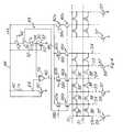
- a programming current controller as shown in Figure 2includes a resistive element 42 in a reference current leg in series with a reference ground select transistor 30 which is biased on by having its gate connected to the high voltage line Vpp 48. As a consequence of a reference current I R being established through transistor 30, a voltage V1 will be established at junction 44.
- a module programming control P-channel field effect transistor 36is in series with a module floating gate transistor 38 and an N-channel control select field effect transistor 32 identical to transistor 30, coupled between line 48 and ground. Both the transistor 38 and the transistor 32 are biased on by having their control gate 52 and gate 50, respectively, connected to line 48.
- the current 1 Ais controlled by the module programming control transistor 36 and in flowing through the control select transistor 32 develops a voltage V2 at junction 35.
- Junction 44is coupled to the inverting input of comparator 34 while junction 35 is connected to the non-inverting input thereof.
- the comparator output 40is coupled to the gate 46 of module programming control transistor 36 as well as being coupled to gates of matching array control transistors 46a, 46b, 46c, etc.
- Each of the programming control transistors 46a, 46b, etc.are coupled to corresponding column lines 54 each one of which connects to a parallel array of floating gate transistors 38 ⁇ .
- the other end of the parallel array of transistors 38 ⁇are connected to corresponding decoded ground lines 53 each of which is coupled to ground through a ground select transistor 57 the gates of which 59 are used to select the active ground line.
- reference ground select transistor 30being in a conductive state causes a current I R to flow through resistive element 42 the value of which is determined by Vpp less the voltage across transistor 30 divided by the value of resistance of element 42.
- a voltage V1 at junction 44is developed which is applied to the inverting input of comparator 34.
- the array of Figure 2may be modified as shown in Figure 4 by introducing column select transistors 60a, 60b, 60c ... etc., in respective columns 54 between V pp line 48 and respective transistors 46a, 46b, etc and P-channel transistor 47 in series with P-channel transistor 36.
- An appropriate one or more of column lines 54are selected by driving the gates 58 of column select transistors 60 low. Otherwise the operation of the circuit of Figure 4 is the same as that of Figure 2.
- Transistor 47is used to make the second leg identical to each column of the array.
Landscapes
- Read Only Memory (AREA)
- Semiconductor Memories (AREA)
Description
- The present invention relates to a programming current controlling method and device for an electrically erasable programmable semiconductor memory cell. The invention is directed, more particularly, to a programming current controlling device which is formed on a chip containing a plurality of such memory cells in an array. The invention, yet more particularly, relates to an electrically programmable semiconductor memory device having an array of floating gate transistors sets of which are coupled between associated respective source and drain lines, a array programming control transistor and a ground select transistor coupled to each of said drain and source lines such that each selected floating gate transistor in a programming mode is in series with said control and ground select transistors between a high voltage Vpp, and ground potential. Such an arrangement is exemplified in, for example, United States Patent 4,404,659.
- The programming current for an EPROM depends both on circuit elements coupled to the EPROM cell as well as on the characteristics of the EPROM cell itself. Since the programming load line normally chosen passes through a steeply sloped portion of the curve and is itself steeply sloped, any relatively small variation in the curve results in a relatively significant variation in programming current. The programming current must be maintained between an IMIN value determined by the minimum current required to program the EPROM cell and IMAX set by the Ipp specification. In the case of low programming current long programming times result whereas high programming currents may fail the specification for maximum allowable programming current.
- Advances in EPROM bit density have resulted in a trend towards shorter programming pulses per byte to minimize end user programming time per device. Because the programming time is directly proportional to the programming current there is a conflicting requirement between the need for faster programming time and the requirement to limit the maximum source/drain current to keep it below the specification maximum.
- It is therefore an object of the present invention to provide an improved method and apparatus for controlling the programming current in an array of EPROMS. It is a further object of the present invention to provide an EPROM memory device the programming of which is substantially independent of the variations in its fabrication process.
- According to the present invention there is provided an electrically programmable semiconductor memory device as set forth in
Claim 1. - The novel features believed characteristic of the invention are set forth in the appended claims. The invention itself, however, as well as other features and advantages thereof, will be best understood by reference to the detailed description which follows, read in conjunction with the accompanying drawings, wherein:
- FIG. 1 is a characteristic curve of the source/drain voltage versus source/drain current for a typical EPROM cell together with a typical programming load line;
- FIG. 2 is a schematic circuit diagram of EPROM programming current controller shown as coupled to an array of EPROM cells; and
- FIG. 3 is a schematic circuit diagram of the EPROM programming current controller;
- FIG. 4 is a schematic circuit diagram of an alternative programming current controller with column select transistors.
- Referring to Figure 1 there is shown a typical characteristic of the source/drain voltage versus the source/drain current of an EPROM memory cell. The forward path in the linear region 11, exhibits a rapid initial current rise with increasing voltage enters the
saturation region 12 and then drops off rapidly at 14 where programming begins. The drain current stays flat for a few volts and there is a sudden large linear increase in current with increasingvoltage 10. The return path followspath 10, then the long horizontal portion 16 before dropping to zero current. Atypical load line 22 is also shown in which a high voltage Vpp is applied through a programming load device. For the example shown the nominal operating point or programming current is Inom. - Shown in Figure 1 is a typical variation range of
path 10 as a result in the production tolerances of the device.Path 10 is a function of the channel length of the memory cell and is subject to up to a 2 volt variation. This will cause a range of cell programming currents from IMIN to IMAX. This change in programming current will directly affect programming time. Such a large variation in programming time creates severe production problems in terms of low yield and associated marketability. For the low current end the programming time is excessively long while for the higher current the maximum allowable programming current will be exceeded. - A programming current controller as shown in Figure 2 includes a
resistive element 42 in a reference current leg in series with a reference groundselect transistor 30 which is biased on by having its gate connected to the highvoltage line Vpp 48. As a consequence of a reference current IR being established throughtransistor 30, a voltage V₁ will be established atjunction 44. - In a second current leg, a module programming control P-channel
field effect transistor 36 is in series with a module floatinggate transistor 38 and an N-channel control selectfield effect transistor 32 identical totransistor 30, coupled betweenline 48 and ground. Both thetransistor 38 and thetransistor 32 are biased on by having theircontrol gate 52 andgate 50, respectively, connected toline 48. The current 1A is controlled by the moduleprogramming control transistor 36 and in flowing through the control selecttransistor 32 develops a voltage V₂ atjunction 35.Junction 44 is coupled to the inverting input ofcomparator 34 whilejunction 35 is connected to the non-inverting input thereof. Thecomparator output 40 is coupled to thegate 46 of moduleprogramming control transistor 36 as well as being coupled to gates of matchingarray control transistors programming control transistors corresponding column lines 54 each one of which connects to a parallel array offloating gate transistors 38´. The other end of the parallel array oftransistors 38´ are connected to corresponding decodedground lines 53 each of which is coupled to ground through a groundselect transistor 57 the gates of which 59 are used to select the active ground line. In operation reference ground selecttransistor 30 being in a conductive state causes a current IR to flow throughresistive element 42 the value of which is determined by Vpp less the voltage acrosstransistor 30 divided by the value of resistance ofelement 42. As a result of current IR flowing a voltage V1 atjunction 44 is developed which is applied to the inverting input ofcomparator 34. In the second current leg a current IA flows and as a result of passing throughtransistor 32 causes a voltage V₂ to be present atjunction 35. Thecomparator output 40 swings the voltage on thegate 46 oftransistor 36 to a value V₃ such that IA becomes substantially equal to the reference current IR. This same value of V₃ is also applied to the gates oftransistors row line 51 made by raising the voltage of that line to Vpp, there will be in series a given one oftransistors floating gate transistors 38´, and an associated one of groundselect transistors 57. The latter three circuit elements are the same as those in series in the second leg ofcurrent module 49. Since the transistors inmodule 49 are made by the same process as those in the array, the application of voltage V₃ to the gates oftransistors transistors 38´ in the array is determined by the reference current IR which, in turn, is primarily a function of resistance R ofresistive element 42. The latter can be made to relatively close tolerances and can be in the form of a bipolar transistor, N-channel or P-channel MOS transistor, or a diffusion or polysilicon resistor. - An alternative form of a module as shown in Figure 3 consists of a reference current leg made up of a reference ground select P-
channel transistor 60 in series with aresistor 61 with thetransistor 60 biased on by connection of its gate to ground thus establishing a reference current IR. The second leg consists of a P-channel control selecttransistor 68 in series with afloating gate transistor 66 biased on and a moduleprogramming control transistor 64 coupled to ground.Junction 70 oftransistor 60 andresistive element 61 is coupled to the inverting input of acomparator 62 while junction 72 oftransistor 68 andfloating gate transistor 66 is connected to the non-inverting input ofcomparator 62. The output 74 ofcomparator 62 is coupled to a gate ofmodule control transistor 64. - The operation of the circuit of Figure 3 is substantially the same as that of Figure 2 except the voltages across the P-
channel transistors module control transistor 64 is an N-channel transistor rather than a P-channel transistor. The circuit elements in the array in this case would correspond to those in the second leg of thecurrent module 69. - The array of Figure 2 may be modified as shown in Figure 4 by introducing column
select transistors respective columns 54 between Vpp line 48 andrespective transistors channel transistor 47 in series with P-channel transistor 36. An appropriate one or more ofcolumn lines 54 are selected by driving the gates 58 of column selecttransistors 60 low. Otherwise the operation of the circuit of Figure 4 is the same as that of Figure 2.Transistor 47 is used to make the second leg identical to each column of the array. - While this invention has been described with reference to an illustrative embodiment, this description is not intended to be construed in a limiting sense. Various modifications of the illustrative embodiment, as well as other embodiments of the invention, will be apparent to persons skilled in the art upon reference to this description. It is, therefore, contemplated that the appended claims will cover any such modifications or embodiments as fall within the true scope of the invention.
Claims (19)
- An electrically programmable semiconductor memory device having an array of floating gate transistors (38'), sets of which are coupled between associated respective source and drain lines (53, 54), an array programming control transistor (46a-x) and a ground select transistor (57) coupled to each of said drain and source lines such that each selected floating gate transistor in a programming mode is in series with said control and ground select transistors between a high voltage Vpp, and ground potential, characterized in that it comprises:
a resistive element (42) in series with a first resistive circuit element (30) connected between Vpp and ground whereby a voltage V₁ is established at the junction (44) of said resistive element and said first resistive circuit element;
a second resistive circuit element (32), a module floating gate transistor (38) biased into a conducting state and a module programming control transistor (46) all connected in series between Vpp and ground, whereby a voltage V₂ is established at the junction (35) of said second resistive circuit element and said module floating gate transistor; and
means (34) for comparing V₁ and V₂ and adjusting the gate voltage V₃ of said module control transistor so as to make the voltage V₂ equal to V₁ and applying V₃ to the gates of said array control transistors. - A memory device according to claim 1, wherein said first resistive circuit element and said second resistive circuit element are reference select and ground select transistors, respectively, both biased into a
- A memory device according to claim 2, wherein said comparing means is a comparator having one input coupled to the junction of said resistive element and said reference select transistor, another input coupled to the junction of said ground select transistor and said module floating gate transistor and an output coupled to the gates of said module programming control transistor and to said array programming control transistors.
- A memory device according to claim 3, wherein said semiconductor material is silicon.
- A memory device according to claim 3, wherein said module programming control and array programming control transistors are P-channel field effect transistors.
- A memory device according to claim 5, wherein said module programming control and array programming control transistors are N-channel field effect transistors.
- A memory device according to claim 4, wherein said array programming control and floating gate transistors are made by the same process as said said module programming control and module floating gate transistors.
- A memory device according to claim 3, wherein said resistive element is a bipolar transistor.
- A memory device according to claim 3, wherein said resistive element is a diffusion resistor.
- A memory device according to claim 3, wherein said resistive element is a polysilicon resistor.
- A memory device according to claim 3, wherein said resistive element is a MOS transistor.
- A method of controlling the programming current of an array of floating gate electrically programmable read only memory transistors of claim 1, comprising the steps of:
establishing a desired reference current;
comparing a voltage V₁ developed by said reference current across a circuit element in a current path to the voltage V₂ developed across a similar circuit element in another current path having similar circuit elements as those circuit elements in a path of a selected one of said array floating gate transistors;
applying V₁ to an inverting input and V₂ to a non-inverting input of a comparator and applying the comparator output to a gate of a module programming control transistor in said other current path such that the voltage across said module programming control transistor varies in response to the signal output from the comparator so as to maintain the current in said other current path substantially equal to said reference current;
and applying the comparator output to a gate of an array programming control transistor in series with the selected array floating gate transistor so as to maintain the current through the selected floating gate transistor substantially equal to the reference current. - A method according to claim 12, wherein the circuit element in the current path of said reference current, which is the same as a corresponding circuit element in said other path, is a field effect transistor.
- A method according to claim 13, wherein the circuit elements in said other current path in addition to a field effect transistor is an electrically programmable floating gate transistor and a second field effect transistor.
- A method according to claim 14, wherein circuit elements in the current path of said reference current include a resistive element in series with the field effect transistor which is biased into a conducting state.
- A method according to claim 15, wherein said resistive element is a bipolar transistor.
- A method according to claim 15, wherein said resistive element is a diffusion resistor.
- A method according to claim 15, wherein said resistive element is a polysilicon resistor.
- A method according to claim 15, wherein said resistive element is a MOS transistor.
Applications Claiming Priority (2)
| Application Number | Priority Date | Filing Date | Title |
|---|---|---|---|
| US786981 | 1985-10-15 | ||
| US06/786,981US4723225A (en) | 1985-10-15 | 1985-10-15 | Programming current controller |
Publications (3)
| Publication Number | Publication Date |
|---|---|
| EP0225441A2 EP0225441A2 (en) | 1987-06-16 |
| EP0225441A3 EP0225441A3 (en) | 1989-03-08 |
| EP0225441B1true EP0225441B1 (en) | 1992-02-19 |
Family
ID=25140103
Family Applications (1)
| Application Number | Title | Priority Date | Filing Date |
|---|---|---|---|
| EP86112823AExpiredEP0225441B1 (en) | 1985-10-15 | 1986-09-17 | Programming current controller |
Country Status (4)
| Country | Link |
|---|---|
| US (1) | US4723225A (en) |
| EP (1) | EP0225441B1 (en) |
| JP (1) | JPS62177797A (en) |
| DE (1) | DE3683930D1 (en) |
Families Citing this family (20)
| Publication number | Priority date | Publication date | Assignee | Title |
|---|---|---|---|---|
| US5367208A (en) | 1986-09-19 | 1994-11-22 | Actel Corporation | Reconfigurable programmable interconnect architecture |
| JPS6432494A (en)* | 1987-07-27 | 1989-02-02 | Mitsubishi Electric Corp | Non-volatile semiconductor storage device |
| US4868790A (en)* | 1988-04-28 | 1989-09-19 | Texas Instruments Incorporated | Reference circuit for integrated memory arrays having virtual ground connections |
| US5042009A (en)* | 1988-12-09 | 1991-08-20 | Waferscale Integration, Inc. | Method for programming a floating gate memory device |
| KR910007434B1 (en)* | 1988-12-15 | 1991-09-26 | 삼성전자 주식회사 | Eeprom and the programming method |
| US5299150A (en)* | 1989-01-10 | 1994-03-29 | Actel Corporation | Circuit for preventing false programming of anti-fuse elements |
| US5177705A (en)* | 1989-09-05 | 1993-01-05 | Texas Instruments Incorporated | Programming of an electrically-erasable, electrically-programmable, read-only memory array |
| US5027321A (en)* | 1989-11-21 | 1991-06-25 | Intel Corporation | Apparatus and method for improved reading/programming of virtual ground EPROM arrays |
| US5128895A (en)* | 1989-11-21 | 1992-07-07 | Intel Corporation | Method for programming a virtual ground EPROM cell including slow ramping of the column line voltage |
| EP0432481A3 (en)* | 1989-12-14 | 1992-04-29 | Texas Instruments Incorporated | Methods and apparatus for verifying the state of a plurality of electrically programmable memory cells |
| JP2606941B2 (en)* | 1990-02-19 | 1997-05-07 | 富士通株式会社 | Write circuit for nonvolatile memory |
| US5132933A (en)* | 1990-12-21 | 1992-07-21 | Schreck John F | Bias circuitry for nonvolatile memory array |
| US5491658A (en)* | 1991-02-13 | 1996-02-13 | Texas Instruments Incorporated | Column decoder for virtual ground memory array |
| US5719806A (en)* | 1991-02-18 | 1998-02-17 | Yamane; Masatoshi | Memory cell array |
| US5367213A (en)* | 1993-06-09 | 1994-11-22 | Micron Semiconductor, Inc. | P-channel sense amplifier pull-up circuit incorporating a voltage comparator for use in DRAM memories having non-bootstrapped word lines |
| FR2718273B1 (en)* | 1994-03-31 | 1996-05-24 | Sgs Thomson Microelectronics | Integrated memory with column voltage maintenance circuit. |
| US5481492A (en)* | 1994-12-14 | 1996-01-02 | The United States Of America As Represented By The Secretary Of The Navy | Floating gate injection voltage regulator |
| JP4715024B2 (en)* | 2001-05-08 | 2011-07-06 | セイコーエプソン株式会社 | Program method for nonvolatile semiconductor memory device |
| JP2002334588A (en)* | 2001-05-11 | 2002-11-22 | Seiko Epson Corp | Program method for nonvolatile semiconductor memory device |
| US20110002161A1 (en)* | 2009-07-06 | 2011-01-06 | Seagate Technology Llc | Phase change memory cell with selecting element |
Family Cites Families (4)
| Publication number | Priority date | Publication date | Assignee | Title |
|---|---|---|---|---|
| US4218764A (en)* | 1978-10-03 | 1980-08-19 | Matsushita Electric Industrial Co., Ltd. | Non-volatile memory refresh control circuit |
| JPS5654693A (en)* | 1979-10-05 | 1981-05-14 | Hitachi Ltd | Programable rom |
| US4387447A (en)* | 1980-02-04 | 1983-06-07 | Texas Instruments Incorporated | Column and ground select sequence in electrically programmable memory |
| NL8400661A (en)* | 1984-03-01 | 1985-10-01 | Philips Nv | SEMICONDUCTOR DEVICE WITH AT LEAST A NON-VOLATILE MEMORY TRANSISTOR. |
- 1985
- 1985-10-15USUS06/786,981patent/US4723225A/ennot_activeExpired - Lifetime
- 1986
- 1986-09-17DEDE8686112823Tpatent/DE3683930D1/ennot_activeExpired - Lifetime
- 1986-09-17EPEP86112823Apatent/EP0225441B1/ennot_activeExpired
- 1986-10-14JPJP61244006Apatent/JPS62177797A/enactiveGranted
Also Published As
| Publication number | Publication date |
|---|---|
| JPS62177797A (en) | 1987-08-04 |
| US4723225A (en) | 1988-02-02 |
| EP0225441A3 (en) | 1989-03-08 |
| JPH0529996B2 (en) | 1993-05-06 |
| EP0225441A2 (en) | 1987-06-16 |
| DE3683930D1 (en) | 1992-03-26 |
Similar Documents
| Publication | Publication Date | Title |
|---|---|---|
| EP0225441B1 (en) | Programming current controller | |
| US5218571A (en) | EPROM source bias circuit with compensation for processing characteristics | |
| US5253201A (en) | Writing control circuit employed in non-volatile semiconductor memory device | |
| US5142495A (en) | Variable load for margin mode | |
| US5706240A (en) | Voltage regulator for memory device | |
| US5406141A (en) | High voltage CMOS switching circuit | |
| US4874967A (en) | Low power voltage clamp circuit | |
| JPH04132088A (en) | High voltage generation circuit for semiconductor memory element and eeprom | |
| EP0729633B1 (en) | Sense amplifier for non-volatile semiconductor memory | |
| US5905677A (en) | Voltage regulator for non-volatile semiconductor electrically programmable memory devices | |
| JP2851035B2 (en) | Programmable logic device | |
| US4843594A (en) | Nonvolatile semiconductor memory device with a bias circuit | |
| KR100322471B1 (en) | A sense amplifier circuit for use in a nonvolatile semiconductor memory device | |
| US5117392A (en) | Non-volatile semiconductor memory device | |
| US5872733A (en) | Ramp-up rate control circuit for flash memory charge pump | |
| JPH05102402A (en) | Semiconductor device | |
| KR100382037B1 (en) | Semiconductor memory device with constant voltage circuit | |
| EP0225442B1 (en) | Equalized biased array for proms and eproms | |
| EP0183476B1 (en) | Mos read-only memory systems | |
| US5488586A (en) | Method and apparatus for erasing an array of electrically erasable programmable read only memory cells | |
| US5691944A (en) | Non-volatile semiconductor memory device | |
| KR19990071743A (en) | High Voltage Level Shifting CMOS Buffer | |
| EP0346671B1 (en) | EPROM programming | |
| EP0757358B1 (en) | A circuit for reading non-volatile memories | |
| US5617370A (en) | Semiconductor memory device with controllable charging characteristics of column lines |
Legal Events
| Date | Code | Title | Description |
|---|---|---|---|
| PUAI | Public reference made under article 153(3) epc to a published international application that has entered the european phase | Free format text:ORIGINAL CODE: 0009012 | |
| AK | Designated contracting states | Kind code of ref document:A2 Designated state(s):DE FR GB | |
| PUAL | Search report despatched | Free format text:ORIGINAL CODE: 0009013 | |
| AK | Designated contracting states | Kind code of ref document:A3 Designated state(s):DE FR GB | |
| 17P | Request for examination filed | Effective date:19890721 | |
| 17Q | First examination report despatched | Effective date:19901128 | |
| GRAA | (expected) grant | Free format text:ORIGINAL CODE: 0009210 | |
| AK | Designated contracting states | Kind code of ref document:B1 Designated state(s):DE FR GB | |
| REF | Corresponds to: | Ref document number:3683930 Country of ref document:DE Date of ref document:19920326 | |
| ET | Fr: translation filed | ||
| PLBE | No opposition filed within time limit | Free format text:ORIGINAL CODE: 0009261 | |
| STAA | Information on the status of an ep patent application or granted ep patent | Free format text:STATUS: NO OPPOSITION FILED WITHIN TIME LIMIT | |
| 26N | No opposition filed | ||
| REG | Reference to a national code | Ref country code:GB Ref legal event code:IF02 | |
| PGFP | Annual fee paid to national office [announced via postgrant information from national office to epo] | Ref country code:DE Payment date:20030930 Year of fee payment:18 | |
| PG25 | Lapsed in a contracting state [announced via postgrant information from national office to epo] | Ref country code:DE Free format text:LAPSE BECAUSE OF NON-PAYMENT OF DUE FEES Effective date:20050401 | |
| PGFP | Annual fee paid to national office [announced via postgrant information from national office to epo] | Ref country code:GB Payment date:20050809 Year of fee payment:20 | |
| PGFP | Annual fee paid to national office [announced via postgrant information from national office to epo] | Ref country code:FR Payment date:20050902 Year of fee payment:20 | |
| PG25 | Lapsed in a contracting state [announced via postgrant information from national office to epo] | Ref country code:GB Free format text:LAPSE BECAUSE OF EXPIRATION OF PROTECTION Effective date:20060916 | |
| REG | Reference to a national code | Ref country code:GB Ref legal event code:PE20 |