EP0213974B1 - Micromodule with embedded contacts and a card containing circuits comprising such a micromodule - Google Patents
Micromodule with embedded contacts and a card containing circuits comprising such a micromoduleDownload PDFInfo
- Publication number
- EP0213974B1 EP0213974B1EP19860401296EP86401296AEP0213974B1EP 0213974 B1EP0213974 B1EP 0213974B1EP 19860401296EP19860401296EP 19860401296EP 86401296 AEP86401296 AEP 86401296AEP 0213974 B1EP0213974 B1EP 0213974B1
- Authority
- EP
- European Patent Office
- Prior art keywords
- micromodule
- card
- microcircuit
- conductive parts
- film
- Prior art date
- Legal status (The legal status is an assumption and is not a legal conclusion. Google has not performed a legal analysis and makes no representation as to the accuracy of the status listed.)
- Expired - Lifetime
Links
Images
Classifications
- G—PHYSICS
- G06—COMPUTING OR CALCULATING; COUNTING
- G06K—GRAPHICAL DATA READING; PRESENTATION OF DATA; RECORD CARRIERS; HANDLING RECORD CARRIERS
- G06K19/00—Record carriers for use with machines and with at least a part designed to carry digital markings
- G06K19/06—Record carriers for use with machines and with at least a part designed to carry digital markings characterised by the kind of the digital marking, e.g. shape, nature, code
- G06K19/067—Record carriers with conductive marks, printed circuits or semiconductor circuit elements, e.g. credit or identity cards also with resonating or responding marks without active components
- G06K19/07—Record carriers with conductive marks, printed circuits or semiconductor circuit elements, e.g. credit or identity cards also with resonating or responding marks without active components with integrated circuit chips
- G06K19/077—Constructional details, e.g. mounting of circuits in the carrier
- G06K19/07745—Mounting details of integrated circuit chips
- G06K19/07747—Mounting details of integrated circuit chips at least one of the integrated circuit chips being mounted as a module
- G—PHYSICS
- G06—COMPUTING OR CALCULATING; COUNTING
- G06K—GRAPHICAL DATA READING; PRESENTATION OF DATA; RECORD CARRIERS; HANDLING RECORD CARRIERS
- G06K19/00—Record carriers for use with machines and with at least a part designed to carry digital markings
- G06K19/06—Record carriers for use with machines and with at least a part designed to carry digital markings characterised by the kind of the digital marking, e.g. shape, nature, code
- G06K19/067—Record carriers with conductive marks, printed circuits or semiconductor circuit elements, e.g. credit or identity cards also with resonating or responding marks without active components
- G06K19/07—Record carriers with conductive marks, printed circuits or semiconductor circuit elements, e.g. credit or identity cards also with resonating or responding marks without active components with integrated circuit chips
- G06K19/077—Constructional details, e.g. mounting of circuits in the carrier
- G06K19/07745—Mounting details of integrated circuit chips
- H—ELECTRICITY
- H01—ELECTRIC ELEMENTS
- H01L—SEMICONDUCTOR DEVICES NOT COVERED BY CLASS H10
- H01L23/00—Details of semiconductor or other solid state devices
- H01L23/48—Arrangements for conducting electric current to or from the solid state body in operation, e.g. leads, terminal arrangements ; Selection of materials therefor
- H01L23/488—Arrangements for conducting electric current to or from the solid state body in operation, e.g. leads, terminal arrangements ; Selection of materials therefor consisting of soldered or bonded constructions
- H01L23/498—Leads, i.e. metallisations or lead-frames on insulating substrates, e.g. chip carriers
- H01L23/49855—Leads, i.e. metallisations or lead-frames on insulating substrates, e.g. chip carriers for flat-cards, e.g. credit cards
- H—ELECTRICITY
- H01—ELECTRIC ELEMENTS
- H01L—SEMICONDUCTOR DEVICES NOT COVERED BY CLASS H10
- H01L23/00—Details of semiconductor or other solid state devices
- H01L23/52—Arrangements for conducting electric current within the device in operation from one component to another, i.e. interconnections, e.g. wires, lead frames
- H01L23/538—Arrangements for conducting electric current within the device in operation from one component to another, i.e. interconnections, e.g. wires, lead frames the interconnection structure between a plurality of semiconductor chips being formed on, or in, insulating substrates
- H01L23/5384—Conductive vias through the substrate with or without pins, e.g. buried coaxial conductors
- H—ELECTRICITY
- H01—ELECTRIC ELEMENTS
- H01L—SEMICONDUCTOR DEVICES NOT COVERED BY CLASS H10
- H01L2224/00—Indexing scheme for arrangements for connecting or disconnecting semiconductor or solid-state bodies and methods related thereto as covered by H01L24/00
- H01L2224/01—Means for bonding being attached to, or being formed on, the surface to be connected, e.g. chip-to-package, die-attach, "first-level" interconnects; Manufacturing methods related thereto
- H01L2224/42—Wire connectors; Manufacturing methods related thereto
- H01L2224/47—Structure, shape, material or disposition of the wire connectors after the connecting process
- H01L2224/48—Structure, shape, material or disposition of the wire connectors after the connecting process of an individual wire connector
- H01L2224/4805—Shape
- H01L2224/4809—Loop shape
- H01L2224/48091—Arched
- H—ELECTRICITY
- H01—ELECTRIC ELEMENTS
- H01L—SEMICONDUCTOR DEVICES NOT COVERED BY CLASS H10
- H01L2224/00—Indexing scheme for arrangements for connecting or disconnecting semiconductor or solid-state bodies and methods related thereto as covered by H01L24/00
- H01L2224/01—Means for bonding being attached to, or being formed on, the surface to be connected, e.g. chip-to-package, die-attach, "first-level" interconnects; Manufacturing methods related thereto
- H01L2224/42—Wire connectors; Manufacturing methods related thereto
- H01L2224/47—Structure, shape, material or disposition of the wire connectors after the connecting process
- H01L2224/48—Structure, shape, material or disposition of the wire connectors after the connecting process of an individual wire connector
- H01L2224/481—Disposition
- H01L2224/48151—Connecting between a semiconductor or solid-state body and an item not being a semiconductor or solid-state body, e.g. chip-to-substrate, chip-to-passive
- H01L2224/48221—Connecting between a semiconductor or solid-state body and an item not being a semiconductor or solid-state body, e.g. chip-to-substrate, chip-to-passive the body and the item being stacked
- H01L2224/48225—Connecting between a semiconductor or solid-state body and an item not being a semiconductor or solid-state body, e.g. chip-to-substrate, chip-to-passive the body and the item being stacked the item being non-metallic, e.g. insulating substrate with or without metallisation
- H01L2224/48227—Connecting between a semiconductor or solid-state body and an item not being a semiconductor or solid-state body, e.g. chip-to-substrate, chip-to-passive the body and the item being stacked the item being non-metallic, e.g. insulating substrate with or without metallisation connecting the wire to a bond pad of the item
- H—ELECTRICITY
- H01—ELECTRIC ELEMENTS
- H01L—SEMICONDUCTOR DEVICES NOT COVERED BY CLASS H10
- H01L2224/00—Indexing scheme for arrangements for connecting or disconnecting semiconductor or solid-state bodies and methods related thereto as covered by H01L24/00
- H01L2224/01—Means for bonding being attached to, or being formed on, the surface to be connected, e.g. chip-to-package, die-attach, "first-level" interconnects; Manufacturing methods related thereto
- H01L2224/42—Wire connectors; Manufacturing methods related thereto
- H01L2224/47—Structure, shape, material or disposition of the wire connectors after the connecting process
- H01L2224/48—Structure, shape, material or disposition of the wire connectors after the connecting process of an individual wire connector
- H01L2224/484—Connecting portions
- H01L2224/4847—Connecting portions the connecting portion on the bonding area of the semiconductor or solid-state body being a wedge bond
- H01L2224/48472—Connecting portions the connecting portion on the bonding area of the semiconductor or solid-state body being a wedge bond the other connecting portion not on the bonding area also being a wedge bond, i.e. wedge-to-wedge
- H—ELECTRICITY
- H01—ELECTRIC ELEMENTS
- H01L—SEMICONDUCTOR DEVICES NOT COVERED BY CLASS H10
- H01L2224/00—Indexing scheme for arrangements for connecting or disconnecting semiconductor or solid-state bodies and methods related thereto as covered by H01L24/00
- H01L2224/73—Means for bonding being of different types provided for in two or more of groups H01L2224/10, H01L2224/18, H01L2224/26, H01L2224/34, H01L2224/42, H01L2224/50, H01L2224/63, H01L2224/71
- H01L2224/732—Location after the connecting process
- H01L2224/73251—Location after the connecting process on different surfaces
- H01L2224/73265—Layer and wire connectors
- H—ELECTRICITY
- H01—ELECTRIC ELEMENTS
- H01L—SEMICONDUCTOR DEVICES NOT COVERED BY CLASS H10
- H01L24/00—Arrangements for connecting or disconnecting semiconductor or solid-state bodies; Methods or apparatus related thereto
- H01L24/01—Means for bonding being attached to, or being formed on, the surface to be connected, e.g. chip-to-package, die-attach, "first-level" interconnects; Manufacturing methods related thereto
- H01L24/42—Wire connectors; Manufacturing methods related thereto
- H01L24/47—Structure, shape, material or disposition of the wire connectors after the connecting process
- H01L24/48—Structure, shape, material or disposition of the wire connectors after the connecting process of an individual wire connector
- H—ELECTRICITY
- H01—ELECTRIC ELEMENTS
- H01L—SEMICONDUCTOR DEVICES NOT COVERED BY CLASS H10
- H01L2924/00—Indexing scheme for arrangements or methods for connecting or disconnecting semiconductor or solid-state bodies as covered by H01L24/00
- H01L2924/0001—Technical content checked by a classifier
- H01L2924/00014—Technical content checked by a classifier the subject-matter covered by the group, the symbol of which is combined with the symbol of this group, being disclosed without further technical details
- H—ELECTRICITY
- H01—ELECTRIC ELEMENTS
- H01L—SEMICONDUCTOR DEVICES NOT COVERED BY CLASS H10
- H01L2924/00—Indexing scheme for arrangements or methods for connecting or disconnecting semiconductor or solid-state bodies as covered by H01L24/00
- H01L2924/01—Chemical elements
- H01L2924/01014—Silicon [Si]
- H—ELECTRICITY
- H01—ELECTRIC ELEMENTS
- H01L—SEMICONDUCTOR DEVICES NOT COVERED BY CLASS H10
- H01L2924/00—Indexing scheme for arrangements or methods for connecting or disconnecting semiconductor or solid-state bodies as covered by H01L24/00
- H01L2924/01—Chemical elements
- H01L2924/01057—Lanthanum [La]
- H—ELECTRICITY
- H01—ELECTRIC ELEMENTS
- H01L—SEMICONDUCTOR DEVICES NOT COVERED BY CLASS H10
- H01L2924/00—Indexing scheme for arrangements or methods for connecting or disconnecting semiconductor or solid-state bodies as covered by H01L24/00
- H01L2924/01—Chemical elements
- H01L2924/01079—Gold [Au]
- H—ELECTRICITY
- H01—ELECTRIC ELEMENTS
- H01L—SEMICONDUCTOR DEVICES NOT COVERED BY CLASS H10
- H01L2924/00—Indexing scheme for arrangements or methods for connecting or disconnecting semiconductor or solid-state bodies as covered by H01L24/00
- H01L2924/15—Details of package parts other than the semiconductor or other solid state devices to be connected
- H01L2924/181—Encapsulation
Definitions
- the present inventionrelates to a micromodule with buried contacts. It also relates to a CCC type card containing circuits comprising such a micromodule. It finds application in the fields of electronic payment or security.
- CCCa special card containing an electronic microcircuit.
- the microcircuitcan consist of a writable memory, a read only memory and up to a microcomputer in the case of high level CCC cards. It is known to constitute the CCC card in at least two parts. The first part consists of the plastic card itself. A second part consists of a micromodule comprising a support, electrical contacts and at least one microcircuit connected to said contacts and fixed to the support.
- micromodule of the prior art described thereincomprises a substrate, lateral and central conductive areas formed on the external face of the substrate.
- the arrangement describedhas drawbacks. Indeed, once the micromodule installed on the plastic card proper, according to this state of the art, the microcircuit installed on the substrate is invisible from the outside. Also found from the outside to the inside of the card first of all the conductive parts constituting in particular the contacts, a substrate for example of PVC type then the microcircuit connected by wires to the lateral conductive areas.
- a well dug inside the PVC substrateallows to stick the microcircuit on the internal face of the central conductive part.
- the connecting wires of the microcircuitare arranged inside transverse perforations of the substrate and fixed on the lateral conductive pads.
- Such cardsare subject to risks of deterioration of the metal parts. Indeed, it will be noted that the dimensions of the card are very small.
- the metallic filmis of the order of 60 microns thick.
- the cardis inserted into a reader.
- the contactsare connected to the reader by a friction connector. When removing the card, the contacts being hot, there is a risk of damage to the contacts.
- Another drawback of this arrangementis that the card is intended to be handled in sometimes extreme conditions.
- the cardcan be bent, which constitutes a risk of detachment of the metal parts.
- the inventionprovides a micromodule as defined in claims 1 and 4.
- the conductive partsare arranged on the internal face of a plastic support.
- a microcircuitis arranged on the internal face of a central conductive part and wires for connection of this microcircuit to lateral conductive parts are provided. Perforations in the plastic support allow contact areas to be provided in predetermined locations.
- the inventionalso makes it possible to avoid drilling a central well in the plastic support to house the microcircuit on the internal face of the central metal.
- the inventionalso relates to a card as defined in claim 5.
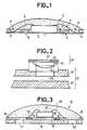
- FIG. 1there is shown a micromodule formed according to the prior art.
- a microcircuit 1is placed on a metallic film 2.
- the metallic filminitially consists of an etched strip so as to arrange a central part 2 which receives the microcircuit 1 and lateral parts 3, 4, which will receive the ends of connections 5, 6 of the chip.
- the metal strip 2 - 4is bonded to the external face of a plastic film constituting a material support for the micromodule.
- This plastic filmis pierced with two kinds of holes.
- a first kind of holeis constituted by a hole 7 or well in which is disposed the microcircuit 1.
- This wellis compulsory in this process of the prior art to provide a rear connection of the microcircuit. This is particularly the case for microcircuits with substrate polarization, in particular silicon.
- Another kind of drillingis constituted by the holes 10 and 11 which make it possible to bring the connection wires 6 and 5 to the lateral conductive parts 3 and 4.
- the conductive wires 5, 6are fixed by welding or gluing on the internal face of the conductive strip.
- the internal face of the micromodule, upper in the drawingis embedded in a bead of protective resin 12 deposited hot.
- FIG. 2there is shown the inserting operation of the micromodule.
- the micromodule 20consisting of the conductive parts of external contact 22, of the support 23 and of the drop of resin 25 is firstly shaped according to the dotted lines 24 so as to be able to be placed on a plastic wedge 26.
- the chip and the drop of resinare formed along the dotted line 24 by machining and are placed in the housing 28 of the wedge 26.
- the base 27is made of the same material as the wedge 26.
- the assemblycan be assembled by gluing or by heating.
- the card 21therefore has three main parts: a micromodule 20, a wedge 26 and a base 27.
- FIG. 3there is shown a micromodule formed according to the invention.
- the plastic film which constitutes the support of the micromoduleis placed outside the card after insertion.
- the conductive stripis arranged, made up of central conductive parts 32 and lateral 33 and 34.
- the microcircuit 37is placed on the central part 32 and the connection wires 35 and 36 are soldered or fixed directly to the internal face of the lateral conductive parts 33, 34.
- the electrical mounting processrequires no manipulation or shaping of the plastic support 31.
- the conductive areas 32, 33 and 34are separated by insulating parts 39, 40 in the drawing.
- insulating parts 39, 40In reality, a standard emerged according to which eight contacts are planned. Eight separate conductive parts must therefore be cut.
- Each conductive part in one embodimentis separated from the next by an insulating part such as part 39 or part 40 of FIG. 3.
- the insulating partscan be simple cutouts between conductive parts or even insulating bars.
- electrically insulating parts 39, 40are chosen which have the role of dissipating the thermal energy released by the circuit.
- the insulating partsare cutouts made by photoengraving of a metal strip. A photogravure cutting process ensures the possibility of continuous manufacturing of the micromodule.
- the microcircuit 37 in one embodimentis disposed on the central conductive part 32 by means of a layer of conductive adhesive 38.
- the central conductive part 32is formed by metallization of the rear face of the microcircuit 37.
- the microcircuitcomprises a substrate for example in doped silicon which must be polarized by an electrode on the rear face of the substrate.
- the location of the contactsis predetermined.
- the inventionhas the remarkable feature that it makes it possible to adjust this contact area only by drilling a plastic film 31.
- the holes 41, 42which are the usual standard eight in number , are provided with a metallization which favors the reading of the contacts which are buried inside the support film.
- the conductive parts 32 - 34are fixed to the plastic support 31 by gluing. In another embodiment, the conductive parts are fixed to the support by heating or by pressing.
- the micromodule of the inventionis particularly suitable for constituting a component of a card containing a circuit of the CCC type.
Landscapes
- Engineering & Computer Science (AREA)
- Computer Hardware Design (AREA)
- Microelectronics & Electronic Packaging (AREA)
- Physics & Mathematics (AREA)
- General Physics & Mathematics (AREA)
- Condensed Matter Physics & Semiconductors (AREA)
- Power Engineering (AREA)
- Theoretical Computer Science (AREA)
- Credit Cards Or The Like (AREA)
- Parts Printed On Printed Circuit Boards (AREA)
- Wire Bonding (AREA)
Description
Translated fromFrenchLa présente invention concerne un micromodule à contacts enterrés. Elle concerne aussi une carte de type CCC contenant des circuits comportant un tel micromodule. Elle trouve application dans les domaines du paiement électronique ou encore de la sécurité.The present invention relates to a micromodule with buried contacts. It also relates to a CCC type card containing circuits comprising such a micromodule. It finds application in the fields of electronic payment or security.
De l'art antérieur, il est connu de constituer sur une carte plastique une carte spéciale contenant un microcircuit électronique. Cette carte désignée sous le vocable CCC respecte un format standard décrivant les cartes de crédit. Le microcircuit peut être constitué par une mémoire inscriptible, une mémoire morte et jusqu'à un microordinateur dans le cas de cartes CCC de haut niveau. Il est connu de constituer la carte CCC en au moins deux parties. Une première partie est constituée par la carte plastique proprement dite. Une seconde partie est constituée par un micromodule comportant un support, des contacts électriques et au moins un microcircuit relié auxdits contacts et fixé au support.From the prior art, it is known to constitute on a plastic card a special card containing an electronic microcircuit. This card, designated CCC, follows a standard format describing credit cards. The microcircuit can consist of a writable memory, a read only memory and up to a microcomputer in the case of high level CCC cards. It is known to constitute the CCC card in at least two parts. The first part consists of the plastic card itself. A second part consists of a micromodule comprising a support, electrical contacts and at least one microcircuit connected to said contacts and fixed to the support.
Dans le brevet français 2.548.857, on a indiqué un procédé de fabrication d'un micromodule spécialement destiné à une fabrication en continu d'une carte imprimée tout à fait comparable au micromodule de l'invention. Le micromodule de l'art antérieur qui y est décrit comporte un substrat, des plages conductrices latérales et centrale ménagées sur la face externe du substrat. Mais la disposition décrite présente des inconvénients. En effet, une fois le micromodule installé sur la carte plastique proprement dite, selon cet état de l'art, le microcircuit installé sur le substrat est invisible de l'extérieur. Aussi on trouve de l'extérieur vers l'intérieur de la carte tout d'abord les parties conductrices constituant notamment les contacts, un substrat par exemple de genre PVC puis le microcircuit relié par des fils aux zones conductrices latérales. Un puits creusé à l'intérieur du substrat PVC permet de coller le microcircuit sur la face interne de la partie conductrice centrale. Les fils de raccordement du microcircuit sont disposés à l'intérieur de perforations transversales du substrat et fixés sur les plages conductrices latérales. De telles cartes sont soumises à des risques de détérioration des parties métalliques. En effet on notera que les dimensions de la carte sont très faibles. Le film métallique est de l'ordre de 60 microns d'épaisseur. En opération, la carte est introduite dans un lecteur. Les contacts sont reliés au lecteur par un connecteur par frottement. Au retrait de la carte, les contacts étant chauds, il existe un risque de détérioration des contacts. Un autre inconvénient de cette disposition réside en ce que la carte est destinée à être manipulée dans des conditions parfois extremes. En particulier la carte peut être tordue, ce qui constitue un risque de décollement des parties métalliques. Afin de porter remède à ces inconvénients de l'art antérieur tout en ménageant les avantages d'une construction en continu de micromodules, l'invention propose un micromodule tel que défini dans les revendications 1 et 4. Dans ce micromodule, les parties conductrices sont disposées sur la face interne d'un support plastique. Un microcircuit est disposé sur la face interne d'une partie conductrice centrale et des fils de connexion de ce microcircuit à des parties conductrices latérales sont prévues. Des perforations dans le support plastique permettent de ménager des zones de contact dans des endroits prédéterminés.In French patent 2,548,857, a process for the manufacture of a micromodule specially intended for the continuous manufacture of a printed card is indicated, quite comparable to the micromodule of the invention. The micromodule of the prior art described therein comprises a substrate, lateral and central conductive areas formed on the external face of the substrate. However, the arrangement described has drawbacks. Indeed, once the micromodule installed on the plastic card proper, according to this state of the art, the microcircuit installed on the substrate is invisible from the outside. Also found from the outside to the inside of the card first of all the conductive parts constituting in particular the contacts, a substrate for example of PVC type then the microcircuit connected by wires to the lateral conductive areas. A well dug inside the PVC substrate allows to stick the microcircuit on the internal face of the central conductive part. The connecting wires of the microcircuit are arranged inside transverse perforations of the substrate and fixed on the lateral conductive pads. Such cards are subject to risks of deterioration of the metal parts. Indeed, it will be noted that the dimensions of the card are very small. The metallic film is of the order of 60 microns thick. In operation, the card is inserted into a reader. The contacts are connected to the reader by a friction connector. When removing the card, the contacts being hot, there is a risk of damage to the contacts. Another drawback of this arrangement is that the card is intended to be handled in sometimes extreme conditions. In particular, the card can be bent, which constitutes a risk of detachment of the metal parts. In order to remedy these drawbacks of the prior art while providing the advantages of a continuous construction of micromodules, the invention provides a micromodule as defined in claims 1 and 4. In this micromodule, the conductive parts are arranged on the internal face of a plastic support. A microcircuit is arranged on the internal face of a central conductive part and wires for connection of this microcircuit to lateral conductive parts are provided. Perforations in the plastic support allow contact areas to be provided in predetermined locations.
On notera par ailleurs qu'il est connu du document FR 2 439 438, un micromodule dans lequel les parties conductrices servant de contacts de la carte sont disposées sur la face externe du support plastique et sont donc soumis aux risques de détérioration que l'invention évite.Note also that it is known from document FR 2 439 438, a micromodule in which the conductive parts serving as contacts of the card are arranged on the external face of the plastic support and are therefore subject to the risks of deterioration that the invention avoid.
On remarquera que l'invention permet aussi d'éviter de percer un puits central dans le support plastique pour loger le microcircuit sur la face interne du métal central.It will be noted that the invention also makes it possible to avoid drilling a central well in the plastic support to house the microcircuit on the internal face of the central metal.
L'invention concerne aussi une carte telle que définie dans la revendication 5.The invention also relates to a card as defined in
D'autres avantages et caractéristiques de la présente invention seront mieux compris à l'aide de la description et des figures annexées qui sont :
- la figure 1 une coupe schématique d'un micromodule constitué selon l'art antérieur,
- la figure 2 un schéma de montage d'un micromodule sur une carte CCC,
- la figure 3 une coupe schématique d'un micromodule selon l'invention.
- FIG. 1 a schematic section of a micromodule constituted according to the prior art,
- FIG. 2, a diagram of mounting a micromodule on a CCC card,
- Figure 3 a schematic section of a micromodule according to the invention.
A la figure 1 on a représenté un micromodule constitué selon l'art antérieur. Un microcircuit 1 est disposé sur un film métallique 2. Le film métallique est constitué initialement par une bande gravée de façon à aménager une partie centrale 2 qui reçoit le microcircuit 1 et des parties latérales 3, 4, qui recevront les extrêmités de connexions 5, 6 de la puce. La bande métallique 2 - 4 est collée sur la face externe d'un film plastique constituant un support matériel au micromodule. Ce film plastique est percé de deux genres de trous. Un premier genre de trous est constitué par un trou 7 ou puits dans lequel est disposé le microcircuit 1. Ce puits est obligatoire dans ce procédé de l'art antérieur pour ménager une connexion arrière du microcircuit. C'est notamment le cas des microcircuits à polarisation de substrat, silicium notamment. Un autre genre de perçage est constitué par les perçage 10 et 11 qui permettent d'amener les fils de connexions 6 et 5 aux parties conductrices latérales 3 et 4. Les fils conducteurs 5, 6 sont fixés par soudage ou collage sur la face interne de la bande conductrice. A la fin du procédé de montage, la face interne du micromodule, supérieure sur le dessin, est noyée dans une perle de résine de protection 12 déposée à chaud. En utilisant des matériaux PVC pour le film et la résine de protection, on obtient une bonne constitution mécanique du microcircuit.In Figure 1 there is shown a micromodule formed according to the prior art. A microcircuit 1 is placed on a metallic film 2. The metallic film initially consists of an etched strip so as to arrange a central part 2 which receives the microcircuit 1 and lateral parts 3, 4, which will receive the ends of
A la figure 2 on a représenté l'opération d'encartage du micromodule. Le micromodule 20 constitué des parties conductrices de contact externe 22, du support 23 et de la goutte de résine 25 est tout d'abord mise en forme selon les traits pointillés 24 de manière à pouvoir se placer sur une cale en plastique 26. La puce et la goutte de résine sont formées selon le pointillé 24 par usinage et viennent se disposer dans le logement 28 de la cale 26. L'embase 27 est réalisée dans le même matériau que la cale 26. L'ensemble peut être assemblé par collage ou encore par chauffage. La carte 21 comporte donc trois parties principales : un micromodule 20, une cale 26 et une embase 27.In Figure 2 there is shown the inserting operation of the micromodule. The
A la figure 3, on a représenté un micromodule constitué selon l'invention. Contrairement à l'art antérieur, le film plastique qui constitue le support du micromodule est disposé à l'extérieur de la carte après encartage. Sur sa face interne, est disposée la bande conductrice constituée en parties conductrices centrale 32 et latérales 33 et 34. Le microcircuit 37 est disposé sur la partie centrale 32 et les fils de connexions 35 et 36 sont soudés ou fixés directement sur la face interne des parties conductrices latérales 33, 34. A ce niveau de la description, on constate immédiatement que le procédé de montage électrique ne requièrt aucune manipulation ni aucun façonnage du support plastique 31.In Figure 3, there is shown a micromodule formed according to the invention. Unlike the prior art, the plastic film which constitutes the support of the micromodule is placed outside the card after insertion. On its internal face, the conductive strip is arranged, made up of central
Les zones conductrices 32, 33 et 34 sont séparées par des parties isolantes 39, 40 au dessin. Dans la réalité un standard s'est dégagé selon lequel huit contacts sont prévus. Il faut donc découper huit parties conductrices distinctes. Chaque partie conductrice dans un mode d'exécution est séparée de la suivante par une partie isolante comme la partie 39 ou la partie 40 de la figure 3. Les parties isolantes peuvent être des simples découpes entre parties conductrices ou encore des barrettes isolantes. Dans un mode d'exécution on choisit des parties électriquement isolantes 39, 40 ayant un rôle de dissipation de l'énergie thermique dégagée par le circuit. Dans un autre mode de réalisation, les parties isolantes sont des découpes réalisées par photogravure d'une bande métallique. Un procédé de découpe par photogravure assure la possibilité d'une fabrication continue du micromodule.The
Le microcircuit 37 dans un mode de réalisation est disposé sur la partie centrale conductrice 32 par l'intermédiaire d'une couche de colle conductrice 38. Dans un autre mode de réalisation, la partie centrale conductrice 32 est constituée par une métallisation de la face arrière du microcircuit 37. Une telle façon est particulièrement intéressante quand le microcircuit comporte un substrat par exemple en silicium dopé qu'il faut polariser par une électrode de face arrière de substrat.The microcircuit 37 in one embodiment is disposed on the central
Dans le standard qui régit la constitution des cartes CCC au format "carte de crédit", la localisation des contacts est prédéterminée. L'invention a ceci de remarquable qu'elle permet d'ajuster cette zone de contacts uniquement par perçage d'un film plastique 31. Dans un autre mode de réalisation, les perçages 41, 42, qui sont au standard habituel au nombre de huit, sont munis d'une métallisation qui favorise la lecture des contacts qui sont enterrés à l'intérieur du film support.In the standard which governs the constitution of CCC cards in "credit card" format, the location of the contacts is predetermined. The invention has the remarkable feature that it makes it possible to adjust this contact area only by drilling a
Dans un mode de réalisation, les parties conductrices 32 - 34 sont fixées au support plastique 31 par collage. Dans un autre mode de réalisation, les parties conductrices sont fixées au support par chauffage ou par pressage.In one embodiment, the conductive parts 32 - 34 are fixed to the
Le micromodule de l'invention est particulièrement adapté à constituer un composant d'une carte contenant un circuit d'un type CCC.The micromodule of the invention is particularly suitable for constituting a component of a card containing a circuit of the CCC type.
Claims (5)
- Micromodule intended to be mounted in a card containing a microcircuit, comprising a plastic main support film (31) having an inner face and an outer face, the inner face being embedded in the card after insertion of the micromodule and the outer face being deposited towards the outside of the card after insertion, central (32) and lateral (33, 34) conductive parts being deposited on the inner face of the film, an electronic microcircuit (37) being disposed on the central conductive part on the same side as the card and being connected to the lateral conductive parts by connecting wires (35, 36), characterised in that it comprises access perforations (41, 42) provided in the film opposite the lateral conductive parts in order to provide contact areas through the access perforations.
- Micromodule according to Claim 1, characterised in that the conductive parts are produced by cutting out a metal strip which is then bonded to or pressed onto the support film.
- Micromodule according to one of the preceding claims, characterised in that the access perforations are metallised.
- Micromodule intended to be mounted in a card containing a microcircuit, comprising a plastic main support film (31) having an inner face and an outer face, the inner face being embedded in the card after insertion of the micromodule and the outer face being disposed towards the outside of the card after insertion, lateral conductive parts being deposited on the inner face of the film, and a central conductive part being formed by metallisation of the rear face of a microcircuit (37) disposed on the film on the same side as the card and connected to the lateral conductive parts by connecting wires, characterised in that it comprises access perforations (41, 42) formed in the film opposite the lateral conductive parts in order to form contact areas through the access perforations.
- Card including a microcircuit, characterised in that it includes a micromodule according to one of the preceding claims, the lateral conductive parts being accessible from the outer face of the support film.
Applications Claiming Priority (2)
| Application Number | Priority Date | Filing Date | Title |
|---|---|---|---|
| FR8509074 | 1985-06-14 | ||
| FR8509074AFR2583574B1 (en) | 1985-06-14 | 1985-06-14 | MICROMODULE WITH BURIAL CONTACTS AND CARD CONTAINING CIRCUITS COMPRISING SUCH A MICROMODULE. |
Publications (2)
| Publication Number | Publication Date |
|---|---|
| EP0213974A1 EP0213974A1 (en) | 1987-03-11 |
| EP0213974B1true EP0213974B1 (en) | 1995-02-08 |
Family
ID=9320266
Family Applications (1)
| Application Number | Title | Priority Date | Filing Date |
|---|---|---|---|
| EP19860401296Expired - LifetimeEP0213974B1 (en) | 1985-06-14 | 1986-06-13 | Micromodule with embedded contacts and a card containing circuits comprising such a micromodule |
Country Status (4)
| Country | Link |
|---|---|
| EP (1) | EP0213974B1 (en) |
| JP (1) | JPS61291194A (en) |
| DE (1) | DE3650227T2 (en) |
| FR (1) | FR2583574B1 (en) |
Families Citing this family (10)
| Publication number | Priority date | Publication date | Assignee | Title |
|---|---|---|---|---|
| JP2904785B2 (en)* | 1987-01-26 | 1999-06-14 | 大日本印刷株式会社 | IC module with built-in card |
| JPS63185688A (en)* | 1987-01-29 | 1988-08-01 | 大日本印刷株式会社 | IC card manufacturing method |
| JPS63281896A (en)* | 1987-05-14 | 1988-11-18 | イビデン株式会社 | Printed wiring board for ic card |
| FR2624635B1 (en)* | 1987-12-14 | 1991-05-10 | Sgs Thomson Microelectronics | ELECTRONIC COMPONENT HOLDER FOR MEMORY CARD AND PRODUCT THUS OBTAINED |
| USRE36356E (en)* | 1987-12-14 | 1999-10-26 | Sgs-Thomson Microelectronics S.A. | Electronic component support for memory card and product obtained thereby |
| JPH0226797A (en)* | 1988-07-18 | 1990-01-29 | Ibiden Co Ltd | Module for ic card and preparation thereof |
| USRE35578E (en)* | 1988-12-12 | 1997-08-12 | Sgs-Thomson Microelectronics, Inc. | Method to install an electronic component and its electrical connections on a support, and product obtained thereby |
| FR2651923B1 (en)* | 1989-09-14 | 1994-06-17 | Peugeot | INTEGRATED POWER CIRCUIT. |
| FR2677785A1 (en)* | 1991-06-17 | 1992-12-18 | Philips Composants | METHOD FOR MANUFACTURING A MICROCIRCUIT CARD |
| DE4326816A1 (en)* | 1993-08-10 | 1995-02-16 | Giesecke & Devrient Gmbh | Electronic module for cards and manufacture of such a module |
Family Cites Families (2)
| Publication number | Priority date | Publication date | Assignee | Title |
|---|---|---|---|---|
| FR2439438A1 (en)* | 1978-10-19 | 1980-05-16 | Cii Honeywell Bull | RIBBON CARRYING ELECTRIC SIGNAL PROCESSING DEVICES, MANUFACTURING METHOD THEREOF AND APPLICATION THEREOF TO A SIGNAL PROCESSING ELEMENT |
| DE3029667A1 (en)* | 1980-08-05 | 1982-03-11 | GAO Gesellschaft für Automation und Organisation mbH, 8000 München | CARRIER ELEMENT FOR AN IC COMPONENT |
- 1985
- 1985-06-14FRFR8509074Apatent/FR2583574B1/ennot_activeExpired
- 1986
- 1986-06-13EPEP19860401296patent/EP0213974B1/ennot_activeExpired - Lifetime
- 1986-06-13JPJP61138022Apatent/JPS61291194A/enactivePending
- 1986-06-13DEDE3650227Tpatent/DE3650227T2/ennot_activeExpired - Fee Related
Also Published As
| Publication number | Publication date |
|---|---|
| JPS61291194A (en) | 1986-12-20 |
| EP0213974A1 (en) | 1987-03-11 |
| DE3650227D1 (en) | 1995-03-23 |
| DE3650227T2 (en) | 1995-06-22 |
| FR2583574A1 (en) | 1986-12-19 |
| FR2583574B1 (en) | 1988-06-17 |
Similar Documents
| Publication | Publication Date | Title |
|---|---|---|
| EP0391790B1 (en) | Method of manufacturing an electronic module | |
| EP0207853B1 (en) | Method for mounting an integrated circuit on a support, resultant device and its use in an electronic microcircuit card | |
| EP0344058B2 (en) | Process for producing an electronic memory card, and electronic memory card obtained by using this process | |
| EP0297991B1 (en) | Method of fabricating an electronic microcircuit card | |
| EP0226480B1 (en) | Method of manufacturing a housing for a microelectronic device with contact pads, and its use in cards containing components | |
| EP0593330B1 (en) | 3D-interconnection method for electronic component housings and resulting 3D component | |
| EP0565391A1 (en) | Method and device for encapsulation of three-dimensional semi-conductor chips | |
| FR2488446A1 (en) | SUPPORT ELEMENT FOR AN INTEGRATED CIRCUIT MODULE | |
| EP0207852B1 (en) | Method for mounting an integrated circuit on a support, resultant device and its use in an electronic microcircuit card | |
| EP0213974B1 (en) | Micromodule with embedded contacts and a card containing circuits comprising such a micromodule | |
| FR2688630A1 (en) | METHOD AND DEVICE FOR THREE-DIMENSIONAL INTERCONNECTION OF ELECTRONIC COMPONENT PACKAGES. | |
| EP0746188A1 (en) | Use of micromodule as surface mount package and corresponding method | |
| EP0321326B1 (en) | Method for positioning an electronic component on a substrate | |
| EP1084482B1 (en) | Method for producing an integrated circuit card and card produced according to said method | |
| EP0079265B1 (en) | Method of producing a pedestal for mounting a semiconductor chip on the base of an encapsulating housing | |
| EP0954021A1 (en) | Method for making an electronic component and electronic component | |
| EP1724712A1 (en) | Micromodule, specifically for a smart card | |
| EP0323295B1 (en) | Method for fixing an electronic component and its contacts on a carrier | |
| FR2601477A1 (en) | Method of mounting an integrated circuit into an electronic microcircuit card, and card resulting thereby | |
| FR2632454A1 (en) | INTEGRATED HYBRID CIRCUIT ENCAPSULATED IN A PLASTIC HOUSING | |
| WO2001004957A1 (en) | Contactless electronic module and method for obtaining same | |
| FR2794265A1 (en) | METHOD FOR MANUFACTURING LOW COST CONTACT DIELECTRIC CONTACT CHIP CARDS | |
| WO2001015266A1 (en) | Method for making electronic micromodules and micromodules obtained by said method | |
| EP1225539A1 (en) | Replacement of at least one chip on a carrier by intrusion and overlay | |
| FR2734984A1 (en) | Surface Mounted Box for Integrated Circuit Micromodule |
Legal Events
| Date | Code | Title | Description |
|---|---|---|---|
| PUAI | Public reference made under article 153(3) epc to a published international application that has entered the european phase | Free format text:ORIGINAL CODE: 0009012 | |
| AK | Designated contracting states | Kind code of ref document:A1 Designated state(s):CH DE FR GB LI NL | |
| 17P | Request for examination filed | Effective date:19870421 | |
| 17Q | First examination report despatched | Effective date:19890605 | |
| RAP1 | Party data changed (applicant data changed or rights of an application transferred) | Owner name:THOMSON COMPOSANTS MILITAIRES ET SPATIAUX | |
| GRAA | (expected) grant | Free format text:ORIGINAL CODE: 0009210 | |
| RAP1 | Party data changed (applicant data changed or rights of an application transferred) | Owner name:SGS-THOMSON MICROELECTRONICS S.A. | |
| AK | Designated contracting states | Kind code of ref document:B1 Designated state(s):CH DE FR GB LI NL | |
| PG25 | Lapsed in a contracting state [announced via postgrant information from national office to epo] | Ref country code:NL Effective date:19950208 | |
| REF | Corresponds to: | Ref document number:3650227 Country of ref document:DE Date of ref document:19950323 | |
| GBT | Gb: translation of ep patent filed (gb section 77(6)(a)/1977) | Effective date:19950310 | |
| PG25 | Lapsed in a contracting state [announced via postgrant information from national office to epo] | Ref country code:LI Effective date:19950630 Ref country code:CH Effective date:19950630 | |
| NLV1 | Nl: lapsed or annulled due to failure to fulfill the requirements of art. 29p and 29m of the patents act | ||
| PLBE | No opposition filed within time limit | Free format text:ORIGINAL CODE: 0009261 | |
| STAA | Information on the status of an ep patent application or granted ep patent | Free format text:STATUS: NO OPPOSITION FILED WITHIN TIME LIMIT | |
| 26N | No opposition filed | ||
| REG | Reference to a national code | Ref country code:CH Ref legal event code:PL | |
| REG | Reference to a national code | Ref country code:FR Ref legal event code:D6 | |
| PGFP | Annual fee paid to national office [announced via postgrant information from national office to epo] | Ref country code:GB Payment date:20000607 Year of fee payment:15 | |
| PGFP | Annual fee paid to national office [announced via postgrant information from national office to epo] | Ref country code:DE Payment date:20000614 Year of fee payment:15 | |
| PG25 | Lapsed in a contracting state [announced via postgrant information from national office to epo] | Ref country code:GB Free format text:LAPSE BECAUSE OF NON-PAYMENT OF DUE FEES Effective date:20010613 | |
| GBPC | Gb: european patent ceased through non-payment of renewal fee | Effective date:20010613 | |
| PG25 | Lapsed in a contracting state [announced via postgrant information from national office to epo] | Ref country code:DE Free format text:LAPSE BECAUSE OF NON-PAYMENT OF DUE FEES Effective date:20020403 | |
| PGFP | Annual fee paid to national office [announced via postgrant information from national office to epo] | Ref country code:FR Payment date:20020610 Year of fee payment:17 | |
| PG25 | Lapsed in a contracting state [announced via postgrant information from national office to epo] | Ref country code:FR Free format text:LAPSE BECAUSE OF NON-PAYMENT OF DUE FEES Effective date:20040227 | |
| REG | Reference to a national code | Ref country code:FR Ref legal event code:ST | |
| APAH | Appeal reference modified | Free format text:ORIGINAL CODE: EPIDOSCREFNO |