EP0213426A1 - Casing with a lower and an upper cap for an electrical circuit element - Google Patents
Casing with a lower and an upper cap for an electrical circuit elementDownload PDFInfo
- Publication number
- EP0213426A1 EP0213426A1EP86110758AEP86110758AEP0213426A1EP 0213426 A1EP0213426 A1EP 0213426A1EP 86110758 AEP86110758 AEP 86110758AEP 86110758 AEP86110758 AEP 86110758AEP 0213426 A1EP0213426 A1EP 0213426A1
- Authority
- EP
- European Patent Office
- Prior art keywords
- heat
- housing
- circuit component
- conducting
- floor pan
- Prior art date
- Legal status (The legal status is an assumption and is not a legal conclusion. Google has not performed a legal analysis and makes no representation as to the accuracy of the status listed.)
- Withdrawn
Links
- 230000007704transitionEffects0.000claimsabstractdescription11
- 238000001816coolingMethods0.000claimsabstractdescription8
- 230000017525heat dissipationEffects0.000claimsabstractdescription8
- 239000002826coolantSubstances0.000claimsabstractdescription4
- 239000004065semiconductorSubstances0.000claimsabstractdescription3
- 239000004020conductorSubstances0.000claimsdescription4
- 239000003365glass fiberSubstances0.000claimsdescription4
- 230000005693optoelectronicsEffects0.000claimsdescription4
- 210000002105tongueAnatomy0.000claimsdescription3
- 230000005540biological transmissionEffects0.000claimsdescription2
- 238000004891communicationMethods0.000claimsdescription2
- 239000007787solidSubstances0.000claims1
- 101150006573PAN1 geneProteins0.000description4
- 229910045601alloyInorganic materials0.000description4
- 239000000956alloySubstances0.000description4
- 239000010949copperSubstances0.000description4
- 238000004519manufacturing processMethods0.000description4
- 239000010935stainless steelSubstances0.000description3
- 229910001220stainless steelInorganic materials0.000description3
- RYGMFSIKBFXOCR-UHFFFAOYSA-NCopperChemical compound[Cu]RYGMFSIKBFXOCR-UHFFFAOYSA-N0.000description2
- 238000010276constructionMethods0.000description2
- 229910052802copperInorganic materials0.000description2
- 238000011161developmentMethods0.000description2
- 230000018109developmental processEffects0.000description2
- 238000005192partitionMethods0.000description2
- 229910002555FeNiInorganic materials0.000description1
- 229910000831SteelInorganic materials0.000description1
- 238000005452bendingMethods0.000description1
- 230000007797corrosionEffects0.000description1
- 238000005260corrosionMethods0.000description1
- 239000013013elastic materialSubstances0.000description1
- 230000002349favourable effectEffects0.000description1
- 210000003746featherAnatomy0.000description1
- 239000000835fiberSubstances0.000description1
- 239000011521glassSubstances0.000description1
- 239000000463materialSubstances0.000description1
- 239000002184metalSubstances0.000description1
- 229910052751metalInorganic materials0.000description1
- 239000010959steelSubstances0.000description1
- 238000011144upstream manufacturingMethods0.000description1
Images
Classifications
- H—ELECTRICITY
- H10—SEMICONDUCTOR DEVICES; ELECTRIC SOLID-STATE DEVICES NOT OTHERWISE PROVIDED FOR
- H10H—INORGANIC LIGHT-EMITTING SEMICONDUCTOR DEVICES HAVING POTENTIAL BARRIERS
- H10H20/00—Individual inorganic light-emitting semiconductor devices having potential barriers, e.g. light-emitting diodes [LED]
- H10H20/80—Constructional details
- H10H20/85—Packages
- H10H20/858—Means for heat extraction or cooling
- H10H20/8582—Means for heat extraction or cooling characterised by their shape
- G—PHYSICS
- G02—OPTICS
- G02B—OPTICAL ELEMENTS, SYSTEMS OR APPARATUS
- G02B6/00—Light guides; Structural details of arrangements comprising light guides and other optical elements, e.g. couplings
- G02B6/24—Coupling light guides
- G02B6/42—Coupling light guides with opto-electronic elements
- G02B6/4201—Packages, e.g. shape, construction, internal or external details
- G02B6/4202—Packages, e.g. shape, construction, internal or external details for coupling an active element with fibres without intermediate optical elements, e.g. fibres with plane ends, fibres with shaped ends, bundles
- G—PHYSICS
- G02—OPTICS
- G02B—OPTICAL ELEMENTS, SYSTEMS OR APPARATUS
- G02B6/00—Light guides; Structural details of arrangements comprising light guides and other optical elements, e.g. couplings
- G02B6/24—Coupling light guides
- G02B6/42—Coupling light guides with opto-electronic elements
- G02B6/4201—Packages, e.g. shape, construction, internal or external details
- G02B6/4266—Thermal aspects, temperature control or temperature monitoring
- G02B6/4268—Cooling
- G02B6/4269—Cooling with heat sinks or radiation fins
- G—PHYSICS
- G02—OPTICS
- G02B—OPTICAL ELEMENTS, SYSTEMS OR APPARATUS
- G02B6/00—Light guides; Structural details of arrangements comprising light guides and other optical elements, e.g. couplings
- G02B6/24—Coupling light guides
- G02B6/42—Coupling light guides with opto-electronic elements
- G02B6/4201—Packages, e.g. shape, construction, internal or external details
- G02B6/4266—Thermal aspects, temperature control or temperature monitoring
- G02B6/4268—Cooling
- G02B6/4272—Cooling with mounting substrates of high thermal conductivity
- H—ELECTRICITY
- H01—ELECTRIC ELEMENTS
- H01L—SEMICONDUCTOR DEVICES NOT COVERED BY CLASS H10
- H01L25/00—Assemblies consisting of a plurality of semiconductor or other solid state devices
- H01L25/16—Assemblies consisting of a plurality of semiconductor or other solid state devices the devices being of types provided for in two or more different subclasses of H10B, H10D, H10F, H10H, H10K or H10N, e.g. forming hybrid circuits
- H01L25/167—Assemblies consisting of a plurality of semiconductor or other solid state devices the devices being of types provided for in two or more different subclasses of H10B, H10D, H10F, H10H, H10K or H10N, e.g. forming hybrid circuits comprising optoelectronic devices, e.g. LED, photodiodes
- G—PHYSICS
- G02—OPTICS
- G02B—OPTICAL ELEMENTS, SYSTEMS OR APPARATUS
- G02B6/00—Light guides; Structural details of arrangements comprising light guides and other optical elements, e.g. couplings
- G02B6/24—Coupling light guides
- G02B6/42—Coupling light guides with opto-electronic elements
- G02B6/4201—Packages, e.g. shape, construction, internal or external details
- G02B6/4251—Sealed packages
- G—PHYSICS
- G02—OPTICS
- G02B—OPTICAL ELEMENTS, SYSTEMS OR APPARATUS
- G02B6/00—Light guides; Structural details of arrangements comprising light guides and other optical elements, e.g. couplings
- G02B6/24—Coupling light guides
- G02B6/42—Coupling light guides with opto-electronic elements
- G02B6/4201—Packages, e.g. shape, construction, internal or external details
- G02B6/4274—Electrical aspects
- G02B6/4283—Electrical aspects with electrical insulation means
- H—ELECTRICITY
- H01—ELECTRIC ELEMENTS
- H01L—SEMICONDUCTOR DEVICES NOT COVERED BY CLASS H10
- H01L2224/00—Indexing scheme for arrangements for connecting or disconnecting semiconductor or solid-state bodies and methods related thereto as covered by H01L24/00
- H01L2224/01—Means for bonding being attached to, or being formed on, the surface to be connected, e.g. chip-to-package, die-attach, "first-level" interconnects; Manufacturing methods related thereto
- H01L2224/42—Wire connectors; Manufacturing methods related thereto
- H01L2224/47—Structure, shape, material or disposition of the wire connectors after the connecting process
- H01L2224/48—Structure, shape, material or disposition of the wire connectors after the connecting process of an individual wire connector
- H01L2224/4805—Shape
- H01L2224/4809—Loop shape
- H01L2224/48091—Arched
- H—ELECTRICITY
- H01—ELECTRIC ELEMENTS
- H01L—SEMICONDUCTOR DEVICES NOT COVERED BY CLASS H10
- H01L2224/00—Indexing scheme for arrangements for connecting or disconnecting semiconductor or solid-state bodies and methods related thereto as covered by H01L24/00
- H01L2224/01—Means for bonding being attached to, or being formed on, the surface to be connected, e.g. chip-to-package, die-attach, "first-level" interconnects; Manufacturing methods related thereto
- H01L2224/42—Wire connectors; Manufacturing methods related thereto
- H01L2224/47—Structure, shape, material or disposition of the wire connectors after the connecting process
- H01L2224/49—Structure, shape, material or disposition of the wire connectors after the connecting process of a plurality of wire connectors
- H01L2224/491—Disposition
- H01L2224/49105—Connecting at different heights
- H01L2224/49109—Connecting at different heights outside the semiconductor or solid-state body
- H—ELECTRICITY
- H01—ELECTRIC ELEMENTS
- H01L—SEMICONDUCTOR DEVICES NOT COVERED BY CLASS H10
- H01L2924/00—Indexing scheme for arrangements or methods for connecting or disconnecting semiconductor or solid-state bodies as covered by H01L24/00
- H01L2924/0001—Technical content checked by a classifier
- H01L2924/0002—Not covered by any one of groups H01L24/00, H01L24/00 and H01L2224/00
Definitions
- the inventionis based on a special housing defined in the preamble of claim 1, which for example is already known from DE-OS 33 37 131.
- the object of the inventionis to improve, with as little effort as possible, the cooling of the circuit component attached to the floor inside the housing when large parts of the housing, for example the entire floor pan, are too poorly heat-conducting to dissipate the heat, at least a high one, during operation Share of it, the circuit component, to the cooling medium flowing around.
- the circuit component that emits heat losscan itself consist of a number of structures discreetly mounted in the housing, for example, a light emitting diode with 1W power loss and an associated driver chip, which itself has a similarly high power loss, as a high-frequency preamplifier for the light emitting diode.
- the two structuresmust be adequately cooled, which, viewed overall, makes materials with poor thermal conductivity for large parts of the housing considerable difficulties, for example with stainless steel chosen for corrosion protection reasons for the floor or for the entire floor pan - especially if a large number of such housings are packed tightly next to each other on a plate, so that cooling is essentially only possible via the outer cover.
- the measures according to the inventionshould also generate their considerable heat capacity close enough to the circuit component in order to absorb short-term, very high power loss peaks.
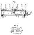
- Fig. 1shows an example of a metallic, but relatively poorly heat-conductive housing 1, 4, 5, 6, which a bottom pan 1, 4 with bottom 1 and side walls 4, and one - preferably hermetically sealed - attached to the bottom pan 1, 4
- Outer cover 5, 6 with outer cover plate 5 and - for example screwed onto the outer cover plate 5 -includes cooling fin part 6.
- An electrical circuit component 11, 17 which emits heat loss during operationis mounted in the housing, which in turn is e.g. is formed by an infrared light-emitting diode 17 and an upstream semiconductor driver chip 11, that is to say here by two separate components 11, 17.
- the circuit component 11, 17serves in the example shown as an optoelectronic converter of an optoelectronic communication system, in which the circuit component 11, 17 or its structures 11, 17 fastened here on the floor 1 are to be operated close to the then permissible operating temperature and carefully for this purpose by very targeted Measures to be cooled.
- the housingalso contains the electrical supply lines, of which the figure symbolically represents only one line 12 between the two structures 11, 17 and the two supply lines, each of which is insulated from the metallic base 1 by means of glass, namely 15 to the driver chip 11 and 16 to the diode 17 shows.
- the housingalso contains the end of a glass fiber 20 with its glass fiber connection 3 for the light transmission.
- the circuit component 11, 17,which essentially consists of the two structures 11, 17, is - here each structure 11, 17 for itself - attached to the bottom 1 of the base trough 1, 4.
- the heat lossshould largely be given off via the heat-conducting outer cover 5, 6 as heat-conducting body 5, 6 to the outer cover outer surface, and from there to the cooling air flowing around the housing.
- the floor pan 1, 4 of this exampleconsists of relatively poorly heat-conducting material, so that normally the dissipation of the heat loss from the circuit component, here from its two structures 11, 17, would be too bad for the cooling air, especially if at least one of the two structures 11 or 17 already exists should be operated close to its maximum permissible operating temperature.
- the floor panis e.g. made of stainless steel with a thermal conductivity of e.g. only 15 W / m.K or made of FeNi or FeNiCo alloys (Vacodil or Vacon) from e.g. between 10 to 16.7 W / m.K.
- the inventionrelates to another, further possible measure.
- a good heat-conducting liner sheet 2for example made of copper of 385 W / mK, lined
- this liner sheet 2each one has a good heat-conducting transition section both towards the circuit component 11, 17 and towards the heat dissipation body 5, 6.
- the lining sheetitself also has a trough shape, furthermore, for example, cutouts, for example for supply lines 15, 16, and also a flat edge at the top towards the outer cover 5, 6, which can serve as a flat contact surface, cf. Fig. 1.
- Such on Construction of the housingalso generates a high heat capacity close to the circuit component, requires little effort and is therefore suitable for mass production, especially if the lining sheet 2 is inserted into the bottom wall 1, 4 as a separate, prefabricated housing component.
- copper and stainless steeladvantageously have very similar linear coefficients of thermal expansion (Cu 17.7.10 ⁇ 6K ⁇ 1 and CrNi steel, for example 16.10 ⁇ 6K ⁇ s1), so that the lining sheet 7 over very large temperature ranges, for example -40 ° ... . + 125 ° C remains firmly in the floor pan 1.4.
- the two transition sectionscan each be constructed differently.
- a construction of the housing, in which cf. 1, the circuit component, here the driver chip 11,is attached directly to a liner section, which itself represents the transition section, this liner section lying between the circuit component 11 and the base 1.
- a particularly low heat transfer resistance and particularly large tolerances of the dimensionsare achievable for the components in the transition section to the heat dissipation body 5, 6 formed by the outer cover 5, 6 in that surfaces of the lining sheet 2 near the cover, cf. Fig. 1, the contact surface for a good heat conduction form the inner cover 7, the inner cover 7 and a spring body 8, 9, 18, 19 forming a transition section by a highly elastic, good heat-conducting spring body 8, 9, 18, 19 attached between the inner cover 7 and the inner surface of the outer cover 5, 6 is.
- the inner cover 7is preferably made of highly elastic material, e.g. Made of a CuNiBe alloy so that it rests on the lining sheet 2 over as large an area as possible, i.e. with a low heat transfer resistance.
- the spring bodycf. Fig. 1, can be manufactured differently.
- ithas the shape of a corrugated sheet 8, which consists of a good heat-conducting spring sheet, e.g. made of a CuNiBe alloy with e.g. 230 W / m.K thermal conductivity.
- the spring bodyhas an even lower thermal resistance if it consists of a spring plate 18, cf. 1 and 2, in which particularly elastic feather tongues 19 are punched with respect to bending and torsion, which nestle well against their bearing surface - on the inner surface of the outer cover plate 5, or if necessary also on the relevant surface of the inner cover 7 - with high contact pressure.
- This feather-tongue spring plate 18, 19can also be produced from highly elastic, highly elastic CuNiBe alloy.
- the spring bodycan also consist of a felt 9 made of metal threads, for example of Cu threads, such felts being easy to cut to the desired size and being easy to insert into the housing.
- the circuit componentconsists of several structures to be shielded from one another at high frequency, cf. 11 and 17 in Fig. 1, then you can insert into the lining sheet 2, an intermediate wall 10 made of a good heat-conducting material to form a plurality of electrically shielded chambers in the interior of the housing, such an inserted intermediate wall 10 in addition to heat dissipation between the floor of the lining sheet 2 and the outer cover 5, 6 - or inner cover 7 - can also be used.
- the housingcontains several components as a circuit component
- several different lining sheetscan also be attached in the housing, which are each connected to a part of the components in a heat-conducting manner and which are each connected to their own housing surfaces via their own heat-conducting bodies . It is then possible for the individual lining sheets to have different temperatures from one another, as a result of which the operating temperatures of the individual structures can also be selected differently.
- This attachment of several liner sheets, which are then not connected to one another with good thermal conductivity,is particularly favorable if each of the structures is to be operated independently up to its maximum permissible operating temperature, although all these structures and all of their liner sheets are mounted in the same, single housing.
Landscapes
- Physics & Mathematics (AREA)
- General Physics & Mathematics (AREA)
- Optics & Photonics (AREA)
- Engineering & Computer Science (AREA)
- Microelectronics & Electronic Packaging (AREA)
- Condensed Matter Physics & Semiconductors (AREA)
- Computer Hardware Design (AREA)
- Power Engineering (AREA)
- Cooling Or The Like Of Electrical Apparatus (AREA)
Abstract
Translated fromGermanDescription
Translated fromGermanDie Erfindung geht von einem speziellen, im Oberbegriff des Patentanspruchs 1 definierten Gehäuse aus, welches für sich z.B. aus der DE-OS 33 37 131 vorbekannt ist.The invention is based on a special housing defined in the preamble of claim 1, which for example is already known from DE-OS 33 37 131.
Die Erfindung hat die Aufgabe, mit möglichst wenig Aufwand die Kühlung des am Boden im Gehäuse-Inneren angebrachten Schaltungsbauteiles dann zu verbessern, wenn große Teile des Gehäuses, z.B. die ganze Bodenwanne, zu schlecht wärmeleitend sind, um im Betrieb die Verlustwärme, zumindest einen hohen Anteil davon, des Schaltungsbauteiles, an das umströmende Kühlmedium abzuleiten. Dabei kann das Verlustwärme abgebende Schaltungsbauteil selber aus mehreren diskret im Gehäuse angebrachten Baukörpern bestehen, also z.B. aus einer 1W Verlustleistung aufweisenden Lichtsendediode sowie einen dazugehörenden, selber auch eine ähnlich hohe Verlustleistung aufweisenden Treiber-Chip als Hochfrequenz-Vorverstärker der Lichtsendediode. Zum sicheren Betrieb eines solchen Schaltungsteiles müssen die beiden Baukörper ausreichend gekühlt werden, was bei, insgesamt gesehen, zu schlecht wärmeleitenden Materialien für große Teile des Gehäuses erhebliche Schwierigkeiten macht, z.B. bei aus Korrosionsschutzgründen gewähltem Edelstahl für den Boden oder für die ganze Bodenwanne - ganz besonders wenn eine große Vielzahl solcher Gehäuse dicht gepackt eng nebeneinander auf einer Platte befestigt werden, so daß die Kühlung im wesentlichen nur über den Außendeckel möglich ist. Außerdem sollen die erfindungsgemäßen Maßnahmen auch sine beachtliche Wärmekapazität nahe genug beim Schaltungsbauteil erzeugen, um kurzzeitige sehr hohe Verlustleistungsspitzen aufzufangen.The object of the invention is to improve, with as little effort as possible, the cooling of the circuit component attached to the floor inside the housing when large parts of the housing, for example the entire floor pan, are too poorly heat-conducting to dissipate the heat, at least a high one, during operation Share of it, the circuit component, to the cooling medium flowing around. The circuit component that emits heat loss can itself consist of a number of structures discreetly mounted in the housing, for example, a light emitting diode with 1W power loss and an associated driver chip, which itself has a similarly high power loss, as a high-frequency preamplifier for the light emitting diode. For the safe operation of such a circuit part, the two structures must be adequately cooled, which, viewed overall, makes materials with poor thermal conductivity for large parts of the housing considerable difficulties, for example with stainless steel chosen for corrosion protection reasons for the floor or for the entire floor pan - especially if a large number of such housings are packed tightly next to each other on a plate, so that cooling is essentially only possible via the outer cover. In addition, the measures according to the invention should also generate their considerable heat capacity close enough to the circuit component in order to absorb short-term, very high power loss peaks.
Diese Aufgabe wird erfindungsgemäß durch die im Patentanspruch 1 angegebenen Maßnahmen gelöst.This object is achieved by the measures specified in claim 1.
Die in den Unteransprüchen angegebenen zusätzlichen Maßnahmen gestatten, zusätzliche Vorteile zu erreichen, nämlich die Maßnahmen gemäß Patentanspruch
- 2 und 3, einen besonders niedrigen Aufwand aufbringen zu müssen;
- 4, unter erschwerten Voraussetzungen einen niedrigen Wärmeübergangswiderstand zwischen dem Schaltungsbauteil - oder einem Baukörper davon - einerseits und dem - bevorzugt Bodenbereich vom - Auskleidungsblech andererseits erreichen zu können;
- 5, selbst bei Massenfertigung mit besonders wenig Aufwand, trotz großer Herstellungstoleranzen eines Innendeckels, einen kleinen Wärmeübergangswinderstand zwischen dem Auskleidungsblech und dem Außendeckel erreichen zu können;
- 6, Zwischenwände gleichzeitig sowohl zur Verbesserung der Kühlung als auch zur Abschirmung zwischen verschliedenen Baukörpern des Schaltungsbauteils ausnutzen zu können, sowie
- 7, den Wärmeübergangswiderstand zwischen dem Auskleidungsblech und den Außendeckel sehr kelein machen zu können, ohne enge Herstellungstoleranze für das Auskleidungsblech und den Außendeckel einhalten zu müssen.
- 2 and 3, to have to spend a particularly low effort;
- 4, under difficult conditions, to be able to achieve a low heat transfer resistance between the circuit component - or a structure thereof - on the one hand and the - preferably bottom area of - the liner sheet;
- 5, even with mass production with particularly little effort, despite large manufacturing tolerances of an inner cover, to be able to achieve a small heat transfer resistance between the lining sheet and the outer cover;
- 6, to be able to utilize partition walls at the same time both for improving the cooling and for shielding between different components of the circuit component, and
- 7, to be able to make the heat transfer resistance between the lining sheet and the outer cover very small, without having to adhere to tight manufacturing tolerances for the lining sheet and the outer cover.
Die Erfindung und ihre Weiterbildungen werden anhand der beiden Figuren weiter erläutert, wobei die Figur
- 1 einen senkrechten Schnitt durch ein von der Seite betrachtetes , einen optoelektronischen Wandler enthaltendes Gehäusebeispiel der Erfindung, und
- 2 vergrößert ein Detail einer Weiterbildung in Draufsicht
- 1 shows a vertical section through a housing example of the invention, viewed from the side and containing an optoelectronic converter, and
- 2 enlarges a detail of a further development in plan view
Die Fig. 1 zeigt ein Beispiel eines metallischen, aber relativ schlecht wärmeleitenden Gehäuses 1, 4, 5, 6 , welches eine Bodenwanne 1, 4 mit Boden 1 und Seitenwänden 4, sowie einen - bevorzugt hermetisch dicht - auf der Bodenwanne 1, 4 befestigten Außendeckel 5, 6 mit Außendeckelplatte 5 und - z.B. auf die Außendeckelplatte 5 geschraubtem - Kühlrippenteil 6 enthält. Im Gehäuse ist ein elektrisches, im Betrieb Verlustwärme abgebendes Schaltungsbauteil 11, 17 angebracht, welches seinerseits z.B. durch eine Infrarot-Lichtsendediode 17 und einen vorgeschaltetem Halbleiter-Treiber-Chip 11, also hier durch zwei getrennte Baukörper 11, 17 gebildet wird. Das Schaltungsbauteil 11, 17 dient im gezeigten Beispiel nämlich als optoelektronischer Wandler eines optoelektronischen Kommunikationssystems, bei welchem das Schaltungsbauteil 11, 17 bzw. seine hier am Boden 1 befestigten Baukörper 11, 17 nahe der dann höchstzulässigen Betriebstemperatur betrieben werden sollen und dazu sorgfältig durch sehr gezielte Maßnahmen zu kühlen sind.Fig. 1 shows an example of a metallic, but relatively poorly heat-
Das Gehäuse enthält ferner die elektrischen Versorgungsleitungen, von denen die Figur symbolisch nur eine Leitung 12 zwischen den beiden Baukörpern 11, 17 sowie die beiden jeweils mittels Glas gegen den metallischen Boden 1 isolierten Zuleitungen, nämlich 15 zum Treiber-Chip 11 sowie 16 zur Diode 17 zeigt. Das Gehäuse enthält ferner das Ende einer Glasfaser 20 mit deren Glasfaseranschluß 3 für die Lichtweiterleitung.The housing also contains the electrical supply lines, of which the figure symbolically represents only one line 12 between the two
Das hier im wesentlichen aus den beiden Baukörpern 11, 17 bestehende Schaltungsbauteil 11, 17 ist - hier jeder Baukörper 11, 17 für sich - am Boden 1 der Bodenwanne 1, 4 befestigt. Die Verlustwärme soll weitgehend über den gut wärmeleitenden Außendeckel 5, 6 als Wärmeleitkörper 5, 6 an die Außendeckel-Außenoberfläche, und von dort weiter an die das Gehäuse umströmende Kühlluft abgegeben werden.The
Die Bodenwanne 1, 4 dieses Beispiels besteht aus relativ schlecht wärmeleitendem Material, so daß normalerweise die Ableitung der Verlustwärme vom Schaltungsbauteil, hier von dessen zwei Baukörpern 11, 17, zur Kühlluft zu schlecht wäre, besonders wenn zumindest einer der beiden Baukörper 11 oder 17 bereits nahe bei seiner höchstzulässigen Betriebstemperatur betrieben werden soll. Die Bodenwanne besteht also z.B. aus Edelstahl mit einer Wärmeleitfähigkeit von z.B. nur 15 W/m.K oder aus FeNi- oder FeNiCo-Legierungen (Vacodil oder Vacon) von z.B. zwischen 10 bis 16,7 W/m.K.The floor pan 1, 4 of this example consists of relatively poorly heat-conducting material, so that normally the dissipation of the heat loss from the circuit component, here from its two
An sich kann man zur Verbesserung der Wärmeableitung zusätzlich auch sonstige nicht im vorleigender Hauptanspruch genannte Maßnahmen durchführen, z.B. jene in den älteren, nicht vorveröffentlichten Europäischen Anmeldungen 85 10 9825.1 (VPA 84 P 1584 E) und 85 10 9827.7 (VPA 84 P 1583 E) beschriebenen Maßnahmen sowie die Maßnahmen, welche in der prioritätsgleichen, mit der vorliegenden Anmeldung einereichten Deutschen Anmeldung P .. .. ..... (VPA 85 E 1747 DE = VPA 85 P 1588 DE) beschrieben sind.As such, in order to improve heat dissipation, other measures not mentioned in the previous main claim can also be carried out, e.g. those measures described in the older, not prepublished European applications 85 10 9825.1 (VPA 84 P 1584 E) and 85 10 9827.7 (VPA 84 P 1583 E) as well as the measures described in the priority German application P. ... .. (VPA 85 E 1747 DE = VPA 85 P 1588 DE).
Die Erfindung betrifft eine andere, weitere mögliche Maßnahme. Gemäß der Erfindung wird nämlich, vgl. Fig. 1, zumindest ein Teil sowohl der Innenoberfläche des Bodens 1 als auch der Bodenwanne-Seitenwände 4 der Bodenwanne 1, 4 mit einem gut wärmeleitendem Auskleidungsblech 2, z.B. aus Kupfer von z.B. 385 W/m.K, ausgekleidet, wobei dieses Ausksleidungsblech 2 jeweils einen gut wärmeleitenden Übergangsabschnitt sowohl zum Schaltungsbauteil 11, 17 hin als auch einen zum Wärmeableitkörper 5, 6 hin aufweist. Bevorzugterweise hat das Auskleidungsblech selbst auch eine Wannenform, ferner z.B. Aussparungen, z.B. für Zuleitungen 15, 16, sowie oben zum Außendeckel 5, 6 hin einen ebenen Rand, der als ebene Auflagefläche dienen kann, vgl. Fig. 1. Ein solcher Auf bau des Gehäuses erzeugt auch eine hohe Wärmekapazität nahe beim Schaltungsbauteil, benötigt zuden wenig Aufwand und ist daher für die Massenfertigung geeignet, ganz besonders dann, wenn zusätzlich das Auskleidungsblech 2 als eigener massiver vorgefertigter Gehäusebestandteil in die Bodenwannd 1, 4 gesteckt ist. Vorteilhafterweise haben übrigens Kupfer und Edelstahl sehr ähnliche linear Wärmeausdehungs-Koeffizienten (Cu 17,7.10⁻⁶K⁻¹ und CrNi-Stahl z.B. 16.10⁻⁶K⁻s1), so daß das Auskleidungsblech 7 über sehr große Temperaturbereiche, z.B. -40° ....+125°C gleichbleibend fest in der Bodenwanne 1,4 haftet.The invention relates to another, further possible measure. According to the invention, namely, cf. Fig. 1, at least a part of both the inner surface of the floor 1 and the floor pan side walls 4 of the floor pan 1, 4 with a good heat-conducting liner sheet 2, for example made of copper of 385 W / mK, lined, this liner sheet 2 each one has a good heat-conducting transition section both towards the
Die beiden Übergangsabschnitte können jeweils verschieden aufgebaut werden. Besonders günstig und aufwandsarm erwies sich ein Aufbau des Gehäuses, bei welchem vgl. Fig. 1, das Schaltungsbauteil, hier der Treiber-Chip 11 direkt auf einem Auskleidungsblech-Abschnitt, welcher selbst den Übergangsabschnitt darstellt, befestigt ist, wobei dieser Auskleidungsblech-Abschnitt zwischen dem Schaltungsbauteil 11 und dem Boden 1 liegt.The two transition sections can each be constructed differently. A construction of the housing, in which cf. 1, the circuit component, here the
Man kann jedoch auch bei Bedarf, vgl. Fig. 1, auch zwischen dem Schaltungsbauteil, hier der Lichtsendediode,und dem Auskleidungsblech 2 eine gut wärmeleitende, massive. Wärmeleitbrücke 13, 14 als Übergangsabschnitt einfügen, -wobei diese Wärmeleitbrücke, vgl. 13,zusätzlich als Sockel für das betreffende Schaltungsbauteil/Baukörper 11 dienen kann, oder als wärmeableitende seitliche Lasche oder Stütze 14.However, if necessary, cf. Fig. 1, also between the circuit component, here the light emitting diode, and the lining sheet 2 a good heat-conductive, massive. Insert
Einen besonders niedrigen Wärmeübergangswiderstand und besonders große Toleranzen der Maß sind für die Bauteile im Übergangsbschnitt zum durch den Außendeckel 5, 6 gebildeten Wärmeableitkörper 5, 6 dadurch erreichbar, daß deckelnahe Oberflächen des Auskleidungsbleches 2, vgl. Fig. 1, die Auflagefläche für einen gut wärmeleiten den Innendeckel 7 bilden, wobei der Innendeckel 7 und ein Federkörper 8, 9, 18, 19 einen Übergangsabschnitt bilden, indem zwischen dem Innendeckel 7 und der Innenoberfläche des Außendeckels 5, 6 ein hochelastischer, gut wärmeleitender Federkörper 8, 9, 18, 19 angebracht ist.A particularly low heat transfer resistance and particularly large tolerances of the dimensions are achievable for the components in the transition section to the
Der Innendeckel 7 besteht bevorzugt aus hochelastischem Material, z.B. aus einer CuNiBe-Legierung, damit er möglichst großflächig, also mit niedrigem Wärmeübergangswiderstand, auf dem Auskleidungsblech 2 aufliegt.The
Der Federkörper, vgl. Fig. 1, kann hierbei verschieden hergestellt werder. Z.B. hat er die Form eines Wellbleches 8, das aus gut wärmeleitendem Federblech besteht, z.B. aus einer CuNiBe-Legierung mit z.B. 230 W/m.K Wärmeleitfähigkeit.The spring body, cf. Fig. 1, can be manufactured differently. E.g. it has the shape of a corrugated sheet 8, which consists of a good heat-conducting spring sheet, e.g. made of a CuNiBe alloy with e.g. 230 W / m.K thermal conductivity.
Der Federkörper hat einen noch niedrigeren Wärmewiderstand, wenn er aus einem Federblech 18 besteht, vgl. Fig. 1 und 2, in welches hinsichtlich Beigung und Torsion besonders elastische Fiederzungen 19 gestanzt sind, die sich gut an ihre Auflagefläche - an der Innenoberfläche der Außendeckelplatte 5, oder bei Bedarf auch an die betreffende Oberfläche des Innendeckels 7 - mit hohem Auflagedruck anschmiegen. Auch dieses Fiederzungen-Federblech 18, 19 kann aus sehr gut wärmeleitenden hochelastischen CuNiBe-Legierung hergestellt werden.The spring body has an even lower thermal resistance if it consists of a
Der Federkörper kann auch aus einem Filz 9 aus Metallfäden, z.B. aus Cu-Fäden bestehen, wobei solche Filze leicht auf das gewünschte Maß zu schneiden und leicht in die Gehäuse einlegbar sind.The spring body can also consist of a felt 9 made of metal threads, for example of Cu threads, such felts being easy to cut to the desired size and being easy to insert into the housing.
Wenn das Schaltungsbauteil aus mehreren, voneinander hochfrequenzmäßig abzuschirmenden Baukörpern besteht, vgl. 11 und 17 in Fig. 1, dann kann man in das Auskleidungsblech 2 eine aus gut wärmeleitendem Material bestehende Zwischenwand 10 zur Bildung von mehreren, voneinander elektrisch abgeschirmten Kammern im Gehäuse-Inneren einfügen, wobei eine so eingefügte Zwischenwand 10 zusätzlich zur Wärmeableitung zwischen dem Boden des Auskleidungsbleches 2 und dem Außendeckel 5, 6 - bzw. Innendeckel 7 - mitausgenutzt werden kann.If the circuit component consists of several structures to be shielded from one another at high frequency, cf. 11 and 17 in Fig. 1, then you can insert into the lining sheet 2, an
Wenn, wie im gezeigten Beispiel, das Gehäuse mehrere Baukörper als Schaltungsbauteil enthält, können auch mehrere verschiedene Auskleidungsbleche im Gehäuse angebracht werden, welche jeweils mit einem Teil der Baukörper wärmeleitend verbunden werden und welche jeweils über eigene Wärmeleitkörper zu eigenen Gehäuse-Oberflächen hin wärmeleitend verbunden sind. Dann ist es möglich, daß die einzelnen Auskleidungsbleche untereinander verschiedene Temperaturen aufweisen, wodurch auch die Betriebstemperaturen der einzelnen Baukörper verschieden gewählt werden können. Diese Anbringung mehrerer, dann untereinander nicht gut wärmeleitend verbundener Auskleidungsbleche ist also besonders günstig, wenn jeder der Baukörper für sich jeweils bis nahe seiner höchstzulässigen Betriebstemperatur betrieben werden soll, obwohl alle diese Baukörper und alle ihre Auskleidungsbleche im selben, einzigen Gehäuse angebracht sind.If, as in the example shown, the housing contains several components as a circuit component, several different lining sheets can also be attached in the housing, which are each connected to a part of the components in a heat-conducting manner and which are each connected to their own housing surfaces via their own heat-conducting bodies . It is then possible for the individual lining sheets to have different temperatures from one another, as a result of which the operating temperatures of the individual structures can also be selected differently. This attachment of several liner sheets, which are then not connected to one another with good thermal conductivity, is particularly favorable if each of the structures is to be operated independently up to its maximum permissible operating temperature, although all these structures and all of their liner sheets are mounted in the same, single housing.
- 1 Boden der Bodenwanne1 bottom of the floor pan
- 2 Auskleidungsblech2 lining sheet
- 3 Glasfaseranschluß3 fiber optic connection
- 4 Seitenwand der Bodenwanne4 side wall of the floor pan
- 5 Außendeckel / Wärmeableitkörper5 outer cover / heat sink
- 6 Außendeckel / Wärmeableitkörper6 outer cover / heat sink
- 7 Innendeckel7 inner cover
- 8 Federkörper8 spring bodies
- 9 Federkörper9 spring body
- 10 Zwischenwand10 partition
- 11 Schaltungsbauteil / Treiber-Chip11 Circuit component / driver chip
- 12 Versorgungsleitung12 supply line
- 13 Wärmeleitbrücke13 thermal bridge
- 14 Wärmeleitbrücke14 thermal bridge
- 15 Versorgungsleitung15 supply line
- 16 Versorgungsleitung16 supply line
- 17 Schaltungsbauteil / Infrarot-Lichtsendediode17 circuit component / infrared light-emitting diode
- 18 Ferderkörper18 spring body
- 19 Federkörper / Fiederzungen19 spring body / tongues
- 20 Glasfaser20 glass fiber
Claims (8)
Translated fromGerman- das Schaltungsbauteil(11, 17) am Boden(1) der Bodenwanne (1, 4) befestigt ist, und
- die Verlustwärme zumindest zu einem erheblichen Teil über einen Wärmeableitkörper(5, 6) des Gehäuses(1, 4, 5, 6) an eine Gehäuse-Abßenoberfläche, bevorzugt über den gut wärmeleitenden Außendeckel(5, 6) als Wärmeableitkörper(5, 6) an die Außendeckel(6)-Außenoberfläche, und von dort weiter an ein das Gehäuse umströmendes Kühlmedium, bovorzugt Kühlluft, abzugeben ist,
z.B. für einen elektrisch-optischen Wandler eines optoelektronischen Kommunikationssystems mit einem Schaltungsbauteil(11, 17), welches gleichzeitig sowohl eine gut zu kühlende Infrarot-Lichtsendediode(17) als auch einen gut zu kühlenden Treiber-Chip(11) sowie elektrische Versorgungsleitungen(12, 15, 16) enthält, und mit einen Glasfaseranschluß(3, 20) zur Lichtweiterleitung,
dadurch gekennzeichnet, daß
- zumindest ein Teil sowohl der Boden(1)-Innenoberfläche als auch der Bodenwanne-Seitenwände(4) der, insgesamt gesehen, relativ schlecht wärmeleitenden Bodenwanne(1, 4) mit einem gut wärmeleitenden Auskleidungsblech(2) ausgekleidet ist, und
- das Auskleidungsblech(2) jeweils einen gut wärmeleitenden Übergangsabschnitt sowohl zum Schaltungsbauteil(11, 17) hin als auch einen zum Wärmeableitkörper(5, 6) hin aufweist.1. Housing (1, 4, 5, 6) with a floor pan (1, 4) and with an outer cover (5, 6), preferably hermetically sealed, on the floor pan (1, 4) for an electrical heat loss during operation emitting circuit component (11, 17), for example for a light emitting diode (17) and / or for a semiconductor chip (11), wherein
- The circuit component (11, 17) on the bottom (1) of the floor pan (1, 4) is attached, and
- The heat loss at least to a considerable extent via a heat sink (5, 6) of the housing (1, 4, 5, 6) to a housing outer surface, preferably via the heat-conducting outer cover (5, 6) as a heat sink (5, 6 ) to the outer cover (6) outer surface, and from there to a cooling medium flowing around the housing, preferably cooling air,
eg for an electrical-optical converter of an optoelectronic communication system with a circuit component (11, 17), which at the same time has both an infrared light-emitting diode (17) that is easy to cool and a driver chip (11) that is easy to cool as well as electrical supply lines (12, 15, 16), and with a glass fiber connection (3, 20) for light transmission,
characterized in that
- At least part of both the floor (1) inner surface and the floor pan side walls (4) of the overall, relatively poorly heat-conducting floor pan (1, 4) is lined with a good heat-conducting lining sheet (2), and
- The lining sheet (2) each has a good heat-conducting transition section both towards the circuit component (11, 17) and towards the heat dissipation body (5, 6).
dadurch gekennzeichnet , daß
- das Auskleidungsblech(2) als eigener massiver Gehäusebestandteil in die Bodenwanne(1, 4) gesteckt ist.
(Fig.1)2. Housing according to claim 1,
characterized in that
- The lining sheet (2) is inserted as a separate solid housing component in the floor pan (1, 4).
(Fig.1)
dadurch gekennzeichnet , daß
- das Schaltungsbauteil(11) direkt auf einem Auskleidungsblech(2)-Abschnitt, welcher selbst einen Übergangsabschnitt darstellt, befestigt ist, und
- der Auskleidungsblech(2)-Abschnitt zwischen dem Schaltungsbauteil(11) und dem Boden(1) liegt.
(Fig.1)3. Housing according to claim 1 or 2,
characterized in that
- The circuit component (11) directly on a lining sheet (2) section, which itself is a transition section, is attached, and
- The lining sheet (2) section between the circuit component (11) and the bottom (1).
(Fig.1)
dadurch gekennzeichnet , daß
- zwischen dem Schaltungsbauteil(17) und dem Auskleidungsblech (2)eine gut wärmeleitende, massive Wärmeleitbrücke(13, 14) als Übergangsabschnitt eingefügt ist.
(Fig.1)4. Housing according to one of the preceding claims,
characterized in that
- Between the circuit component (17) and the lining sheet (2) a good heat-conducting, massive thermal bridge (13, 14) is inserted as a transition section.
(Fig.1)
dadurch gekennzeichnet , daß
- deckelnahe Oberflächen des Auskleidungsbleches(2) die Auflagefläche für einen gut wärmeleitenden Innendeckel (7) bilden, und
- der Innendeckel(7) und ein Federkörper(8, 9, 18, 19) einen Übergangsabschnitt bilden, indem
- - zwischen dem Innendeckel(7) und der Innenoberfläche des einen Wärmeableitkörper bildenden Außendeckels(5, 6) ein hochelastischer, gut wärmeleitender Federkörper(8, 9, 18, 19) angebrach ist.
(Fig.1)5. Housing according to one of the preceding claims,
characterized in that
- Close surfaces of the lining sheet (2) form the support surface for a good heat-conducting inner cover (7), and
- The inner cover (7) and a spring body (8, 9, 18, 19) form a transition section by
- - Between the inner cover (7) and the inner surface of the outer cover forming a heat dissipation body (5, 6) a highly elastic, good heat-conducting spring body (8, 9, 18, 19) is attached.
(Fig.1)
dadurch gekennzeichnet , daß
- der Federkörper(18, 19) ausgestanzt aber noch an ihm hängend Fiederzungen (19) aufweist
(Fig.1+2)6. Housing according to claim 5,
characterized in that
- The spring body (18, 19) punched out but still has tongues (19) hanging on it
(Fig. 1 + 2)
dadurch gekennzeichnet , daß
- das Auskleidungsblech(2) zumindest eine aus gut wärmeleitendem Material bestehende Zwischenwand(10) zur Bildung von mehreren, voneinander elektrisch abgeschirmten Kammern im Gehäuse-Inneren aufweist.
(Fig.1)7. Housing according to one of the preceding claims,
characterized in that
- The lining sheet (2) has at least one intermediate wall (10) made of a good heat-conducting material to form several chambers that are electrically shielded from one another in the interior of the housing.
(Fig.1)
dadurch gekennzeichnet , daß
- mehrere Wärmeauskleidbleche(2), welche schlecht wärmeleitend miteinander verbunden sind, angebracht sind, - jedes Auskleidungsblech(2) jeweils nur mit eigenen Baukörpern(11) des Schaltungsbauteils(11, 17) gut wärmeleitend verbunden sind,
- die mit verschiedenen Auskleidungsblechen gut wärmeleitend verbundenen Baukörper(11, 17) untereinander schlecht wärmeleitend verbunden sind, und
- jedes der Auskleidungsbleche mit eigenen Gehäuse-Außenoberflächen gut wärmeleitend verbunden sind.8. Housing according to one of the preceding claims,
characterized in that
- A plurality of heat-liner sheets (2), which are connected to one another with poor thermal conductivity, are attached, - Each liner sheet (2) is only connected with good heat-conducting properties with its own structures (11) in the circuit component (11, 17),
- The structures (11, 17) connected to each other with poorly conductive conductors with different lining sheets, and
- Each of the lining sheets are connected with their own outer housing surfaces with good thermal conductivity.
Applications Claiming Priority (2)
| Application Number | Priority Date | Filing Date | Title |
|---|---|---|---|
| DE3531135 | 1985-08-30 | ||
| DE3531135 | 1985-08-30 |
Publications (1)
| Publication Number | Publication Date |
|---|---|
| EP0213426A1true EP0213426A1 (en) | 1987-03-11 |
Family
ID=6279824
Family Applications (1)
| Application Number | Title | Priority Date | Filing Date |
|---|---|---|---|
| EP86110758AWithdrawnEP0213426A1 (en) | 1985-08-30 | 1986-08-04 | Casing with a lower and an upper cap for an electrical circuit element |
Country Status (2)
| Country | Link |
|---|---|
| US (1) | US4763225A (en) |
| EP (1) | EP0213426A1 (en) |
Cited By (6)
| Publication number | Priority date | Publication date | Assignee | Title |
|---|---|---|---|---|
| EP0308748A3 (en)* | 1987-09-25 | 1990-07-04 | Siemens Aktiengesellschaft | Electrooptical unit |
| EP0308749A3 (en)* | 1987-09-25 | 1990-07-11 | Siemens Aktiengesellschaft | Electrooptical unit |
| US5436997A (en)* | 1992-10-14 | 1995-07-25 | Fujitsu Limited | Optical fiber-optical device coupling package and optical fiber-optical device module |
| WO2000004588A1 (en)* | 1998-07-14 | 2000-01-27 | Infineon Technologies Ag | Electrooptical assembly group |
| WO2011120188A1 (en) | 2010-03-29 | 2011-10-06 | Telefonaktiebolaget L M Ericsson (Publ) | Cooling device for pluggable module, assembly of the cooling device and the pluggable module |
| CN110750026A (en)* | 2019-09-25 | 2020-02-04 | 深圳市火乐科技发展有限公司 | Projector with a light source |
Families Citing this family (49)
| Publication number | Priority date | Publication date | Assignee | Title |
|---|---|---|---|---|
| DE3738506A1 (en)* | 1987-11-13 | 1989-06-01 | Dornier System Gmbh | ANTENNA STRUCTURE |
| US4899256A (en)* | 1988-06-01 | 1990-02-06 | Chrysler Motors Corporation | Power module |
| US5357418A (en)* | 1991-05-02 | 1994-10-18 | Robert Clavel | Hybrid power supply for converting an alternating input signal into a direct output signal |
| FR2686213B1 (en)* | 1992-01-14 | 1994-05-06 | Applications Gles Elect Meca | RECEIVER HOUSING FOR ELECTRONIC DISSIPATORS. |
| US6734363B1 (en) | 1992-07-07 | 2004-05-11 | International Business Machines Corporation | Lightweight electronic equipment conductor with coolant permeable support |
| EP0579010A1 (en)* | 1992-07-07 | 1994-01-19 | International Business Machines Corporation | Lightweight packaging |
| JP2570588B2 (en)* | 1993-07-29 | 1997-01-08 | 日本電気株式会社 | Transceiver |
| JP2570605B2 (en)* | 1993-11-15 | 1997-01-08 | 日本電気株式会社 | Semiconductor device |
| US5999406A (en)* | 1995-02-23 | 1999-12-07 | Avid Technology, Inc. | Dockable electronic equipment container |
| US5602718A (en)* | 1995-09-29 | 1997-02-11 | Hewlett-Packard Company | Thermal sink for a transducer assembly |
| US5745344A (en)* | 1995-11-06 | 1998-04-28 | International Business Machines Corporation | Heat dissipation apparatus and method for attaching a heat dissipation apparatus to an electronic device |
| SE512021C2 (en)* | 1997-06-03 | 2000-01-17 | Ericsson Telefon Ab L M | Apparatus and method for cooling and protecting electronics |
| US5892872A (en)* | 1997-07-17 | 1999-04-06 | Northern Telecom Limited | Network unit enclosure |
| JP4121185B2 (en)* | 1998-06-12 | 2008-07-23 | 新電元工業株式会社 | Electronic circuit equipment |
| US6213651B1 (en) | 1999-05-26 | 2001-04-10 | E20 Communications, Inc. | Method and apparatus for vertical board construction of fiber optic transmitters, receivers and transceivers |
| US6901221B1 (en) | 1999-05-27 | 2005-05-31 | Jds Uniphase Corporation | Method and apparatus for improved optical elements for vertical PCB fiber optic modules |
| US6624979B1 (en) | 2000-06-09 | 2003-09-23 | Iomega Corporation | Method and apparatus for parking and releasing a magnetic head |
| US6717762B1 (en) | 2000-06-09 | 2004-04-06 | Iomega Corporation | Method and apparatus for making a drive compatible with a removable cartridge |
| US6628474B1 (en) | 2000-06-09 | 2003-09-30 | Iomega Corporation | Method and apparatus for electrostatic discharge protection in a removable cartridge |
| US6633445B1 (en) | 2000-06-09 | 2003-10-14 | Iomega Corporation | Method and apparatus for electrically coupling components in a removable cartridge |
| FR2816111B1 (en)* | 2000-10-26 | 2003-01-03 | Framatome Connectors Int | OPTOELECTRONIC TRANSCEIVER DEVICE |
| JP2002202441A (en)* | 2000-11-02 | 2002-07-19 | Nippon Telegr & Teleph Corp <Ntt> | Optical active connector plug and connector port for LAN |
| US6781782B2 (en) | 2000-12-21 | 2004-08-24 | Iomega Corporation | Method and apparatus for saving calibration parameters for a removable cartridge |
| US6496362B2 (en) | 2001-05-14 | 2002-12-17 | Iomega Corporation | Method and apparatus for protecting a hard disk drive from shock |
| US6779067B2 (en) | 2001-05-14 | 2004-08-17 | Iomega Corporation | Method and apparatus for providing extended functionality for a bus |
| US6901525B2 (en) | 2001-05-25 | 2005-05-31 | Iomega Corporation | Method and apparatus for managing power consumption on a bus |
| JP3784011B2 (en)* | 2001-07-18 | 2006-06-07 | 本田技研工業株式会社 | Power control unit for electric vehicles |
| US6948861B2 (en) | 2001-08-01 | 2005-09-27 | Siemens Communications, Inc. | Heat sink for an optical module |
| US7017433B2 (en)* | 2001-10-04 | 2006-03-28 | Ssi Technologies, Inc. | Non-contacting sensor multichip module with integral heat-sinks |
| JP2004085971A (en)* | 2002-08-28 | 2004-03-18 | Opnext Japan Inc | Optical transmission module |
| US7204615B2 (en)* | 2003-03-31 | 2007-04-17 | Lumination Llc | LED light with active cooling |
| US7543961B2 (en)* | 2003-03-31 | 2009-06-09 | Lumination Llc | LED light with active cooling |
| US7556406B2 (en)* | 2003-03-31 | 2009-07-07 | Lumination Llc | Led light with active cooling |
| US7190589B2 (en)* | 2004-10-19 | 2007-03-13 | Cinch Connectors, Inc. | Electronic control enclosure |
| US20070023169A1 (en)* | 2005-07-29 | 2007-02-01 | Innovative Fluidics, Inc. | Synthetic jet ejector for augmentation of pumped liquid loop cooling and enhancement of pool and flow boiling |
| US7932535B2 (en)* | 2005-11-02 | 2011-04-26 | Nuventix, Inc. | Synthetic jet cooling system for LED module |
| US7607470B2 (en)* | 2005-11-14 | 2009-10-27 | Nuventix, Inc. | Synthetic jet heat pipe thermal management system |
| US8030886B2 (en) | 2005-12-21 | 2011-10-04 | Nuventix, Inc. | Thermal management of batteries using synthetic jets |
| US8322889B2 (en) | 2006-09-12 | 2012-12-04 | GE Lighting Solutions, LLC | Piezofan and heat sink system for enhanced heat transfer |
| DE102006061943B4 (en)* | 2006-12-29 | 2023-03-30 | Pictiva Displays International Limited | Light Emitting Device |
| US8830695B2 (en)* | 2007-01-25 | 2014-09-09 | Osram Opto Semiconductors Gmbh | Encapsulated electronic device |
| US8459053B2 (en) | 2007-10-08 | 2013-06-11 | Emerson Climate Technologies, Inc. | Variable speed compressor protection system and method |
| TW200919069A (en)* | 2007-10-25 | 2009-05-01 | Asia Optical Co Inc | Optical engine for improving electromagnetic interference |
| JP5152032B2 (en) | 2008-02-22 | 2013-02-27 | 住友電気工業株式会社 | Optical transceiver |
| JP5422147B2 (en)* | 2008-07-08 | 2014-02-19 | 株式会社日立製作所 | Remote copy system and remote copy method |
| US8599575B1 (en)* | 2010-02-03 | 2013-12-03 | DJM Electronics, Inc | Methods, devices, and systems for filtering electromagnetic interference |
| CN113138448B (en)* | 2016-02-05 | 2022-12-13 | 苏州旭创科技有限公司 | Optical module |
| US11206743B2 (en) | 2019-07-25 | 2021-12-21 | Emerson Climate Technolgies, Inc. | Electronics enclosure with heat-transfer element |
| US11234342B2 (en) | 2019-10-15 | 2022-01-25 | Cisco Technology, Inc. | Corrosion preventive heatsink for network device |
Citations (3)
| Publication number | Priority date | Publication date | Assignee | Title |
|---|---|---|---|---|
| US4394679A (en)* | 1980-09-15 | 1983-07-19 | Rca Corporation | Light emitting device with a continuous layer of copper covering the entire header |
| EP0097782A2 (en)* | 1982-06-28 | 1984-01-11 | International Business Machines Corporation | Thermal conduction bridge element for semiconductor device packages |
| EP0111264A2 (en)* | 1982-12-03 | 1984-06-20 | Siemens Aktiengesellschaft | Transmitting or receiving apparatus for opto-electrical communication equipment |
Family Cites Families (6)
| Publication number | Priority date | Publication date | Assignee | Title |
|---|---|---|---|---|
| US3328642A (en)* | 1964-06-08 | 1967-06-27 | Sylvania Electric Prod | Temperature control means utilizing a heat reservoir containing meltable material |
| US4415025A (en)* | 1981-08-10 | 1983-11-15 | International Business Machines Corporation | Thermal conduction element for semiconductor devices |
| DE3337131A1 (en)* | 1983-10-12 | 1985-04-25 | Siemens AG, 1000 Berlin und 8000 München | FIBERGLASS THROUGH A WALL OPENING OF A HOUSING |
| US4612601A (en)* | 1983-11-30 | 1986-09-16 | Nec Corporation | Heat dissipative integrated circuit chip package |
| EP0171051A1 (en)* | 1984-08-08 | 1986-02-12 | Siemens Aktiengesellschaft | Housing for a semiconductor body radiating heat in operation |
| ATE40022T1 (en)* | 1984-08-08 | 1989-01-15 | Siemens Ag | COMMON HOUSING FOR TWO SEMICONDUCTOR BODY. |
- 1986
- 1986-08-04EPEP86110758Apatent/EP0213426A1/ennot_activeWithdrawn
- 1986-08-25USUS06/900,070patent/US4763225A/ennot_activeExpired - Fee Related
Patent Citations (3)
| Publication number | Priority date | Publication date | Assignee | Title |
|---|---|---|---|---|
| US4394679A (en)* | 1980-09-15 | 1983-07-19 | Rca Corporation | Light emitting device with a continuous layer of copper covering the entire header |
| EP0097782A2 (en)* | 1982-06-28 | 1984-01-11 | International Business Machines Corporation | Thermal conduction bridge element for semiconductor device packages |
| EP0111264A2 (en)* | 1982-12-03 | 1984-06-20 | Siemens Aktiengesellschaft | Transmitting or receiving apparatus for opto-electrical communication equipment |
Non-Patent Citations (2)
| Title |
|---|
| IBM TECHNICAL DISCLOSURE BULLETIN, Band 20, Nr. 7, Dezember 1977, Seiten 2635,2636, New York, US; F.A. SHOTT: "Boat thermal enhancement for semiconductor chips and modules"* |
| IBM TECHNICAL DISCLOSURE BULLETIN, Band 23, Nr. 9, Februar 1981, Seiten 4095,4096, New York, US; E.W. KUNKLER et al.: "Module with removable heat transfer members"* |
Cited By (9)
| Publication number | Priority date | Publication date | Assignee | Title |
|---|---|---|---|---|
| EP0308748A3 (en)* | 1987-09-25 | 1990-07-04 | Siemens Aktiengesellschaft | Electrooptical unit |
| EP0308749A3 (en)* | 1987-09-25 | 1990-07-11 | Siemens Aktiengesellschaft | Electrooptical unit |
| US5436997A (en)* | 1992-10-14 | 1995-07-25 | Fujitsu Limited | Optical fiber-optical device coupling package and optical fiber-optical device module |
| EP0596613A3 (en)* | 1992-10-14 | 1997-01-08 | Fujitsu Ltd | Optical fibre coupling modules. |
| WO2000004588A1 (en)* | 1998-07-14 | 2000-01-27 | Infineon Technologies Ag | Electrooptical assembly group |
| WO2011120188A1 (en) | 2010-03-29 | 2011-10-06 | Telefonaktiebolaget L M Ericsson (Publ) | Cooling device for pluggable module, assembly of the cooling device and the pluggable module |
| EP2553770A4 (en)* | 2010-03-29 | 2013-11-13 | Ericsson Telefon Ab L M | Cooling device for pluggable module, assembly of the cooling device and the pluggable module |
| US8879262B2 (en) | 2010-03-29 | 2014-11-04 | Telefonaktiebolaget L M Ericsson (Publ) | Cooling device for pluggable module, assembly of the cooling device and the pluggable module |
| CN110750026A (en)* | 2019-09-25 | 2020-02-04 | 深圳市火乐科技发展有限公司 | Projector with a light source |
Also Published As
| Publication number | Publication date |
|---|---|
| US4763225A (en) | 1988-08-09 |
Similar Documents
| Publication | Publication Date | Title |
|---|---|---|
| EP0213426A1 (en) | Casing with a lower and an upper cap for an electrical circuit element | |
| DE10153887A1 (en) | Magnetic core mounting system | |
| WO1998054735A1 (en) | Device and method for cooling a planar inductor | |
| WO2012013265A2 (en) | Arrangement for cooling electrical components that generate heat, capacitor assembly, and method for producing an arrangement | |
| EP3475978B1 (en) | Heat conductive insulator | |
| DE19518522C2 (en) | Control device for a motor vehicle | |
| EP3823018A1 (en) | Electronic module comprising a pulsating heat pipe | |
| EP1445799A2 (en) | Heat dissipation device for a semiconductor on a printed circuit board | |
| DE102008059320B4 (en) | Electronic device assembly and heat sink for this | |
| DE202020101852U1 (en) | Thermal interface for multiple discrete electronic devices | |
| EP0770861A1 (en) | Probe with laterally projecting header | |
| WO2009033891A2 (en) | Electronic circuit arrangement having a heat sink that is functionally independent of the installed position, and heat sink therefor | |
| EP0216090A1 (en) | Housing for a heat-radiating circuit component in operation | |
| DE102012014011A1 (en) | Electrical appliance for supplying power to e.g. asynchronous motor, has optical coupler connected with power module, in high voltage region, by parallely arranged strip conductors, where strip conductors are arranged in high voltage region | |
| DE19808592C2 (en) | Device for cooling a planar inductance | |
| EP0268081B1 (en) | Cooling device for semiconductor components | |
| EP0652694B1 (en) | Control apparatus for vehicle | |
| EP1733599A2 (en) | Light-emitting diode arrangement and method for the production thereof | |
| EP0986292B1 (en) | Thermal transfer mat for electrical or electronic apparatuses | |
| DE102019116021B4 (en) | Flexible printed circuit board with thermally conductive connection to a heat sink | |
| DE102005026233B4 (en) | Electric power module | |
| DE7505830U (en) | DEVICE FOR HIGH-VOLTAGE-PROOF AND GOOD THERMAL CONDUCTING INSTALLATION OF SEMICONDUCTOR COMPONENTS | |
| WO2012143005A2 (en) | Junction box for solar modules | |
| EP0417643A2 (en) | Electron beam producing device, particularly for an electron gun | |
| DE4105786A1 (en) | Liquid cooled electrical resistance - has track formed on housing that is box shaped and has liquid circulated through it |
Legal Events
| Date | Code | Title | Description |
|---|---|---|---|
| PUAI | Public reference made under article 153(3) epc to a published international application that has entered the european phase | Free format text:ORIGINAL CODE: 0009012 | |
| AK | Designated contracting states | Kind code of ref document:A1 Designated state(s):DE FR GB IT | |
| 17P | Request for examination filed | Effective date:19870407 | |
| 17Q | First examination report despatched | Effective date:19890222 | |
| STAA | Information on the status of an ep patent application or granted ep patent | Free format text:STATUS: THE APPLICATION IS DEEMED TO BE WITHDRAWN | |
| 18D | Application deemed to be withdrawn | Effective date:19900301 | |
| RIN1 | Information on inventor provided before grant (corrected) | Inventor name:RAPP, LOTHAR Inventor name:PRUSSAS, HERBERT, DIPL.-ING. Inventor name:FRENKEL, FERDINAND, DR., DIPL.-PHYS. |