EP0212904A1 - Optical deflector - Google Patents
Optical deflectorDownload PDFInfo
- Publication number
- EP0212904A1 EP0212904A1EP86305998AEP86305998AEP0212904A1EP 0212904 A1EP0212904 A1EP 0212904A1EP 86305998 AEP86305998 AEP 86305998AEP 86305998 AEP86305998 AEP 86305998AEP 0212904 A1EP0212904 A1EP 0212904A1
- Authority
- EP
- European Patent Office
- Prior art keywords
- waveguide
- main path
- substrate
- deflector
- light beam
- Prior art date
- Legal status (The legal status is an assumption and is not a legal conclusion. Google has not performed a legal analysis and makes no representation as to the accuracy of the status listed.)
- Granted
Links
- 230000003287optical effectEffects0.000titleclaimsabstractdescription34
- 239000000758substrateSubstances0.000claimsabstractdescription58
- 230000005693optoelectronicsEffects0.000claimsabstractdescription17
- 230000005684electric fieldEffects0.000claimsabstractdescription12
- 230000005855radiationEffects0.000claimsdescription9
- 239000004065semiconductorSubstances0.000claimsdescription9
- 239000013078crystalSubstances0.000claimsdescription7
- 230000007423decreaseEffects0.000claimsdescription3
- 238000009792diffusion processMethods0.000claimsdescription3
- 239000002184metalSubstances0.000claimsdescription3
- 238000011144upstream manufacturingMethods0.000claimsdescription3
- 239000000463materialSubstances0.000description7
- 238000010276constructionMethods0.000description2
- VRDIULHPQTYCLN-UHFFFAOYSA-NProthionamideChemical compoundCCCC1=CC(C(N)=S)=CC=N1VRDIULHPQTYCLN-UHFFFAOYSA-N0.000description1
- 230000002159abnormal effectEffects0.000description1
- 230000008030eliminationEffects0.000description1
- 238000003379elimination reactionMethods0.000description1
- 238000000034methodMethods0.000description1
- 238000012986modificationMethods0.000description1
- 230000004048modificationEffects0.000description1
- 239000013307optical fiberSubstances0.000description1
- 230000001902propagating effectEffects0.000description1
- 238000010408sweepingMethods0.000description1
Images

Classifications
- G—PHYSICS
- G02—OPTICS
- G02F—OPTICAL DEVICES OR ARRANGEMENTS FOR THE CONTROL OF LIGHT BY MODIFICATION OF THE OPTICAL PROPERTIES OF THE MEDIA OF THE ELEMENTS INVOLVED THEREIN; NON-LINEAR OPTICS; FREQUENCY-CHANGING OF LIGHT; OPTICAL LOGIC ELEMENTS; OPTICAL ANALOGUE/DIGITAL CONVERTERS
- G02F1/00—Devices or arrangements for the control of the intensity, colour, phase, polarisation or direction of light arriving from an independent light source, e.g. switching, gating or modulating; Non-linear optics
- G02F1/29—Devices or arrangements for the control of the intensity, colour, phase, polarisation or direction of light arriving from an independent light source, e.g. switching, gating or modulating; Non-linear optics for the control of the position or the direction of light beams, i.e. deflection
- G02F1/31—Digital deflection, i.e. optical switching
- G02F1/313—Digital deflection, i.e. optical switching in an optical waveguide structure
- G02F1/3137—Digital deflection, i.e. optical switching in an optical waveguide structure with intersecting or branching waveguides, e.g. X-switches and Y-junctions
Definitions
- the present inventionrelates generally to an optical deflector device for deflecting a light beam, and more particularly to a technique for deflecting a light beam due to an electro-optical effect of an electro-optical material, without using mechanical moving parts.
- An optical deflector for deflecting a light beam within a predetermined angular rangeis used in various devices such as a laser-beam printer and a bar code reader.
- a light deflectorKnown as typical examples of such a light deflector are a polygon mirror and a hologram scanner. These deflectors use mechanical moving parts such as a rotary mechanism and a device for driving the rotary mechanism.
- these optical deflector devicestend to be complicated in construction, relatively large-sized, and are not satisfactory in durability.
- an optical deflectorfor deflecting a light beam within a predetermined range of angle, including a substrate having an electro-optical effect, a three-dimensional waveguide formed on one of opposite surfaces of the substrate, to guide waves of the light beam therethrough, and a plurality of deflector electrode means.
- the waveguideincludes a main path, and a plurality of branch paths diverging from the main path at respective branching portions of the waveguide. The branch paths are angled with respect to the main path so as to cover the predetermined range of angle.
- Each of the plurality of deflector electrode meansis disposed at a corresponding one of the branching portions of the three-dimensional waveguide.
- the deflector electrode meansUpon selective application of an electric voltage to each deflector electrode means, the deflector electrode means produces an electric field locally at the corresponding branching portion of the waveguide, and thereby deflect the light beam from the main path into a corresponding one of the plurality of branch paths, due to the electro-optical effect of the substrate.
- the refractive index of a part of the main path at each branching portion of the three-dimensional waveguideis increased when an electric field is locally produced at that branching portion due to an electro-optical effect of the substrate upon selective application of a voltage to the corresponding deflector electrode means. Therefore, the rays of the light beam which propagate through the above-indicated part of the main path are subject to a higher refractive index and are consequently deflected from the main path into the corresponding branch path, whereby the deflected light rays are passed through the branch path which diverges from the main path at a given angle.
- the light beam propagating through the main path of the waveguidecan be deflected into a selected one of the plurality of branch paths, by applying a suitable voltage to the appropriate deflector electrode means.
- the light beammay be deflected within the predetermined range of angle with respect to the main path.
- each deflector electrode meanscomprises a pair of generally elongate electrodes consisting of an inner electrode and an outer electrode.
- the inner electrodeis disposed on the corresponding branching portion of the waveguide so as to extend parallel to the main path and the corresponding branch path.
- the outer electrodeis spaced a predetermined distance from the inner electrode so as to be located outside the waveguide and extend substantially parallel to the inner electrode.
- each of the branch pathsdiverges from the main path at a branch point of the corresponding branching portion, symmetrically with a corresponding portion of the main path, with respect to a centerline which passes the branch point and which is parallel to a direction of propagation of the light beam through the waveguide.
- Each deflector electrode meanscomprises a pair of electrodes which are disposed on opposite sides of the centerline, symmetrically with each other with respect to the centerline, so as to extend between two points upstream and downstream of the branch point, such that a distance between the pair of electrodes decreases in a downstream direction of the waveguide.
- each of the branch pathsdiverges from the main path symmetrically with the corresponding portion of the main path, with respect to the centerline, as described above.
- each deflector electrode meanscomprises a central electrode having a generally triangular shape, and a pair of side electrodes.
- the central electrodeis disposed in alignment with the centerline such that an apex of the central electrode is positioned in the vicinity of the branch point, whereby a width of the central electrode increases in a downstream direction of the waveguide.
- the side electrodesare disposed on opposite sides of the centerline symmetrically with each other with respect to the centerline, so as to sandwich the corresponding branching portion of the waveguide such that a portion of each side electrode on the downstream side of the branch point is spaced from the central electrode, in the direction perpendicular to said direction of propagation of the light beam.
- the three-dimensional waveguidehas a refractive index which increases in a direction toward a centerline thereof, in a plane perpendicular to a direction of propagation of the light beam through the waveguide, so that the waves of the light beam are trapped in directions of thickness and width of the substrate in the plane.
- the substrateconsists of a single crystal of L iN b0 3 ,
- an optical deflectorfor deflecting a light beam within a predetermined range of angle, including a substrate having an electro-optical effect, a semi-conductor laser element fixed at one of opposite ends of the substrate, a condenser portion formed on one of opposite surfaces of the substrate, and a deflector portion.
- the semi-conductor elementis adapted to emit a laser radiation from the above-indicated one end of the substrate so that the radiation propagates along a plane of the substrate.
- the condenser portionis disposed adjacent to the semi-conductor laser element, to condense the laser radiation into parallel rays of laser light.
- the deflector portionincludes a three-dimensional waveguide formed on the above-indicated one of opposite surfaces of the substrate, and a plurality of deflector electrode means.
- the waveguideis formed to guide therethrough the parallel rays of laser light from the condenser.
- the waveguideincludes a main path, and a plurality of branch paths diverging from the main path at respective branching portions of the waveguide. The branch paths are angled with respect to the main path so as to cover the predetermined range of angle.
- Each of the plurality of deflector electrode meansis disposed at a corresponding one of the branching portions of the three-dimensional waveguide.
- Each deflector electrode meansis adapted to produce an electric field locally at the corresponding branching portion of the waveguide, and thereby deflect the light beam from the main path into a corresponding one of the plurality of branch paths, due to the electro-optical effect of the substrate upon selective application of a voltage to each deflector electrode means.
- the condenser portionis formed by diffusion of a metal through a part of the substrate from the above-indicated one of opposite surfaces of the substrate, so as to give the condenser portion a refractive index which increases toward its center in opposite directions perpendicular to a direction of propagation of the parallel rays of laser light.
- the optical deflectorfurther comprises a toroidal lens for converging the laser light emitted selectively from the ends of the main path and the branch paths of the waveguide which are located at the other of the opposite ends of the substrate remote from the semi-conductor laser element.
- a rectangular substrate 10in the form of a translucent plate which is made of an electro-optical material having an electro-optical effect.
- the substrate 10is formed of a single crystal of LiNb0 3 .
- a condenser portion 16disposed adjacent to one of the opposite longutidinal ends of the substrate 10
- a deflector portion 18disposed between the condenser portion 16 and the other longitudinal end of the substrate 10.
- a semi-conductor laser elementin the form of a chip 14 which emits a laser radiation so that the radiation is incident upon the condenser portion 16.
- the condenser portion 16is adapted to function as a convex lens for condensing condense the incident radiation from the laser chip 14 into parallel rays of laser light.
- This condenser portion 16is formed by diffusion of a suitable metal such as Ti through a part of the substrate 10 from the upper major surface, such that the condenser portion 16 has a refractive index which increases toward its center in opposite directions along the width of the substrate 10, i.e., in opposite directions perpendicular to the direction of propagation of the parallel rays of laser light emitted from the condenser portion 16. While the condenser portion 16 cannot be visually distinguished from the substrate 10, its continuously varying refractive index is indicated by parallel straight lines in Fig. 1. The density of the straight lines indicates the refractive index.
- the condenser portion 16may be replaced by a geodesic lens provided in the form of a part-spherical concave cavity formed in the upper major surface of the substrate 10.
- the deflector portion 18has a three-dimensional waveguide generally indicated at 24.
- the waveguide 24consists of a straight main path 20 which receives the parallel rays of laser light from the condenser portion 16, and a plurality of straight branch paths 22 which diverge from the main path 20 alternately on opposite sides of the main path 20. More specifically, the branch paths 22 branch from respective branching portions 23 (23a, 23b, etc.) of the waveguide 24, which are spaced apart from each other along the main path 18, as indicated in Fig. 2. The ends of the branch paths 22a, 22b, etc. remote from the branching portions 23a, 23b, etc. are located at the end of the substrate 10 remote from the laser chip 14.
- the angles of the branch paths 22 with respect to the main path 20, and the locations of the branching portions 23 in the direction of the length of the main path 20are determined so that the ends of the branch paths 22 cover a predetermined angular range of deflection of the laser beam.
- the angle of each branch path 22 to the main path 20corresponds to an angle of deflection of the laser beam at the corresponding branching portion 23.
- the main and branch paths 20, 22 of the three-dimensional waveguide 24have a refractive index which increases in a direction toward its centerline, in a plane perpendicular to the direction of propagation of the laser beam through the paths 20, 22, so that the waves of the laser light are trapped in the directions of thickness and width of the substrate 10. While the three-dimensional waveguide 24 having a higher refractive index cannot be visually distinguished from the substrate 10, the main and branch paths 20, 22 are indicated in solid lines in Figs. 1 and 2, for easy understanding.
- a pair of generally elongate parallel deflector electrodes 26, 28are disposed at each branching portion 23, for deflecting the parallel rays of laser into the corresponding branch path 22.
- Each pair of deflector electrodes 26, 28consist of an outer electrode 26, and an inner electrode 28 having a smaller width than that of the main and branch paths 20, 22.
- the outer electrode 26a at the branching portion 23ais disposed outside the waveguide 24, so as to extend along the outer edges of the main path 20 and the corresponding branch path 22a, with a suitable distance from the outer edges.
- the corresponding inner electrode 28a at the branching portion 23ais disposed on the centerlines of the main path 20 and the branch path 22a, so as to extend parallel to the outer electrode 26a. That is, the outer and inner electrodes 26a and 28a are spaced apart from each other in a direction perpendicular to the cetnerlines of the main and branch paths 20, 22a, so that an area between the outer and inner electrodes 26a, 28a overlaps parts of the main and branch paths 20, 22a along their corresponding outer edges.
- the outer and inner electrodes 26b, 28b at the branching portion 23b adjacent to the branching portion 23aare disposed in the same manner.
- the optical deflector constructed as described abovemay be used for a laser-beam printer or an optical image reader, for example.
- a toroidal lens 30is disposed between the end of the substrate 10 remote from the laser chip 14, and a photosensitive drum surface of the laser-beam printer or a medium surface to be read by the image reader, so that the drum surface or medium surface is scanned by the laser beam which is swept by the instant optical deflector.
- the laser beam emitted from the end of each branch path 22 of the waveguide 24is converged by the toroidal lens 30, and thus focused or concentrated at a point on the photosensitive drum surface or medium surface.
- the parallel rays of laser light from the condenser portion 16are introduced into the main path 20 of the three-dimensional waveguide 24. If none of the electrode pairs 26, 28 at the branching portions 23 are energized, the rays are passed through the straight main path 20, without deflection into any branch paths 22. As a result, the laser rays are emitted from the end of the main path 20 at the end of the substrate 10 remote from the semi-conductor laser chip 14.
- an electro-optical materialhas a refractive index which is varied with a magnitude of an electric field in which the material is placed.
- a variation ⁇ n in refractive index of a portion of the substrate 10 between the energized outer and inner electrodes 26, 28is expressed by the following equation (1):
- the above equation (1)indicates that the refractive index of the portion of the substrate 10 between the two electrodes 26 and 28, i.e., refractive index of the part of the main path 20 of the waveguide 24 between the two electrodes 26a and 28a is increased as compared with the index of the other parts of the main path 20, when an electric voltage is applied between the two electrodes 26a, 28a.
- the laser rays which propagate in the above-indicated part of the main path 20experience a comparatively higher refractive index, whereby the laser beam as a whole is deflected on the side of the outer electrode 26a, and thereby directed into the corresponding branch path 22a.
- the laser beam thus introduced into the branch path 22ais guided through this branch path 22a, and emitted from its end toward the toroidal lens 30. In this manner, the laser beam is deflected by an angle corresponding to the angle of the branch path 22a with respect to the main path 20.
- the laser beammay be deflected at a desired angle, by selecting one of the branching portions 23, namely, by applying an electric voltage between the outer and inner electrodes 26 and 28 at the selected branching portion 23.
- the spacings between the adjacent branching portions 23 along the main path 20, and the angles of the branch paths 22 relative to the main path 20are determined so that the laser beam emitted from the branch paths 22 may cover a desired sweep range of the optical deflector, as previously indicated.
- the deflector portion 18 of the illustrated optical deflectoris adapted to deflect a laser beam by changing the refractive index of the main path 20 of the three-dimensional waveguide 24, locally at the selected branching portion 23, through the utilization of an electro-optical effect of the material which constitutes the waveguide 24.
- This local change in the refractive indexis achieved by applying an electric voltage to one of the plurality of electrode pairs 26, 28 at the selected branching portion 23.
- the instant optical deflectorhas eliminated any mechanical moving parts as used in a rotary mechanism and a rotary driving device employed in the conventional optical deflector. The elimination of such mechanical parts assures improved operating reliability and durability of the optical deflector, and noise-free operation of the deflector. These are some of the advantages offered by the present optical deflector.
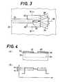
- FIG. 3shows one of a plurality of branching portions of a three-dimensional waveguide of the deflector portion provided on a substrate 31, which is formed of a Z-cut crystal of the same material as the substrate 10 of the preceding embodiment.
- a main path 34 of the waveguideis bent at each branching portion, on one side of a centerline 36, by a predetermined angle ⁇ with respect to the centerline 36.
- the centerline 36passes a branch point 32 of the branching portion and is parallel to the direction of propagation of the laser beam through the waveguide.
- a branch path 38diverges from the main path 34 at the branch point 32, on the other side of the centerline 36, such that an angle formed by the branch path 38 and the centerline 36 is equal to the angle 8.
- the branch path 38, and the corresponding bent portion of the main path 34 downstream of the branch point 32are formed symmetrically with each other with respect to the centerline 36.
- a pair of spaced-apart deflector electrodes 40, 42are formed on the substrate 31 via respective buffer layers 44, 46, such that the electrodes 40, 42 are partly disposed over the main path 34, as indicated in Fig. 4(a).
- deflector electrodes 40, 42are positioned, dimensioned and shaped so that each electrode 40, 42 extends between two points upstream and downstream of the branch point 32 over a predetermined length, generally in the direction parallel to the centerline 36, and such that the distance between the opposite inner edges of the two electrodes 40, 42 decreases as the electrodes extend in the downstream direction of the waveguide 34, 38.
- the electrode 40is grounded while the electrode 42 is subject to a positive voltage, for example, so that there is established a distribution of a refractive index, as indicated in Fig. 4(b), in the direction of width of the main path 34 of the waveguide in the branching portion, e.g., in the cross section of Fig. 4(a) including the branch point 32.
- the Z-cut crystal substrate 31has a property that its refractive index is varied sensitively as a function of the magnitude of an electric field in the Z-axis direction, i.e., in the direction of thickness of the substrate 31.
- the refractive index of the main path 34 in the width directionis accordingly different. More specifically, assuming the main path 34 has a refractive index N , the refractive indexes of the portions of the main path 34 corresponding to the electrodes 40 and 42 upon application of a voltage to the electrode 42 are N o - ⁇ N, and N + ⁇ N, respectively, as indicated in solid lines in Fig. 4(b). A dashed line in Fig. 4(b) represents the refractive index while no voltage is applied to the electrode 42.
- the rays of laser light passing through the right and left portions of the main path 34experience the different refractive indexes (N o - ⁇ N, and N 0 + AN), in the branching portion (in the vicinity of the branch point 32), whereby the laser beam passing through the main path 34 is deflected into the branch path 38, as in the preceding embodiment.
- the branching portion in questionhas the distribution of refractive index as indicated in one-dot chain line in Fig. 4(b), which distribution is reversed with respect to that established when a positive voltage is applied to the electrode 42, as described above.
- the laser beamis deflected into the bent portion of the main path 34.
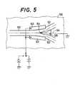
- FIG. 5A further modified embodiment of the invention is illustrated in Fig. 5, wherein a branch path 52 diverges from a main path 50 at a branch point 64, at a predetermined angle with respect to a centerline 54, such that the branch path 52 is symmetrical with a bent portion of the main path 50 with respect to the centerline 54, in the same manner as in the preceding embodiment of Fig. 3.
- the centerline 54passes the branch point 64 and is parallel to the direction of propagation of the laser beam through the waveguide.
- a substrate 56is formed of a Y-cut crystal which has a property that its refractive index is varied sensitively as a function of the magnitude of an electric field in the Y-axis direction (in the direction perpendicular to the direction of propagation of the laser beam through the waveguide).
- a central electrode 58On this substrate 56, there are formed a central electrode 58 and a pair of side electrodes 60, 62, as shown in Fig. 5.
- the central electrode 58has a generally triangular shape, and is disposed in alignment with the centerline 54, such that its apex is located at the branch point 64 on the centerline 54. That is, the width of the central electrode 58 increases in the direction of propagation of the laser beam.
- the side electrodes 60, 62are positioned on opposite sides of the centerline 54 so as to sandwich the branching portion of the waveguide (in the vinicity of the branch point 64), such that the portions of the electrodes 60, 62 downstream of the branch point 64 are spaced from the central electrode 58 in the direction of width of the waveguide.
- a positive voltageis applied across the side electrodes 60 while the central electrode 58 is held grounded.
- electric fieldsare produced between the side electrode 60, 62 and the central electrode 5, and between the side electrode 62 and the central electrode 58. Since these electric fields are formed in the- opposite Y-axis directions, the refractive index of the branching portion of the waveguide is changed in the Y-axis direction (perpendicular to the direction of propagation of the laser beam), whereby the refractive index of the branching portion has a distribution similar to that shown in Fig. 4(b).
- the laser beam passing through the main path 50is deflected at the branch point 64 and directed into the branch path 52.
- the substrate 10, 31, 56may consists of a base made of LiTao 3 having a relatively low electro-optical effect, or Sio 2 having no electro-optical effect, and a comparatively thin layer formed on the base and made of a material which has a relatively high electro-optical effect.
- the configuration of the outer and inner electrodes 26, 28 provided as deflector electrode means of the first embodiment of Figs. 1-2may be modified as necessary, provided that an area located between the outer and inner electrodes contains an outer part of the main path on the side of the corresponding branch path, at each branching portion of the waveguide.
- the two electrodesare configurated and positioned such that an area between the two electrodes also contains an outer part of the branch path on the same side of the above-indicated part of the main path.
- the laser chip 14may be replaced by a combination of a laser source, and an optical fiber which is connected at its one end to the laser source and at the other end to the incoming end of the condenser portion 16.
- the toroidal lens 30is used in the illustrated embodiments, the lens 30 may be eliminated, where the size of a spot of the laser beam to be formed on the subject surface need not be so small. Further, other suitable optical elements may be substituted for the toroidal lens 30.
Landscapes
- Physics & Mathematics (AREA)
- Nonlinear Science (AREA)
- General Physics & Mathematics (AREA)
- Optics & Photonics (AREA)
- Optical Integrated Circuits (AREA)
Abstract
Description
- The present invention relates generally to an optical deflector device for deflecting a light beam, and more particularly to a technique for deflecting a light beam due to an electro-optical effect of an electro-optical material, without using mechanical moving parts.
- An optical deflector for deflecting a light beam within a predetermined angular range is used in various devices such as a laser-beam printer and a bar code reader. Known as typical examples of such a light deflector are a polygon mirror and a hologram scanner. These deflectors use mechanical moving parts such as a rotary mechanism and a device for driving the rotary mechanism. Thus, these optical deflector devices tend to be complicated in construction, relatively large-sized, and are not satisfactory in durability.
- It is accordingly an object of the present invention to provide an optical deflector which does not incorporate mechanical moving parts, and which is simple in construction, relatively small-sized and durable.
- According to the present invention, there is provided an optical deflector for deflecting a light beam within a predetermined range of angle, including a substrate having an electro-optical effect, a three-dimensional waveguide formed on one of opposite surfaces of the substrate, to guide waves of the light beam therethrough, and a plurality of deflector electrode means. The waveguide includes a main path, and a plurality of branch paths diverging from the main path at respective branching portions of the waveguide. The branch paths are angled with respect to the main path so as to cover the predetermined range of angle. Each of the plurality of deflector electrode means is disposed at a corresponding one of the branching portions of the three-dimensional waveguide. Upon selective application of an electric voltage to each deflector electrode means, the deflector electrode means produces an electric field locally at the corresponding branching portion of the waveguide, and thereby deflect the light beam from the main path into a corresponding one of the plurality of branch paths, due to the electro-optical effect of the substrate.
- In the optical deflector of the present invntion constructed as described above, the refractive index of a part of the main path at each branching portion of the three-dimensional waveguide is increased when an electric field is locally produced at that branching portion due to an electro-optical effect of the substrate upon selective application of a voltage to the corresponding deflector electrode means. Therefore, the rays of the light beam which propagate through the above-indicated part of the main path are subject to a higher refractive index and are consequently deflected from the main path into the corresponding branch path, whereby the deflected light rays are passed through the branch path which diverges from the main path at a given angle.
- In the above arrangement of the invention, the light beam propagating through the main path of the waveguide can be deflected into a selected one of the plurality of branch paths, by applying a suitable voltage to the appropriate deflector electrode means. Thus, the light beam may be deflected within the predetermined range of angle with respect to the main path.
- According to one feature of the present invention, each deflector electrode means comprises a pair of generally elongate electrodes consisting of an inner electrode and an outer electrode. The inner electrode is disposed on the corresponding branching portion of the waveguide so as to extend parallel to the main path and the corresponding branch path. The outer electrode is spaced a predetermined distance from the inner electrode so as to be located outside the waveguide and extend substantially parallel to the inner electrode.
- In accordance with another feature of the invention, each of the branch paths diverges from the main path at a branch point of the corresponding branching portion, symmetrically with a corresponding portion of the main path, with respect to a centerline which passes the branch point and which is parallel to a direction of propagation of the light beam through the waveguide. Each deflector electrode means comprises a pair of electrodes which are disposed on opposite sides of the centerline, symmetrically with each other with respect to the centerline, so as to extend between two points upstream and downstream of the branch point, such that a distance between the pair of electrodes decreases in a downstream direction of the waveguide.
- According to a further feature of the invention, each of the branch paths diverges from the main path symmetrically with the corresponding portion of the main path, with respect to the centerline, as described above. In this case, however, each deflector electrode means comprises a central electrode having a generally triangular shape, and a pair of side electrodes. The central electrode is disposed in alignment with the centerline such that an apex of the central electrode is positioned in the vicinity of the branch point, whereby a width of the central electrode increases in a downstream direction of the waveguide. The side electrodes are disposed on opposite sides of the centerline symmetrically with each other with respect to the centerline, so as to sandwich the corresponding branching portion of the waveguide such that a portion of each side electrode on the downstream side of the branch point is spaced from the central electrode, in the direction perpendicular to said direction of propagation of the light beam..
- According to a still further feature of the invention, the three-dimensional waveguide has a refractive index which increases in a direction toward a centerline thereof, in a plane perpendicular to a direction of propagation of the light beam through the waveguide, so that the waves of the light beam are trapped in directions of thickness and width of the substrate in the plane.
- According to a yet further feature of the invention, the substrate consists of a single crystal ofLiNb03,
- According to another aspect of the present invention, there is provided an optical deflector for deflecting a light beam within a predetermined range of angle, including a substrate having an electro-optical effect, a semi-conductor laser element fixed at one of opposite ends of the substrate, a condenser portion formed on one of opposite surfaces of the substrate, and a deflector portion. The semi-conductor element is adapted to emit a laser radiation from the above-indicated one end of the substrate so that the radiation propagates along a plane of the substrate. The condenser portion is disposed adjacent to the semi-conductor laser element, to condense the laser radiation into parallel rays of laser light. The deflector portion includes a three-dimensional waveguide formed on the above-indicated one of opposite surfaces of the substrate, and a plurality of deflector electrode means. The waveguide is formed to guide therethrough the parallel rays of laser light from the condenser. The waveguide includes a main path, and a plurality of branch paths diverging from the main path at respective branching portions of the waveguide. The branch paths are angled with respect to the main path so as to cover the predetermined range of angle. Each of the plurality of deflector electrode means is disposed at a corresponding one of the branching portions of the three-dimensional waveguide. Each deflector electrode means is adapted to produce an electric field locally at the corresponding branching portion of the waveguide, and thereby deflect the light beam from the main path into a corresponding one of the plurality of branch paths, due to the electro-optical effect of the substrate upon selective application of a voltage to each deflector electrode means.
- According to one feature of the above aspect of the present invention, the condenser portion is formed by diffusion of a metal through a part of the substrate from the above-indicated one of opposite surfaces of the substrate, so as to give the condenser portion a refractive index which increases toward its center in opposite directions perpendicular to a direction of propagation of the parallel rays of laser light.
- In accordance with another feature of the same aspect of the invention, the optical deflector further comprises a toroidal lens for converging the laser light emitted selectively from the ends of the main path and the branch paths of the waveguide which are located at the other of the opposite ends of the substrate remote from the semi-conductor laser element.
- The foregoing and optional objects, features and advantages of the present invention will be better understood by reading the following description of preferred embodiments of the invention, when considered in connection with the accompanying drawings, in which:
- . Fig. 1 is a perspective view of an arrangement of an optical defletor according to one embodiment of the present invention;
- Fig. 2 is a fragmentary enlarged view showing in detail branching portions of a three-dimensional waveguide of the optical deflector of Fig. 1;
- Fig. 3 is a view corresponding to Fig. 2, showing another embodiment of an optical deflector of the invention;
- Fig. 4(a) is an enlarged view in cross section taken along line 4-4 of Fig. 3;
- Fig. 4(b) is a view showing a distribution of a refractive index of a branching portion of the optical deflector, as seen in the cross section of Fig. 4(a); and
- Fig. 5 is a view also corresponding to Fig. 2, showing a further modified embodiment of the invention.
- The preferred embodiments of the invention will now be described in detail, by reference to the accompanying drawings.
- Referring to Fig. 1, there is shown a
rectangular substrate 10 in the form of a translucent plate which is made of an electro-optical material having an electro-optical effect. For example, thesubstrate 10 is formed of a single crystal of LiNb03. On one of the opposite major surfaces of therectangular substrate 10, there are formed acondenser portion 16 disposed adjacent to one of the opposite longutidinal ends of thesubstrate 10, and adeflector portion 18 disposed between thecondenser portion 16 and the other longitudinal end of thesubstrate 10. - On the end face of the
substrate 10 at the above-indicated one longitudinal end, there is fixed a semi-conductor laser element in the form of achip 14 which emits a laser radiation so that the radiation is incident upon thecondenser portion 16. Thecondenser portion 16 is adapted to function as a convex lens for condensing condense the incident radiation from thelaser chip 14 into parallel rays of laser light. Thiscondenser portion 16 is formed by diffusion of a suitable metal such as Ti through a part of thesubstrate 10 from the upper major surface, such that thecondenser portion 16 has a refractive index which increases toward its center in opposite directions along the width of thesubstrate 10, i.e., in opposite directions perpendicular to the direction of propagation of the parallel rays of laser light emitted from thecondenser portion 16. While thecondenser portion 16 cannot be visually distinguished from thesubstrate 10, its continuously varying refractive index is indicated by parallel straight lines in Fig. 1. The density of the straight lines indicates the refractive index. Thecondenser portion 16 may be replaced by a geodesic lens provided in the form of a part-spherical concave cavity formed in the upper major surface of thesubstrate 10. - The
deflector portion 18 has a three-dimensional waveguide generally indicated at 24. Thewaveguide 24 consists of a straightmain path 20 which receives the parallel rays of laser light from thecondenser portion 16, and a plurality ofstraight branch paths 22 which diverge from themain path 20 alternately on opposite sides of themain path 20. More specifically, thebranch paths 22 branch from respective branching portions 23 (23a, 23b, etc.) of thewaveguide 24, which are spaced apart from each other along themain path 18, as indicated in Fig. 2. The ends of thebranch paths portions substrate 10 remote from thelaser chip 14. The angles of thebranch paths 22 with respect to themain path 20, and the locations of the branching portions 23 in the direction of the length of themain path 20 are determined so that the ends of thebranch paths 22 cover a predetermined angular range of deflection of the laser beam. The angle of eachbranch path 22 to themain path 20 corresponds to an angle of deflection of the laser beam at the corresponding branching portion 23. The main andbranch paths dimensional waveguide 24 have a refractive index which increases in a direction toward its centerline, in a plane perpendicular to the direction of propagation of the laser beam through thepaths substrate 10. While the three-dimensional waveguide 24 having a higher refractive index cannot be visually distinguished from thesubstrate 10, the main andbranch paths - A pair of generally elongate parallel deflector electrodes 26, 28 are disposed at each branching portion 23, for deflecting the parallel rays of laser into the
corresponding branch path 22. Each pair of deflector electrodes 26, 28 consist of an outer electrode 26, and an inner electrode 28 having a smaller width than that of the main andbranch paths outer electrode 26a at the branchingportion 23a, for example, is disposed outside thewaveguide 24, so as to extend along the outer edges of themain path 20 and thecorresponding branch path 22a, with a suitable distance from the outer edges. The correspondinginner electrode 28a at the branchingportion 23a is disposed on the centerlines of themain path 20 and thebranch path 22a, so as to extend parallel to theouter electrode 26a. That is, the outer andinner electrodes branch paths inner electrodes branch paths inner electrodes portion 23b adjacent to the branchingportion 23a, are disposed in the same manner. - The optical deflector constructed as described above may be used for a laser-beam printer or an optical image reader, for example. A
toroidal lens 30 is disposed between the end of thesubstrate 10 remote from thelaser chip 14, and a photosensitive drum surface of the laser-beam printer or a medium surface to be read by the image reader, so that the drum surface or medium surface is scanned by the laser beam which is swept by the instant optical deflector. The laser beam emitted from the end of eachbranch path 22 of thewaveguide 24 is converged by thetoroidal lens 30, and thus focused or concentrated at a point on the photosensitive drum surface or medium surface. - There will be described the operation of the present optical deflector for deflecting or sweeping a laser beam over a predetermined angular range.
- As previously described, the parallel rays of laser light from the
condenser portion 16 are introduced into themain path 20 of the three-dimensional waveguide 24. If none of the electrode pairs 26, 28 at the branching portions 23 are energized, the rays are passed through the straightmain path 20, without deflection into anybranch paths 22. As a result, the laser rays are emitted from the end of themain path 20 at the end of thesubstrate 10 remote from thesemi-conductor laser chip 14. If an electric voltage of a suitable level is applied between the outer andinner electrodes portion 23a, for example, the outer part of themain path 20 located between the outer andinner electrodes main path 20, due to an electro-optical effect. - Generally, an electro-optical material has a refractive index which is varied with a magnitude of an electric field in which the material is placed. In the case where the
substrate 10 is formed of a Z-cut crystal, a variation Δn in refractive index of a portion of thesubstrate 10 between the energized outer and inner electrodes 26, 28 is expressed by the following equation (1):
- where, n : refractive index of the
substrate 10 with respect to abnormal light - n33: electro-optical constant of the
substrate 10 in the direction of thickness - The above equation (1) indicates that the refractive index of the portion of the
substrate 10 between the two electrodes 26 and 28, i.e., refractive index of the part of themain path 20 of thewaveguide 24 between the twoelectrodes main path 20, when an electric voltage is applied between the twoelectrodes - Therefore, the laser rays which propagate in the above-indicated part of the
main path 20 experience a comparatively higher refractive index, whereby the laser beam as a whole is deflected on the side of theouter electrode 26a, and thereby directed into the correspondingbranch path 22a. The laser beam thus introduced into thebranch path 22a is guided through thisbranch path 22a, and emitted from its end toward thetoroidal lens 30. In this manner, the laser beam is deflected by an angle corresponding to the angle of thebranch path 22a with respect to themain path 20. - Thus, the laser beam may be deflected at a desired angle, by selecting one of the branching portions 23, namely, by applying an electric voltage between the outer and inner electrodes 26 and 28 at the selected branching portion 23. In this connection, it is noted that the spacings between the adjacent branching portions 23 along the
main path 20, and the angles of thebranch paths 22 relative to themain path 20 are determined so that the laser beam emitted from thebranch paths 22 may cover a desired sweep range of the optical deflector, as previously indicated. - As discussed above, the
deflector portion 18 of the illustrated optical deflector is adapted to deflect a laser beam by changing the refractive index of themain path 20 of the three-dimensional waveguide 24, locally at the selected branching portion 23, through the utilization of an electro-optical effect of the material which constitutes thewaveguide 24. This local change in the refractive index is achieved by applying an electric voltage to one of the plurality of electrode pairs 26, 28 at the selected branching portion 23. Hence, the instant optical deflector has eliminated any mechanical moving parts as used in a rotary mechanism and a rotary driving device employed in the conventional optical deflector. The elimination of such mechanical parts assures improved operating reliability and durability of the optical deflector, and noise-free operation of the deflector. These are some of the advantages offered by the present optical deflector. - Another embodiment of the invention will be described referring to Fig. 3 and Figs. 4(a) and 4(b). More specifically, Fig. 3 shows one of a plurality of branching portions of a three-dimensional waveguide of the deflector portion provided on a
substrate 31, which is formed of a Z-cut crystal of the same material as thesubstrate 10 of the preceding embodiment. In the present modified embodiment, amain path 34 of the waveguide is bent at each branching portion, on one side of acenterline 36, by a predetermined angle θ with respect to thecenterline 36. The centerline 36 passes abranch point 32 of the branching portion and is parallel to the direction of propagation of the laser beam through the waveguide. A branch path 38 diverges from themain path 34 at thebranch point 32, on the other side of thecenterline 36, such that an angle formed by the branch path 38 and thecenterline 36 is equal to the angle 8. Namely, the branch path 38, and the corresponding bent portion of themain path 34 downstream of thebranch point 32 are formed symmetrically with each other with respect to thecenterline 36. In each branching portion of the waveguide as described above, a pair of spaced-apartdeflector electrodes substrate 31 via respective buffer layers 44, 46, such that theelectrodes main path 34, as indicated in Fig. 4(a). Thesedeflector electrodes electrode branch point 32 over a predetermined length, generally in the direction parallel to thecenterline 36, and such that the distance between the opposite inner edges of the twoelectrodes waveguide 34, 38. - In the present embodiment, the
electrode 40 is grounded while theelectrode 42 is subject to a positive voltage, for example, so that there is established a distribution of a refractive index, as indicated in Fig. 4(b), in the direction of width of themain path 34 of the waveguide in the branching portion, e.g., in the cross section of Fig. 4(a) including thebranch point 32. Described more particularly, the Z-cut crystal substrate 31 has a property that its refractive index is varied sensitively as a function of the magnitude of an electric field in the Z-axis direction, i.e., in the direction of thickness of thesubstrate 31. Since the magnitude of the electric field in the direction of thickness upon application of a voltage to theelectrode 42 is different locally in the direction of width of themain path 34, the refractive index of themain path 34 in the width direction is accordingly different. More specifically, assuming themain path 34 has a refractive index N , the refractive indexes of the portions of themain path 34 corresponding to theelectrodes electrode 42 are No - ΔN, and N + ΔN, respectively, as indicated in solid lines in Fig. 4(b). A dashed line in Fig. 4(b) represents the refractive index while no voltage is applied to theelectrode 42. In the arrangement described above, the rays of laser light passing through the right and left portions of the main path 34 (as viewed in the direction of propagation of the laser light) experience the different refractive indexes (No - ΔN, and N0 + AN), in the branching portion (in the vicinity of the branch point 32), whereby the laser beam passing through themain path 34 is deflected into the branch path 38, as in the preceding embodiment. - On the other hand, when the
electrode 42 is grounded while theelectrode 40 is subject to a positive voltage, the branching portion in question has the distribution of refractive index as indicated in one-dot chain line in Fig. 4(b), which distribution is reversed with respect to that established when a positive voltage is applied to theelectrode 42, as described above. As a result, the laser beam is deflected into the bent portion of themain path 34. - A further modified embodiment of the invention is illustrated in Fig. 5, wherein a
branch path 52 diverges from amain path 50 at abranch point 64, at a predetermined angle with respect to acenterline 54, such that thebranch path 52 is symmetrical with a bent portion of themain path 50 with respect to thecenterline 54, in the same manner as in the preceding embodiment of Fig. 3. The centerline 54 passes thebranch point 64 and is parallel to the direction of propagation of the laser beam through the waveguide. In the present embodiment, asubstrate 56 is formed of a Y-cut crystal which has a property that its refractive index is varied sensitively as a function of the magnitude of an electric field in the Y-axis direction (in the direction perpendicular to the direction of propagation of the laser beam through the waveguide). On thissubstrate 56, there are formed acentral electrode 58 and a pair ofside electrodes central electrode 58 has a generally triangular shape, and is disposed in alignment with thecenterline 54, such that its apex is located at thebranch point 64 on thecenterline 54. That is, the width of thecentral electrode 58 increases in the direction of propagation of the laser beam. Theside electrodes centerline 54 so as to sandwich the branching portion of the waveguide (in the vinicity of the branch point 64), such that the portions of theelectrodes branch point 64 are spaced from thecentral electrode 58 in the direction of width of the waveguide. - In the present modified embodiment, a positive voltage is applied across the
side electrodes 60 while thecentral electrode 58 is held grounded. As a result, electric fields are produced between theside electrode side electrode 62 and thecentral electrode 58. Since these electric fields are formed in the- opposite Y-axis directions, the refractive index of the branching portion of the waveguide is changed in the Y-axis direction (perpendicular to the direction of propagation of the laser beam), whereby the refractive index of the branching portion has a distribution similar to that shown in Fig. 4(b). Thus, the laser beam passing through themain path 50 is deflected at thebranch point 64 and directed into thebranch path 52. - On the other hand, when a negative voltage is applied across the
side electrodes main path 34. - While the present invention has been described in its preferred embodiments by refereence to the figures of the drawings, it is to be understood that the invention may be otherwise embodied.
- For example, the
substrate - Further, the configuration of the outer and inner electrodes 26, 28 provided as deflector electrode means of the first embodiment of Figs. 1-2 may be modified as necessary, provided that an area located between the outer and inner electrodes contains an outer part of the main path on the side of the corresponding branch path, at each branching portion of the waveguide. Preferably, the two electrodes are configurated and positioned such that an area between the two electrodes also contains an outer part of the branch path on the same side of the above-indicated part of the main path.
- While the illustrated embodiments use a semi-conductor laser element in the form of the
laser chip 14 attached at one end face of the substrate, thelaser chip 14 may be replaced by a combination of a laser source, and an optical fiber which is connected at its one end to the laser source and at the other end to the incoming end of thecondenser portion 16. - Although the
toroidal lens 30 is used in the illustrated embodiments, thelens 30 may be eliminated, where the size of a spot of the laser beam to be formed on the subject surface need not be so small. Further, other suitable optical elements may be substituted for thetoroidal lens 30. - It is further understood that the form of the invention herein described and shown is to be taken as a preferred example of the same, and that various changes and modifications may be restorted to without departing from the spirit and scope of the invention.

Claims (9)
Applications Claiming Priority (2)
| Application Number | Priority Date | Filing Date | Title |
|---|---|---|---|
| JP171986/85 | 1985-08-05 | ||
| JP60171986AJPS6232425A (en) | 1985-08-05 | 1985-08-05 | optical deflector |
Publications (2)
| Publication Number | Publication Date |
|---|---|
| EP0212904A1true EP0212904A1 (en) | 1987-03-04 |
| EP0212904B1 EP0212904B1 (en) | 1991-02-13 |
Family
ID=15933414
Family Applications (1)
| Application Number | Title | Priority Date | Filing Date |
|---|---|---|---|
| EP86305998AExpired - LifetimeEP0212904B1 (en) | 1985-08-05 | 1986-08-04 | Optical deflector |
Country Status (4)
| Country | Link |
|---|---|
| US (1) | US4765703A (en) |
| EP (1) | EP0212904B1 (en) |
| JP (1) | JPS6232425A (en) |
| DE (1) | DE3677521D1 (en) |
Families Citing this family (60)
| Publication number | Priority date | Publication date | Assignee | Title |
|---|---|---|---|---|
| US5018813A (en)* | 1990-05-01 | 1991-05-28 | Eastman Kodak Company | Multichannel integrated optic modulator for laser printer |
| US5317446A (en)* | 1992-09-29 | 1994-05-31 | Eastman Kodak Company | Electrooptic device for scanning using domain reversed regions |
| US5305412A (en)* | 1992-12-14 | 1994-04-19 | Xerox Corporation | Semiconductor diode optical switching arrays utilizing low-loss, passive waveguides |
| US5371817A (en)* | 1993-02-16 | 1994-12-06 | Eastman Kodak Company | Multichannel optical waveguide page scanner with individually addressable electro-optic modulators |
| US6341118B1 (en)* | 1998-06-02 | 2002-01-22 | Science Applications International Corporation | Multiple channel scanning device using oversampling and image processing to increase throughput |
| US6584052B1 (en) | 1998-06-02 | 2003-06-24 | Science Applications International Corporation | Method and apparatus for controlling the focus of a read/write head for an optical scanner |
| US6480323B1 (en) | 1998-12-18 | 2002-11-12 | Carnegie Mellon University | Two-dimensional beam scanner |
| US7149383B2 (en) | 2003-06-30 | 2006-12-12 | Finisar Corporation | Optical system with reduced back reflection |
| US6961489B2 (en)* | 2003-06-30 | 2005-11-01 | Finisar Corporation | High speed optical system |
| GB0522968D0 (en) | 2005-11-11 | 2005-12-21 | Popovich Milan M | Holographic illumination device |
| GB0718706D0 (en) | 2007-09-25 | 2007-11-07 | Creative Physics Ltd | Method and apparatus for reducing laser speckle |
| US11726332B2 (en) | 2009-04-27 | 2023-08-15 | Digilens Inc. | Diffractive projection apparatus |
| US9335604B2 (en) | 2013-12-11 | 2016-05-10 | Milan Momcilo Popovich | Holographic waveguide display |
| US11204540B2 (en) | 2009-10-09 | 2021-12-21 | Digilens Inc. | Diffractive waveguide providing a retinal image |
| US20200057353A1 (en) | 2009-10-09 | 2020-02-20 | Digilens Inc. | Compact Edge Illuminated Diffractive Display |
| WO2012136970A1 (en) | 2011-04-07 | 2012-10-11 | Milan Momcilo Popovich | Laser despeckler based on angular diversity |
| US10670876B2 (en) | 2011-08-24 | 2020-06-02 | Digilens Inc. | Waveguide laser illuminator incorporating a despeckler |
| WO2016020630A2 (en) | 2014-08-08 | 2016-02-11 | Milan Momcilo Popovich | Waveguide laser illuminator incorporating a despeckler |
| EP2995986B1 (en) | 2011-08-24 | 2017-04-12 | Rockwell Collins, Inc. | Data display |
| US20150010265A1 (en) | 2012-01-06 | 2015-01-08 | Milan, Momcilo POPOVICH | Contact image sensor using switchable bragg gratings |
| CN106125308B (en) | 2012-04-25 | 2019-10-25 | 罗克韦尔柯林斯公司 | Device and method for displaying images |
| WO2013167864A1 (en) | 2012-05-11 | 2013-11-14 | Milan Momcilo Popovich | Apparatus for eye tracking |
| US9933684B2 (en) | 2012-11-16 | 2018-04-03 | Rockwell Collins, Inc. | Transparent waveguide display providing upper and lower fields of view having a specific light output aperture configuration |
| US10209517B2 (en) | 2013-05-20 | 2019-02-19 | Digilens, Inc. | Holographic waveguide eye tracker |
| WO2015015138A1 (en) | 2013-07-31 | 2015-02-05 | Milan Momcilo Popovich | Method and apparatus for contact image sensing |
| KR101675193B1 (en)* | 2014-04-25 | 2016-11-11 | 한국과학기술원 | Three dimensional optical interconnecting structure using branched waveguides |
| US10359736B2 (en) | 2014-08-08 | 2019-07-23 | Digilens Inc. | Method for holographic mastering and replication |
| WO2016042283A1 (en) | 2014-09-19 | 2016-03-24 | Milan Momcilo Popovich | Method and apparatus for generating input images for holographic waveguide displays |
| EP3198192A1 (en) | 2014-09-26 | 2017-08-02 | Milan Momcilo Popovich | Holographic waveguide opticaltracker |
| US20180275402A1 (en) | 2015-01-12 | 2018-09-27 | Digilens, Inc. | Holographic waveguide light field displays |
| WO2016113534A1 (en) | 2015-01-12 | 2016-07-21 | Milan Momcilo Popovich | Environmentally isolated waveguide display |
| EP3248026B1 (en) | 2015-01-20 | 2019-09-04 | DigiLens Inc. | Holographic waveguide lidar |
| US9632226B2 (en) | 2015-02-12 | 2017-04-25 | Digilens Inc. | Waveguide grating device |
| WO2016146963A1 (en) | 2015-03-16 | 2016-09-22 | Popovich, Milan, Momcilo | Waveguide device incorporating a light pipe |
| WO2016156776A1 (en) | 2015-03-31 | 2016-10-06 | Milan Momcilo Popovich | Method and apparatus for contact image sensing |
| CN113759555B (en) | 2015-10-05 | 2024-09-20 | 迪吉伦斯公司 | Waveguide Display |
| CN109073889B (en) | 2016-02-04 | 2021-04-27 | 迪吉伦斯公司 | Holographic waveguide optical tracker |
| CN108780224B (en) | 2016-03-24 | 2021-08-03 | 迪吉伦斯公司 | Method and apparatus for providing a polarization selective holographic waveguide device |
| US10890707B2 (en) | 2016-04-11 | 2021-01-12 | Digilens Inc. | Holographic waveguide apparatus for structured light projection |
| WO2018102834A2 (en) | 2016-12-02 | 2018-06-07 | Digilens, Inc. | Waveguide device with uniform output illumination |
| US10545346B2 (en) | 2017-01-05 | 2020-01-28 | Digilens Inc. | Wearable heads up displays |
| WO2019079350A2 (en) | 2017-10-16 | 2019-04-25 | Digilens, Inc. | Systems and methods for multiplying the image resolution of a pixelated display |
| WO2019136476A1 (en) | 2018-01-08 | 2019-07-11 | Digilens, Inc. | Waveguide architectures and related methods of manufacturing |
| US10732569B2 (en) | 2018-01-08 | 2020-08-04 | Digilens Inc. | Systems and methods for high-throughput recording of holographic gratings in waveguide cells |
| EP3710894B1 (en) | 2018-01-08 | 2025-07-30 | Digilens Inc. | Methods for fabricating optical waveguides |
| EP3710876A4 (en) | 2018-01-08 | 2022-02-09 | DigiLens Inc. | SYSTEMS AND METHODS OF FABRICATING WAVEGUIDE CELLS |
| US10690851B2 (en) | 2018-03-16 | 2020-06-23 | Digilens Inc. | Holographic waveguides incorporating birefringence control and methods for their fabrication |
| WO2020023779A1 (en) | 2018-07-25 | 2020-01-30 | Digilens Inc. | Systems and methods for fabricating a multilayer optical structure |
| US20200225471A1 (en) | 2019-01-14 | 2020-07-16 | Digilens Inc. | Holographic Waveguide Display with Light Control Layer |
| US20200247017A1 (en) | 2019-02-05 | 2020-08-06 | Digilens Inc. | Methods for Compensating for Optical Surface Nonuniformity |
| KR102866596B1 (en) | 2019-02-15 | 2025-09-29 | 디지렌즈 인코포레이티드. | Method and device for providing a holographic waveguide display using an integral grating |
| US20220283377A1 (en) | 2019-02-15 | 2022-09-08 | Digilens Inc. | Wide Angle Waveguide Display |
| WO2020186113A1 (en) | 2019-03-12 | 2020-09-17 | Digilens Inc. | Holographic waveguide backlight and related methods of manufacturing |
| EP3980825A4 (en) | 2019-06-07 | 2023-05-03 | Digilens Inc. | WAVEGUIDES WITH TRANSMITTING AND REFLECTING GRIDS AND RELATED MANUFACTURING PROCESSES |
| EP4004646A4 (en) | 2019-07-29 | 2023-09-06 | Digilens Inc. | METHODS AND APPARATUS FOR MULTIPLYING THE IMAGE RESOLUTION AND FIELD OF VIEW OF A PIXELATED DISPLAY SCREEN |
| KR102775783B1 (en) | 2019-08-29 | 2025-02-28 | 디지렌즈 인코포레이티드. | Vacuum grid and method for manufacturing the same |
| US11550033B2 (en)* | 2020-05-28 | 2023-01-10 | Beijing Voyager Technology Co., Ltd. | Electro-optical beam deflecting unit for light detection and ranging (LiDAR) |
| JP2024502255A (en) | 2020-12-21 | 2024-01-18 | ディジレンズ インコーポレイテッド | Eye glow suppression in waveguide-based displays |
| WO2022150841A1 (en) | 2021-01-07 | 2022-07-14 | Digilens Inc. | Grating structures for color waveguides |
| US12158612B2 (en) | 2021-03-05 | 2024-12-03 | Digilens Inc. | Evacuated periodic structures and methods of manufacturing |
Citations (5)
| Publication number | Priority date | Publication date | Assignee | Title |
|---|---|---|---|---|
| DE2359797B2 (en)* | 1973-11-30 | 1977-12-15 | RCA Corp, New York, N.Y. (V.StA.) | SWITCHABLE OPTICAL WAVE GUIDE DEVICE |
| US4070092A (en)* | 1976-09-22 | 1978-01-24 | The United States Of America As Represented By The Secretary Of The Navy | Active waveguide branch with variable synchronism |
| US4175827A (en)* | 1978-02-21 | 1979-11-27 | Sperry Rand Corporation | Electro-optical multiplexer having multiple frequency resonant excitation |
| US4478843A (en)* | 1980-11-06 | 1984-10-23 | Hoechst Aktiengesellschaft | 5-Phenyltetrazoles and their use as salidiuretics |
| DE3443863A1 (en)* | 1983-12-02 | 1985-06-13 | Canon K.K., Tokio/Tokyo | ELEMENT WITH LIGHTWAVE GUIDES AND METHOD FOR THE PRODUCTION THEREOF |
Family Cites Families (18)
| Publication number | Priority date | Publication date | Assignee | Title |
|---|---|---|---|---|
| US3795433A (en)* | 1972-05-22 | 1974-03-05 | Rca Corp | Voltage induced optical waveguide means |
| CH558572A (en)* | 1972-08-10 | 1975-01-31 | Zellweger Uster Ag | OPTICAL SCANNING DEVICE. |
| JPS518949A (en)* | 1974-07-10 | 1976-01-24 | Canon Kk | REEZAKIROKU SOCHI |
| JPS54150153A (en)* | 1978-05-17 | 1979-11-26 | Ricoh Co Ltd | Multifrequency driving acousto-optic element |
| NL7904724A (en)* | 1979-06-18 | 1980-12-22 | Philips Nv | OPTICAL SCANNER WITH FOCUSING SYSTEM. |
| FR2459986A1 (en)* | 1979-06-22 | 1981-01-16 | Commissariat Energie Atomique | INTEGRATED FRESNEL LENS |
| US4425023A (en)* | 1980-01-31 | 1984-01-10 | Canon Kabushiki Kaisha | Beam spot scanning device |
| US4348079A (en)* | 1980-04-08 | 1982-09-07 | Xerox Corporation | Acousto-optic device utilizing Fresnel zone plate electrode array |
| DE3116426A1 (en)* | 1980-04-26 | 1982-02-25 | Canon K.K., Tokyo | "BEAM DEFLECTOR" |
| US4484319A (en)* | 1980-09-19 | 1984-11-20 | Matsushita Electric Industrial Co., Ltd. | Apparatus for locating a track on disc-like optical information carriers |
| US4413270A (en)* | 1981-03-30 | 1983-11-01 | Xerox Corporation | Multigate light valve for electro-optic line printers having non-telecentric imaging systems |
| JPS57198410A (en)* | 1981-06-01 | 1982-12-06 | Nippon Sheet Glass Co Ltd | Optical plane circuit equipped with optical coupler |
| JPS585718A (en)* | 1981-07-02 | 1983-01-13 | Leo Giken:Kk | Information recorder by integrated optical waveguides |
| DE3138727A1 (en)* | 1981-09-29 | 1983-04-21 | Siemens AG, 1000 Berlin und 8000 München | FREQUENCY ANALYZER IN PLANAR WAVE GUIDE TECHNOLOGY AND METHOD FOR PRODUCING A PLANAR GEODETIC LENS ON OR IN A SUBSTRATE |
| JPS58125025A (en)* | 1982-01-21 | 1983-07-25 | Omron Tateisi Electronics Co | Two-dimensional optical deflector |
| JPS58147718A (en)* | 1982-02-25 | 1983-09-02 | Omron Tateisi Electronics Co | Optical digital-to-analog converting device |
| US4478483A (en)* | 1982-05-10 | 1984-10-23 | Xerox Corporation | Variable length electro-optic waveguides and applications therefor |
| JPS59204027A (en)* | 1983-05-06 | 1984-11-19 | Canon Inc | light modulator |
- 1985
- 1985-08-05JPJP60171986Apatent/JPS6232425A/enactivePending
- 1986
- 1986-08-04EPEP86305998Apatent/EP0212904B1/ennot_activeExpired - Lifetime
- 1986-08-04USUS06/892,250patent/US4765703A/ennot_activeExpired - Lifetime
- 1986-08-04DEDE8686305998Tpatent/DE3677521D1/ennot_activeExpired - Lifetime
Patent Citations (5)
| Publication number | Priority date | Publication date | Assignee | Title |
|---|---|---|---|---|
| DE2359797B2 (en)* | 1973-11-30 | 1977-12-15 | RCA Corp, New York, N.Y. (V.StA.) | SWITCHABLE OPTICAL WAVE GUIDE DEVICE |
| US4070092A (en)* | 1976-09-22 | 1978-01-24 | The United States Of America As Represented By The Secretary Of The Navy | Active waveguide branch with variable synchronism |
| US4175827A (en)* | 1978-02-21 | 1979-11-27 | Sperry Rand Corporation | Electro-optical multiplexer having multiple frequency resonant excitation |
| US4478843A (en)* | 1980-11-06 | 1984-10-23 | Hoechst Aktiengesellschaft | 5-Phenyltetrazoles and their use as salidiuretics |
| DE3443863A1 (en)* | 1983-12-02 | 1985-06-13 | Canon K.K., Tokio/Tokyo | ELEMENT WITH LIGHTWAVE GUIDES AND METHOD FOR THE PRODUCTION THEREOF |
Also Published As
| Publication number | Publication date |
|---|---|
| US4765703A (en) | 1988-08-23 |
| EP0212904B1 (en) | 1991-02-13 |
| DE3677521D1 (en) | 1991-03-21 |
| JPS6232425A (en) | 1987-02-12 |
Similar Documents
| Publication | Publication Date | Title |
|---|---|---|
| US4765703A (en) | Optical deflector | |
| US5153770A (en) | Total internal reflection electro-optic modulator | |
| JP2689178B2 (en) | Optical waveguide device | |
| US4767170A (en) | Optical deflector device | |
| EP0387354B1 (en) | Light deflecting element | |
| US4139259A (en) | Light distributor for optical communication systems | |
| US4755036A (en) | Apparatus for deflecting light beam | |
| US4816912A (en) | Laser-beam printer with improved optical deflector | |
| US5291566A (en) | Total internal reflection electro-optic modulator for multiple axis and asymmetric beam profile modulation | |
| JPH0996842A (en) | Waveguide input/output device | |
| JPH04501323A (en) | scanning device | |
| EP0192433B1 (en) | Optical head for optical data storage and readout | |
| JPH01107213A (en) | Optical waveguide element | |
| US4792201A (en) | Optical deflector device | |
| US5048936A (en) | Light beam deflector | |
| US4929043A (en) | Light beam deflector | |
| JPH01107214A (en) | Optical waveguide element | |
| JPS61182025A (en) | Polarizer | |
| JP2666836B2 (en) | Solid state light deflector | |
| JPH04242728A (en) | Actuating method for light deflecting element | |
| JPH01178935A (en) | Optical deflector | |
| JPH0778586B2 (en) | Light deflection device | |
| JPS626575A (en) | Optical reader | |
| JP2834844B2 (en) | Optical switch array | |
| JPH01178934A (en) | Waveguide type optical deflector |
Legal Events
| Date | Code | Title | Description |
|---|---|---|---|
| PUAI | Public reference made under article 153(3) epc to a published international application that has entered the european phase | Free format text:ORIGINAL CODE: 0009012 | |
| AK | Designated contracting states | Kind code of ref document:A1 Designated state(s):DE GB NL | |
| 17P | Request for examination filed | Effective date:19870316 | |
| 17Q | First examination report despatched | Effective date:19881212 | |
| GRAA | (expected) grant | Free format text:ORIGINAL CODE: 0009210 | |
| AK | Designated contracting states | Kind code of ref document:B1 Designated state(s):DE GB NL | |
| REF | Corresponds to: | Ref document number:3677521 Country of ref document:DE Date of ref document:19910321 | |
| PLBE | No opposition filed within time limit | Free format text:ORIGINAL CODE: 0009261 | |
| STAA | Information on the status of an ep patent application or granted ep patent | Free format text:STATUS: NO OPPOSITION FILED WITHIN TIME LIMIT | |
| 26N | No opposition filed | ||
| REG | Reference to a national code | Ref country code:GB Ref legal event code:IF02 | |
| PGFP | Annual fee paid to national office [announced via postgrant information from national office to epo] | Ref country code:NL Payment date:20040803 Year of fee payment:19 | |
| PGFP | Annual fee paid to national office [announced via postgrant information from national office to epo] | Ref country code:GB Payment date:20040804 Year of fee payment:19 | |
| PGFP | Annual fee paid to national office [announced via postgrant information from national office to epo] | Ref country code:DE Payment date:20040812 Year of fee payment:19 | |
| PG25 | Lapsed in a contracting state [announced via postgrant information from national office to epo] | Ref country code:GB Free format text:LAPSE BECAUSE OF NON-PAYMENT OF DUE FEES Effective date:20050804 | |
| PG25 | Lapsed in a contracting state [announced via postgrant information from national office to epo] | Ref country code:NL Free format text:LAPSE BECAUSE OF NON-PAYMENT OF DUE FEES Effective date:20060301 Ref country code:DE Free format text:LAPSE BECAUSE OF NON-PAYMENT OF DUE FEES Effective date:20060301 | |
| GBPC | Gb: european patent ceased through non-payment of renewal fee | Effective date:20050804 | |
| NLV4 | Nl: lapsed or anulled due to non-payment of the annual fee | Effective date:20060301 |