EP0205164B1 - Semiconductor device structure - Google Patents
Semiconductor device structureDownload PDFInfo
- Publication number
- EP0205164B1 EP0205164B1EP86107956AEP86107956AEP0205164B1EP 0205164 B1EP0205164 B1EP 0205164B1EP 86107956 AEP86107956 AEP 86107956AEP 86107956 AEP86107956 AEP 86107956AEP 0205164 B1EP0205164 B1EP 0205164B1
- Authority
- EP
- European Patent Office
- Prior art keywords
- epitaxial region
- inp
- layer
- semiconductor
- gallium arsenide
- Prior art date
- Legal status (The legal status is an assumption and is not a legal conclusion. Google has not performed a legal analysis and makes no representation as to the accuracy of the status listed.)
- Expired
Links
Images

Classifications
- H—ELECTRICITY
- H10—SEMICONDUCTOR DEVICES; ELECTRIC SOLID-STATE DEVICES NOT OTHERWISE PROVIDED FOR
- H10D—INORGANIC ELECTRIC SEMICONDUCTOR DEVICES
- H10D62/00—Semiconductor bodies, or regions thereof, of devices having potential barriers
- H10D62/80—Semiconductor bodies, or regions thereof, of devices having potential barriers characterised by the materials
- H10D62/85—Semiconductor bodies, or regions thereof, of devices having potential barriers characterised by the materials being Group III-V materials, e.g. GaAs
- H10D62/852—Semiconductor bodies, or regions thereof, of devices having potential barriers characterised by the materials being Group III-V materials, e.g. GaAs being Group III-V materials comprising three or more elements, e.g. AlGaN or InAsSbP
- H—ELECTRICITY
- H10—SEMICONDUCTOR DEVICES; ELECTRIC SOLID-STATE DEVICES NOT OTHERWISE PROVIDED FOR
- H10D—INORGANIC ELECTRIC SEMICONDUCTOR DEVICES
- H10D30/00—Field-effect transistors [FET]
- H10D30/60—Insulated-gate field-effect transistors [IGFET]
- H10D30/67—Thin-film transistors [TFT]
- H10D30/6729—Thin-film transistors [TFT] characterised by the electrodes
- H10D30/6737—Thin-film transistors [TFT] characterised by the electrodes characterised by the electrode materials
- H10D30/6738—Schottky barrier electrodes
- H—ELECTRICITY
- H10—SEMICONDUCTOR DEVICES; ELECTRIC SOLID-STATE DEVICES NOT OTHERWISE PROVIDED FOR
- H10D—INORGANIC ELECTRIC SEMICONDUCTOR DEVICES
- H10D30/00—Field-effect transistors [FET]
- H10D30/60—Insulated-gate field-effect transistors [IGFET]
- H10D30/67—Thin-film transistors [TFT]
- H10D30/674—Thin-film transistors [TFT] characterised by the active materials
- H10D30/675—Group III-V materials, Group II-VI materials, Group IV-VI materials, selenium or tellurium
- H—ELECTRICITY
- H10—SEMICONDUCTOR DEVICES; ELECTRIC SOLID-STATE DEVICES NOT OTHERWISE PROVIDED FOR
- H10D—INORGANIC ELECTRIC SEMICONDUCTOR DEVICES
- H10D30/00—Field-effect transistors [FET]
- H10D30/80—FETs having rectifying junction gate electrodes
- H10D30/801—FETs having heterojunction gate electrodes
- H—ELECTRICITY
- H10—SEMICONDUCTOR DEVICES; ELECTRIC SOLID-STATE DEVICES NOT OTHERWISE PROVIDED FOR
- H10D—INORGANIC ELECTRIC SEMICONDUCTOR DEVICES
- H10D62/00—Semiconductor bodies, or regions thereof, of devices having potential barriers
- H10D62/80—Semiconductor bodies, or regions thereof, of devices having potential barriers characterised by the materials
- H10D62/85—Semiconductor bodies, or regions thereof, of devices having potential barriers characterised by the materials being Group III-V materials, e.g. GaAs
- H—ELECTRICITY
- H10—SEMICONDUCTOR DEVICES; ELECTRIC SOLID-STATE DEVICES NOT OTHERWISE PROVIDED FOR
- H10D—INORGANIC ELECTRIC SEMICONDUCTOR DEVICES
- H10D64/00—Electrodes of devices having potential barriers
- H10D64/60—Electrodes characterised by their materials
- H10D64/602—Heterojunction gate electrodes for FETs
- H—ELECTRICITY
- H10—SEMICONDUCTOR DEVICES; ELECTRIC SOLID-STATE DEVICES NOT OTHERWISE PROVIDED FOR
- H10D—INORGANIC ELECTRIC SEMICONDUCTOR DEVICES
- H10D64/00—Electrodes of devices having potential barriers
- H10D64/60—Electrodes characterised by their materials
- H10D64/64—Electrodes comprising a Schottky barrier to a semiconductor
Definitions
- the inventionrefers to a semiconductor device comprising at least one semiconductor element of the type as defined in the preamble clause of Claim 1. Such an element is especially applicable in a field effect transistor.
- Optical communication technologyprovides an illustrative example.
- Optical communicationhas been developing at a rapid rate during the last few years.
- High sensitivity in receiversis desirable because it increases the distance between repeaters and reduces the number of repeaters in a particular communication system.
- Also of importance in optical communication systemsis high speed amplifiers which permit high bit rates to be transmitted.
- High speed amplifier systemsare also of use in other types of circuits including logic circuits, memory circuits, analog switching, high-input-impedance amplifiers, integrated circuits, etc.
- indium gallium arsenide and related compoundssuch as indium gallium arsenide phosphide.
- Thisis due to the high mobility and peak electron velocity exhibited by the III-V compound semiconductors.
- a particular difficultyis in fabricating suitable devices to take advantage of these properties.
- the low barrier heightsimpose a limitation on the usefulness of Schottky barrier gates for MESFETs with indium gallium arsenide channel layers, in particular with In o . 53 Ga O . 47 . As channel layers.
- Various corrective measurescan be used to improve the barrier height characteristics, but a reliable process to produce such devices with reproducible characteristics has not been found.
- a possible approach to this problemis to interpose a layer of insulator material or wide band-gap material between metal and channel layer to produce the required barrier height for the control gate.
- Attempts to use a thin layer (40 nm) of gallium arsenide as the barrier materialresulted in unacceptably high reverse bias currents (see IEEE Electron Device Letters, Vol. EDL-6, No. 1, January 1985).
- the inventionis a semiconductor device comprising at least one semiconductor element, said element comprising a first epitaxial region comprising InP or III-V semiconductor compound approximately lattice-matched to InP, a gate electrode, a second epitaxial region essentially consisting of gallium arsenide and contacting both the first epitaxial region and the gate electrode, and a Schottky barrier formed between gate electrode and second epitaxial region, characterized in that said second epitaxial region has a thickness of from more than 70 nm to 300 nm so as to minimize the reverse gate leakage current.
- the second epitaxial region of the indicated thickness rangeserves as a barrier layer to insure low reverse leakage currents. Satisfactory results are obtained with barrier layer thicknesses of greater than 70 nm, but preferred thicknesses are greater than 80, 100 or even 150 nm. Thicknesses greater than 300 nm are wasteful of material and processing time. Also, dislocations are more likely to result from the lattice strain, and device characteristics depending on field penetration into the channel layer might not be optimum.
- Typical structureshave indium gallium arsenide as the channel material and indium phosphide as the substrate material. Devices made in accordance with the invention have high speeds, high transconductance and are suitable for integration with optical indium phosphide devices (e.g., photodetectors, lasers, etc.).
- the inventionis based on the discovery that gallium arsenide layers in a certain thickness range, when deposited on a mismatched layer such as InP or Ga 0.47 In 0.53 As, can yield very low gate leakage currents.
- Such layersare useful in a variety of semiconductor structures. These GaAs layers from Schottky barriers with reasonable barrier heights and low reverse-bias leakage currents.
- Such barrier structuresare useful in a variety of semiconductor structures, particularly where the basic layer exhibits only low Schottky barrier heights.
- the substrate materialis indium phosphide and the channel material is indium phosphide or a semiconductor lattice-matched to indim phosphide (e.g., indium gallium arsenide with approximate composition In O . 53 Ga O . 47 As or indium aluminum arsenide with approximate composition In o . s2 Al o . aa As).
- the gallium arsenide layersproduce increased Schottky barrier heights which reduces the reverse bias current.
- the inventioninvolves use of gallium arsenide in a certain thickness range as a lattice-mismatched layer on indium gallium arsenide to produce a Schottky barrier with reasonable height.
- the preferred channel materialis indium gallium arsenide, particularly the composition of indium gallium arsenide that is lattice-matched to indium phosphide.
- indium gallium arsenideis an important channel material: first, it has high low- field electron mobility, and, second, it can be lattice-matched to indium phosphide useful for a variety of long-wavelength lightwave integrated circuits. Particularly useful are integrated detector circuits for lightwave receivers and laser driver circuits as well as arrays of FET circuits for fast memories and logic circuits.
- FIG. 1A typical FET semiconductor structure 10 using the gallium arsenide layer is shown in Fig. 1.
- the structureis grown on a (100) oriented semi-insulating (usually iron-doped) indium phosphide substrate 11.
- Epitaxial layersare typically grown on this substrate by molecular beam epitaxy (MBE).
- MBEmolecular beam epitaxy
- the active device layersconsists of: first, a 60 nm thick undoped Ga 0.47 ln 0.53 As semi-insulating buffer layer 12; second, a 40 nm thick n-Ga 0.47 ln 0.53 As layer 13 doped with silicon to a concentration of 8x10 16 atoms cm- 3 , a 96 nm thick n-GaAs layer 14 doped with silicon to a concentration of about 10 16 atoms cm- 3 and a n + GaAs layer 15 with thickness of about 34 nm and silicon doping concentration of about 10 18 atoms cm - 3 .
- Sample 1has a leakage current of 200 pA at 1 V bias while Sample 2 has a leakage current of only 480 nA.
- the manor cause for the reduced leakage current in the thick sampleis believed to be the reduction in dislocation densities at the surface where Schottky barriers are formed.
- currentscan leak through dislocations. It is believed that further reduction in leakage currents can be achieved by improving crystal growth.
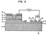
- Fig. 3shows a side view of a monolithically integrated circuit 30 consisting of a long wavelength (1.3-1.6 pm) laser and FET usefully made in accordance with the invention.
- the integrated circuit structureis made on a substrate of semi-insulating InP 31.
- the confinement layers 32 and 34surround the active layer 33 of a buried heterostructure laser typically made of InGaAsP with composition which lattice-matches to InP and emits at the desired frequency.
- An insulating layer 35is used to confine the current to a specific area and a metal contact layer 36 is used as the metal contact to the laser.
- the laseris driven by a FET circuit consisting of a channel layer 37 (usually InGaAs lattice-matched to InP), a drain contact 38 and source contact 39.
- the gate electrode 40is formed on a GaAs layer 41.
Landscapes
- Junction Field-Effect Transistors (AREA)
- Semiconductor Lasers (AREA)
Description
- The invention refers to a semiconductor device comprising at least one semiconductor element of the type as defined in the preamble clause of Claim 1. Such an element is especially applicable in a field effect transistor.
- Rapid development in both communication technology and computer technology has led to the requirement for higher speed circuits, more sensitive circuits and higher gain circuits. Such requirements have arisen at the same time as the further development of integrated circuit technology in which high packing densities in integrated circuits have become highly desirable.
- Optical communication technology provides an illustrative example. Optical communication has been developing at a rapid rate during the last few years. High sensitivity in receivers is desirable because it increases the distance between repeaters and reduces the number of repeaters in a particular communication system. Also of importance in optical communication systems is high speed amplifiers which permit high bit rates to be transmitted. High speed amplifier systems are also of use in other types of circuits including logic circuits, memory circuits, analog switching, high-input-impedance amplifiers, integrated circuits, etc.
- One of the most promising compound semiconductors for high speed, high gain devices is indium gallium arsenide and related compounds such as indium gallium arsenide phosphide. This is due to the high mobility and peak electron velocity exhibited by the III-V compound semiconductors. A particular difficulty is in fabricating suitable devices to take advantage of these properties. For example, the low barrier heights impose a limitation on the usefulness of Schottky barrier gates for MESFETs with indium gallium arsenide channel layers, in particular with Ino.53 GaO.47. As channel layers. Various corrective measures can be used to improve the barrier height characteristics, but a reliable process to produce such devices with reproducible characteristics has not been found.
- A possible approach to this problem is to interpose a layer of insulator material or wide band-gap material between metal and channel layer to produce the required barrier height for the control gate. Attempts to use a thin layer (40 nm) of gallium arsenide as the barrier material resulted in unacceptably high reverse bias currents (see IEEE Electron Device Letters, Vol. EDL-6, No. 1, January 1985). Attempts to use a thick (400 nm) layer of GaAs between metal and channel layer, with a still thicker (500 nm) graded In0.53Ga0.47As to GaAs layer being intervened, did not succeed either. They resulted in much lower transconductance and much higher pinch-off voltages (see Electronic Letters, Vol. 20, No. 21, October 1984, pages 865 and 866).
- The invention is a semiconductor device comprising at least one semiconductor element, said element comprising a first epitaxial region comprising InP or III-V semiconductor compound approximately lattice-matched to InP, a gate electrode, a second epitaxial region essentially consisting of gallium arsenide and contacting both the first epitaxial region and the gate electrode, and a Schottky barrier formed between gate electrode and second epitaxial region, characterized in that said second epitaxial region has a thickness of from more than 70 nm to 300 nm so as to minimize the reverse gate leakage current.
- The second epitaxial region of the indicated thickness range serves as a barrier layer to insure low reverse leakage currents. Satisfactory results are obtained with barrier layer thicknesses of greater than 70 nm, but preferred thicknesses are greater than 80, 100 or even 150 nm. Thicknesses greater than 300 nm are wasteful of material and processing time. Also, dislocations are more likely to result from the lattice strain, and device characteristics depending on field penetration into the channel layer might not be optimum. Typical structures have indium gallium arsenide as the channel material and indium phosphide as the substrate material. Devices made in accordance with the invention have high speeds, high transconductance and are suitable for integration with optical indium phosphide devices (e.g., photodetectors, lasers, etc.).
- Fig. 1 shows a side view of a field effect transistor featuring a gallium arsenide barrier layer;
- Fig. 2 shows the reverse gate leakage current as a function of gate voltage for two structures with different barrier layer thicknesses; and
- Fig. 3 shows a side view of a monolithically integrated FET-laser structure.
- The invention is based on the discovery that gallium arsenide layers in a certain thickness range, when deposited on a mismatched layer such as InP or Ga0.47In0.53As, can yield very low gate leakage currents. Such layers are useful in a variety of semiconductor structures. These GaAs layers from Schottky barriers with reasonable barrier heights and low reverse-bias leakage currents. Such barrier structures are useful in a variety of semiconductor structures, particularly where the basic layer exhibits only low Schottky barrier heights. For example, it is useful for gate electrodes in field effect transistors where the substrate material is indium phosphide and the channel material is indium phosphide or a semiconductor lattice-matched to indim phosphide (e.g., indium gallium arsenide with approximate composition InO.53GaO.47As or indium aluminum arsenide with approximate composition Ino.s2Alo.aaAs). The gallium arsenide layers produce increased Schottky barrier heights which reduces the reverse bias current.
- In general terms, the invention involves use of gallium arsenide in a certain thickness range as a lattice-mismatched layer on indium gallium arsenide to produce a Schottky barrier with reasonable height. At present, the most significant applications of such a structural element is with field effect transistors. The preferred channel material is indium gallium arsenide, particularly the composition of indium gallium arsenide that is lattice-matched to indium phosphide. There are two reasons why indium gallium arsenide is an important channel material: first, it has high low- field electron mobility, and, second, it can be lattice-matched to indium phosphide useful for a variety of long-wavelength lightwave integrated circuits. Particularly useful are integrated detector circuits for lightwave receivers and laser driver circuits as well as arrays of FET circuits for fast memories and logic circuits.
- A typical
FET semiconductor structure 10 using the gallium arsenide layer is shown in Fig. 1. The structure is grown on a (100) oriented semi-insulating (usually iron-doped) indium phosphide substrate 11. Epitaxial layers are typically grown on this substrate by molecular beam epitaxy (MBE). The active device layers consists of: first, a 60 nm thick undoped Ga0.47ln0.53Assemi-insulating buffer layer 12; second, a 40 nm thick n-Ga0.47ln0.53Aslayer 13 doped with silicon to a concentration of 8x10¹⁶ atoms cm-3, a 96 nm thick n-GaAs layer 14 doped with silicon to a concentration of about 1016 atoms cm-3 and a n+GaAs layer 15 with thickness of about 34 nm and silicon doping concentration of about 1018 atomscm-3. - Various electrodes are also incorporated into the structure including a
source 16, drain 17 (both typically made of germanium-gold) and agate electrode 19 made of aluminum. Gate lengths were typically 1.411m and gate widths of about 240 pm. In various applications such as semiconductor devices and circuits, a plurality of FETs like that described above may be used, often mounted on the same substrate. Typical characteristics of the device are as follows: external transconductance gm=104 mS/mm at VDS=-3.5 volts adn VGS=-0.2 volts; source resistance of 15 ohms for 240 µm gate widths. - The intrinsic transconductance is given by the formula:

- To further characterize the quality of the mismatched GaAs layer and understand its effect on device performance, certain FET devices were fabricated on wafers with thin and thick GaAs layers and their reverse gate leakage currents compared. Ni/Ge/Au was used as source and drain ohmic contacts and AI was deposited as gate metal. Both samples have a gate dimension of 1.4 umx240 um. Fig. 2 shows the typical reverse gate leakage currents of both samples. Sample 1 has a thin GaAs layer of about 58 nm;
Sample 2 has a thick GaAs layer of about 130 nm. It is clear that the devices made on a thick GaAs layer have a leakage current at least two orders of magnitude smaller than those of the thin layered sample. For example, Sample 1 has a leakage current of 200 pA at 1 V bias whileSample 2 has a leakage current of only 480 nA. Although the effect of doping levels in the GaAs layer cannot be totally ruled out, the manor cause for the reduced leakage current in the thick sample is believed to be the reduction in dislocation densities at the surface where Schottky barriers are formed. In the case of the thin-layered sample where Schottky barriers were made on the surface of highly dislocated GaAs, currents can leak through dislocations. It is believed that further reduction in leakage currents can be achieved by improving crystal growth. - Fig. 3 shows a side view of a monolithically integrated
circuit 30 consisting of a long wavelength (1.3-1.6 pm) laser and FET usefully made in accordance with the invention. The integrated circuit structure is made on a substrate ofsemi-insulating InP 31. The confinement layers 32 and 34 surround theactive layer 33 of a buried heterostructure laser typically made of InGaAsP with composition which lattice-matches to InP and emits at the desired frequency. An insulatinglayer 35 is used to confine the current to a specific area and ametal contact layer 36 is used as the metal contact to the laser. The laser is driven by a FET circuit consisting of a channel layer 37 (usually InGaAs lattice-matched to InP), adrain contact 38 andsource contact 39. Thegate electrode 40 is formed on aGaAs layer 41. Such structures provide good integration, the possibility of mass production and reduced price together with excellent performance.

Claims (7)
Applications Claiming Priority (2)
| Application Number | Priority Date | Filing Date | Title |
|---|---|---|---|
| US745294 | 1985-06-14 | ||
| US06/745,294US4745447A (en) | 1985-06-14 | 1985-06-14 | Gallium arsenide on gallium indium arsenide Schottky barrier device |
Publications (3)
| Publication Number | Publication Date |
|---|---|
| EP0205164A2 EP0205164A2 (en) | 1986-12-17 |
| EP0205164A3 EP0205164A3 (en) | 1987-12-23 |
| EP0205164B1true EP0205164B1 (en) | 1990-05-16 |
Family
ID=24996087
Family Applications (1)
| Application Number | Title | Priority Date | Filing Date |
|---|---|---|---|
| EP86107956AExpiredEP0205164B1 (en) | 1985-06-14 | 1986-06-11 | Semiconductor device structure |
Country Status (5)
| Country | Link |
|---|---|
| US (1) | US4745447A (en) |
| EP (1) | EP0205164B1 (en) |
| JP (1) | JP2636840B2 (en) |
| CA (1) | CA1240406A (en) |
| DE (1) | DE3671328D1 (en) |
Families Citing this family (10)
| Publication number | Priority date | Publication date | Assignee | Title |
|---|---|---|---|---|
| JPS63114176A (en)* | 1986-10-31 | 1988-05-19 | Fujitsu Ltd | High-speed field effect semiconductor device |
| JPS63144580A (en)* | 1986-12-09 | 1988-06-16 | Nec Corp | Field-effect transistor |
| JPS63276267A (en)* | 1987-05-08 | 1988-11-14 | Fujitsu Ltd | Manufacturing method of semiconductor device |
| US5091759A (en)* | 1989-10-30 | 1992-02-25 | Texas Instruments Incorporated | Heterostructure field effect transistor |
| JPH0547798A (en)* | 1991-01-31 | 1993-02-26 | Texas Instr Inc <Ti> | Gaas fet with resistive a1gaas |
| US5298441A (en)* | 1991-06-03 | 1994-03-29 | Motorola, Inc. | Method of making high transconductance heterostructure field effect transistor |
| JPH0521468A (en)* | 1991-07-17 | 1993-01-29 | Sumitomo Electric Ind Ltd | Manufacture of field-effect transistor |
| JP3601649B2 (en)* | 1996-12-25 | 2004-12-15 | 株式会社村田製作所 | Field effect transistor |
| US6097748A (en)* | 1998-05-18 | 2000-08-01 | Motorola, Inc. | Vertical cavity surface emitting laser semiconductor chip with integrated drivers and photodetectors and method of fabrication |
| WO2017189124A1 (en)* | 2016-04-29 | 2017-11-02 | Stc. Unm | Wafer level gate modulation enhanced detectors |
Family Cites Families (10)
| Publication number | Priority date | Publication date | Assignee | Title |
|---|---|---|---|---|
| US3218205A (en)* | 1962-07-13 | 1965-11-16 | Monsanto Co | Use of hydrogen halide and hydrogen in separate streams as carrier gases in vapor deposition of iii-v compounds |
| FR2386903A1 (en)* | 1977-04-08 | 1978-11-03 | Thomson Csf | FIELD EFFECT TRANSISTOR ON LARGE BAND FORBIDDEN SUPPORT |
| GB2012480A (en)* | 1978-01-12 | 1979-07-25 | Plessey Co Ltd | Heterostructure field effect transistors |
| FR2465318A1 (en)* | 1979-09-10 | 1981-03-20 | Thomson Csf | FIELD EFFECT TRANSISTOR WITH HIGH BREAKAGE FREQUENCY |
| US4360246A (en)* | 1980-05-23 | 1982-11-23 | Hughes Aircraft Company | Integrated waveguide and FET detector |
| JPS58147166A (en)* | 1982-02-26 | 1983-09-01 | Fujitsu Ltd | Semiconductor device |
| JPS59222988A (en)* | 1983-06-01 | 1984-12-14 | Matsushita Electric Ind Co Ltd | Compound semiconductor device and its manufacturing method |
| JPS59222986A (en)* | 1983-06-01 | 1984-12-14 | Matsushita Electric Ind Co Ltd | Method for manufacturing compound semiconductor devices |
| JPS609174A (en)* | 1983-06-29 | 1985-01-18 | Fujitsu Ltd | semiconductor equipment |
| JPS61225874A (en)* | 1985-03-29 | 1986-10-07 | Sumitomo Electric Ind Ltd | field effect transistor |
- 1985
- 1985-06-14USUS06/745,294patent/US4745447A/ennot_activeExpired - Lifetime
- 1986
- 1986-05-28CACA000510185Apatent/CA1240406A/ennot_activeExpired
- 1986-06-11DEDE8686107956Tpatent/DE3671328D1/ennot_activeExpired - Fee Related
- 1986-06-11EPEP86107956Apatent/EP0205164B1/ennot_activeExpired
- 1986-06-13JPJP61136381Apatent/JP2636840B2/ennot_activeExpired - Lifetime
Also Published As
| Publication number | Publication date |
|---|---|
| DE3671328D1 (en) | 1990-06-21 |
| EP0205164A3 (en) | 1987-12-23 |
| CA1240406A (en) | 1988-08-09 |
| EP0205164A2 (en) | 1986-12-17 |
| JP2636840B2 (en) | 1997-07-30 |
| JPS61290776A (en) | 1986-12-20 |
| US4745447A (en) | 1988-05-17 |
Similar Documents
| Publication | Publication Date | Title |
|---|---|---|
| US5495115A (en) | Semiconductor crystalline laminate structure, forming method of the same, and semiconductor device employing the same | |
| US4829347A (en) | Process for making indium gallium arsenide devices | |
| US5329150A (en) | Semiconductor photodetector devices with pairs of monoatomic layers separated by intrinsic layers | |
| EP1210736B1 (en) | Method of forming a double recessed transistor | |
| US4882609A (en) | Semiconductor devices with at least one monoatomic layer of doping atoms | |
| US5091759A (en) | Heterostructure field effect transistor | |
| GB2285175A (en) | High electron mobility transistor | |
| EP0051271A1 (en) | Heterojunction semiconductor device | |
| US6242293B1 (en) | Process for fabricating double recess pseudomorphic high electron mobility transistor structures | |
| EP0205164B1 (en) | Semiconductor device structure | |
| JP2914049B2 (en) | Compound semiconductor substrate having heterojunction and field effect transistor using the same | |
| US4829346A (en) | Field-effect transistor and the same associated with an optical semiconductor device | |
| EP0080714A2 (en) | Hetero-junction semiconductor device | |
| US6787826B1 (en) | Heterostructure field effect transistor | |
| US4942438A (en) | Compound semiconductor field-effect transistor | |
| US4600932A (en) | Enhanced mobility buried channel transistor structure | |
| US5024967A (en) | Doping procedures for semiconductor devices | |
| US5466955A (en) | Field effect transistor having an improved transistor characteristic | |
| EP0258530A2 (en) | Photoreceiver | |
| Kuo et al. | New pseudomorphic MODFETs utilizing Ga 0.47-u In 0.53+ u As/Al 0.48+ u In 0.52-u As heterostructures | |
| US5311045A (en) | Field effect devices with ultra-short gates | |
| US6787821B2 (en) | Compound semiconductor device having a mesfet that raises the maximum mutual conductance and changes the mutual conductance | |
| US5408111A (en) | Field-effect transistor having a double pulse-doped structure | |
| US5216260A (en) | Optically bistable semiconductor device with pairs of monoatomic layers separated by intrinsic layers | |
| KR900007049B1 (en) | Field Effect Transistor |
Legal Events
| Date | Code | Title | Description |
|---|---|---|---|
| PUAI | Public reference made under article 153(3) epc to a published international application that has entered the european phase | Free format text:ORIGINAL CODE: 0009012 | |
| AK | Designated contracting states | Kind code of ref document:A2 Designated state(s):DE FR GB NL | |
| PUAL | Search report despatched | Free format text:ORIGINAL CODE: 0009013 | |
| AK | Designated contracting states | Kind code of ref document:A3 Designated state(s):DE FR GB NL | |
| 17P | Request for examination filed | Effective date:19880620 | |
| 17Q | First examination report despatched | Effective date:19880822 | |
| GRAA | (expected) grant | Free format text:ORIGINAL CODE: 0009210 | |
| AK | Designated contracting states | Kind code of ref document:B1 Designated state(s):DE FR GB NL | |
| REF | Corresponds to: | Ref document number:3671328 Country of ref document:DE Date of ref document:19900621 | |
| ET | Fr: translation filed | ||
| PLBE | No opposition filed within time limit | Free format text:ORIGINAL CODE: 0009261 | |
| STAA | Information on the status of an ep patent application or granted ep patent | Free format text:STATUS: NO OPPOSITION FILED WITHIN TIME LIMIT | |
| 26N | No opposition filed | ||
| PGFP | Annual fee paid to national office [announced via postgrant information from national office to epo] | Ref country code:GB Payment date:20010525 Year of fee payment:16 Ref country code:FR Payment date:20010525 Year of fee payment:16 | |
| PGFP | Annual fee paid to national office [announced via postgrant information from national office to epo] | Ref country code:NL Payment date:20010529 Year of fee payment:16 | |
| PGFP | Annual fee paid to national office [announced via postgrant information from national office to epo] | Ref country code:DE Payment date:20010629 Year of fee payment:16 | |
| REG | Reference to a national code | Ref country code:GB Ref legal event code:IF02 | |
| PG25 | Lapsed in a contracting state [announced via postgrant information from national office to epo] | Ref country code:GB Free format text:LAPSE BECAUSE OF NON-PAYMENT OF DUE FEES Effective date:20020611 | |
| PG25 | Lapsed in a contracting state [announced via postgrant information from national office to epo] | Ref country code:NL Free format text:LAPSE BECAUSE OF NON-PAYMENT OF DUE FEES Effective date:20030101 Ref country code:DE Free format text:LAPSE BECAUSE OF NON-PAYMENT OF DUE FEES Effective date:20030101 | |
| GBPC | Gb: european patent ceased through non-payment of renewal fee | Effective date:20020611 | |
| PG25 | Lapsed in a contracting state [announced via postgrant information from national office to epo] | Ref country code:FR Free format text:LAPSE BECAUSE OF NON-PAYMENT OF DUE FEES Effective date:20030228 | |
| NLV4 | Nl: lapsed or anulled due to non-payment of the annual fee | Effective date:20030101 | |
| REG | Reference to a national code | Ref country code:FR Ref legal event code:ST |