EP0200863A1 - Semiconductor device with structures of thyristors and diodes - Google Patents
Semiconductor device with structures of thyristors and diodesDownload PDFInfo
- Publication number
- EP0200863A1 EP0200863A1EP86102558AEP86102558AEP0200863A1EP 0200863 A1EP0200863 A1EP 0200863A1EP 86102558 AEP86102558 AEP 86102558AEP 86102558 AEP86102558 AEP 86102558AEP 0200863 A1EP0200863 A1EP 0200863A1
- Authority
- EP
- European Patent Office
- Prior art keywords
- zone
- protection zone
- semiconductor component
- thyristor
- gto
- Prior art date
- Legal status (The legal status is an assumption and is not a legal conclusion. Google has not performed a legal analysis and makes no representation as to the accuracy of the status listed.)
- Granted
Links
- 239000004065semiconductorSubstances0.000titleclaimsdescription34
- 230000001681protective effectEffects0.000claimsabstractdescription22
- 239000002800charge carrierSubstances0.000claimsabstractdescription19
- 238000002161passivationMethods0.000claimsdescription14
- 239000004642PolyimideSubstances0.000claimsdescription2
- 230000036961partial effectEffects0.000claimsdescription2
- 229920001721polyimidePolymers0.000claimsdescription2
- 238000010893electron trapMethods0.000claims2
- 230000007547defectEffects0.000claims1
- 230000002441reversible effectEffects0.000abstractdescription5
- 238000000034methodMethods0.000description10
- 230000008569processEffects0.000description9
- 239000000370acceptorSubstances0.000description7
- 238000005530etchingMethods0.000description7
- 230000003071parasitic effectEffects0.000description5
- 238000013461designMethods0.000description4
- BASFCYQUMIYNBI-UHFFFAOYSA-NplatinumChemical compound[Pt]BASFCYQUMIYNBI-UHFFFAOYSA-N0.000description4
- XUIMIQQOPSSXEZ-UHFFFAOYSA-NSiliconChemical compound[Si]XUIMIQQOPSSXEZ-UHFFFAOYSA-N0.000description3
- 229910052710siliconInorganic materials0.000description3
- 239000010703siliconSubstances0.000description3
- 229910052782aluminiumInorganic materials0.000description2
- XAGFODPZIPBFFR-UHFFFAOYSA-NaluminiumChemical compound[Al]XAGFODPZIPBFFR-UHFFFAOYSA-N0.000description2
- 230000000903blocking effectEffects0.000description2
- 238000009792diffusion processMethods0.000description2
- 230000000694effectsEffects0.000description2
- 239000000463materialSubstances0.000description2
- 229910052751metalInorganic materials0.000description2
- 239000002184metalSubstances0.000description2
- 229910052697platinumInorganic materials0.000description2
- 230000009467reductionEffects0.000description2
- 238000012549trainingMethods0.000description2
- 230000007704transitionEffects0.000description2
- ZOXJGFHDIHLPTG-UHFFFAOYSA-NBoronChemical compound[B]ZOXJGFHDIHLPTG-UHFFFAOYSA-N0.000description1
- GYHNNYVSQQEPJS-UHFFFAOYSA-NGalliumChemical compound[Ga]GYHNNYVSQQEPJS-UHFFFAOYSA-N0.000description1
- ZOKXTWBITQBERF-UHFFFAOYSA-NMolybdenumChemical compound[Mo]ZOKXTWBITQBERF-UHFFFAOYSA-N0.000description1
- 230000008901benefitEffects0.000description1
- 229910052796boronInorganic materials0.000description1
- 230000015556catabolic processEffects0.000description1
- 230000008859changeEffects0.000description1
- 230000006378damageEffects0.000description1
- 238000012217deletionMethods0.000description1
- 230000037430deletionEffects0.000description1
- 230000005684electric fieldEffects0.000description1
- 230000006870functionEffects0.000description1
- 229910052733galliumInorganic materials0.000description1
- PCHJSUWPFVWCPO-UHFFFAOYSA-NgoldChemical compound[Au]PCHJSUWPFVWCPO-UHFFFAOYSA-N0.000description1
- 229910052737goldInorganic materials0.000description1
- 239000010931goldSubstances0.000description1
- 229910001385heavy metalInorganic materials0.000description1
- 230000006872improvementEffects0.000description1
- 230000001939inductive effectEffects0.000description1
- 238000002347injectionMethods0.000description1
- 239000007924injectionSubstances0.000description1
- 238000009434installationMethods0.000description1
- 230000000873masking effectEffects0.000description1
- 150000002739metalsChemical class0.000description1
- 229910052750molybdenumInorganic materials0.000description1
- 239000011733molybdenumSubstances0.000description1
- 230000009993protective functionEffects0.000description1
- 230000005855radiationEffects0.000description1
- 230000002829reductive effectEffects0.000description1
- 238000012552reviewMethods0.000description1
- 238000005496temperingMethods0.000description1
Images

Classifications
- H—ELECTRICITY
- H10—SEMICONDUCTOR DEVICES; ELECTRIC SOLID-STATE DEVICES NOT OTHERWISE PROVIDED FOR
- H10D—INORGANIC ELECTRIC SEMICONDUCTOR DEVICES
- H10D84/00—Integrated devices formed in or on semiconductor substrates that comprise only semiconducting layers, e.g. on Si wafers or on GaAs-on-Si wafers
- H10D84/101—Integrated devices comprising main components and built-in components, e.g. IGBT having built-in freewheel diode
- H10D84/131—Thyristors having built-in components
- H10D84/135—Thyristors having built-in components the built-in components being diodes
- H10D84/136—Thyristors having built-in components the built-in components being diodes in anti-parallel configurations, e.g. reverse current thyristor [RCT]
- H—ELECTRICITY
- H10—SEMICONDUCTOR DEVICES; ELECTRIC SOLID-STATE DEVICES NOT OTHERWISE PROVIDED FOR
- H10D—INORGANIC ELECTRIC SEMICONDUCTOR DEVICES
- H10D62/00—Semiconductor bodies, or regions thereof, of devices having potential barriers
- H10D62/10—Shapes, relative sizes or dispositions of the regions of the semiconductor bodies; Shapes of the semiconductor bodies
- H10D62/13—Semiconductor regions connected to electrodes carrying current to be rectified, amplified or switched, e.g. source or drain regions
- H10D62/141—Anode or cathode regions of thyristors; Collector or emitter regions of gated bipolar-mode devices, e.g. of IGBTs
- H10D62/142—Anode regions of thyristors or collector regions of gated bipolar-mode devices
Definitions
- the inventionis based on a semiconductor component according to the preamble of patent claim 1.
- the inventionrelates to a prior art, as described in CH-PS 594 989.
- a reverse conducting thyristorspecified, which combines a thyristor and an anti-parallel diode on a silicon wafer.
- the mutual influence of the two componentsis avoided by special protective rings in the component.
- Such reverse-conducting thyristorsare used in power electronics for DC controllers, converters, uninterruptible power supply systems, electrostatic filters, etc., cf. the Swiss company magazine Brown Boveri Mitteilungen 1 (1979), pp. 5 -10.
- an inductive loade.g. B. a motor in the field of traction is controlled
- a current path in the opposite direction to the forward direction of the thyristoris to be provided.
- conventional thyristors in positively commutated circuitsrequire a commutation circuit for switching off.
- GTO thyristorsare available in a very wide range of breaking currents (20 A ...> 2000 A) and voltages (600 V ...> 4500 V), vgL IEEE Transaction on Electron Devices, Vol. ED-31, No. 12, Dec. 1984, pp. 1681-1686.
- the inventionsolves the problem of combining a GTO thyristor with an antiparallel diode in one component and decoupling the control current of the GTO thyristor as well as possible from the diode.
- An advantage of the inventionis that it results in lower costs for the user.
- the cost of an integrated elementis less than that of the thyristor and diode separately. Installation costs for a separate diode are eliminated. Decoupling the GTO thyristor and diode prevents a cathode short circuit. At the same time, it is ensured that only a few free charge carriers reach the region of the GTO thyristor during the conducting phase of the diode, so that misfires which could lead to destruction of the component are avoided.
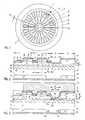
- the circular semiconductor waferwhich is not shown to scale in FIG. 1, has a GTO control electrode 7 in the center surrounded by an inert, electrically insulating passivation layer 6 which can withstand a high electric field strength.
- Polyimideis used as the passivation material.
- the length 1 of the GTO cathode electrodes 8 and 8 'is in the range from 2 mm ... 8 mm, their width m in the range from 100 ⁇ m ... 500 ⁇ m, preferably in the range from 200 ⁇ m ... 400 ⁇ m.
- the mean distance t in the circumferential direction of adjacent GTO cathode electrodes 8 and 8 'is in the range from 0.3 mm ... 0.5 mm.
- the radial distance r between the GTO cathode electrodes 8 and 8 ', cf. Fig. 2is in the range of 100 ⁇ m ... 1 mm, preferably in the range of 300 ⁇ m ... 500 ⁇ m.
- An electrode 9 of a diode anodeis located along the outer circumference of the semiconductor wafer. Between the electrode 9 and the area of the GTO thyristor there is a protection zone S of width s of typically at least two carrier diffusion lengths. This width s is to be chosen so large that only a small number of free charge carriers reach the region of the GTO thyristor during the conducting phase of the diode D.
- the radial distance of the GTO cathode electrodes 8 'from the protective zone Sis in the range from 10 ⁇ m ... 1 mm, preferably in the range from 100 ⁇ m ... 300 ⁇ m.
- the semiconductor waferhas a diameter, depending on the required maximum breaking current, in the range from 10 mm ... 100 mm and a thickness, depending on the required blocking voltage, in the range from 200 ⁇ m ... 1.5 mm.
- the cross section shown schematically in FIG. 2 along the line A in FIG. 1 from the center of the semiconductor wafer to its right edgeshows in the left part a region designated by GTO of two thyristors that can be switched off, called GTO region for short, which extends over the protection zone S is connected to the diode area D in the right part.
- the GTO areahas 4 charge carrier layers of alternating conductivity types n and p for each thyristor, namely for each thyristor a separate highly doped n-type emitter layer or an n + emitter layer 1 or 1 'as GTO cathode layer with a donor concentration at the Surface in the range of 10 19 cm- 3 ... 10 21 cm- 3 , a medium-doped p-type p-base layer 2 common to both thyristors with an acceptor concentration on the surface in the range of 10 "cm- 3 ...
- a first pn junction between the n + emitter layer 1, 1 'and the p base layer 2is denoted by 16, a second pn junction between the p base layer 2 and the n base layer 3 by 17 and a third pn Transition between the n - base layer 3 and the p + emitter layer 4 with 18.
- a space charge zone on both sides of the second pn transition 17is denoted by 5.
- 7denotes a control electrode which is recessed with respect to the n + emitter layers 1 and 1 'and which surrounds the GTO cathode electrodes 8 and 8' at a distance.
- the surface 19 of the control electrode region covered and contacted by the control electrode layer 7is lower than the first pn junction 16.
- the p-base layer 2 and the n-base layer 3extend from the thyristor region GTO via the protection zone S into the diode region D.
- the p-base layer 2there forms the anode of the diode D, which carries an electrode layer 9, which is at the same height the GTO cathode electrodes 8 and 8 '.
- the n - base layer 3borders in the diode region D on a highly doped n-type n + - diode layer, which forms the diode cathode.
- Both the p + emitter layer 4 of the GTO and the n - base layer 3 in the region of the protection zone S and the n + - diode layer 11have the same level on their outer surface and are common to all metal layers 10, which are a first main electrode of the semiconductor component forms, electrically contacted.
- All electrodes or electrode layersare made of aluminum. Of course, other metals such as gold, platinum, etc. are also suitable for electrical contacting.
- the passivation layer 6is applied between the GTO control electrode layer 7 and the GTO cathode electrodes 8 and 8 ′ and the electrode 9 of the diode anode.
- This passivation layer 6can cover the control electrode layer 7, except for a central area provided for the electrical connection, but not the GTO cathode electrodes 8 and 8 'and the electrode 9, since otherwise their electrical contacting with a molybdenum layer serving as the second main electrode 13, cf. Fig. 2, would not be guaranteed.
- the passivation layer 6can be at a small distance from the GTO cathode electrodes 8 and 8 ′ and from the electrode 9. A passivation of the surface 20 in the area of the protection zone is in principle not necessary.
- the greatest depth a of the recess in the protective zone S from the surface of the GTO cathode layer 1 and 1 'is in the range from 10 .mu.m ... 100 .mu.m.
- the surface 20 of the protection zone area Sis somewhat lower than the surface 19 of the adjacent control electrode area.
- the space charge zone 5is at a distance c from the surface 20 in the range from 1 ⁇ m to 30 ⁇ m, preferably from 1 ⁇ m to 10 ⁇ m, so that it does not reach this surface 20 at any point in the protection zone S.
- the charge carrier life in the diodeis preferably set to be shorter than in the thyristor.
- a p + protective ring 14 and an n + protective ring 15can be attached in the area of the protective zone S at a short distance adjacent to the n + diode layer 11 and preferably also to the p + emitter layer 4 3, see there. It is important that the width s of the protection zone S and the depth a of the recess in the protection zone S produced by etching are so large that an undesirable current component from the control electrode layer 7 to the diode anode remains negligibly small during the ignition and extinguishing process of the GTO thyristor .
- a further improvement in the decoupling of diode D and GTO thyristoris achieved by the semiconductor component partially shown in cross section in FIG. 3.
- the space charge zone 5is guided along a partial width x of the protection zone S up to its surface 20, the distance d of the undisturbed space charge zone 5 from the surface of the GTO cathode layer 1 and 1 ′ or from the surface of a p + - diode layer 12 being smaller is the maximum depth a of the recess in the protection zone S.
- the difference a -dis in the range from 1 ⁇ m to -30 ⁇ m, preferably in the range from 1 ⁇ m to -10 ⁇ m S.
- the deeper recess in the area of the protection zone S compared to FIG. 2is preferably produced by etching after the last high-temperature treatment of the semiconductor component.
- the second pn junction 17is located sufficiently far below the lowest surface 20 of the protection zone area so that the field strength E o below this surface 20 is ⁇ 105 V / cm, preferably ⁇ 2 ⁇ 10 4 V / cm.
- the second pn junction 17is guided in the area of the protection zone S at its lowest surface 20.
- This surface 20is deeper than the surface 19 of the control electrode region by an additional depth or by a distance e in the range from 1 ⁇ m to 50 ⁇ m, preferably in the range from 1 ⁇ m to 20 ⁇ m.
- This configuration of the semiconductor componentis achieved by homogeneously introducing acceptors such as boron, aluminum or gallium into the upper region of the silicon wafer, which is later to produce the p-type base layer 2. Then the p-type base layer 2 is removed over the section x of the protection zone S, for example by etching. Then it is tempered. During tempering, the acceptors of the p-base layer are thermally diffused, as a result of which the desired depth of the pn junction 17 is set. Since the acceptors have been removed in the area of the recess of the protection zone S, the second pn junction 17 and the space charge zone 5 at the edge of the protection zone bulge upwards.
- acceptorssuch as boron, aluminum or gallium
- etchingreduces the surface in the control region of the GTO thyristor and preferably also in the protective zone by at least the thickness of the n + emitter layer 1 or 1 ′ to the height of the surface 19.
- a parasitic control electrode currentis blocked during the ignition process; during the extinguishing process, the protection zone S acts like a lateral pnp transistor without a base current, which blocks a parasitic control electrode current.
- the protection zone Sacts like a lateral pnp transistor without a base current, which blocks a parasitic control electrode current.
- the p + emitter layer in the control electrode regionis interrupted by n + anode short-circuit zones 15 ', which make it easier to switch off the thyristor.
- the design of the semiconductor component according to FIG. 5differs from that of FIG. 4 in that the surface 19 in the control electrode area is at the same height as the surface 20 in the protection zone S and the second pn junction 17 and the space charge zone 5 are more deformed in the area of the protection zone. This is achieved by introducing acceptors into the p-base layer 2 masked in the area of the protection zone S and eliminating the first etching process.
- n s base layer 23with a donor concentration in the range of 10 "cm -3 ... 10" cm- 'is provided below the n base layer 3.
- the second pn junction 17 and the space charge zone 5are guided at a first and a second protection zone contact point 21 and 22 each having the same width b on the deepest surface 20 thereof.
- the width bdepends on the lateral diffusion, it is in the range up to 300 ⁇ m, preferably in the range up to 100 ⁇ m.
- the structure of the diode structurecorresponds to that of FIG. 3.
- the n + anode short-circuit zone 15 'in the central region of the semiconductor componentis widened compared to that according to FIG. 6 and extends over the diameter of the central part of the control electrode 7.
- the design of the semiconductor component according to FIG. 7differs from that according to FIG. 6 in that the surface 19 in the control electrode area is at the same height as the surface 20 in the protection zone S. This is achieved again, as in the embodiment according to FIG. 5, by masking the acceptors into the p-base layer 2 and omitting the first etching process.
- the protection zonecorresponds to several lateral pnp transistors connected in series without a base current, which block a parasitic control electrode current. It is advantageous that the protection zone width s 5 1 mm can be kept, so that only a small amount of semiconductor area is lost for conducting an electrical current.
- the field strength E o10 4 V / cm remains in the area of the protection zone, ie the requirements for the passivation layer 6 are modest.
- a reduction of the blocking voltage of only approx. 10%can be achieved. This can be desirable, since it achieves a targeted voltage breakdown under the surface, which corresponds to an integrated protective function and thus increased robustness.
- diode region Dinstead of the diode region D, several of them can be provided on the same semiconductor component. Instead of the two circular zones with GTO thyristors shown in FIG. 1, three or more circular ring zones with GTO thyristors can also be provided.
- the semiconductor bodycan have a square or other shape.
- the protection zone Scan additionally have cutouts or trenches. It is important that the thyristor and diode regions are well decoupled from one another, so that only a few charge carriers can change over to the other regions.
Landscapes
- Thyristors (AREA)
Abstract
Translated fromGermanDescription
Translated fromGermanBei der Erfindung wird ausgegangen von einem Halbleiterbauelement nach dem Oberbegriff des Patentanspruchs 1.The invention is based on a semiconductor component according to the preamble of
Mit diesem Oberbegriff nimmt die Erfindung auf einen Stand der Technik Bezug, wie er in der CH-PS 594 989 beschrieben ist. Dort ist ein rückwärtsleitender Thyristor angegeben, der einen Thyristor und eine antiparallele Diode auf einer Siliziumscheibe vereinigt. Die gegenseitige Beeinflussung der beiden Komponenten wird durch spezielle Schutzringe im Bauelement vermieden.With this preamble, the invention relates to a prior art, as described in CH-PS 594 989. There is a reverse conducting thyristor specified, which combines a thyristor and an anti-parallel diode on a silicon wafer. The mutual influence of the two components is avoided by special protective rings in the component.
Derartige rückwärtsleitende Thyristoren werden in der Leistungselektronik für Gleichstromsteller, Umrichter, unterbrechungsfreie Stromversorgungsaniagen, Elektrofilter usw. verwendet, vgl. die Schweizer Firmenzeitschrift Brown Boveri Mitteilungen 1 (1979), S. 5 -10. In allen Fällen, in denen eine induktive Last, z. B. ein Motor auf dem Gebiet der Traktion, angesteuert wird, ist ein Strompfad in Gegenrichtung zur Durchlassrichtung des Thyristors vorzusehen. Nachteilig dabei ist, dass konventionelle Thyristoren in zwangskommutierten Schaltungen zum Abschalten eine Kommutierungsschaltung erfordern.Such reverse-conducting thyristors are used in power electronics for DC controllers, converters, uninterruptible power supply systems, electrostatic filters, etc., cf. the Swiss company magazine Brown Boveri Mitteilungen 1 (1979), pp. 5 -10. In all cases where an inductive load, e.g. B. a motor in the field of traction is controlled, a current path in the opposite direction to the forward direction of the thyristor is to be provided. The disadvantage here is that conventional thyristors in positively commutated circuits require a commutation circuit for switching off.
Aus Hitachi Review, Vol. 31 (1982) No. 1, S. 23 -27 ist es bekannt, ausschaltbare, d.h. GTO (Gate Tum-O ff)-Thyristoren anstelle der konventionellen Thyristoren einzusetzen.From Hitachi Review, Vol. 31 (1982) No. 1, pp. 23-27 it is known to be switchable, i.e. Use GTO (Gate Tum-O ff) thyristors instead of conventional thyristors.
GTO-Thyristoren sind in einem sehr breiten Bereich von Ausschaltströmen (20 A ... > 2000 A) und Spannungen (600 V ... > 4500 V) erhältlich, vgL IEEE Transaction on Electron Devices, Vol. ED-31, No. 12, Dez. 1984, S. 1681 -1686.GTO thyristors are available in a very wide range of breaking currents (20 A ...> 2000 A) and voltages (600 V ...> 4500 V), vgL IEEE Transaction on Electron Devices, Vol. ED-31, No. 12, Dec. 1984, pp. 1681-1686.
Wird ein GTO-Thyristor antiparallel zu einer separaten Diode geschaltet, so treten folgende Probleme auf:
- -die Streuinduktivität des äusseren Kreises führt zu Ueberspannungen, die für den GTO-Thyristor - schädlich sein können,
- -die Diode muss hinsichtlich ihrer Kenndaten an den GTO-Thyristor angepasst sein, was nur in wenigen Fällen garantiert werden kann,
- the leakage inductance of the outer circuit leads to overvoltages which can be harmful to the GTO thyristor,
- -The characteristics of the diode must be adapted to the GTO thyristor, which can only be guaranteed in a few cases.
Die Erfindung, wie sie im Patentanspruch 1 und 6 definiert ist, löst die Aufgabe, einen GTO-Thyristor mit einer antiparallelen Diode in einem Bauelement zu vereinigen und den Steuerstrom des GTO-Thyristors möglichst gut von der Diode zu entkoppeln.The invention, as defined in
Ein Vorteil der Erfindung besteht darin, dass für den Anwender geringere Kosten resultieren. Die Kosten für ein integriertes Element sind geringer als jene für Thyristor und Diode separat. Montagekosten für eine separate Diode entfallen. Durch die Entkopplung von GTO-Thyristor und Diode wird ein Kathodenkurzschluss vermieden. Gleichzeitig wird gewährleistet, dass während der Leitphase der Diode nur wenige freie Ladungsträger in den Bereich des GTO-Thyristors gelangen, so dass dort Fehlzündungen, die zu einer Zerstörung des Bauelements führen könnten, vermieden werden.An advantage of the invention is that it results in lower costs for the user. The cost of an integrated element is less than that of the thyristor and diode separately. Installation costs for a separate diode are eliminated. Decoupling the GTO thyristor and diode prevents a cathode short circuit. At the same time, it is ensured that only a few free charge carriers reach the region of the GTO thyristor during the conducting phase of the diode, so that misfires which could lead to destruction of the component are avoided.
Die Erfindung wird nachstehend anhand von Ausführungsbeispielen erläutert. Es zeigen:
- Fig. 1 ein scheibenförmiges, rotationssymmetrisches Halbleiterbauelement in Draufsicht,
- Fig. 2 einen Querschnitt durch einen Teil des Halbleiterbauelements gemäss Fig. 1 längs der Linie A,
- Fig. 3, 4, 6 Querschnitte durch Teile von Halbleiterbauelementen in speziellen Ausbildungen,
- Fig. 5 und 7 spezielle Ausbildungen einer Schutzzone zwischen Diode und GTO-Thyristor gemäss Fig. 4 bzw. 6.
- 1 shows a disk-shaped, rotationally symmetrical semiconductor component in plan view,
- 2 shows a cross section through part of the semiconductor component according to FIG. 1 along line A,
- 3, 4, 6 cross sections through parts of semiconductor components in special designs,
- 5 and 7 special designs of a protection zone between the diode and GTO thyristor according to FIGS. 4 and 6.
In den Figuren sind gleiche Teile mit gleichen Bezugszeichen gekennzeichnet.In the figures, the same parts are identified by the same reference numerals.
Die in Fig. 1 nicht massstabsgerecht dargestellte, kreisförmige Halbleiterscheibe weist im Zentrum eine GTO-Steuerelektrode 7 umgeben von einer inerten, elektrisch isolierenden Passivierungsschicht 6 auf, die eine hohe elektrische Feldstärke aushält. Als Passivierungsmaterial wird Polyimid verwendet. Aus dieser Passivierungsschicht 6 ragen in zwei konzentrischen Zonen inselartig zahlreiche längliche GTO-Kathodeneiektroden 8 und 8' heraus. Die Länge 1 der GTO-Kathodenelekiroden 8 und 8' liegt im Bereich von 2 mm ... 8 mm, deren Breite m im Bereich von 100 um ... 500 µm, vorzugsweise im Bereich von 200 µm ... 400 µm. Der mittlere Abstand t in Kreisumfangsrichtung benachbarter GTO-Kathodenelektroden 8 bzw. 8' liegt im Bereich von 0,3 mm ... 0,5 mm. Der radiale Abstand r zwischen den GTO-Kathodenelektroden 8 und 8', vgl. Fig. 2, liegt im Bereich von 100 u.m ... 1 mm, vorzugsweise im Bereich von 300 um ... 500 um.The circular semiconductor wafer, which is not shown to scale in FIG. 1, has a
Längs des Aussenumfangs der Halbleiterscheibe befindet sich eine Elektrode 9 einer Dioden-Anode. Zwischen der Elektrode 9 und dem Bereich des GTO-Thyristors befindet sich eine Schutzzone S der Breite s von typischerweise mindestens zwei Trägerdiffusionslängen. Diese Breite s ist so gross zu wählen, dass während der Leitphase der Diode D nur eine geringe Zahl freier Ladungsträger in den Bereich des GTO-Thyristors gelangen. Der radiale Abstand der GTO-Kathodenelektroden 8' von der Schutzzone S liegt im Bereich von 10 um ... 1 mm, vorzugsweise im Bereich von 100 um ... 300 um.An
Die Halbleiterscheibe hat einen Durchmesser, je nach der geforderten maximalen Ausschaltstromstärke, im Bereich von 10 mm ... 100 mm und eine Dicke, je nach geforderter Sperrspannung, im Bereich von 200 um ... 1,5 mm.The semiconductor wafer has a diameter, depending on the required maximum breaking current, in the range from 10 mm ... 100 mm and a thickness, depending on the required blocking voltage, in the range from 200 µm ... 1.5 mm.
Der in Fig. 2 schematisch dargestellte Querschnitt längs der Linie A in Fig. 1 von der Mitte der Halbleiterscheibe bis zu deren rechtem Rand zeigt im linken Teil einen mit GTO bezeichneten Bereich zweier ausschaltbarer Thyristoren, kurz GTO-Bereich genannt, der über die Schutzzone S mit dem Diodenbereich D im rechten Teil in Verbindung steht.The cross section shown schematically in FIG. 2 along the line A in FIG. 1 from the center of the semiconductor wafer to its right edge shows in the left part a region designated by GTO of two thyristors that can be switched off, called GTO region for short, which extends over the protection zone S is connected to the diode area D in the right part.
Der GTO-Bereich weist für jeden Thyristor 4 Ladungsträger schichten abwechselnden Leitungstyps n und p auf, und zwar für jeden Thyristor eine separate hochdotierte n-leitende Emitterschicht bzw. eine n+-Emitterschicht 1 bzw. 1' als GTO-Kathodenschicht mit einer Donatorenkonzentration an der Oberfläche im Bereich von 1019 cm-3 ... 1021 cm-3, eine für beide Thyristoren gemeinsame mitteldotierte p-leitende p-Basisschicht 2 mit einer Akzeptorenkonzentration an der Oberfläche im Bereich von 10" cm-3 ... 10" cm-3, eine für beide Thyristoren gemeinsame niedrigdotierte, n-leitende n--Basisschicht 3 mit einer Donatorenkonzentration im Bereich von 1013cm-3 ... 1015cm-3 und eine gemeinsame hochdotierte, p-leitende p+- Emitterschicht 4 als GTO-Anodenschicht mit einer Akzeptorenkonzentration im Bereich von 1018 cm-' ... 1020 cm-' an der Oberfläche.The GTO area has 4 charge carrier layers of alternating conductivity types n and p for each thyristor, namely for each thyristor a separate highly doped n-type emitter layer or an n +
Ein erster pn-Uebergang zwischen der n+- Emitterschicht 1, 1' und der p-Basisschicht 2 ist mit 16 bezeichnet, ein zweiter pn-Uebergang zwischen der p-Basisschicht 2 und der n--Basisschicht 3 mit 17 und ein dritter pn-Uebergang zwischen der n--Basisschicht 3 und der p+-Emitterschicht 4 mit 18. Eine Raumladungszone zu beiden Seiten des zweiten pn-Uebergangs 17 ist mit 5 bezeichnet. Mit 7 ist eine bezüglich der n+-Emitter- schichten 1 und 1' vertieft liegende Steuerelektrode bezeichnet, welche mit Abstand die GTO-Kathodenelektroden 8 und 8' umgibt. Die Oberfläche 19 des von der Steuerelektrodenschicht 7 überdeckten und kontaktierten Steuerelektrodenbereiches liegt tiefer als der erste pn-Uebergang 16.A first pn junction between the n+ emitter layer 1, 1 'and the
Die p-Basisschicht 2 und die n--Basisschicht 3 erstrecken sich vom Thyristorbereich GTO über die Schutzzone S in den Diodenbereich D. Die p-Basisschicht 2 bildet dort die Anode der Diode D, welche eine Elektrodenschicht 9 trägt, die auf gleicher Höhe mit den GTO-Kathodenelek troden 8 und 8' liegt. Die n--Basisschicht 3 grenzt im Diodenbereich D an eine hochdotierte n-leitende n+- Diodenschicht, welche die Diodenkathode bildet. Sowohl die p+-Emitterschicht 4 des GTO als auch die n--Basisschicht 3 im Bereich der Schutzzone S und die n+-Diodenschicht 11 weisen an ihrer Aussenfläche gleiches Niveau auf und sind durch eine allen gemeinsame Metallschicht 10, welche eine erste Hauptelektrode des Halbleiterbauelements bildet, elektrisch kontaktiert.The p-
Alle Elektroden bzw. Elektrodenschichten bestehen aus Aluminium. Selbstverständlich sind zur elektrischen Kontaktierung auch andere Metalle wie Gold, Platin, usw. geeignet.All electrodes or electrode layers are made of aluminum. Of course, other metals such as gold, platinum, etc. are also suitable for electrical contacting.
Zwischen der GTO-Steuerelektrodenschicht 7 und den GTO-Kathodenelektroden 8 und 8' sowie der Elektrode 9 der Dioden-Anode ist die Passivierungsschicht 6 aufgebracht. Diese Passivierungsschicht 6 kann die Steuerelektrodenschicht 7, bis auf einen zentralen, für den elektrischen Anschluss vorgesehenen Bereich, überdecken, nicht jedoch die GTO-Kathodenelektroden 8 und 8' sowie die Elektrode 9, da sonst deren gemeinsame elektrische Kontaktierung mit einer als zweite Hauptelektrode dienenden Molybdänschicht 13, vgl. Fig. 2, nicht garantiert wäre. Die Passivierungsschicht 6 kann sicherheitshalber zu den GTO-Kathodenelektroden 8 und 8' sowie zu der Elektrode 9 einen kleinen Abstand aufweisen. Eine Passivierung der Oberfläche 20 im Bereich der Schutzzone ist im Prinzip nicht erforderlich.The
Die grösste Tiefe a der Aussparung der Schutzzone S von der Oberfläche der GTO-Kathodenschicht 1 und 1' liegt im Bereich von 10 um ... 100 um. Die Oberfläche 20 des Schutzzonenbereiches S liegt etwas tiefer als die Oberfläche 19 des angrenzenden Steuerelektrodenbereiches. Die Raumladungszone 5 hat von der Oberfläche 20 einen Abstand c im Bereich von 1 um ... 30 µm, vorzugsweise von 1 um ... 10 um, so dass sie an keinem Punkt der Schutzzone S diese Oberfläche 20 erreicht.The greatest depth a of the recess in the protective zone S from the surface of the
Durch Einbau von Schwermetallatomen wie Geld oder Platin in das Siliziumgrundmaterial des Halbleiterbauelements oder durch Elektronen-oder Gammabestrahlung ist die Ladungsträgerlebensdauer in der Diode vorzugsweise kürzer eingestellt als im Thyristor.By incorporating heavy metal atoms such as money or platinum in the silicon base material of the semiconductor component or by electron or gamma radiation, the charge carrier life in the diode is preferably set to be shorter than in the thyristor.
Zur besseren Entkopplung von Diode D und Thyristor GTO können im Bereich der Schutzzone S mit geringem Abstand angrenzend an die n+- Diodenschicht 11 und vorzugsweise auch an die p+-Emitterschicht 4 ein p+-Schutzring 14 und ein n+-Schutzring 15 angebracht sein, wie bei der Ausgestaltung gemäss Fig. 3, siehe dort. Wichtig ist, dass die Breite s der Schutzzone S und die durch Aetzen erzeugte Tiefe a der Aussparung der Schutzzone S so gross sind, dass ein unerwünschter Stromanteil von der Steuerelektrodenschicht 7 zur Dioden-Anode beim Zünd-und Löschvorgang des GTO-Thyristors vemachlässigbar klein bleibt.For better decoupling of diode D and thyristor GTO, a p+
Eine weitere Verbesserung der Entkopplung von Diode D und GTO-Thyristor wird durch das in Fig. 3 im Querschnitt teilweise dargestellte Halbleiterbauelement erreicht. Hier ist die Raumladungszone 5 längs einer Teilbreite x der Schutzzone S bis an deren Oberfläche 20 geführt, wobei der Abstand d der ungestörten Raumladungszone 5 von der Oberfläche der GTO-Kathodenschicht 1 und 1' bzw. von der Oberfläche einer p+-Diodenschicht 12 kleiner ist als die maximale Tiefe a der Aussparung der Schutz zone S. Die Differenz a -d liegt im Bereich von 1 um -30 µm, vorzugsweise im Bereich von 1 um -10 u.m. Die Teilbreite x ist annähernd so gross wie die Breite s der Schutzzone S.A further improvement in the decoupling of diode D and GTO thyristor is achieved by the semiconductor component partially shown in cross section in FIG. 3. Here, the
Die im Vergleich zu Fig. 2 tiefere Ausnehmung im Bereich der Schutzzone S wird nach der letzten Hochtemperaturbehandlung des Halbleiterbauelements vorzugsweise durch Aetzen erzeugt.The deeper recess in the area of the protection zone S compared to FIG. 2 is preferably produced by etching after the last high-temperature treatment of the semiconductor component.
Der zweite pn-Uebergang 17 befindet sich genügend weit unterhalb der tiefstgelegenen Oberfläche 20 des Schutzzonenbereiches, so dass die Feldstärke Eo unterhalb dieser Oberfläche 20 < 105 V/cm, vorzugsweise < 2·104 V/cm ist.The
Bei dieser Ausbildung sowie bei den Ausbildungen. des Halbleiterbauelements gemäss den Fig. 4 -7 ist eine Passivierung durch eine Passivierungsschicht 6 im Bereich der Schutzzone S erforderlich.In this training as well as in the training. 4 -7, a passivation through a
Während des Zündvorgangs des GTO-Thyristors wird durch diese Ausgestaltung des Halbleiterbauelements ein parasitärer Steuerelektrodenstrom blockiert. Während des Hauptteiles des Löschvorganges ist ein leitfähiger Kanal vorhanden. Als Nebeneffekt resultiert eine um wenige Prozent reduzierte Sperrspannung des Halbleiterbauelements. Im Diodenbereich kann durch die p+-Schicht 12 als Dioden-Anode zwischen der p-Basisschicht 2 und der Elektrode 9 eine verbesserte Ladungsträgerinjektion erreicht werden.During the ignition process of the GTO thyristor, a parasitic control electrode current is blocked by this configuration of the semiconductor component. A conductive channel is present during the main part of the deletion process. As a side effect, the reverse voltage of the semiconductor component is reduced by a few percent. In the diode region, an improved charge carrier injection can be achieved by the p+ layer 12 as the diode anode between the
Bei der Ausgestaltung des Halbleiterbauelements gemäss Fig. 4 ist der zweite pn-Uebergang 17 im Bereich der Schutzzone S an deren tiefstgelegene Oberfläche 20 geführt. Diese Oberfläche 20 liegt um eine Zusatztiefe bzw. um einen Abstand e im Bereich von 1 µm ... 50 um, vorzugsweise im Bereich von 1 um ... 20 um tiefer als die Oberfläche 19 des Steuerelektrodenbereiches.4, the
Erreicht wird diese Ausbildung des Halbleiterbauelements durch eine homogene Enbringung von Akzeptoren wie Bor, Aluminium oder Gallium in den oberen Bereich der Siliziumscheibe, die später die p-Basisschicht 2 erzeugen soll. Danach wird über die Teilbreite x der Schutzzone S die p-Basisschicht 2 z.B. durch Aetzen abgetragen. Anschliessend wird getempert. Beim Tempern erfolgt eine thermische Diffusion der Akzeptoren der p-Basisschicht, wodurch die gewünschte Tiefe des pn-Ueberganges 17 eingestellt wird. Da im Bereich der Aussparung der Schutzzone S die Akzeptoren entfernt worden sind, wölbt sich der zweite pn-Uebergang 17 und die Raumladungszone 5 am Rand der Schutzzone nach oben. Durch anschliessende Aetzung wird die Oberfläche im Steuer-Bereich des GTO-Thyristors und vorzugsweise auch in der Schutzzone mindestens um die Dicke der n+-Emitterschicht 1 bzw. 1' auf die Höhe der Oberfläche 19 abgesenkt. Die Teilbreite x der Schutzzone S liegt im Bereich von 0,1 mm ... 1 mm. Für grosse Werte von x ist eine sehr gute Passivierung im Bereich der Schutzzone erforderlich, da die maximale Feldstärke Ea = 105 V/cm erreichen kann.This configuration of the semiconductor component is achieved by homogeneously introducing acceptors such as boron, aluminum or gallium into the upper region of the silicon wafer, which is later to produce the p-
Beim Zündvorgang wird ein parasitärer Steuerelektrodenstrom blockiert; beim Löschvorgang wirkt die Schutzzone S wie ein lateraler pnp-Transistor ohne Basisstrom, der einen parasitären Steuerelektrodenstrom blockiert. Als Nebeneffekt resultiert bei grosser Teitbreite x allerdings eine starke Verringerung der Sperrspannung.A parasitic control electrode current is blocked during the ignition process; during the extinguishing process, the protection zone S acts like a lateral pnp transistor without a base current, which blocks a parasitic control electrode current. As a side effect, however, a large reduction in the reverse voltage results with a large width x.
Im Anodenbereich des GTO-Thyristors ist die p+-Emitterschicht im Steuerelektrodenbereich durch n+-Anodenkurzschlusszonen 15' unterbrochen, die das Ausschalten des Thyristors erleichtem.In the anode region of the GTO thyristor, the p+ emitter layer in the control electrode region is interrupted by n+ anode short-circuit zones 15 ', which make it easier to switch off the thyristor.
Diese Anodenkurzschlüsse übernehmen die Funktion des Schutzringes 15 in Fig. 3.These anode short circuits take over the function of the
Die Ausbildung des Halbleiterbauelements gemäss Fig. 5 unterscheidet sich von derjenigen der Fig. 4 dadurch, dass sich die Oberfläche 19 im Steuerelektrodenbereich mit der Oberfläche 20 in der Schutzzone S auf gleicher Höhe befindet und der zweite pn-Uebergang 17 sowie die Raumladungszone 5 im Bereich der Schutzzone stärker deformiert sind. Dies wird durch eine im Bereich der Schutzzone S maskierte Einbringung von Akzeptoren in die p-Basisschicht 2 und Wegfall des ersten Aetzvorganges erreicht.The design of the semiconductor component according to FIG. 5 differs from that of FIG. 4 in that the
Bei der Ausbildung des Halbleiterbauelements gemäss Fig. 6 ist unterhalb der n--Basisschicht 3 eine schwachdotierte ns-Basisschicht 23 mit einer Donatorenkonzentration im Bereich von 10" cm-3 ... 10" cm-' vorgesehen. Im Bereich der Schutzzone S sind der zweite pn-Uebergang 17 und die Raumladungszone 5 an einer ersten und zweiten Schutzzonenkontaktstelle 21 und 22 jeweils gleicher Breite b an dessen tiefste Oberfläche 20 geführt. Die Breite b hängt von der lateralen Diffusion ab, sie liegt im Bereich bis zu 300 um, vorzugsweise im Bereich bis zu 100 um. Nur im Kontaktbereich der Raumladungszone 5 ist die Oberfläche 20 tieferliegend als die Oberfläche 19 des Steuerelektrodenbereiches, so dass zwischen den Schutzzonenkontaktstellen 21 und 22 ein Teil der p-Basisschicht 2 bis an die Oberfläche der Schutzzone S reicht. Erreicht wird diese Ausbildung durch das im Zusammenhang mit Fig. 4 beschriebene Verfahren, wobei jedoch der erste Abtrag (z.B. durch Aetzen) auf die beiden Schutzzonenkontaktstellen 21 und 22 beschränkt ist.6, a weakly doped ns base layer 23 with a donor concentration in the range of 10 "cm-3 ... 10" cm- 'is provided below the
Der Aufbau der Diodenstruktur entspricht derjenigen von Fig. 3. Die n+-Anodenkurzschlusszone 15' im zentralen Bereich des Halbleiterbauelements ist verbreitert gegenüber demjenigen gemäss Fig. 6 und erstreckt sich über den Durchmesser des zentralen Teils der Steuerelektrode 7.The structure of the diode structure corresponds to that of FIG. 3. The n+ anode short-circuit zone 15 'in the central region of the semiconductor component is widened compared to that according to FIG. 6 and extends over the diameter of the central part of the
Die Ausbildung des Halbleiterbauelements gemäss Fig. 7 unterscheidet sich von derjenigen gemäss Fig. 6 dadurch, dass sich die Oberfläche 19 im Steuerelektrodenbereich mit der Oberfläche 20 in der Schutzzone S auf gleicher Höhe befindet. Erreicht wird dies wieder wie bei der Ausbildung gemäss Fig. 5 durch maskierte Einbringung der Akzeptoren in die p-Basisschicht 2 und Weglassen des ersten Aetzvorganges.The design of the semiconductor component according to FIG. 7 differs from that according to FIG. 6 in that the
Anstelle von zwei Schutzzonenkontaktstellen 21 und 22 können auch noch mehrere vorgesehen sein, sie wirken ähnlich wie die aus: Journal of the Japan Society of Applied Physics, Vol. 43, 1974, S. 395 -400 bekannte Schutzringstruktur.Instead of two protective zone contact points 21 and 22, several can also be provided, they act similarly to the protective ring structure known from: Journal of the Japan Society of Applied Physics, Vol. 43, 1974, pp. 395-400.
Beim Zündvorgang wird ein parasitärer Steuerelektrodenstrom blockiert. Beim Löschvorgang entspricht die Schutzzone mehreren lateralen, in Reihe geschalteten pnp-Transistoren ohne Basisstrom, die einen parasitären Steuerelektrodenstrom blockieren. Von Vorteil ist es, dass die Schutzzonenbreite s 5 1 mm gehalten werden kann, so dass nur wenig Halbleiterfläche verloren ist für die Leitung eines elektrischen Stromes. Im Bereich der Schutzzone bleibt die Feldstärke Eo= 104 V/cm, d.h. die Anforderungen an die Passivierungsschicht 6 sind bescheiden.A parasitic control electrode current is blocked during the ignition process. During the extinguishing process, the protection zone corresponds to several lateral pnp transistors connected in series without a base current, which block a parasitic control electrode current. It is advantageous that the protection zone width s 5 1 mm can be kept, so that only a small amount of semiconductor area is lost for conducting an electrical current. The field strength Eo = 104 V / cm remains in the area of the protection zone, ie the requirements for the
Eine Reduktion der Sperrspannung von nur ca. 10 % ist erreichbar. Dies kann erwünscht sein, da damit ein gezielter Spannungsdurchbruch unter der Oberfläche erreicht wird, was einer integrierten Schutzfunktion und somit erhöhter Robustheit entspricht.A reduction of the blocking voltage of only approx. 10% can be achieved. This can be desirable, since it achieves a targeted voltage breakdown under the surface, which corresponds to an integrated protective function and thus increased robustness.
Es versteht sich, dass anstelle des Diodenbereiches D deren mehrere auf demselben Halbleiterbauelement vorgesehen sein können. Anstelle der in Fig. 1 dargestellten zwei kreisförmigen Zonen mit GTO-Thyristoren können auch drei oder mehr Kreisringzonen mit GTO-Thyristoren vorgesehen sein. Der Halbleiterkörper kann quadratische oder andere Gestalt aufweisen. Die Schutzzone S kann zusätzlich Aussparungen oder Gräben aufweisen. Wichtig ist, dass die Thyristor-und Diodenbereiche gut voneinander entkoppelt sind, so dass nur wenig Ladungsträger in die jeweils anderen Bereiche überwechseln können.It goes without saying that, instead of the diode region D, several of them can be provided on the same semiconductor component. Instead of the two circular zones with GTO thyristors shown in FIG. 1, three or more circular ring zones with GTO thyristors can also be provided. The semiconductor body can have a square or other shape. The protection zone S can additionally have cutouts or trenches. It is important that the thyristor and diode regions are well decoupled from one another, so that only a few charge carriers can change over to the other regions.
Claims (10)
Translated fromGermanApplications Claiming Priority (2)
| Application Number | Priority Date | Filing Date | Title |
|---|---|---|---|
| CH1237/85ACH668505A5 (en) | 1985-03-20 | 1985-03-20 | SEMICONDUCTOR COMPONENT. |
| CH1237/85 | 1985-03-20 |
Publications (2)
| Publication Number | Publication Date |
|---|---|
| EP0200863A1true EP0200863A1 (en) | 1986-12-17 |
| EP0200863B1 EP0200863B1 (en) | 1989-08-23 |
Family
ID=4205681
Family Applications (1)
| Application Number | Title | Priority Date | Filing Date |
|---|---|---|---|
| EP86102558AExpiredEP0200863B1 (en) | 1985-03-20 | 1986-02-27 | Semiconductor device with structures of thyristors and diodes |
Country Status (5)
| Country | Link |
|---|---|
| US (1) | US4742382A (en) |
| EP (1) | EP0200863B1 (en) |
| JP (1) | JPH0693507B2 (en) |
| CH (1) | CH668505A5 (en) |
| DE (1) | DE3665240D1 (en) |
Cited By (16)
| Publication number | Priority date | Publication date | Assignee | Title |
|---|---|---|---|---|
| DE3542570A1 (en)* | 1985-12-02 | 1987-06-04 | Siemens Ag | Gate turnoff thyristor having an integrated antiparallel diode |
| EP0325774A1 (en)* | 1988-01-27 | 1989-08-02 | Asea Brown Boveri Ag | Turn-off power semiconductor device |
| DE3832208A1 (en)* | 1988-09-22 | 1990-03-29 | Asea Brown Boveri | CONTROLLABLE PERFORMANCE SEMICONDUCTOR COMPONENT |
| EP0364354A1 (en)* | 1988-10-14 | 1990-04-18 | STMicroelectronics S.A. | Asymmetrical gate turn-off thyristor having anode shorts and a reduced turn-on current |
| EP0389942A1 (en)* | 1989-03-29 | 1990-10-03 | Asea Brown Boveri Ag | High blocking voltage semiconductor device |
| EP0391337A3 (en)* | 1989-04-04 | 1991-04-24 | Hitachi, Ltd. | Gate turn-off thyristor |
| EP0461879A3 (en)* | 1990-06-12 | 1992-12-16 | Mitsubishi Denki Kabushiki Kaisha | Semiconductor device having an isolating groove and method of making the same |
| EP0573017A1 (en)* | 1992-06-04 | 1993-12-08 | Mitsubishi Denki Kabushiki Kaisha | Semiconductor device and method of fabricating the same |
| US5281847A (en)* | 1990-06-12 | 1994-01-25 | Mitsubishi Denki Kabushik Kaisha | Groove structure for isolating elements comprising a GTO structure |
| EP0389430B1 (en)* | 1989-03-21 | 1994-10-26 | Ciba-Geigy Ag | N-hydrocarbyloxy hindered amine light stabilizers substituted with phosphorus moieties |
| EP0657941A3 (en)* | 1993-12-08 | 1995-10-25 | Siemens Ag | Semiconductor device of controllable power with a buffer zone and manufacturing method. |
| US5587594A (en)* | 1994-02-04 | 1996-12-24 | Abb Management Ag | Semiconductor component having gate-turn-off thyristor and reduced thermal impairment |
| DE19640656A1 (en)* | 1996-10-02 | 1998-04-09 | Asea Brown Boveri | Rearwards conductive switch-off thyristor |
| DE102007007807B4 (en)* | 2006-04-20 | 2012-03-15 | Mitsubishi Electric Corp. | Semiconductor element |
| WO2012041958A3 (en)* | 2010-09-29 | 2012-08-02 | Abb Technology Ag | Reverse-conducting power semiconductor device |
| EP2960941A1 (en)* | 2014-06-26 | 2015-12-30 | ABB Technology AG | Reverse-conducting power semiconductor device |
Families Citing this family (19)
| Publication number | Priority date | Publication date | Assignee | Title |
|---|---|---|---|---|
| JPS62133761A (en)* | 1985-12-06 | 1987-06-16 | Internatl Rectifier Corp Japan Ltd | Semiconductor device and manufacture thereof |
| CH670333A5 (en)* | 1986-04-30 | 1989-05-31 | Bbc Brown Boveri & Cie | |
| EP0270975B1 (en)* | 1986-12-01 | 1994-11-09 | Kabushiki Kaisha Toshiba | Semiconductor switching device with anode shorting structure |
| DE3884652D1 (en)* | 1987-04-07 | 1993-11-11 | Bbc Brown Boveri & Cie | Gate turn-off thyristor and method of manufacturing the same. |
| JPS63311764A (en)* | 1987-06-15 | 1988-12-20 | Nippon Inter Electronics Corp | semiconductor equipment |
| EP0409010A1 (en)* | 1989-07-19 | 1991-01-23 | Asea Brown Boveri Ag | Switchable semiconductor power device |
| DE3941932A1 (en)* | 1989-12-19 | 1991-06-20 | Eupec Gmbh & Co Kg | METHOD FOR PRODUCING ANODE-SIDE SHORT CIRCUITS IN THYRISTORS |
| JPH05152574A (en)* | 1991-11-29 | 1993-06-18 | Fuji Electric Co Ltd | Semiconductor device |
| JP3155797B2 (en)* | 1991-12-26 | 2001-04-16 | 株式会社日立製作所 | Overvoltage self-protection semiconductor device and semiconductor circuit using the same |
| FR2688941B1 (en)* | 1992-03-20 | 1994-06-17 | Sgs Thomson Microelectronics | ALTERNATIVE VOLTAGE SWITCH TRIGGERED ON A SPECIFIED ALTERNATION AND PERIOD CONDUCTION. |
| US5539217A (en)* | 1993-08-09 | 1996-07-23 | Cree Research, Inc. | Silicon carbide thyristor |
| DE4420252A1 (en)* | 1994-06-10 | 1995-12-14 | Abb Management Ag | Short structure on the anode side for asymmetrical thyristors |
| DE4431294A1 (en)* | 1994-09-02 | 1996-03-07 | Abb Management Ag | Switchable thyristor for high blocking voltages and small component thickness |
| DE19531369A1 (en)* | 1995-08-25 | 1997-02-27 | Siemens Ag | Silicon-based semiconductor device with high-blocking edge termination |
| DE19730759C1 (en)* | 1997-07-17 | 1998-09-03 | Siemens Ag | Vertical power MOSFET |
| US7692211B1 (en)* | 2001-07-03 | 2010-04-06 | Silicon Power Corporation | Super GTO-based power blocks |
| US7195959B1 (en)* | 2004-10-04 | 2007-03-27 | T-Ram Semiconductor, Inc. | Thyristor-based semiconductor device and method of fabrication |
| CN104392994B (en)* | 2014-10-31 | 2017-02-08 | 西安理工大学 | Dual-core GCT of corrugated base regions and transparent short circuit anodes and preparation method thereof |
| CN111969054A (en)* | 2020-08-20 | 2020-11-20 | 湖南大学 | Reverse conducting SiC GTO semiconductor device and preparation method thereof |
Citations (6)
| Publication number | Priority date | Publication date | Assignee | Title |
|---|---|---|---|---|
| DE2406431A1 (en)* | 1973-02-12 | 1974-08-29 | Hitachi Ltd | DIODE INTEGRATED THYRISTOR |
| GB2030796A (en)* | 1978-07-21 | 1980-04-10 | Tokyo Shibaura Electric Co | Thyristor circuit |
| EP0015835A2 (en)* | 1979-03-09 | 1980-09-17 | Thomson-Csf | High-frequency semiconductor switching device and process for its manufacture |
| US4296427A (en)* | 1976-05-31 | 1981-10-20 | Tokyo Shibaura Electric Co., Ltd. | Reverse conducting amplified gate thyristor with plate-like separator section |
| US4357621A (en)* | 1976-05-31 | 1982-11-02 | Tokyo Shibaura Electric Co., Ltd. | Reverse conducting thyristor with specific resistor structures between main cathode and amplifying, reverse conducting portions |
| DE3336979A1 (en)* | 1982-10-12 | 1984-04-26 | Mitsubishi Denki K.K., Tokio/Tokyo | Turn-off thyristor module |
Family Cites Families (8)
| Publication number | Priority date | Publication date | Assignee | Title |
|---|---|---|---|---|
| US4009059A (en)* | 1972-01-08 | 1977-02-22 | Mitsubishi Denki Kabushiki Kaisha | Reverse conducting thyristor and process for producing the same |
| JPS5242634B2 (en)* | 1973-09-03 | 1977-10-25 | ||
| US4031607A (en)* | 1974-05-28 | 1977-06-28 | General Electric Company | Minority carrier isolation barriers for semiconductor devices |
| CH594989A5 (en)* | 1976-09-03 | 1978-01-31 | Bbc Brown Boveri & Cie | |
| JPS54141582A (en)* | 1978-04-26 | 1979-11-02 | Mitsubishi Electric Corp | Reverse conducting thyristor |
| JPS55133569A (en)* | 1979-04-06 | 1980-10-17 | Hitachi Ltd | Semiconductor device |
| NL8005995A (en)* | 1980-11-03 | 1982-06-01 | Philips Nv | SEMICONDUCTOR DEVICE. |
| US7951384B2 (en) | 2005-08-05 | 2011-05-31 | University Of Massachusetts | Virus-like particles as vaccines for paramyxovirus |
- 1985
- 1985-03-20CHCH1237/85Apatent/CH668505A5/ennot_activeIP Right Cessation
- 1986
- 1986-02-14USUS06/829,514patent/US4742382A/ennot_activeExpired - Lifetime
- 1986-02-27EPEP86102558Apatent/EP0200863B1/ennot_activeExpired
- 1986-02-27DEDE8686102558Tpatent/DE3665240D1/ennot_activeExpired
- 1986-03-17JPJP61059082Apatent/JPH0693507B2/ennot_activeExpired - Lifetime
Patent Citations (6)
| Publication number | Priority date | Publication date | Assignee | Title |
|---|---|---|---|---|
| DE2406431A1 (en)* | 1973-02-12 | 1974-08-29 | Hitachi Ltd | DIODE INTEGRATED THYRISTOR |
| US4296427A (en)* | 1976-05-31 | 1981-10-20 | Tokyo Shibaura Electric Co., Ltd. | Reverse conducting amplified gate thyristor with plate-like separator section |
| US4357621A (en)* | 1976-05-31 | 1982-11-02 | Tokyo Shibaura Electric Co., Ltd. | Reverse conducting thyristor with specific resistor structures between main cathode and amplifying, reverse conducting portions |
| GB2030796A (en)* | 1978-07-21 | 1980-04-10 | Tokyo Shibaura Electric Co | Thyristor circuit |
| EP0015835A2 (en)* | 1979-03-09 | 1980-09-17 | Thomson-Csf | High-frequency semiconductor switching device and process for its manufacture |
| DE3336979A1 (en)* | 1982-10-12 | 1984-04-26 | Mitsubishi Denki K.K., Tokio/Tokyo | Turn-off thyristor module |
Cited By (25)
| Publication number | Priority date | Publication date | Assignee | Title |
|---|---|---|---|---|
| DE3542570A1 (en)* | 1985-12-02 | 1987-06-04 | Siemens Ag | Gate turnoff thyristor having an integrated antiparallel diode |
| EP0325774A1 (en)* | 1988-01-27 | 1989-08-02 | Asea Brown Boveri Ag | Turn-off power semiconductor device |
| DE3832208A1 (en)* | 1988-09-22 | 1990-03-29 | Asea Brown Boveri | CONTROLLABLE PERFORMANCE SEMICONDUCTOR COMPONENT |
| US4967255A (en)* | 1988-09-22 | 1990-10-30 | Asea Brown Boveri Ltd. | Controllable power semiconductor component |
| EP0364354A1 (en)* | 1988-10-14 | 1990-04-18 | STMicroelectronics S.A. | Asymmetrical gate turn-off thyristor having anode shorts and a reduced turn-on current |
| FR2638022A1 (en)* | 1988-10-14 | 1990-04-20 | Sgs Thomson Microelectronics | ASYMMETRICAL THYRISTOR WITH EXTINGUISHING BY THE TRIGGER, PROVIDED WITH ANODE SHORT CIRCUITS AND HAVING A REDUCED TRIP CURRENT |
| US5146305A (en)* | 1988-10-14 | 1992-09-08 | Sgs-Thomson Microelectronics, S.A. | Asymmetric gate turn off thyristor with anode short-circuits and reduced turn on current |
| EP0389430B1 (en)* | 1989-03-21 | 1994-10-26 | Ciba-Geigy Ag | N-hydrocarbyloxy hindered amine light stabilizers substituted with phosphorus moieties |
| EP0389942A1 (en)* | 1989-03-29 | 1990-10-03 | Asea Brown Boveri Ag | High blocking voltage semiconductor device |
| US5017992A (en)* | 1989-03-29 | 1991-05-21 | Asea Brown Boveri Ltd. | High blocking-capacity semiconductor component |
| EP0391337A3 (en)* | 1989-04-04 | 1991-04-24 | Hitachi, Ltd. | Gate turn-off thyristor |
| US5281847A (en)* | 1990-06-12 | 1994-01-25 | Mitsubishi Denki Kabushik Kaisha | Groove structure for isolating elements comprising a GTO structure |
| EP0461879A3 (en)* | 1990-06-12 | 1992-12-16 | Mitsubishi Denki Kabushiki Kaisha | Semiconductor device having an isolating groove and method of making the same |
| EP0573017A1 (en)* | 1992-06-04 | 1993-12-08 | Mitsubishi Denki Kabushiki Kaisha | Semiconductor device and method of fabricating the same |
| US5393995A (en)* | 1992-06-04 | 1995-02-28 | Mitsubishi Denki Kabushiki Kaisha | Semiconductor thyristor device with recess |
| EP0657941A3 (en)* | 1993-12-08 | 1995-10-25 | Siemens Ag | Semiconductor device of controllable power with a buffer zone and manufacturing method. |
| US5587594A (en)* | 1994-02-04 | 1996-12-24 | Abb Management Ag | Semiconductor component having gate-turn-off thyristor and reduced thermal impairment |
| DE19640656A1 (en)* | 1996-10-02 | 1998-04-09 | Asea Brown Boveri | Rearwards conductive switch-off thyristor |
| DE102007007807B4 (en)* | 2006-04-20 | 2012-03-15 | Mitsubishi Electric Corp. | Semiconductor element |
| WO2012041958A3 (en)* | 2010-09-29 | 2012-08-02 | Abb Technology Ag | Reverse-conducting power semiconductor device |
| US8847277B2 (en) | 2010-09-29 | 2014-09-30 | Abb Technology Ag | Reverse-conducting power semiconductor device |
| EP2960941A1 (en)* | 2014-06-26 | 2015-12-30 | ABB Technology AG | Reverse-conducting power semiconductor device |
| CN105226057A (en)* | 2014-06-26 | 2016-01-06 | Abb技术有限公司 | Reverse-conducting power semiconductor |
| US9385223B2 (en) | 2014-06-26 | 2016-07-05 | Abb Technology Ag | Reverse-conducting power semiconductor device |
| CN105226057B (en)* | 2014-06-26 | 2018-10-19 | Abb瑞士股份有限公司 | Reverse-conducting power semiconductor |
Also Published As
| Publication number | Publication date |
|---|---|
| JPH0693507B2 (en) | 1994-11-16 |
| EP0200863B1 (en) | 1989-08-23 |
| DE3665240D1 (en) | 1989-09-28 |
| CH668505A5 (en) | 1988-12-30 |
| US4742382A (en) | 1988-05-03 |
| JPS61219172A (en) | 1986-09-29 |
Similar Documents
| Publication | Publication Date | Title |
|---|---|---|
| EP0200863B1 (en) | Semiconductor device with structures of thyristors and diodes | |
| EP0360036B1 (en) | Planar pn-junction having a high withstand voltage | |
| DE69325608T2 (en) | Semiconductor device with a protective agent | |
| EP0566639B1 (en) | Integrated power switch structure | |
| DE69319549T2 (en) | Voltage controlled semiconductor device | |
| DE69305909T2 (en) | Power arrangement with insulated gate contact area | |
| DE19903028A1 (en) | MOS semiconductor structure used as a MOSFET or IGBT structure | |
| DE102014111063A1 (en) | Power semiconductor component and method | |
| DE10225860A1 (en) | Semiconductor device | |
| DE19725091B4 (en) | Lateral transistor device and method for its production | |
| DE19528998C2 (en) | Bi-directional semiconductor switch and method for its control | |
| DE2832154C2 (en) | ||
| DE69328932T2 (en) | Integrated active clamping structure for the protection of power semiconductor components against overvoltages | |
| EP0014435B1 (en) | Thyristor controlled by field effect transistor | |
| DE2644654A1 (en) | SEMICONDUCTOR COMPONENT | |
| EP0096651A1 (en) | Two-pole overcurrent protection | |
| DE102016120301A1 (en) | Power semiconductor device termination structure | |
| WO1999053549A1 (en) | Universal semiconductor wafer for high-voltage semiconductor components | |
| DE4310606C2 (en) | GTO thyristors | |
| DE4228832C2 (en) | Field effect controlled semiconductor device | |
| DE3787848T2 (en) | Semiconductor diode. | |
| EP0017980A1 (en) | Thyristor controlled by a field-effect transistor | |
| DE3942490C2 (en) | Field effect controlled semiconductor device | |
| DE4024526A1 (en) | DISABLED, MOS-CONTROLLED PERFORMANCE SEMICONDUCTOR COMPONENT AND METHOD FOR THE PRODUCTION THEREOF | |
| DE2425364A1 (en) | GATE-CONTROLLED SEMI-CONDUCTOR RECTIFIER |
Legal Events
| Date | Code | Title | Description |
|---|---|---|---|
| PUAI | Public reference made under article 153(3) epc to a published international application that has entered the european phase | Free format text:ORIGINAL CODE: 0009012 | |
| AK | Designated contracting states | Kind code of ref document:A1 Designated state(s):BE CH DE FR GB IT LI SE | |
| PUAB | Information related to the publication of an a document modified or deleted | Free format text:ORIGINAL CODE: 0009199EPPU | |
| PUAF | Information related to the publication of a search report (a3 document) modified or deleted | Free format text:ORIGINAL CODE: 0009199SEPU | |
| R17D | Deferred search report published (corrected) | Effective date:19861217 | |
| RA1 | Application published (corrected) | Date of ref document:19861217 Kind code of ref document:A1 | |
| 17P | Request for examination filed | Effective date:19870217 | |
| RAP1 | Party data changed (applicant data changed or rights of an application transferred) | Owner name:BBC BROWN BOVERI AG | |
| 17Q | First examination report despatched | Effective date:19881020 | |
| GRAA | (expected) grant | Free format text:ORIGINAL CODE: 0009210 | |
| AK | Designated contracting states | Kind code of ref document:B1 Designated state(s):BE CH DE FR GB IT LI SE | |
| REF | Corresponds to: | Ref document number:3665240 Country of ref document:DE Date of ref document:19890928 | |
| ITF | It: translation for a ep patent filed | ||
| ET | Fr: translation filed | ||
| GBT | Gb: translation of ep patent filed (gb section 77(6)(a)/1977) | ||
| PG25 | Lapsed in a contracting state [announced via postgrant information from national office to epo] | Ref country code:LI Effective date:19900228 Ref country code:CH Effective date:19900228 Ref country code:BE Effective date:19900228 | |
| PLBE | No opposition filed within time limit | Free format text:ORIGINAL CODE: 0009261 | |
| STAA | Information on the status of an ep patent application or granted ep patent | Free format text:STATUS: NO OPPOSITION FILED WITHIN TIME LIMIT | |
| 26N | No opposition filed | ||
| BERE | Be: lapsed | Owner name:BBC BROWN BOVERI A.G. Effective date:19900228 | |
| REG | Reference to a national code | Ref country code:CH Ref legal event code:PL | |
| PGFP | Annual fee paid to national office [announced via postgrant information from national office to epo] | Ref country code:SE Payment date:19910128 Year of fee payment:6 | |
| PG25 | Lapsed in a contracting state [announced via postgrant information from national office to epo] | Ref country code:SE Effective date:19920228 | |
| ITTA | It: last paid annual fee | ||
| EUG | Se: european patent has lapsed | Ref document number:86102558.3 Effective date:19920904 | |
| REG | Reference to a national code | Ref country code:GB Ref legal event code:IF02 | |
| REG | Reference to a national code | Ref country code:FR Ref legal event code:CD Ref country code:FR Ref legal event code:CA | |
| REG | Reference to a national code | Ref country code:FR Ref legal event code:TP | |
| PGFP | Annual fee paid to national office [announced via postgrant information from national office to epo] | Ref country code:DE Payment date:20050208 Year of fee payment:20 | |
| PGFP | Annual fee paid to national office [announced via postgrant information from national office to epo] | Ref country code:FR Payment date:20050210 Year of fee payment:20 | |
| PGFP | Annual fee paid to national office [announced via postgrant information from national office to epo] | Ref country code:GB Payment date:20050214 Year of fee payment:20 | |
| PG25 | Lapsed in a contracting state [announced via postgrant information from national office to epo] | Ref country code:IT Free format text:LAPSE BECAUSE OF NON-PAYMENT OF DUE FEES;WARNING: LAPSES OF ITALIAN PATENTS WITH EFFECTIVE DATE BEFORE 2007 MAY HAVE OCCURRED AT ANY TIME BEFORE 2007. THE CORRECT EFFECTIVE DATE MAY BE DIFFERENT FROM THE ONE RECORDED. Effective date:20050227 | |
| REG | Reference to a national code | Ref country code:GB Ref legal event code:PE20 | |
| REG | Reference to a national code | Ref country code:GB Ref legal event code:732E | |
| PG25 | Lapsed in a contracting state [announced via postgrant information from national office to epo] | Ref country code:GB Free format text:LAPSE BECAUSE OF EXPIRATION OF PROTECTION Effective date:20060226 |