EP0196110B1 - Sensing amplifier for random access memory - Google Patents
Sensing amplifier for random access memoryDownload PDFInfo
- Publication number
- EP0196110B1 EP0196110B1EP86104290AEP86104290AEP0196110B1EP 0196110 B1EP0196110 B1EP 0196110B1EP 86104290 AEP86104290 AEP 86104290AEP 86104290 AEP86104290 AEP 86104290AEP 0196110 B1EP0196110 B1EP 0196110B1
- Authority
- EP
- European Patent Office
- Prior art keywords
- mosfet
- amplifying circuit
- circuit
- drain
- differential amplifying
- Prior art date
- Legal status (The legal status is an assumption and is not a legal conclusion. Google has not performed a legal analysis and makes no representation as to the accuracy of the status listed.)
- Expired
Links
- 238000010276constructionMethods0.000description3
- 238000010586diagramMethods0.000description3
- 229910044991metal oxideInorganic materials0.000description2
- 150000004706metal oxidesChemical class0.000description2
- 239000004065semiconductorSubstances0.000description2
- 230000005669field effectEffects0.000description1
- 239000011159matrix materialSubstances0.000description1
- 230000004044responseEffects0.000description1
- 230000003068static effectEffects0.000description1
- 230000001052transient effectEffects0.000description1
Images

Classifications
- G—PHYSICS
- G11—INFORMATION STORAGE
- G11C—STATIC STORES
- G11C7/00—Arrangements for writing information into, or reading information out from, a digital store
- G11C7/06—Sense amplifiers; Associated circuits, e.g. timing or triggering circuits
- G11C7/062—Differential amplifiers of non-latching type, e.g. comparators, long-tailed pairs
Definitions
- This inventionrelates generally to sensing amplifiers and, more particularly, is directed to a sensing amplifier for a random access memory (RAM) that is suitably used to amplify a signal read out from a memory.
- RAMrandom access memory
- a sensing amplifieris used to amplify a signal having quite a low level read out from in internal storage or external storage (memory) of an electronic computer such that the level of such a signal read out reaches the voltage level to be processable by a logic circuit.
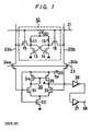
- Figure 1is a schematic diagram showing a construction of such a prior art sensing amplifier.
- a memory cell 10is provided, which is a component of a metal oxide semiconductor (MOS) memory matrix, not shown.
- the memory cell 10includes a flip-flop circuit formed of load resistors 11 and 12, and metal oxide semiconductor field effect transistors (MOSFET's) 13 and 14.
- This memory cell 10is of a static type memory which stores information each time the MOSFET's 13 and 14 are turned on or off.
- MOSFET's 15 and 16 connected to this word line 21are turned on, and the information stored in the memory cell 10 is transferred to Y addresses (bit lines) 22a and 22b.
- a selection signal for predetermined Y addresses (bit lines) 22a and 22bare supplied through a selection line 23 to MOSFET's 24a and 24b from a Y decoder, not shown. Then, the MOSFET's 24a and 24b are turned on, supplying the information of the predetermined memory cell 10 through the bit lines 22a and 22b to the sensing amplifier.
- a first stage amplifying circuit 30 of the sensing amplifieris formed as a current mirror type differential amplifying circuit.
- the first stage amplifying circuit 30comprises N-channel differential input MOSFET's 31 and 32 whose gates are respectively connected to the bit lines 22a and 22b.
- the sources of both the MOSFET's 31 and 32are connected together to a drain of a third N-channel MOSFET 33 that serves as a constant current source.
- the source of the MOSFET 33is grounded and the gate thereof is connected to a voltage source terminal TP and thereby the MOSFET 33 is turned on.
- the drains of both the N-channel MOSFET's 31 and 32are connected respectively to drains of a pair of P-channel MOSFET's 34 and 35, each of which is used as an active load.
- the gate and the drain of the P-channel MOSFET 34are directly coupled together to serve as a diode, while the gate of the other P-channel MOSFET 35 is connected to the gate of the MOSFET 34.
- the sources of both the P-channel MOSFET's 34 and 35are connected to the power source terminal TP.
- the current mirror circuitis constructed.
- differential amplifying circuit 30potentials or voltages having voltage levels corresponding to the on or off state of both the input differential MOSFET's 13 and 14 in the memory cell 10 and generated on both the bit lines 22a and 22b are supplied to the gates of both the input differential MOSFET's 31 and 32 as input signals thereof.
- a difference signal between these input signalsis amplified and from a connection point A between the MOSFET's 32 and 35, an unbalanced output signal of the differential amplifying circuit 30 is supplied to a driving stage, inverting amplifying circuit 36.
- the output signal from this inverting, amplifying circuit 36is supplied to an output stage, buffer amplifying circuit 37.
- the output signal from the output amplifying circuit 37has already reached a predetermined voltage level, and it is delivered through an output terminal 38 to a logic circuit, not shown.
- the output amplifying circuit 37has a large driving capacity.
- a transient current having a large amplitudeflows through the output amplifying circuit 37 to the voltage source and the ground, generating high frequency noises.
- the noisesare supplied through the voltage source and the ground to the differential amplifying circuit 30 in the same phase.
- the differential amplifying circuitamplifies a difference signal between two input signals and it does not amplify the input voltages having the same phase.
- the MOSFET 34 forming a part of the current mirror circuitis connected so as to operate as a diode and is low in impedance, while the other MOSFET 35 is high in impedance so that the loads to both the input differential FET's 31 and 32 are made asymmetric.
- DE-A-33 46 529discloses a sensing amplifier for use with a random access memory, said amplifier comprising:
- the loads in the first stage differential amplifying circuitare established by transistors receiving a supply voltage. Therefor, it is not possible to modify the load by a bias voltage as it is in principle possible with the arrangement of Fig. 1 as explained above.
- the amplifier of DE-A-33 46 529has the advantage that the first stage differential amplifying circuit is symmetrical due to the transistors as loads, thereby preventing the disadvantages as discussed in connection with the sensing amplifier according to Fig. 1.
- the sensing amplifier of the present inventioncomprises the following features:
- the first stage differential amplifying circuitDue to the symmetrical construction of the first stage differential amplifying circuit, noise components can be removed. Due to the special arrangement of the bias circuit and the first stage differential amplifying circuit, the latter circuit is still symmetrical when bias voltages are applied to it. This is described in detail in the description of Fig. 2.
- a first stage amplifying circuit 40is of a differential amplifying circuit type which includes symmetrical active loads.
- the bit lines 22a and 22bare respectively connected to gates of N-channel differential input MOSFET's 41 and 42 in the first differential amplifying circuit 40.
- the sources of both the MOSFET's 41 and 42are connected together to a drain of a third N-channel MOSFET 43 that serves as a constant current source.
- the source of the MOSFET 43is grounded.
- the drains of both the N-channel MOSFET's 41 and 42are connected respectively to drains of a pair of P-channel MOSFET's 44 and 45 which become symmetrical active loads.
- the sources of the MOSFET's 44 and 45are both connected to a power source terminal TP.
- a bias circuit 46supplies a bias voltage to the first stage amplifying circuit 40.
- the bias circuit 46comprises one P-channel MOSFET 47 and two N-channel MOSFET's 48 and 49 which are connected in series between the power source terminal TP and the ground.
- the source and the drain of the P-channel MOSFET 47are respectively connected to the power source terminal TP and the drain of the N-channel MOSFET 48, the source of the MOSFET 48 and the drain of the MOSFET 49 are connected together, and the source of the MOSFET 49 is grounded.
- the gate and the drain of the P-channel MOSFET 47are directly coupled to each other so as to operate as a diode and from a junction B at the connection between the MOSFET's 47 and 48, a bias voltage is commonly supplied to the gates of the pair of P-channel MOSFET's 44 and 45 in the differential amplifying circuit 40. Also, from this junction B, the common bias voltage is supplied to the gate of the MOSFET 49 of the bias circuit 46 and to the gate of the MOSFET 43 serving as the constant current source of the differential amplifying circuit 40.
- the gate of the MOSFET 48 in the bias circuit 46is connected to the gate of the MOSFET 42 in the differential amplifying circuit 40.
- the differential amplifying circuit 40generates balanced outputs at a junction C between the input differential MOSFET 41 and the active load, i.e., MOSFET 44, and a junction D between the input differential MOSFET 42 and the active load, i.e., MOSFET 45.
- a driving stage amplifying circuit 50is formed as a current mirror-type differential amplifying circuit similar to the foregoing first stage amplifying circuit 30 shown in Figure 1. Therefore, in the driving stage differential amplifying circuit 50 shown in Figure 2, like parts corresponding to those of the first stage amplifying circuit 30 are marked with reference numerals similar to those in Figure 1 in which reference numerals on the first order are not changed but reference numerals on the second order are replaced with "5". Thus, the circuit arrangement thereof will not be described in detail.
- the gate of the MOSFET 53 serving as the constant current sourceis supplied with the bias voltage from the MOSFET 54 whose gate and drain are coupled so as to operate as a diode in the current mirror circuit.
- the drain of the MOSFET 54is connected to the drain of the MOSFET 51 and a junction E therebetween is connected to the gate of the MOSFET 53.
- the differential input MOSFET's 51 and 52are supplied at their gates with the balanced outputs from the junctions C and D, respectively, of the first stage differential amplifying circuit 40. From the junction E between the drains of the MOSFET's 51 and 54, there is supplied a bias voltage to the gate of the MOSFET 55. Further, from a junction F between the MOSFET's 52 and 55, an unbalanced output of the differential amplifying circuit 50 is supplied to the output amplifying circuit 37. An output having a predetermined level from this output amplifying circuit 37 is delivered to the output terminal 38.
- the active loadsi.e., MOSFET's 44 and 45 in the differential amplifying circuit 40 and the MOSFET 47 whose gate and drain are coupled so as to operate as a diode in the bias circuit 46 are respectively formed to occupy the same dimension or area. For this reason, drain currents I44 and I45 of both the MOSFET's 44 and 45 become equal to a drain current I47 of the MOSFET 47. Further, since a drain current equal to those of the respective input differential MOSFET's 41 and 42 flows through the MOSFET 48 in the bias circuit 46, DC voltage drops across both the input differential MOSFET's 41 and 42 and across the bias MOSFET 48 become equal to one another.
- Both the junctions C and D of the first stage differential amplifying circuit 40are respectively connected to the gates of the differential input MOSFET's 51 and 52 in the driving stage differential amplifying circuit 50, so that the first stage differential amplifying circuit 40 is made sufficiently symmetrical (balanced) in the circuit arrangement from its input circuit to its output circuit.
- the noise components which are the same in phasecan be removed well within the first stage differential amplifying circuit 40 so that they can be prevented from being transmitted to the driving stage differential amplifying circuit 50.
- the driving stage amplifying circuit 50is formed of a differential amplifying circuit and the DC voltages having the same phase applied to the input differential MOSFET's 51 and 52 thereof can be varied over a wide range, when the input differential MOSFET's 51 and 52 are respectively connected to the pair of junctions (output terminals) C and D of the first stage differential amplifying circuit 40, it is not necessary to take a DC level difference therebetween into consideration.
- the first stage differential amplifying circuitis formed as a symmetrical (balanced) type and the driving stage circuit is formed as a differential amplifying circuit, it is possible to obtain a sensing amplifier which can sufficiently remove noise components which are the same in phase and which is free from the consideration of the DC level difference between the stages.
Landscapes
- Static Random-Access Memory (AREA)
- Amplifiers (AREA)
- Manipulation Of Pulses (AREA)
Description
- This invention relates generally to sensing amplifiers and, more particularly, is directed to a sensing amplifier for a random access memory (RAM) that is suitably used to amplify a signal read out from a memory.
- In the prior art, a sensing amplifier is used to amplify a signal having quite a low level read out from in internal storage or external storage (memory) of an electronic computer such that the level of such a signal read out reaches the voltage level to be processable by a logic circuit.
- An example of a prior art sensing amplifier will be described with reference to Figure 1. Figure 1 is a schematic diagram showing a construction of such a prior art sensing amplifier.
- Referring to Figure 1, a
memory cell 10 is provided, which is a component of a metal oxide semiconductor (MOS) memory matrix, not shown. Thememory cell 10 includes a flip-flop circuit formed ofload resistors memory cell 10 is of a static type memory which stores information each time the MOSFET's 13 and 14 are turned on or off. When thememory cell 10 is put in the reading mode, if an X address (word line) 21 is selected by an X decoder, not shown, MOSFET's 15 and 16 connected to thisword line 21 are turned on, and the information stored in thememory cell 10 is transferred to Y addresses (bit lines) 22a and 22b. In this case, since the memory cells on thesame word line 21 are all activated, a selection signal for predetermined Y addresses (bit lines) 22a and 22b are supplied through aselection line 23 to MOSFET's 24a and 24b from a Y decoder, not shown. Then, the MOSFET's 24a and 24b are turned on, supplying the information of thepredetermined memory cell 10 through thebit lines - A first
stage amplifying circuit 30 of the sensing amplifier is formed as a current mirror type differential amplifying circuit. To be more concrete, the firststage amplifying circuit 30 comprises N-channel differential input MOSFET's 31 and 32 whose gates are respectively connected to thebit lines channel MOSFET 33 that serves as a constant current source. The source of theMOSFET 33 is grounded and the gate thereof is connected to a voltage source terminal TP and thereby theMOSFET 33 is turned on. The drains of both the N-channel MOSFET's 31 and 32 are connected respectively to drains of a pair of P-channel MOSFET's 34 and 35, each of which is used as an active load. The gate and the drain of the P-channel MOSFET 34 are directly coupled together to serve as a diode, while the gate of the other P-channel MOSFET 35 is connected to the gate of theMOSFET 34. Then, the sources of both the P-channel MOSFET's 34 and 35 are connected to the power source terminal TP. Thus, the current mirror circuit is constructed. - In the above-mentioned differential amplifying
circuit 30, potentials or voltages having voltage levels corresponding to the on or off state of both the input differential MOSFET's 13 and 14 in thememory cell 10 and generated on both thebit lines circuit 30 is supplied to a driving stage, inverting amplifyingcircuit 36. The output signal from this inverting, amplifyingcircuit 36 is supplied to an output stage,buffer amplifying circuit 37. The output signal from theoutput amplifying circuit 37 has already reached a predetermined voltage level, and it is delivered through anoutput terminal 38 to a logic circuit, not shown. - A sensing amplifier used for a memory capable of operating at high speed and producing multiple-outputs, the
output amplifying circuit 37 has a large driving capacity. Thus, when a load having a large capacity is connected to theoutput terminal 38, a transient current having a large amplitude flows through theoutput amplifying circuit 37 to the voltage source and the ground, generating high frequency noises. The noises are supplied through the voltage source and the ground to the differential amplifyingcircuit 30 in the same phase. - Of course, as is well known in the art, the differential amplifying circuit amplifies a difference signal between two input signals and it does not amplify the input voltages having the same phase. However, in the conventional current mirror type differential amplifying
circuit 30 shown in Figure 1, theMOSFET 34 forming a part of the current mirror circuit is connected so as to operate as a diode and is low in impedance, while theother MOSFET 35 is high in impedance so that the loads to both the input differential FET's 31 and 32 are made asymmetric. As a result, when the high frequency response characteristic of the constantcurrent source FET 33 is not sufficient, the above-mentioned noise components having the same phase can not be cancelled out within the differential amplifyingcircuit 30 and appear at the junction A between the MOSFET's 32 and 35, preventing a signal from being read out correctly from the memory. - DE-A-33 46 529 discloses a sensing amplifier for use with a random access memory, said amplifier comprising:
- a symmetrical first stage differential amplifying circuit comprising a pair of amplifying transistors receiving read-out signals at their gates and a pair of MOSFET's as loads, and
- a driving stage differential amplifying circuit.
- The loads in the first stage differential amplifying circuit are established by transistors receiving a supply voltage. Therefor, it is not possible to modify the load by a bias voltage as it is in principle possible with the arrangement of Fig. 1 as explained above. However, the amplifier of DE-A-33 46 529 has the advantage that the first stage differential amplifying circuit is symmetrical due to the transistors as loads, thereby preventing the disadvantages as discussed in connection with the sensing amplifier according to Fig. 1.
- It is the object of the present invention to provide a sensing amplifier for use with a random access memory, said amplifier having a symmetrical first stage to be able to remove noise components, and being arranged to have applied a bias voltage for adjustment purposes.
- The sensing amplifier of the present invention comprises the following features:
- a symmetrical first stage differential amplifying circuit comprising a pair of amplifying transistors receiving read-out signals at their gates, and comprising first and second MOSFET's as loads,
- a bias circuit for biasing said load-MOSFETs and comprising a third MOSFET having its gate and drain coupled to operate as a diode, and
- a driving stage differential amplifying circuit,
- whereby said three MOSFETs are all of the same type, are all connected to a power source terminal with their drains, all receive the bias voltage at their gate, and all occupy the same dimension or area.
- The invention is set forth in independent claim 1.
- Due to the symmetrical construction of the first stage differential amplifying circuit, noise components can be removed. Due to the special arrangement of the bias circuit and the first stage differential amplifying circuit, the latter circuit is still symmetrical when bias voltages are applied to it. This is described in detail in the description of Fig. 2.
- These and other objects, features and advantages of the present invention will become apparent from the following detailed description of the preferred embodiment taken in conjunction with the accompanying drawing.
- Figure 1 is a schematic diagram showing a construction of a prior art sensing amplifier; and
- Figure 2 is a schematic diagram showing an embodiment of a sensing amplifier for a random access memory according to the present invention.
- A first
stage amplifying circuit 40 is of a differential amplifying circuit type which includes symmetrical active loads. Specifically, thebit lines circuit 40. The sources of both the MOSFET's 41 and 42 are connected together to a drain of a third N-channel MOSFET 43 that serves as a constant current source. The source of the MOSFET 43 is grounded. The drains of both the N-channel MOSFET's 41 and 42 are connected respectively to drains of a pair of P-channel MOSFET's 44 and 45 which become symmetrical active loads. The sources of the MOSFET's 44 and 45 are both connected to a power source terminal TP. - A
bias circuit 46 supplies a bias voltage to the firststage amplifying circuit 40. Thebias circuit 46 comprises one P-channel MOSFET 47 and two N-channel MOSFET's 48 and 49 which are connected in series between the power source terminal TP and the ground. In other words, in thebias circuit 46, the source and the drain of the P-channel MOSFET 47 are respectively connected to the power source terminal TP and the drain of the N-channel MOSFET 48, the source of theMOSFET 48 and the drain of theMOSFET 49 are connected together, and the source of theMOSFET 49 is grounded. - The gate and the drain of the P-
channel MOSFET 47 are directly coupled to each other so as to operate as a diode and from a junction B at the connection between the MOSFET's 47 and 48, a bias voltage is commonly supplied to the gates of the pair of P-channel MOSFET's 44 and 45 in the differential amplifyingcircuit 40. Also, from this junction B, the common bias voltage is supplied to the gate of theMOSFET 49 of thebias circuit 46 and to the gate of the MOSFET 43 serving as the constant current source of the differential amplifyingcircuit 40. The gate of theMOSFET 48 in thebias circuit 46 is connected to the gate of the MOSFET 42 in the differential amplifyingcircuit 40. The differential amplifyingcircuit 40 generates balanced outputs at a junction C between the inputdifferential MOSFET 41 and the active load, i.e., MOSFET 44, and a junction D between the input differential MOSFET 42 and the active load, i.e.,MOSFET 45. - A driving
stage amplifying circuit 50 is formed as a current mirror-type differential amplifying circuit similar to the foregoing firststage amplifying circuit 30 shown in Figure 1. Therefore, in the driving stage differential amplifyingcircuit 50 shown in Figure 2, like parts corresponding to those of the firststage amplifying circuit 30 are marked with reference numerals similar to those in Figure 1 in which reference numerals on the first order are not changed but reference numerals on the second order are replaced with "5". Thus, the circuit arrangement thereof will not be described in detail. - In this differential amplifying
circuit 50, the gate of theMOSFET 53 serving as the constant current source is supplied with the bias voltage from theMOSFET 54 whose gate and drain are coupled so as to operate as a diode in the current mirror circuit. The drain of theMOSFET 54 is connected to the drain of theMOSFET 51 and a junction E therebetween is connected to the gate of theMOSFET 53. - In the driving stage
differential amplifying circuit 50, the differential input MOSFET's 51 and 52 are supplied at their gates with the balanced outputs from the junctions C and D, respectively, of the first stagedifferential amplifying circuit 40. From the junction E between the drains of the MOSFET's 51 and 54, there is supplied a bias voltage to the gate of theMOSFET 55. Further, from a junction F between the MOSFET's 52 and 55, an unbalanced output of thedifferential amplifying circuit 50 is supplied to theoutput amplifying circuit 37. An output having a predetermined level from thisoutput amplifying circuit 37 is delivered to theoutput terminal 38. - The operation of the sensing amplifier according to the above embodiment will now be described.
- The active loads, i.e., MOSFET's 44 and 45 in the
differential amplifying circuit 40 and theMOSFET 47 whose gate and drain are coupled so as to operate as a diode in thebias circuit 46 are respectively formed to occupy the same dimension or area. For this reason, drain currents I44 and I45 of both the MOSFET's 44 and 45 become equal to a drain current I47 of theMOSFET 47. Further, since a drain current equal to those of the respective input differential MOSFET's 41 and 42 flows through theMOSFET 48 in thebias circuit 46, DC voltage drops across both the input differential MOSFET's 41 and 42 and across thebias MOSFET 48 become equal to one another. Accordingly, also DC voltage drops across the active loads, i.e., the MOSFET's 44 and 45 in the first stagedifferential amplifying circuit 40 become equal to each other so that both the active loads, i.e., the MOSFET's 44 and 45 become sufficiently symmetrical to each other. - Both the junctions C and D of the first stage
differential amplifying circuit 40 are respectively connected to the gates of the differential input MOSFET's 51 and 52 in the driving stagedifferential amplifying circuit 50, so that the first stagedifferential amplifying circuit 40 is made sufficiently symmetrical (balanced) in the circuit arrangement from its input circuit to its output circuit. - Therefore, according to this embodiment, even when the noise components which are the same in phase enter through the power source terminal and the ground, as mentioned before, the noise components having the same phase can be removed well within the first stage
differential amplifying circuit 40 so that they can be prevented from being transmitted to the driving stagedifferential amplifying circuit 50. - Moreover, since the driving
stage amplifying circuit 50 is formed of a differential amplifying circuit and the DC voltages having the same phase applied to the input differential MOSFET's 51 and 52 thereof can be varied over a wide range, when the input differential MOSFET's 51 and 52 are respectively connected to the pair of junctions (output terminals) C and D of the first stagedifferential amplifying circuit 40, it is not necessary to take a DC level difference therebetween into consideration. - According to the present invention as described above in detail, since the first stage differential amplifying circuit is formed as a symmetrical (balanced) type and the driving stage circuit is formed as a differential amplifying circuit, it is possible to obtain a sensing amplifier which can sufficiently remove noise components which are the same in phase and which is free from the consideration of the DC level difference between the stages.
Claims (3)
- A sensing amplifier for use with a random access memory, said amplifier comprising:- a symmetrical first stage differential amplifying circuit (40), comprising a pair of amplifying transistors (41, 42) receiving read-out signals at their gates, and first and second MOSFETs (44, 45) as loads, and- a driving stage differential amplifying circuit (50).characterized in that- a bias circuit (46) is provided for biasing said load-MOSFETs, said bias circuit comprising a third MOSFET (47) having its gate and drain coupled to operate as a diode,- whereby said three MOSFETs (44, 45, 47) are all of the same type, are all connected to a power source terminal (TP) with their drains, all receive the bias voltage at their gates, and all occupy the same dimension or area.
- A sensing amplifier according to claim 1,characterized in that said first stage differential amplifying circuit (40) comprises a constant current source having a transistor (43) whose drain is connected to the source of said amplifying transistors (41, 42), whose source is grounded and whose gate is supplied with the bias voltage.
- A sensing amplifier according to one of the claims 1 or 2,characterized in that said bias circuit (46) comprises a fourth MOSFET (48) having its gate connected to one of the read-out memory signals, its drain connected to the drain of the third MOSFET (47), and its source connected to the drain of a fifth MOSFET (49), said fifth MOSFET having its gate connected to the drains of said third and fourth MOSFETs and its source connected to ground.
Applications Claiming Priority (2)
| Application Number | Priority Date | Filing Date | Title |
|---|---|---|---|
| JP60065876AJPS61224192A (en) | 1985-03-29 | 1985-03-29 | Reading amplifier |
| JP65876/85 | 1985-03-29 |
Publications (3)
| Publication Number | Publication Date |
|---|---|
| EP0196110A2 EP0196110A2 (en) | 1986-10-01 |
| EP0196110A3 EP0196110A3 (en) | 1988-08-03 |
| EP0196110B1true EP0196110B1 (en) | 1992-01-02 |
Family
ID=13299616
Family Applications (1)
| Application Number | Title | Priority Date | Filing Date |
|---|---|---|---|
| EP86104290AExpiredEP0196110B1 (en) | 1985-03-29 | 1986-03-27 | Sensing amplifier for random access memory |
Country Status (4)
| Country | Link |
|---|---|
| US (1) | US4724344A (en) |
| EP (1) | EP0196110B1 (en) |
| JP (1) | JPS61224192A (en) |
| DE (1) | DE3683177D1 (en) |
Families Citing this family (19)
| Publication number | Priority date | Publication date | Assignee | Title |
|---|---|---|---|---|
| US4788510A (en)* | 1987-05-29 | 1988-11-29 | American Telephone And Telegraph Company, At&T Bell Laboratories | Differential input stage for differential line receivers and operational amplifiers |
| US4949306A (en)* | 1987-06-19 | 1990-08-14 | Hitachi, Ltd. | Sense circuit and semiconductor memory having a current-voltage converter circuit |
| US4954992A (en)* | 1987-12-24 | 1990-09-04 | Mitsubishi Denki Kabushiki Kaisha | Random access memory having separate read out and write in bus lines for reduced access time and operating method therefor |
| US5053652A (en)* | 1988-01-28 | 1991-10-01 | Hitachi, Ltd. | High speed sensor system using a level shift circuit |
| FR2628547B1 (en)* | 1988-03-09 | 1990-12-28 | Sgs Thomson Microelectronics | STABILIZED GENERATOR FOR PROVIDING MOS TRANSISTOR THRESHOLD |
| US4918341A (en)* | 1988-09-23 | 1990-04-17 | Actel Corporaton | High speed static single-ended sense amplifier |
| US5179538A (en)* | 1989-06-30 | 1993-01-12 | The Boeing Company | Memory system including CMOS memory cells and bipolar sensing circuit |
| US5099156A (en)* | 1990-10-02 | 1992-03-24 | California Institute Of Technology | Subthreshold MOS circuits for correlating analog input voltages |
| US5089726A (en)* | 1990-11-29 | 1992-02-18 | International Business Machines Corporation | Fast cycle time clocked amplifier |
| KR920013458A (en)* | 1990-12-12 | 1992-07-29 | 김광호 | Differential Detection Amplifier |
| KR940003836B1 (en)* | 1991-03-06 | 1994-05-03 | 현대전자산업 주식회사 | Data sensing circuit |
| US5172016A (en)* | 1991-06-28 | 1992-12-15 | Digital Equipment Corporation | Five-volt tolerant differential receiver |
| JPH0636570A (en)* | 1992-07-16 | 1994-02-10 | Mitsubishi Electric Corp | Sense amplifier circuit for semiconductor memory |
| DE4227282C1 (en)* | 1992-08-18 | 1993-11-25 | Siemens Ag | Digital power switch |
| US5568438A (en)* | 1995-07-18 | 1996-10-22 | Analog Devices, Inc. | Sense amplifier with offset autonulling |
| KR100196510B1 (en)* | 1995-12-28 | 1999-06-15 | 김영환 | Sense amplifier |
| GB9906973D0 (en)* | 1999-03-25 | 1999-05-19 | Sgs Thomson Microelectronics | Sense amplifier circuit |
| JP2004274207A (en)* | 2003-03-06 | 2004-09-30 | Renesas Technology Corp | Bias voltage generator circuit and differential amplifier |
| US9911501B2 (en)* | 2016-05-24 | 2018-03-06 | Silicon Storage Technology, Inc. | Sensing amplifier comprising a built-in sensing offset for flash memory devices |
Family Cites Families (8)
| Publication number | Priority date | Publication date | Assignee | Title |
|---|---|---|---|---|
| JPS5824874B2 (en)* | 1979-02-07 | 1983-05-24 | 富士通株式会社 | sense circuit |
| US4223394A (en)* | 1979-02-13 | 1980-09-16 | Intel Corporation | Sensing amplifier for floating gate memory devices |
| JPS6032912B2 (en)* | 1979-09-13 | 1985-07-31 | 株式会社東芝 | CMOS sense amplifier circuit |
| JPS57198594A (en)* | 1981-06-01 | 1982-12-06 | Hitachi Ltd | Semiconductor storage device |
| US4471244A (en)* | 1981-07-22 | 1984-09-11 | Data General Corporation | Sense amplifier |
| JPS58168310A (en)* | 1982-03-30 | 1983-10-04 | Fujitsu Ltd | Differential amplifying circuit |
| US4604533A (en)* | 1982-12-28 | 1986-08-05 | Tokyo Shibaura Denki Kabushiki Kaisha | Sense amplifier |
| US4598215A (en)* | 1983-11-03 | 1986-07-01 | Motorola, Inc. | Wide common mode range analog CMOS voltage comparator |
- 1985
- 1985-03-29JPJP60065876Apatent/JPS61224192A/enactivePending
- 1986
- 1986-03-27EPEP86104290Apatent/EP0196110B1/ennot_activeExpired
- 1986-03-27DEDE8686104290Tpatent/DE3683177D1/ennot_activeExpired - Lifetime
- 1986-03-28USUS06/845,649patent/US4724344A/ennot_activeExpired - Fee Related
Also Published As
| Publication number | Publication date |
|---|---|
| DE3683177D1 (en) | 1992-02-13 |
| JPS61224192A (en) | 1986-10-04 |
| EP0196110A2 (en) | 1986-10-01 |
| EP0196110A3 (en) | 1988-08-03 |
| US4724344A (en) | 1988-02-09 |
Similar Documents
| Publication | Publication Date | Title |
|---|---|---|
| EP0196110B1 (en) | Sensing amplifier for random access memory | |
| US4697112A (en) | Current-mirror type sense amplifier | |
| US4728900A (en) | Balanced differential amplifier | |
| RU2119243C1 (en) | Differential reading amplifier | |
| US6703871B2 (en) | Amplifier for use in semiconductor integrated circuits | |
| US4670675A (en) | High gain sense amplifier for small current differential | |
| US5537066A (en) | Flip-flop type amplifier circuit | |
| US4937479A (en) | Data latch circuit with improved data write control function | |
| US5699305A (en) | Amplifier and semiconductor memory device having the same | |
| US4860257A (en) | Level shifter for an input/output bus in a CMOS dynamic ram | |
| JP2756797B2 (en) | FET sense amplifier | |
| US4658160A (en) | Common gate MOS differential sense amplifier | |
| US5412607A (en) | Semiconductor memory device | |
| EP0365730A1 (en) | Double stage bipolar sense amplifier for BICMOS SRAMS with a common base amplifier in the final stage | |
| US6243314B1 (en) | Apparatus for sensing a current direction of an input signal and amplifying the sensed input signal in semiconductor memory device | |
| JPS6196587A (en) | sense amplifier circuit | |
| JP2680939B2 (en) | Semiconductor memory device | |
| US6128236A (en) | Current sensing differential amplifier with high rejection of power supply variations and method for an integrated circuit memory device | |
| US5293515A (en) | Amplifier circuit having two inverters | |
| JP2514988B2 (en) | Sense amplifier circuit | |
| JPH0743938B2 (en) | Differential amplifier | |
| EP0417973A2 (en) | Amplifier circuit having two inverters | |
| JP3154502B2 (en) | Signal amplifier circuit and semiconductor memory device using the same | |
| JPH0734312B2 (en) | Sense circuit | |
| JPH0246595A (en) | sense amplifier |
Legal Events
| Date | Code | Title | Description |
|---|---|---|---|
| PUAI | Public reference made under article 153(3) epc to a published international application that has entered the european phase | Free format text:ORIGINAL CODE: 0009012 | |
| AK | Designated contracting states | Kind code of ref document:A2 Designated state(s):DE FR GB NL | |
| PUAL | Search report despatched | Free format text:ORIGINAL CODE: 0009013 | |
| AK | Designated contracting states | Kind code of ref document:A3 Designated state(s):DE FR GB NL | |
| 17P | Request for examination filed | Effective date:19890120 | |
| 17Q | First examination report despatched | Effective date:19900720 | |
| GRAA | (expected) grant | Free format text:ORIGINAL CODE: 0009210 | |
| AK | Designated contracting states | Kind code of ref document:B1 Designated state(s):DE FR GB NL | |
| REF | Corresponds to: | Ref document number:3683177 Country of ref document:DE Date of ref document:19920213 | |
| ET | Fr: translation filed | ||
| PLBE | No opposition filed within time limit | Free format text:ORIGINAL CODE: 0009261 | |
| STAA | Information on the status of an ep patent application or granted ep patent | Free format text:STATUS: NO OPPOSITION FILED WITHIN TIME LIMIT | |
| 26N | No opposition filed | ||
| PGFP | Annual fee paid to national office [announced via postgrant information from national office to epo] | Ref country code:FR Payment date:19970313 Year of fee payment:12 | |
| PGFP | Annual fee paid to national office [announced via postgrant information from national office to epo] | Ref country code:GB Payment date:19970318 Year of fee payment:12 | |
| PGFP | Annual fee paid to national office [announced via postgrant information from national office to epo] | Ref country code:NL Payment date:19970327 Year of fee payment:12 | |
| PGFP | Annual fee paid to national office [announced via postgrant information from national office to epo] | Ref country code:DE Payment date:19970404 Year of fee payment:12 | |
| PG25 | Lapsed in a contracting state [announced via postgrant information from national office to epo] | Ref country code:GB Free format text:LAPSE BECAUSE OF NON-PAYMENT OF DUE FEES Effective date:19980327 | |
| PG25 | Lapsed in a contracting state [announced via postgrant information from national office to epo] | Ref country code:FR Free format text:THE PATENT HAS BEEN ANNULLED BY A DECISION OF A NATIONAL AUTHORITY Effective date:19980331 | |
| PG25 | Lapsed in a contracting state [announced via postgrant information from national office to epo] | Ref country code:NL Free format text:LAPSE BECAUSE OF NON-PAYMENT OF DUE FEES Effective date:19981001 | |
| GBPC | Gb: european patent ceased through non-payment of renewal fee | Effective date:19980327 | |
| NLV4 | Nl: lapsed or anulled due to non-payment of the annual fee | Effective date:19981001 | |
| PG25 | Lapsed in a contracting state [announced via postgrant information from national office to epo] | Ref country code:DE Free format text:LAPSE BECAUSE OF NON-PAYMENT OF DUE FEES Effective date:19981201 | |
| REG | Reference to a national code | Ref country code:FR Ref legal event code:ST |