EP0194323B1 - Scanning tunneling microscope - Google Patents
Scanning tunneling microscopeDownload PDFInfo
- Publication number
- EP0194323B1 EP0194323B1EP85102554AEP85102554AEP0194323B1EP 0194323 B1EP0194323 B1EP 0194323B1EP 85102554 AEP85102554 AEP 85102554AEP 85102554 AEP85102554 AEP 85102554AEP 0194323 B1EP0194323 B1EP 0194323B1
- Authority
- EP
- European Patent Office
- Prior art keywords
- tip
- chip
- tongue
- scanning tunneling
- tunneling microscope
- Prior art date
- Legal status (The legal status is an assumption and is not a legal conclusion. Google has not performed a legal analysis and makes no representation as to the accuracy of the status listed.)
- Expired
Links
- 230000005641tunnelingEffects0.000titleclaimsdescription26
- 229910052710siliconInorganic materials0.000claimsdescription18
- 239000010703siliconSubstances0.000claimsdescription18
- 239000004065semiconductorSubstances0.000claimsdescription14
- 238000005530etchingMethods0.000claimsdescription13
- 229910052751metalInorganic materials0.000claimsdescription7
- 239000002184metalSubstances0.000claimsdescription7
- 238000005452bendingMethods0.000claimsdescription6
- 238000004519manufacturing processMethods0.000claimsdescription6
- 239000000463materialSubstances0.000claimsdescription6
- 238000000034methodMethods0.000claimsdescription6
- 239000011159matrix materialSubstances0.000claimsdescription5
- 238000009877renderingMethods0.000claimsdescription5
- 239000004020conductorSubstances0.000claimsdescription4
- 239000011248coating agentSubstances0.000claimsdescription3
- 238000000576coating methodMethods0.000claimsdescription3
- 238000000151depositionMethods0.000claimsdescription3
- 210000002105tongueAnatomy0.000claims9
- 238000011835investigationMethods0.000claims1
- XUIMIQQOPSSXEZ-UHFFFAOYSA-NSiliconChemical compound[Si]XUIMIQQOPSSXEZ-UHFFFAOYSA-N0.000description16
- 235000012431wafersNutrition0.000description9
- VYPSYNLAJGMNEJ-UHFFFAOYSA-NSilicium dioxideChemical compoundO=[Si]=OVYPSYNLAJGMNEJ-UHFFFAOYSA-N0.000description5
- 238000013461designMethods0.000description5
- 229910021421monocrystalline siliconInorganic materials0.000description5
- 229910052681coesiteInorganic materials0.000description4
- 229910052906cristobaliteInorganic materials0.000description4
- 239000013078crystalSubstances0.000description4
- 229910052682stishoviteInorganic materials0.000description4
- 229910052905tridymiteInorganic materials0.000description4
- 230000001276controlling effectEffects0.000description3
- 230000033001locomotionEffects0.000description3
- 230000005693optoelectronicsEffects0.000description3
- 238000012545processingMethods0.000description3
- 230000008901benefitEffects0.000description2
- 230000006835compressionEffects0.000description2
- 238000007906compressionMethods0.000description2
- 229910003460diamondInorganic materials0.000description2
- 239000010432diamondSubstances0.000description2
- 230000005684electric fieldEffects0.000description2
- 150000002739metalsChemical class0.000description2
- 238000005459micromachiningMethods0.000description2
- 238000012876topographyMethods0.000description2
- 229910000838Al alloyInorganic materials0.000description1
- OKTJSMMVPCPJKN-UHFFFAOYSA-NCarbonChemical compound[C]OKTJSMMVPCPJKN-UHFFFAOYSA-N0.000description1
- 229910000676Si alloyInorganic materials0.000description1
- 229910000831SteelInorganic materials0.000description1
- 230000009471actionEffects0.000description1
- 230000004075alterationEffects0.000description1
- 229910052799carbonInorganic materials0.000description1
- 230000008859changeEffects0.000description1
- 238000010276constructionMethods0.000description1
- 238000001816coolingMethods0.000description1
- 230000002596correlated effectEffects0.000description1
- 230000008021depositionEffects0.000description1
- 238000009792diffusion processMethods0.000description1
- 238000006073displacement reactionMethods0.000description1
- 230000000694effectsEffects0.000description1
- 239000002305electric materialSubstances0.000description1
- 238000009713electroplatingMethods0.000description1
- 230000005496eutecticsEffects0.000description1
- 230000005669field effectEffects0.000description1
- 238000002171field ion microscopyMethods0.000description1
- 238000009413insulationMethods0.000description1
- 230000010354integrationEffects0.000description1
- 239000007788liquidSubstances0.000description1
- 238000001459lithographyMethods0.000description1
- 230000000873masking effectEffects0.000description1
- 238000005259measurementMethods0.000description1
- 230000007246mechanismEffects0.000description1
- 239000000155meltSubstances0.000description1
- 239000012528membraneSubstances0.000description1
- 238000004377microelectronicMethods0.000description1
- 230000005012migrationEffects0.000description1
- 238000013508migrationMethods0.000description1
- 230000000737periodic effectEffects0.000description1
- 230000008569processEffects0.000description1
- 230000004044responseEffects0.000description1
- 230000000284resting effectEffects0.000description1
- 238000012552reviewMethods0.000description1
- 238000000926separation methodMethods0.000description1
- 230000008054signal transmissionEffects0.000description1
- 239000000377silicon dioxideSubstances0.000description1
- 238000004544sputter depositionMethods0.000description1
- 239000010959steelSubstances0.000description1
- 230000003746surface roughnessEffects0.000description1
- 238000012546transferMethods0.000description1
Images


Classifications
- H—ELECTRICITY
- H01—ELECTRIC ELEMENTS
- H01J—ELECTRIC DISCHARGE TUBES OR DISCHARGE LAMPS
- H01J37/00—Discharge tubes with provision for introducing objects or material to be exposed to the discharge, e.g. for the purpose of examination or processing thereof
- H01J37/02—Details
- H01J37/20—Means for supporting or positioning the object or the material; Means for adjusting diaphragms or lenses associated with the support
- G—PHYSICS
- G01—MEASURING; TESTING
- G01Q—SCANNING-PROBE TECHNIQUES OR APPARATUS; APPLICATIONS OF SCANNING-PROBE TECHNIQUES, e.g. SCANNING PROBE MICROSCOPY [SPM]
- G01Q10/00—Scanning or positioning arrangements, i.e. arrangements for actively controlling the movement or position of the probe
- G01Q10/04—Fine scanning or positioning
- G—PHYSICS
- G01—MEASURING; TESTING
- G01Q—SCANNING-PROBE TECHNIQUES OR APPARATUS; APPLICATIONS OF SCANNING-PROBE TECHNIQUES, e.g. SCANNING PROBE MICROSCOPY [SPM]
- G01Q60/00—Particular types of SPM [Scanning Probe Microscopy] or microscopes; Essential components thereof
- G01Q60/10—STM [Scanning Tunnelling Microscopy] or apparatus therefor, e.g. STM probes
- G01Q60/16—Probes, their manufacture, or their related instrumentation, e.g. holders
- G—PHYSICS
- G01—MEASURING; TESTING
- G01Q—SCANNING-PROBE TECHNIQUES OR APPARATUS; APPLICATIONS OF SCANNING-PROBE TECHNIQUES, e.g. SCANNING PROBE MICROSCOPY [SPM]
- G01Q70/00—General aspects of SPM probes, their manufacture or their related instrumentation, insofar as they are not specially adapted to a single SPM technique covered by group G01Q60/00
- G01Q70/02—Probe holders
- Y—GENERAL TAGGING OF NEW TECHNOLOGICAL DEVELOPMENTS; GENERAL TAGGING OF CROSS-SECTIONAL TECHNOLOGIES SPANNING OVER SEVERAL SECTIONS OF THE IPC; TECHNICAL SUBJECTS COVERED BY FORMER USPC CROSS-REFERENCE ART COLLECTIONS [XRACs] AND DIGESTS
- Y10—TECHNICAL SUBJECTS COVERED BY FORMER USPC
- Y10S—TECHNICAL SUBJECTS COVERED BY FORMER USPC CROSS-REFERENCE ART COLLECTIONS [XRACs] AND DIGESTS
- Y10S977/00—Nanotechnology
- Y10S977/84—Manufacture, treatment, or detection of nanostructure
- Y10S977/849—Manufacture, treatment, or detection of nanostructure with scanning probe
- Y10S977/86—Scanning probe structure
- Y10S977/861—Scanning tunneling probe
- Y—GENERAL TAGGING OF NEW TECHNOLOGICAL DEVELOPMENTS; GENERAL TAGGING OF CROSS-SECTIONAL TECHNOLOGIES SPANNING OVER SEVERAL SECTIONS OF THE IPC; TECHNICAL SUBJECTS COVERED BY FORMER USPC CROSS-REFERENCE ART COLLECTIONS [XRACs] AND DIGESTS
- Y10—TECHNICAL SUBJECTS COVERED BY FORMER USPC
- Y10S—TECHNICAL SUBJECTS COVERED BY FORMER USPC CROSS-REFERENCE ART COLLECTIONS [XRACs] AND DIGESTS
- Y10S977/00—Nanotechnology
- Y10S977/84—Manufacture, treatment, or detection of nanostructure
- Y10S977/849—Manufacture, treatment, or detection of nanostructure with scanning probe
- Y10S977/86—Scanning probe structure
- Y10S977/872—Positioner
Definitions
- This inventionrelates to a scanning tunneling microscope of the type where a sharply pointed tip is maintained at a constant distance from a specimen to be investigated, and wherein the variations of the tunnel current occurring as the tip is raster-scanned across the surface of specimen are employed to adjust said distance and to control a plotter or other recording device for generating an image of the specimen's topography.
- Scanning tunneling microscopes of this sortare well known in the art, e.g. from US ⁇ A ⁇ 4,343,993.
- Such scanning tunneling microscopescomprise a fine, electrically conducting tip, means for positioning a conductive specimen surface sufficiently close to said conductive tip so that a tunnel current flows, means for scanning said tip across the specimen's surfaces, means for automatically controlling the separation distance between said tip and the specimen surface while the tip is scanned across the surface in response to the measured tunnel effect, and means for graphically displaying the spatial coordinates of said scanning tip to produce a topological map of said surface.
- the distance between tip and specimen for a tunnel current to flowmust be of the order of 1 nanometer. Of course, at such small distances, the surface roughness at the specimen will cause frequent variations which have to be adjusted.
- the adjustment currentis used to control a graphics display or recorder to which the coordinates of the current scanning position are also supplied.
- the STM and all of its parts and aggregatesare designed as rather bulky devices, i.e. they have large dimensions (several centimeters) and, hence, both a relatively large mass and relatively low stiffness, (for example, a low bending stiffness proportional to the third power of the length) which results in a low resonance frequency. Since the vibrations occurring in any environment have a low frequency, it is desirable for vibration-sensitive apparatus to have a high resonance frequency. The best way of increasing the resonance frequency of a given design is to reduce its dimensions.
- an object of the present inventionto propose a scanning tunneling microscope which is of small design and very stiff construction and which does not show the disadvantages of the prior art scanning tunneling microscopes, thus permitting even higher resolution.
- the STM of the present inventionis easy and cheap to manufacture and operates at low voltages. It really opens an avenue to mass- production.
- the solution offered hereinlies in the design of the STM in the so-called silicon micromachining technique, i.e. the essential parts of the STM are implemented on a tiny silicon ship using micromechanical techniques which are per se known in the art.
- the silicon employed in the electronics industrytakes the form of single crystals which are grown from a melt and sliced into disk-shaped wafers from 0,2 to 0,5 mm thick.
- the homogeneous crystal structure of the materialgives it the electrical properties needed in microelectronic circuits.
- silicon in this formalso has desirable mechanical properties.
- Siliconhas its position in the periodic system directly below carbon and forms the same type of crystal as diamond.
- Single-crystal siliconis brittle and can be cleaved like diamond, but it is harder than most metals; it is extremely resistant to mechanical stress, it has a higher elastic limit in both, tension and compression than steel.
- single-crystal siliconremains strong under repeated cycles of tension and compression, whereas polycrystalline metals tend to weaken and break because stresses accumulate at the intercrystal boundaries.
- the scanning tunneling microscope of the present inventioncomprising at least one electron-emitting tip maintained at an essentially constant distance shorter than about 2 nm from the surface of a specimen to be investigated, an xy-drive for scanning said tip in a matrix fashion across said surface, and comprising means for controlling and displaying and/or recording the variations of the tunnel current and/ or the current required to maintain said distance essentially constant, thereby generating an image of the specimen's surface, is characterized in that said xy-drive consists of a semiconductor chip having a center portion connected by an intermediate portion and by two pairs of strips acting as leaf springs, to the main body of said chip, that said electron-emitting tip sits on a tongue forming an integral part of said center portion and being capable of being moved in a z-direction normal to the plane of said chip.
- the inventionfurther relates to a method for manufacturing a scanning tunneling microscope of the type described above, the method being characterized by the steps of preparing a ⁇ 110> oriented semiconductor chip, etching a four-sided portion at the center of said chip, which is linked by an intermediate portion and by two pairs of strips acting as leaf springs, to the main body of said chip, the slots between said strips and said center portion and said intermediate portion respectively being made parallel to the [111] and [1-11] directions of the semiconductor material of said chip, rendering selected parts of the vertical walls of said chip, said portions and said strips electrically conductive by doping said parts prior to etching and/or by depositing a metal layer thereon, underetching the area of said center portion of said chip supposed to carry said tip by using boron-doped layers, thus forming at least one tongue, growing a semiconductor platelet on said tongue, underetching said platelet to form said tip, and rendering said tip conductive by doping and/or coating with a film of conductive material.
- FIG. 1shows an embodiment of the scanning mechanism and distance control.
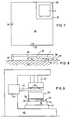
- An essentially square portion 1is linked by a first pair of strips 2 and 3 to an L-shaped portion 4, and the latter in turn is linked by a second pair of strips 5 and 6 to the body of a chip 7 which appears as if surrounding the combination of said square and L-shaped portions 1 and 4.
- the entire assembly comprising elements 1 through 7is one piece, the slots between the elements having been created by etching.
- a first horseshoeshaped slot 8 and a second, smaller and oppositely oriented, rectangular slot 10are etched through the entire thickness of chip 7 (which may be e.g. between 0,05 and 0,3 mm thick), leaving between slots 8 and 10 said parallel strips 5 and 6.
- the stripsact as leaf springs permitting the structure encompassing elements 1 through 4 to oscillate in a direction orthogonal with respect to the length of the strips. This direction may be called the x-direction.
- a third slot 11 extending inside slot 10is etched between portions 1 and 4 so as to form another pair of strips 2 and 3 permitting portion 1 to oscillate in a direction orthogonal with respect to the x-direction, hence the y-direction.
- square portion 1can be displaced in x and y directions with respect to chip 7.
- the positive x-and y-directionsare assumed to point from the center area 4 towards strips 2 and 6, respectively.
- the driving force for the bending of strips 2, and 5, 6is electrostatic attraction/repulsion.
- Figure 2shows how the potential is applied to strip 5, for example, by means of electrodes 12 through 15, electrodes 12 and 14 being interconnected. Of course, positive potential at electrodes 12,13 and negative potential at electrodes 13 and 15, respectively, will cause attraction and thus move area 4 in the negative x-direction.
- Application of voltage across the respective electrode area at strip 6causes motion in the positive x-direction.
- Conductivity of the vertical walls of slots 8 ... 11can be achieved by doping the strips and their opposing areas appropriately priorto etching. This is advantageously done by thermomigration of liquid eutectic Al/Si alloy droplets through the single crystal silicon chip 7, as known from work by H. E. Cline and T. R. Anthony, High-Speed Droplet Migration in Silicon, Journ. Appl. Phys. 47 (1976) p. 2325.
- a metal layercan be deposited on each of the sidewalls by electroplating or sputtering,-with appropriate masking of the remainder of the chip during this process.
- the tunnel tip in the embodiment of Figure 1is conceived as an integral part of portion 1 of chip 7. Cut into portion 1 by means of etching is a channel 16 drawn horseshoe-like in Figure 1, which leaves a tongue 17 at one end connected with portion 1, as shown in Figure 4 which is a cross-section through chip 7 of Figure 1 along the line A-A. Tunnel tip 18 sits on the free end of tongue 17. Channel 16 extends all underneath tongue 17 making the latter a very thin membrane. Also, as mentioned before, portion 1 is reduced in thickness with respect to the remainder of chip 7 by a factor of 10. (Incidentally, none of the figures herein is drawn to scale.)
- FIG. 5shows an example of a possible processing schedule.
- a boron-doped layer 19is created by diffusion (Step a).
- Layer 19is then buried under a first epitaxially grown n-type silicon film 20 on top of which another boron-doped layer 21 is generated (Step b).
- Step 21in turn is buried under a second epitaxial layer 22.
- a SiO 2 platelet 23is grown (Step c).
- Step dNext then-type silicon layer 22 is etched to open up channel 16 and cavity 28 around and underneath boron-doped layer 21, and to form tunnel tip 18 (Step d). Finally, an insulating Si0 2 layer 24 is formed on top of boron-doped layer 21 and provided with appropriate openings to permit deposition of metal contacts 25, 26 and 27, respectively contacting boron-doped layers 21 and 19 as well as tunnel tip 18 (Step e).
- the thickness of the second epitaxial layer 22 and of the Si0 2 platelet 23(Step c) have to be chosen such that etching of tip 18 and of channel 16 as well as of cavity 28 below tongue 17 at least approximately take the same time. If that is not possible, tip 18 must be protected in an additional processing step.
- Tip 18is the result of anisotropic etching. Its faces are oriented normal to the ⁇ 111 > directions. Since chip 7 in the embodiment being described is assumed to be ⁇ 110> oriented, two of these directions are in the chip plane, e.g. the (110) plane, and the respective tip walls are vertical, cf. wall 29 in Figure 5(d). As will be clear to those skilled in the art, tip 18 is formed after the Si0 2 platelet 23 is underetched completely.
- tip 18can be displaced in z-direction by applying a potential to contacts 26 and 27, and across cavity 28, since the boron-doped layers 19 and 21 are highly conductive and thus permit the generation of an electric field between those layers with the result that tongue 17 can be bent in dependence on the force of said field.
- tongue 17are determined by various parameters such as sufficient stiffness to guarantee a high vibrational resonance frequency, and a resonable bending amplitude which, preferably should not exceed about 20% of the height of cavity 28 underneath tongue 17, lest the electrostatic deflection of the tongue should become unstable.
- a particular advantage of the present embodimentis the possibility of incorporating electronic circuitry on chip 7 using, for example, area 30 in Figure 1 to implement a transistor which transforms the high-impedance tunnel system into a low-impedance noise-insensitive current source.
- the deflection of tongue 17can be controlled with a resonant gate field-effect transistor as known from H. C. Nathanson, W. E. Newell, R. A. Wick- strom and J. R. Davis, Jr., The Resonant Gate Transistor, IEEE Trans. on Electron Devices ED-14 (1967), p. 117.
- Figure 6shows the arrangement of a resonant gate transistor with the tongue 17 extending over the channel region of the MOS transistor of which source 31 and drain 32 are embedded in a pad 33 for insulation from conductive layer 19. It will be clear to those skilled in the art that the manufacture of pad 33 as well as of source 31 and drain 32 will have to occur between steps (a) and (b) of Figure 5.
- Tongue 17serves as the gate electrode of the transistor. As a potential is applied between tongue 17 and layer 19 via their respective electrodes 27 and 26, tongue 17 is electrostatically attracted to bend towards layer 17, thereby effectively increasing the capacitance between tongue 17 and the channel region of the transistor. This change in capacitance results in a variation of the channel potential and a consequent alteration of the current through the transistor.
- Figure 7shows the integration of chip 7 in a wafer 34 which is for example shown to have a square outline.
- Chip 7occupies one corner of wafer 34; it is surrounded by an area 35 which protudes from the rest of wafer 34 as shown in the side view of Figure 8.
- feet 36, 37, and 38With its feet 36, 37, and 38, wafer 34 rests on the surface 39 of the specimen to be investigated.
- the height of foot 38is adjusted so as to exceed that of tip 18-when tongue 17 is undeflected, by about 0,1 micrometer, feet 36 and 37 are made to match the height of foot 38 with the allowance of large tolerances because of their large distance from tip 18.
- wafer 34can simply be placed on the specimen, feet 36 through 38 will prevent any damaging of tip 18.
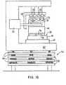
- the landing of the STM on the surface 39 of the specimencan be facilitated by the arrangement shown in Figure 9.
- the specimen 40is mounted on a holder 41 which rests on a base 42. Also attached to base 42 is a conventional xyz-drive module 43 which can be actuated to move an arm 44 in x- and y-directions as well as in vertical z-direction. Hanging from arm 44 and supported on two rests 45 is a block 46 which carries chip 7 including tunnel tip 18 and its supporting structure. When block 46 is properly adjusted over specimen 40, xyz-drive module 43 will lower block 46 until the feet 36... 38 touch the surface 39 of the specimen. Arm 44 can be lowered such that no physical contact between block 46 and arm 44 exists any longer, except for the electrical wires 47 which can be made very thin because of the small currents to be conducted. The number of wires required can be kept smaller than the number of functions performed by the STM if appropriate decoding is available on chip 7.
- the wires 47are replaced by optoelectronic connections.
- Arm 44carries a support 48 on which the required light emitting diodes 49 and photodetectors 50 are arranged. Their respective counterparts 51 and 52 are mounted on top of block 46. Fins 53 prevent cross-talk and provide cooling.
- the optoelectronic bridgefollows the motion of arm 44 and remains fixed after disconnection of arm 44 from block 46.
- arm 44positions block 46 over the specimen 40 by coarse selection of that part of the surface 39 thereof that is to be investigated, the positioning being controlled by xyz-drive module 43.
- a potential applied at contacts 25 and 26( Figure 5e) will cause an electric field between layers 19 and 21 and thus bending of tongue 17 towards layer 19.
- arm 44When tip 18 has arrived over the selected surface area, arm 44 will lower, placing blocks 46 with its feet 36 through 38 on the surface 39 of specimen 40. With a potential applied between tip 18, via contact 27, and the surface 39 of specimen 40, a tunnel current will flow provided the distance between tip 18 and surface 39 is in the neighbourhood of one nanometer. Reaching that distance is accomplished by slowly reducing the potential at contacts 25 and 26 so that tongue 17 is allowed to bend outwardly from layer 19.
- the entire scanning tunneling microscopeis arranged on top of a vibration filter 54 comprising a set of metal plates 55 separated by elastic pads 56 as it is known from IBM Technical Disclosure Bulletin Vol. 27, No. 5, p. 3137.
Landscapes
- Physics & Mathematics (AREA)
- Health & Medical Sciences (AREA)
- General Health & Medical Sciences (AREA)
- General Physics & Mathematics (AREA)
- Nuclear Medicine, Radiotherapy & Molecular Imaging (AREA)
- Radiology & Medical Imaging (AREA)
- Chemical & Material Sciences (AREA)
- Analytical Chemistry (AREA)
- Measurement Of Length, Angles, Or The Like Using Electric Or Magnetic Means (AREA)
- Electrostatic, Electromagnetic, Magneto- Strictive, And Variable-Resistance Transducers (AREA)
Description
- This invention relates to a scanning tunneling microscope of the type where a sharply pointed tip is maintained at a constant distance from a specimen to be investigated, and wherein the variations of the tunnel current occurring as the tip is raster-scanned across the surface of specimen are employed to adjust said distance and to control a plotter or other recording device for generating an image of the specimen's topography.
- Scanning tunneling microscopes of this sort are well known in the art, e.g. from US―A―4,343,993. Such scanning tunneling microscopes (hereafter for convenience abbreviated STM) comprise a fine, electrically conducting tip, means for positioning a conductive specimen surface sufficiently close to said conductive tip so that a tunnel current flows, means for scanning said tip across the specimen's surfaces, means for automatically controlling the separation distance between said tip and the specimen surface while the tip is scanned across the surface in response to the measured tunnel effect, and means for graphically displaying the spatial coordinates of said scanning tip to produce a topological map of said surface.
- For the positioning of the specimen with respect to the tip, several solutions have been proposed. One of these . is described in EP-Al-0071666. A plate of piezo-electric material rests on three feet which may be selectively clamped to a bench surface by means of electrostatic forces. By appropriate application of potentials to the plate and by selectively clamping and releasing the feet, displacement of the specimen resting on said plate in any direction is possible.
- While the travelling support of EP-A1-0071666 is useful for coarse positioning of the tip versus the specimen, fine positioning can be achieved with a known piezoelectric drive having three legs each associated with one coordinate and with the tunneling tip fixed at the joint of the three legs, cf. IBM Technical Disclosure Bulletin Vol. 27, No. 10B, (1985), p. 5976.
- The distance between tip and specimen for a tunnel current to flow must be of the order of 1 nanometer. Of course, at such small distances, the surface roughness at the specimen will cause frequent variations which have to be adjusted. The adjustment current is used to control a graphics display or recorder to which the coordinates of the current scanning position are also supplied.
- With a tip having a radius of curvature of ca. 1 nm, and with scanning steps in the subnanometer range, a resolution of the surface of the specimen down to the atomic level can be achieved. As will be immediately apparent to those skilled in the art, the slightest vibration affecting the tunneling region will disturb the measurements. Variation attenuation devices have already been described for use in connection with the STM, namely in EP-A1-0100785 and in IBM Technical Disclosure Bulletin Vol. 27 (1984), No. 5, p. 3137.
- As can be seen from a review of the state of the art as outlined above, the STM and all of its parts and aggregates are designed as rather bulky devices, i.e. they have large dimensions (several centimeters) and, hence, both a relatively large mass and relatively low stiffness, (for example, a low bending stiffness proportional to the third power of the length) which results in a low resonance frequency. Since the vibrations occurring in any environment have a low frequency, it is desirable for vibration-sensitive apparatus to have a high resonance frequency. The best way of increasing the resonance frequency of a given design is to reduce its dimensions.
- It is, therefore, an object of the present invention to propose a scanning tunneling microscope which is of small design and very stiff construction and which does not show the disadvantages of the prior art scanning tunneling microscopes, thus permitting even higher resolution.
- Another important aspect is that because of their design, prior art scanning tunneling microscopes need high operating voltages and are expensive to fabricate. They require high- grain voltage amplifiers which further add to the price. The STM of the present invention is easy and cheap to manufacture and operates at low voltages. It really opens an avenue to mass- production. The solution offered herein lies in the design of the STM in the so-called silicon micromachining technique, i.e. the essential parts of the STM are implemented on a tiny silicon ship using micromechanical techniques which are per se known in the art.
- An overview of the silicon micromachining art may be gained from an article by J. B. Angell, S. C. Terry and P. W. Barth, Silicon Micromechanical Devices, Scientific American, Vol. 248, No. 4, April 1983, pp. 36-47. While silicon has become familiar as the material from which electronic circuits, in particular integrated circuits, are fabricated, with widely publicized electrical properties, its mechanical properties, though highly interesting, have remained largely unnoticed.
- The silicon employed in the electronics industry takes the form of single crystals which are grown from a melt and sliced into disk-shaped wafers from 0,2 to 0,5 mm thick. The homogeneous crystal structure of the material gives it the electrical properties needed in microelectronic circuits. Yet, silicon in this form also has desirable mechanical properties. Silicon has its position in the periodic system directly below carbon and forms the same type of crystal as diamond. Single-crystal silicon is brittle and can be cleaved like diamond, but it is harder than most metals; it is extremely resistant to mechanical stress, it has a higher elastic limit in both, tension and compression than steel. And most important in connection with the STM of the present invention, single-crystal silicon remains strong under repeated cycles of tension and compression, whereas polycrystalline metals tend to weaken and break because stresses accumulate at the intercrystal boundaries.
- These and other'properties combined with the tremendous expertise acquired in processing electronic components made of silicon make this material very well suited for the design of a scanning tunneling microscope.
- Accordingly, the scanning tunneling microscope of the present invention, comprising at least one electron-emitting tip maintained at an essentially constant distance shorter than about 2 nm from the surface of a specimen to be investigated, an xy-drive for scanning said tip in a matrix fashion across said surface, and comprising means for controlling and displaying and/or recording the variations of the tunnel current and/ or the current required to maintain said distance essentially constant, thereby generating an image of the specimen's surface, is characterized in that said xy-drive consists of a semiconductor chip having a center portion connected by an intermediate portion and by two pairs of strips acting as leaf springs, to the main body of said chip, that said electron-emitting tip sits on a tongue forming an integral part of said center portion and being capable of being moved in a z-direction normal to the plane of said chip.
- The invention further relates to a method for manufacturing a scanning tunneling microscope of the type described above, the method being characterized by the steps of preparing a <110> oriented semiconductor chip, etching a four-sided portion at the center of said chip, which is linked by an intermediate portion and by two pairs of strips acting as leaf springs, to the main body of said chip, the slots between said strips and said center portion and said intermediate portion respectively being made parallel to the [111] and [1-11] directions of the semiconductor material of said chip, rendering selected parts of the vertical walls of said chip, said portions and said strips electrically conductive by doping said parts prior to etching and/or by depositing a metal layer thereon, underetching the area of said center portion of said chip supposed to carry said tip by using boron-doped layers, thus forming at least one tongue, growing a semiconductor platelet on said tongue, underetching said platelet to form said tip, and rendering said tip conductive by doping and/or coating with a film of conductive material.
- Details of embodiments of the invention will hereafter be described, by way of example, with reference to the drawings in which:
- Figure 1 is a top plan view of a semiconductor chip into which the scanning tunneling microscope of the present invention is formed;
- Figure 2 is a detail of the xy-drive of the STM of Figure 1;
- Figure 3 is a top plan view of a STM favorably aligned with regard to crystal orientation on a <110> semiconductor chip;
- Figure 4 is a cross-section of the STM along line A-A of Figure 1;
- Figure 5 in steps (a) through (e) shows the manufacture of the semiconductor chip for the STM;
- Figure 6 shows the placement of a resonant gate transistor on the semiconductor chip of the STM;
- Figure 7 shows the arrangement of the STM chip on a larger wafer;
- Figure 8 is a side view of the wafer of Figure 7;
- Figure 9 shows the STM wafer combined with a xyz-drive module for coarse positioning;
- Figure 10 shows the STM combined with optoelectronic signal transmission means and supported on a vibration filter.
- The heart of a scanning tunneling microscope is the tunnel tip with its xyz-drive which performs the scanning of the tip across the specimen and at the same time maintains the distance of the tip from the surface of the specimen within tight limits. Figure 1 shows an embodiment of the scanning mechanism and distance control. An essentially
square portion 1 is linked by a first pair of strips 2 and 3 to an L-shapedportion 4, and the latter in turn is linked by a second pair ofstrips chip 7 which appears as if surrounding the combination of said square and L-shapedportions assembly comprising elements 1 through 7 is one piece, the slots between the elements having been created by etching. - Starting from a
closed chip 7, a firsthorseshoeshaped slot 8 and a second, smaller and oppositely oriented,rectangular slot 10 are etched through the entire thickness of chip 7 (which may be e.g. between 0,05 and 0,3 mm thick), leaving betweenslots parallel strips structure encompassing elements 1 through 4 to oscillate in a direction orthogonal with respect to the length of the strips. This direction may be called the x-direction. - A
third slot 11 extending insideslot 10 is etched betweenportions portion 1 to oscillate in a direction orthogonal with respect to the x-direction, hence the y-direction. As a result of this,square portion 1 can be displaced in x and y directions with respect tochip 7. The positive x-and y-directions are assumed to point from thecenter area 4 towardsstrips 2 and 6, respectively. The driving force for the bending ofstrips strip 5, for example, by means ofelectrodes 12 through 15,electrodes electrodes electrodes area 4 in the negative x-direction. Application of voltage across the respective electrode area atstrip 6 causes motion in the positive x-direction. - Because of the small width of strips 2, 3; 5, 6 and
slots 8 ... 11 of about 8 micrometers each-which is easy to fabricate with state of the art lithography and etching, it is possible to achieve excursions ofportion 1 in x- and y-directions with respect tostationary chip 7 of sufficient amplitude for scanning purposes, with modest voltages. For example, with a strip length of 400 µm, slot width of 8 pm, strip width of 8 pm, an excursion of ±0,6 pm can be achieved with a potential of ±50V. With an original chip thickness of 300 µm and a thinned-downcenter portion 1 to about 30 pm, the lowest resonance frequency of the structure of Figure 1, which is mainly determined by the bending of thestrips - Essential in the implementation of the structure of Figure 1 are, of course, the etching of the narrow strips as well as rendering the sidewalls of
slots 8 ... 11 sufficiently conductive. One possibility is to use a <110> oriented silicon chip and make the slots parallel to the [111] and [1-11] directions of the single crystal silicon. This requires the replacement of the rectangular structure of Figure 1 by a 70,5° parallelogram structure as shown in Figure 3. The functioning of this structure is the same as that of the Figure 1 device, but the advantage is that anisotropic etching creates the required vertical walls in a simple and natural way. - Conductivity of the vertical walls of
slots 8 ... 11 can be achieved by doping the strips and their opposing areas appropriately priorto etching. This is advantageously done by thermomigration of liquid eutectic Al/Si alloy droplets through the singlecrystal silicon chip 7, as known from work by H. E. Cline and T. R. Anthony, High-Speed Droplet Migration in Silicon, Journ. Appl. Phys. 47 (1976) p. 2325. Alternatively, a metal layer can be deposited on each of the sidewalls by electroplating or sputtering,-with appropriate masking of the remainder of the chip during this process. - The tunnel tip in the embodiment of Figure 1 is conceived as an integral part of
portion 1 ofchip 7. Cut intoportion 1 by means of etching is achannel 16 drawn horseshoe-like in Figure 1, which leaves atongue 17 at one end connected withportion 1, as shown in Figure 4 which is a cross-section throughchip 7 of Figure 1 along the line A-A.Tunnel tip 18 sits on the free end oftongue 17.Channel 16 extends all underneathtongue 17 making the latter a very thin membrane. Also, as mentioned before,portion 1 is reduced in thickness with respect to the remainder ofchip 7 by a factor of 10. (Incidentally, none of the figures herein is drawn to scale.) - If
chip 7 is assumed to consist of monocrystalline silicon, the necessary underetching for formingtongue 17 can be achieved by means of boron-doped layers. Figure 5 shows an example of a possible processing schedule. On top of the thinned center part ofportion 1 consisting of n-type silicon a boron-dopedlayer 19 is created by diffusion (Step a).Layer 19 is then buried under a first epitaxially grown n-type silicon film 20 on top of which another boron-dopedlayer 21 is generated (Step b).Layer 21 in turn is buried under asecond epitaxial layer 22. In the place where thetunnel tip 18 is later to be formed a SiO2 platelet 23 is grown (Step c). Next then-type silicon layer 22 is etched to open upchannel 16 andcavity 28 around and underneath boron-dopedlayer 21, and to form tunnel tip 18 (Step d). Finally, an insulating Si02 layer 24 is formed on top of boron-dopedlayer 21 and provided with appropriate openings to permit deposition ofmetal contacts layers - The thickness of the
second epitaxial layer 22 and of the Si02 platelet 23 (Step c) have to be chosen such that etching oftip 18 and ofchannel 16 as well as ofcavity 28 belowtongue 17 at least approximately take the same time. If that is not possible,tip 18 must be protected in an additional processing step.Tip 18 is the result of anisotropic etching. Its faces are oriented normal to the <111 > directions. Sincechip 7 in the embodiment being described is assumed to be <110> oriented, two of these directions are in the chip plane, e.g. the (110) plane, and the respective tip walls are vertical, cf.wall 29 in Figure 5(d). As will be clear to those skilled in the art,tip 18 is formed after the Si02 platelet 23 is underetched completely. Tip 18, being the result of etching the high-resistivityintrinsic silicon layer 22, has to be rendered conductive for the purposes of the STM. It can either be doped or covered with a conducting film of a material different from silicon. If desired, microtips may be formed at the apex oftip 18 by electroadsorption known in the art, e.g. of field ion microscopy. Obviously, a plurality oftongue 17/tip 18 arrangements can be manufactured side by side inportion 1 ofchip 7 so as to permit easy transfer from a worn-down tip to a fresh one. If the spacing between twotips 18 is made very small, it is possible to obtain differential data by scanning the specimen with both tips at the same time.- In addition to the movement of
tip 18 with respect to the specimen in x- and y-directions,tip 18 can be displaced in z-direction by applying a potential tocontacts cavity 28, since the boron-dopedlayers tongue 17 can be bent in dependence on the force of said field. - The dimensions of
tongue 17 are determined by various parameters such as sufficient stiffness to guarantee a high vibrational resonance frequency, and a resonable bending amplitude which, preferably should not exceed about 20% of the height ofcavity 28 underneathtongue 17, lest the electrostatic deflection of the tongue should become unstable. - For a contemplated deflection of 10 nmN for
tongue 17, and an assumed distance of 3 um betweentongue 17 andbase 42, the dimensions given in the table below apply:
- A particular advantage of the present embodiment is the possibility of incorporating electronic circuitry on
chip 7 using, for example, area 30 in Figure 1 to implement a transistor which transforms the high-impedance tunnel system into a low-impedance noise-insensitive current source. The deflection oftongue 17 can be controlled with a resonant gate field-effect transistor as known from H. C. Nathanson, W. E. Newell, R. A. Wick- strom and J. R. Davis, Jr., The Resonant Gate Transistor, IEEE Trans. on Electron Devices ED-14 (1967), p. 117. - Figure 6 shows the arrangement of a resonant gate transistor with the
tongue 17 extending over the channel region of the MOS transistor of whichsource 31 and drain 32 are embedded in apad 33 for insulation fromconductive layer 19. It will be clear to those skilled in the art that the manufacture ofpad 33 as well as ofsource 31 and drain 32 will have to occur between steps (a) and (b) of Figure 5.Tongue 17 serves as the gate electrode of the transistor. As a potential is applied betweentongue 17 andlayer 19 via theirrespective electrodes tongue 17 is electrostatically attracted to bend towardslayer 17, thereby effectively increasing the capacitance betweentongue 17 and the channel region of the transistor. This change in capacitance results in a variation of the channel potential and a consequent alteration of the current through the transistor. - Figure 7 shows the integration of
chip 7 in awafer 34 which is for example shown to have a square outline.Chip 7 occupies one corner ofwafer 34; it is surrounded by anarea 35 which protudes from the rest ofwafer 34 as shown in the side view of Figure 8. With itsfeet wafer 34 rests on thesurface 39 of the specimen to be investigated. The height offoot 38 is adjusted so as to exceed that of tip 18-whentongue 17 is undeflected, by about 0,1 micrometer,feet foot 38 with the allowance of large tolerances because of their large distance fromtip 18. - To bring the STM into position,
wafer 34 can simply be placed on the specimen,feet 36 through 38 will prevent any damaging oftip 18. However, as this is not a trivial step, particularly in a vacuum environment, the landing of the STM on thesurface 39 of the specimen can be facilitated by the arrangement shown in Figure 9. - The
specimen 40 is mounted on aholder 41 which rests on abase 42. Also attached tobase 42 is a conventional xyz-drive module 43 which can be actuated to move anarm 44 in x- and y-directions as well as in vertical z-direction. Hanging fromarm 44 and supported on two rests 45 is ablock 46 which carrieschip 7 includingtunnel tip 18 and its supporting structure. Whenblock 46 is properly adjusted overspecimen 40, xyz-drive module 43 will lower block 46 until thefeet 36... 38 touch thesurface 39 of the specimen.Arm 44 can be lowered such that no physical contact betweenblock 46 andarm 44 exists any longer, except for the electrical wires 47 which can be made very thin because of the small currents to be conducted. The number of wires required can be kept smaller than the number of functions performed by the STM if appropriate decoding is available onchip 7. - In the embodiment shown in Figure 10, the wires 47 are replaced by optoelectronic connections.
Arm 44 carries asupport 48 on which the requiredlight emitting diodes 49 andphotodetectors 50 are arranged. Theirrespective counterparts 51 and 52 are mounted on top ofblock 46.Fins 53 prevent cross-talk and provide cooling. In this embodiment, the optoelectronic bridge follows the motion ofarm 44 and remains fixed after disconnection ofarm 44 fromblock 46. - Still referring to Figure 10, in operation,
arm 44 positions block 46 over thespecimen 40 by coarse selection of that part of thesurface 39 thereof that is to be investigated, the positioning being controlled by xyz-drive module 43. A potential applied atcontacts 25 and 26 (Figure 5e) will cause an electric field betweenlayers tongue 17 towardslayer 19. - When
tip 18 has arrived over the selected surface area,arm 44 will lower, placing blocks 46 with itsfeet 36 through 38 on thesurface 39 ofspecimen 40. With a potential applied betweentip 18, viacontact 27, and thesurface 39 ofspecimen 40, a tunnel current will flow provided the distance betweentip 18 andsurface 39 is in the neighbourhood of one nanometer. Reaching that distance is accomplished by slowly reducing the potential atcontacts tongue 17 is allowed to bend outwardly fromlayer 19. - To scan
tip 18 across thesurface 39 in a matrix fashion, appropriate potentials are applied atelectrodes 12 through 15 (Figure 2) controlling the positions ofportions chip 7. This scanning action, of course, occurs in a stepwise fashion such that each matrix point at whichtip 18 is halted can be associated with a particular voltage required to maintain the tunnel current (and with it thedistance tip 18/surface 39) at a predetermined value. Matrix position and value of adjustment voltage, if properly correlated, permit the generation of an image of the topography of the surface area scanned, as is well known in the art from US-A-4,343,993 mentioned before. - As also shown in Figure 10, the entire scanning tunneling microscope is arranged on top of a
vibration filter 54 comprising a set ofmetal plates 55 separated byelastic pads 56 as it is known from IBM Technical Disclosure Bulletin Vol. 27, No. 5, p. 3137.

Claims (11)
Priority Applications (7)
| Application Number | Priority Date | Filing Date | Title |
|---|---|---|---|
| DE8585102554TDE3572030D1 (en) | 1985-03-07 | 1985-03-07 | Scanning tunneling microscope |
| EP85102554AEP0194323B1 (en) | 1985-03-07 | 1985-03-07 | Scanning tunneling microscope |
| JP60271734AJPH0690005B2 (en) | 1985-03-07 | 1985-12-04 | Scanning tunnel effect microscope |
| CA000499457ACA1252918A (en) | 1985-03-07 | 1986-01-13 | Scanning tunneling microscope |
| US06/836,274US4668865A (en) | 1985-03-07 | 1986-03-05 | Scanning tunneling microscope |
| ES552715AES8707021A1 (en) | 1985-03-07 | 1986-03-06 | Scanning tunneling microscope. |
| ES557154AES8802105A1 (en) | 1985-03-07 | 1986-10-30 | Scanning tunneling microscope. |
Applications Claiming Priority (1)
| Application Number | Priority Date | Filing Date | Title |
|---|---|---|---|
| EP85102554AEP0194323B1 (en) | 1985-03-07 | 1985-03-07 | Scanning tunneling microscope |
Publications (2)
| Publication Number | Publication Date |
|---|---|
| EP0194323A1 EP0194323A1 (en) | 1986-09-17 |
| EP0194323B1true EP0194323B1 (en) | 1989-08-02 |
Family
ID=8193351
Family Applications (1)
| Application Number | Title | Priority Date | Filing Date |
|---|---|---|---|
| EP85102554AExpiredEP0194323B1 (en) | 1985-03-07 | 1985-03-07 | Scanning tunneling microscope |
Country Status (6)
| Country | Link |
|---|---|
| US (1) | US4668865A (en) |
| EP (1) | EP0194323B1 (en) |
| JP (1) | JPH0690005B2 (en) |
| CA (1) | CA1252918A (en) |
| DE (1) | DE3572030D1 (en) |
| ES (2) | ES8707021A1 (en) |
Families Citing this family (89)
| Publication number | Priority date | Publication date | Assignee | Title |
|---|---|---|---|---|
| USRE33387E (en)* | 1985-11-26 | 1990-10-16 | International Business Machines Corporation | Atomic force microscope and method for imaging surfaces with atomic resolution |
| EP0252745A3 (en)* | 1986-07-11 | 1990-01-24 | AGENCY OF INDUSTRIAL SCIENCE & TECHNOLOGY MINISTRY OF INTERNATIONAL TRADE & INDUSTRY | Relative displacement control apparatus |
| EP0262253A1 (en)* | 1986-10-03 | 1988-04-06 | International Business Machines Corporation | Micromechanical atomic force sensor head |
| EP0555941B1 (en)* | 1986-12-24 | 1997-07-30 | Canon Kabushiki Kaisha | Recording device and reproducing device |
| US4800274A (en)* | 1987-02-02 | 1989-01-24 | The Regents Of The University Of California | High resolution atomic force microscope |
| JPS63238503A (en)* | 1987-03-27 | 1988-10-04 | Jeol Ltd | Chip scanning device in scanning tunneling microscope |
| JPS63304103A (en)* | 1987-06-05 | 1988-12-12 | Hitachi Ltd | scanning surface microscope |
| EP0309236B1 (en)* | 1987-09-24 | 1994-07-06 | Canon Kabushiki Kaisha | Microprobe, preparation thereof and electronic device by use of said microprobe |
| US5255258A (en)* | 1987-09-24 | 1993-10-19 | Canon Kabushiki Kaisha | Microprobe, preparation thereof and electronic device by use of said microprobe |
| JP2553661B2 (en)* | 1987-09-24 | 1996-11-13 | キヤノン株式会社 | Microprog and method of manufacturing the same |
| EP0566214B1 (en)* | 1987-09-24 | 1999-05-26 | Canon Kabushiki Kaisha | Microprobe |
| US4868396A (en)* | 1987-10-13 | 1989-09-19 | Arizona Board Of Regents, Arizona State University | Cell and substrate for electrochemical STM studies |
| JPH06105262B2 (en)* | 1987-11-27 | 1994-12-21 | セイコー電子工業株式会社 | Method and apparatus for electrochemical measurement and simultaneous measurement of tunnel current |
| US4906840A (en)* | 1988-01-27 | 1990-03-06 | The Board Of Trustees Of Leland Stanford Jr., University | Integrated scanning tunneling microscope |
| JP2577423B2 (en)* | 1988-02-29 | 1997-01-29 | 工業技術院長 | Large-stroke scanning tunneling microscope |
| JP2594452B2 (en)* | 1988-03-04 | 1997-03-26 | 日本電信電話株式会社 | Surface profile measuring device |
| US4841148A (en)* | 1988-03-21 | 1989-06-20 | The Board Of Trustees Of The University Of Illinois | Variable temperature scanning tunneling microscope |
| GB8818445D0 (en)* | 1988-08-03 | 1988-09-07 | Jones B L | Stm probe |
| JPH0275902A (en)* | 1988-09-13 | 1990-03-15 | Seiko Instr Inc | Diamond probe and its forming method |
| JP2896794B2 (en)* | 1988-09-30 | 1999-05-31 | キヤノン株式会社 | Scanning tunnel current detector, scanning tunnel microscope, and recording / reproducing device |
| US5220555A (en)* | 1988-09-30 | 1993-06-15 | Canon Kabushiki Kaisha | Scanning tunnel-current-detecting device and method for detecting tunnel current and scanning tunnelling microscope and recording/reproducing device using thereof |
| DE3850968T2 (en)* | 1988-10-14 | 1995-03-16 | Ibm | Distance-controlled tunnel effect converter and memory unit using the converter with direct access. |
| US5210714A (en)* | 1988-10-14 | 1993-05-11 | International Business Machines Corporation | Distance-controlled tunneling transducer and direct access storage unit employing the transducer |
| JP2547869B2 (en)* | 1988-11-09 | 1996-10-23 | キヤノン株式会社 | PROBE UNIT, METHOD FOR DRIVING THE PROBE, AND SCANNING TUNNEL CURRENT DETECTION DEVICE HAVING THE PROBE UNIT |
| JPH02134503A (en)* | 1988-11-15 | 1990-05-23 | Mitsubishi Electric Corp | Scanning type tunnel microscope |
| US4943719A (en)* | 1989-01-17 | 1990-07-24 | The Board Of Trustees Of The Leland Stanford University | Microminiature cantilever stylus |
| JP2834173B2 (en)* | 1989-02-17 | 1998-12-09 | 株式会社日立製作所 | Scanning tunnel acoustic microscope |
| US4942299A (en)* | 1989-03-01 | 1990-07-17 | Midwest Research Institute | Method and apparatus for differential spectroscopic atomic-imaging using scanning tunneling microscopy |
| US4941753A (en)* | 1989-04-07 | 1990-07-17 | International Business Machines Corp. | Absorption microscopy and/or spectroscopy with scanning tunneling microscopy control |
| US4925139A (en)* | 1989-04-28 | 1990-05-15 | International Business Machines Corporation | Mechanical stage support for a scanning tunneling microscope |
| JPH02295050A (en)* | 1989-05-09 | 1990-12-05 | Olympus Optical Co Ltd | Apparatus and method for circuit pattern formation using mu-stm |
| JPH02311702A (en)* | 1989-05-29 | 1990-12-27 | Olympus Optical Co Ltd | Scanning type tunnel microscope apparatus |
| US5015850A (en)* | 1989-06-20 | 1991-05-14 | The Board Of Trustees Of The Leland Stanford Junior University | Microfabricated microscope assembly |
| US5075548A (en)* | 1989-07-17 | 1991-12-24 | Olympus Optical Co., Ltd. | Tunnel current probe moving mechanism having parallel cantilevers |
| US4992659A (en)* | 1989-07-27 | 1991-02-12 | International Business Machines Corporation | Near-field lorentz force microscopy |
| EP0413042B1 (en)* | 1989-08-16 | 1992-12-16 | International Business Machines Corporation | Method of producing micromechanical sensors for the afm/stm profilometry and micromechanical afm/stm sensor head |
| US5206702A (en)* | 1989-10-09 | 1993-04-27 | Olympus Optical Co., Ltd. | Technique for canceling the effect of external vibration on an atomic force microscope |
| US5126574A (en)* | 1989-10-10 | 1992-06-30 | The United States Of America As Represented By The Secretary Of Commerce | Microtip-controlled nanostructure fabrication and multi-tipped field-emission tool for parallel-process nanostructure fabrication |
| US5021364A (en)* | 1989-10-31 | 1991-06-04 | The Board Of Trustees Of The Leland Stanford Junior University | Microcantilever with integral self-aligned sharp tetrahedral tip |
| USRE36603E (en)* | 1989-10-13 | 2000-03-07 | International Business Machines Corp. | Distance-controlled tunneling transducer and direct access storage unit employing the transducer |
| US5021672A (en)* | 1989-12-22 | 1991-06-04 | E. I. Du Pont De Nemours And Company | Etching of nanoscale structures |
| US5253515A (en)* | 1990-03-01 | 1993-10-19 | Olympus Optical Co., Ltd. | Atomic probe microscope and cantilever unit for use in the microscope |
| US5055680A (en)* | 1990-04-03 | 1991-10-08 | Lk Technologies, Inc. | Scanning tunneling microscope |
| JP2624873B2 (en)* | 1990-05-16 | 1997-06-25 | 松下電器産業株式会社 | Atomic force microscope probe and method of manufacturing the same |
| EP0468071B1 (en)* | 1990-07-25 | 1994-09-14 | International Business Machines Corporation | Method of producing micromechanical sensors for the AFM/STM/MFM profilometry and micromechanical AFM/STM/MFM sensor head |
| US5163328A (en)* | 1990-08-06 | 1992-11-17 | Colin Electronics Co., Ltd. | Miniature pressure sensor and pressure sensor arrays |
| JP3030574B2 (en)* | 1990-08-16 | 2000-04-10 | キヤノン株式会社 | Micro-displacement information detecting probe element, scanning tunnel microscope, atomic force microscope, and information processing apparatus using the same |
| US5047649A (en)* | 1990-10-09 | 1991-09-10 | International Business Machines Corporation | Method and apparatus for writing or etching narrow linewidth patterns on insulating materials |
| DE69023347T2 (en)* | 1990-12-21 | 1996-05-30 | International Business Machines Corp., Armonk, N.Y. | Integrated scanning tunneling microscope with pneumatic and electrostatic control and method for producing the same. |
| US5283437A (en)* | 1990-12-21 | 1994-02-01 | International Business Machines Corporation | Pneumatically and electrostatically driven scanning tunneling microscope |
| JP3010318B2 (en)* | 1991-02-26 | 2000-02-21 | キヤノン株式会社 | Micro probe, method of manufacturing the same, surface observation device and information processing device using the probe |
| US5235187A (en)* | 1991-05-14 | 1993-08-10 | Cornell Research Foundation | Methods of fabricating integrated, aligned tunneling tip pairs |
| JP3198355B2 (en)* | 1991-05-28 | 2001-08-13 | キヤノン株式会社 | Small displacement element, scanning tunnel microscope using the same, and information processing apparatus |
| JP3148946B2 (en)* | 1991-05-30 | 2001-03-26 | キヤノン株式会社 | Probe driving mechanism, tunnel current detecting device using the mechanism, information processing device, piezoelectric actuator |
| US5606162A (en)* | 1991-06-13 | 1997-02-25 | British Technology Group Limited | Microprobe for surface-scanning microscopes |
| US5155361A (en)* | 1991-07-26 | 1992-10-13 | The Arizona Board Of Regents, A Body Corporate Acting For And On Behalf Of Arizona State University | Potentiostatic preparation of molecular adsorbates for scanning probe microscopy |
| US5319961A (en)* | 1991-09-17 | 1994-06-14 | Olympus Optical Co., Ltd. | Cantilever chip for use in scanning probe microscope |
| JP3184619B2 (en)* | 1991-09-24 | 2001-07-09 | キヤノン株式会社 | Parallel plane holding mechanism and memory device and STM device using the same |
| US5298975A (en)* | 1991-09-27 | 1994-03-29 | International Business Machines Corporation | Combined scanning force microscope and optical metrology tool |
| US5763782A (en)* | 1992-03-16 | 1998-06-09 | British Technology Group Limited | Micromechanical sensor |
| US5179499A (en)* | 1992-04-14 | 1993-01-12 | Cornell Research Foundation, Inc. | Multi-dimensional precision micro-actuator |
| US5267471A (en)* | 1992-04-30 | 1993-12-07 | Ibm Corporation | Double cantilever sensor for atomic force microscope |
| JP3029499B2 (en)* | 1992-05-07 | 2000-04-04 | キヤノン株式会社 | Recording and playback device |
| US5287082A (en)* | 1992-07-02 | 1994-02-15 | Cornell Research Foundation, Inc. | Submicron isolated, released resistor structure |
| JP3402661B2 (en)* | 1992-07-06 | 2003-05-06 | キヤノン株式会社 | Cantilever probe and information processing apparatus using the same |
| US5399415A (en)* | 1993-02-05 | 1995-03-21 | Cornell Research Foundation, Inc. | Isolated tungsten microelectromechanical structures |
| JP3054900B2 (en)* | 1993-03-10 | 2000-06-19 | セイコーインスツルメンツ株式会社 | Micro processing equipment |
| DE4309206C1 (en)* | 1993-03-22 | 1994-09-15 | Texas Instruments Deutschland | Semiconductor device having a force and/or acceleration sensor |
| US5536988A (en)* | 1993-06-01 | 1996-07-16 | Cornell Research Foundation, Inc. | Compound stage MEM actuator suspended for multidimensional motion |
| US5440920A (en)* | 1994-02-03 | 1995-08-15 | Molecular Imaging Systems | Scanning force microscope with beam tracking lens |
| US5515719A (en)* | 1994-05-19 | 1996-05-14 | Molecular Imaging Corporation | Controlled force microscope for operation in liquids |
| US5513518A (en)* | 1994-05-19 | 1996-05-07 | Molecular Imaging Corporation | Magnetic modulation of force sensor for AC detection in an atomic force microscope |
| US5753814A (en)* | 1994-05-19 | 1998-05-19 | Molecular Imaging Corporation | Magnetically-oscillated probe microscope for operation in liquids |
| US5866805A (en)* | 1994-05-19 | 1999-02-02 | Molecular Imaging Corporation Arizona Board Of Regents | Cantilevers for a magnetically driven atomic force microscope |
| JP3192887B2 (en)* | 1994-09-21 | 2001-07-30 | キヤノン株式会社 | Probe, scanning probe microscope using the probe, and recording / reproducing apparatus using the probe |
| EP0772876A1 (en)* | 1995-04-29 | 1997-05-14 | International Business Machines Corporation | Micromechanically manufactured read/write head for charge coupled devices |
| US5717631A (en)* | 1995-07-21 | 1998-02-10 | Carnegie Mellon University | Microelectromechanical structure and process of making same |
| US5834864A (en)* | 1995-09-13 | 1998-11-10 | Hewlett Packard Company | Magnetic micro-mover |
| JP3576677B2 (en)* | 1996-01-19 | 2004-10-13 | キヤノン株式会社 | Electrostatic actuator, probe using the actuator, scanning probe microscope, processing device, recording / reproducing device |
| JP2925114B2 (en)* | 1996-07-22 | 1999-07-28 | 株式会社日立製作所 | measuring device |
| FR2755224B1 (en)* | 1996-10-24 | 1998-12-04 | Suisse Electronique Microtech | SENSOR WITH TUNNEL EFFECT, PARTICULARLY FOR RAISING THE TOPOGRAPHY OF A SURFACE |
| US6088320A (en)* | 1997-02-19 | 2000-07-11 | International Business Machines Corporation | Micro-mechanically fabricated read/write head with a strengthening shell on the tip shaft |
| US7156965B1 (en) | 2001-11-09 | 2007-01-02 | Veeco Instruments Inc. | Scanning electrochemical potential microscope |
| DE10155930B4 (en)* | 2001-11-14 | 2020-09-24 | Nano Analytik Gmbh | Field effect transistor sensor |
| JP3755460B2 (en)* | 2001-12-26 | 2006-03-15 | ソニー株式会社 | Electrostatically driven MEMS element and manufacturing method thereof, optical MEMS element, light modulation element, GLV device, laser display, and MEMS apparatus |
| SG101537A1 (en)* | 2002-06-03 | 2004-01-30 | Sensfab Pte Ltd | Method of forming atomic force microscope tips |
| US20050128927A1 (en)* | 2003-12-15 | 2005-06-16 | Hewlett-Packard Development Co., L.P. | Electrostatic actuator for contact probe storage device |
| KR100790893B1 (en)* | 2006-10-20 | 2008-01-03 | 삼성전자주식회사 | Semiconductor probe with convex resistive tip and manufacturing method |
| KR102374926B1 (en)* | 2017-08-25 | 2022-03-16 | 주식회사 히타치하이테크 | Calibration sample, electron beam adjustment method and electron beam device using the same |
Family Cites Families (4)
| Publication number | Priority date | Publication date | Assignee | Title |
|---|---|---|---|---|
| US4203128A (en)* | 1976-11-08 | 1980-05-13 | Wisconsin Alumni Research Foundation | Electrostatically deformable thin silicon membranes |
| CH643397A5 (en)* | 1979-09-20 | 1984-05-30 | Ibm | GRID TUNNEL MICROSCOPE. |
| EP0071666B1 (en)* | 1981-08-10 | 1985-02-06 | International Business Machines Corporation | Electric travelling support |
| US4506154A (en)* | 1982-10-22 | 1985-03-19 | Scire Fredric E | Planar biaxial micropositioning stage |
- 1985
- 1985-03-07DEDE8585102554Tpatent/DE3572030D1/ennot_activeExpired
- 1985-03-07EPEP85102554Apatent/EP0194323B1/ennot_activeExpired
- 1985-12-04JPJP60271734Apatent/JPH0690005B2/ennot_activeExpired - Fee Related
- 1986
- 1986-01-13CACA000499457Apatent/CA1252918A/ennot_activeExpired
- 1986-03-05USUS06/836,274patent/US4668865A/ennot_activeExpired - Lifetime
- 1986-03-06ESES552715Apatent/ES8707021A1/ennot_activeExpired
- 1986-10-30ESES557154Apatent/ES8802105A1/ennot_activeExpired
Also Published As
| Publication number | Publication date |
|---|---|
| JPS61206148A (en) | 1986-09-12 |
| EP0194323A1 (en) | 1986-09-17 |
| ES552715A0 (en) | 1987-07-01 |
| ES8707021A1 (en) | 1987-07-01 |
| ES557154A0 (en) | 1988-03-16 |
| ES8802105A1 (en) | 1988-03-16 |
| DE3572030D1 (en) | 1989-09-07 |
| US4668865A (en) | 1987-05-26 |
| CA1252918A (en) | 1989-04-18 |
| JPH0690005B2 (en) | 1994-11-14 |
Similar Documents
| Publication | Publication Date | Title |
|---|---|---|
| EP0194323B1 (en) | Scanning tunneling microscope | |
| EP0478666B1 (en) | Microfabricated microscope assembly | |
| KR100748046B1 (en) | Electrical property evaluation device | |
| US5449903A (en) | Methods of fabricating integrated, aligned tunneling tip pairs | |
| US5475318A (en) | Microprobe | |
| US6066265A (en) | Micromachined silicon probe for scanning probe microscopy | |
| EP0475564A1 (en) | Fine scanning mechanism for atomic force microscope | |
| US20030183761A1 (en) | Scanning probe system with spring probe and actuation/sensing structure | |
| US7735357B2 (en) | SPM cantilever and manufacturing method thereof | |
| Akamine et al. | A planar process for microfabrication of a scanning tunneling microscope | |
| EP0880671A2 (en) | Microfabricated torsional cantilevers for sensitive force detection | |
| Joachim et al. | Multiple atomic scale solid surface interconnects for atom circuits and molecule logicgates | |
| US20050082598A1 (en) | Storage device with charge trapping structure and methods | |
| Anders et al. | Simple micropositioning devices for STM | |
| Heinzelmann et al. | Atomic force microscopy: General aspects and application to insulators | |
| JPH0721968A (en) | Cantilever type displacement element, cantilever type probe using the same, scanning probe microscope and information processing apparatus using the same | |
| EP3809143B1 (en) | A method for scanning probe microscopy | |
| JPH11271015A (en) | Cantilever tip for scanning probe microscope and its manufacture | |
| Toshiyoshi et al. | Fabrication of micromechanical tunneling probes and actuators on a silicon chip | |
| JP3234722B2 (en) | Arc-shaped warped lever type actuator, method of driving the actuator, and information processing apparatus using information input / output probe | |
| JP3114023B2 (en) | Manufacturing method of integrated actuator | |
| CA2031733C (en) | Method for forming probe and apparatus therefor | |
| JP2002154100A (en) | Fine processing device and fine processing method | |
| Lin et al. | Adhesion of Nanoscale Metal Clusters to Semiconductor Surfaces: A Scanning Tunneling Microscopy Examination | |
| JPH10206435A (en) | Method for producing probe and probe |
Legal Events
| Date | Code | Title | Description |
|---|---|---|---|
| PUAI | Public reference made under article 153(3) epc to a published international application that has entered the european phase | Free format text:ORIGINAL CODE: 0009012 | |
| AK | Designated contracting states | Kind code of ref document:A1 Designated state(s):CH DE FR GB IT LI NL SE | |
| 17P | Request for examination filed | Effective date:19870116 | |
| 17Q | First examination report despatched | Effective date:19881122 | |
| GRAA | (expected) grant | Free format text:ORIGINAL CODE: 0009210 | |
| AK | Designated contracting states | Kind code of ref document:B1 Designated state(s):CH DE FR GB IT LI NL SE | |
| REF | Corresponds to: | Ref document number:3572030 Country of ref document:DE Date of ref document:19890907 | |
| ITF | It: translation for a ep patent filed | ||
| ET | Fr: translation filed | ||
| PLBE | No opposition filed within time limit | Free format text:ORIGINAL CODE: 0009261 | |
| STAA | Information on the status of an ep patent application or granted ep patent | Free format text:STATUS: NO OPPOSITION FILED WITHIN TIME LIMIT | |
| 26N | No opposition filed | ||
| ITTA | It: last paid annual fee | ||
| EAL | Se: european patent in force in sweden | Ref document number:85102554.4 | |
| PGFP | Annual fee paid to national office [announced via postgrant information from national office to epo] | Ref country code:FR Payment date:19970304 Year of fee payment:13 | |
| PGFP | Annual fee paid to national office [announced via postgrant information from national office to epo] | Ref country code:SE Payment date:19980309 Year of fee payment:14 | |
| PGFP | Annual fee paid to national office [announced via postgrant information from national office to epo] | Ref country code:NL Payment date:19980330 Year of fee payment:14 | |
| PG25 | Lapsed in a contracting state [announced via postgrant information from national office to epo] | Ref country code:FR Free format text:THE PATENT HAS BEEN ANNULLED BY A DECISION OF A NATIONAL AUTHORITY Effective date:19980331 | |
| REG | Reference to a national code | Ref country code:FR Ref legal event code:ST | |
| PG25 | Lapsed in a contracting state [announced via postgrant information from national office to epo] | Ref country code:SE Free format text:LAPSE BECAUSE OF NON-PAYMENT OF DUE FEES Effective date:19990308 | |
| PG25 | Lapsed in a contracting state [announced via postgrant information from national office to epo] | Ref country code:NL Free format text:LAPSE BECAUSE OF NON-PAYMENT OF DUE FEES Effective date:19991001 | |
| EUG | Se: european patent has lapsed | Ref document number:85102554.4 | |
| NLV4 | Nl: lapsed or anulled due to non-payment of the annual fee | Effective date:19991001 | |
| EUG | Se: european patent has lapsed | Ref document number:85102554.4 | |
| REG | Reference to a national code | Ref country code:GB Ref legal event code:IF02 | |
| PGFP | Annual fee paid to national office [announced via postgrant information from national office to epo] | Ref country code:CH Payment date:20030625 Year of fee payment:19 | |
| PGFP | Annual fee paid to national office [announced via postgrant information from national office to epo] | Ref country code:GB Payment date:20040301 Year of fee payment:20 | |
| PGFP | Annual fee paid to national office [announced via postgrant information from national office to epo] | Ref country code:DE Payment date:20040322 Year of fee payment:20 | |
| PG25 | Lapsed in a contracting state [announced via postgrant information from national office to epo] | Ref country code:LI Free format text:LAPSE BECAUSE OF NON-PAYMENT OF DUE FEES Effective date:20040331 Ref country code:CH Free format text:LAPSE BECAUSE OF NON-PAYMENT OF DUE FEES Effective date:20040331 | |
| REG | Reference to a national code | Ref country code:CH Ref legal event code:PL | |
| PG25 | Lapsed in a contracting state [announced via postgrant information from national office to epo] | Ref country code:GB Free format text:LAPSE BECAUSE OF EXPIRATION OF PROTECTION Effective date:20050306 | |
| REG | Reference to a national code | Ref country code:GB Ref legal event code:PE20 |