EP0182198A2 - Single transistor electrically programmable device and method - Google Patents
Single transistor electrically programmable device and methodDownload PDFInfo
- Publication number
- EP0182198A2 EP0182198A2EP85114090AEP85114090AEP0182198A2EP 0182198 A2EP0182198 A2EP 0182198A2EP 85114090 AEP85114090 AEP 85114090AEP 85114090 AEP85114090 AEP 85114090AEP 0182198 A2EP0182198 A2EP 0182198A2
- Authority
- EP
- European Patent Office
- Prior art keywords
- layer
- source
- floating gate
- gate
- column
- Prior art date
- Legal status (The legal status is an assumption and is not a legal conclusion. Google has not performed a legal analysis and makes no representation as to the accuracy of the status listed.)
- Granted
Links
Images


Classifications
- H—ELECTRICITY
- H10—SEMICONDUCTOR DEVICES; ELECTRIC SOLID-STATE DEVICES NOT OTHERWISE PROVIDED FOR
- H10D—INORGANIC ELECTRIC SEMICONDUCTOR DEVICES
- H10D62/00—Semiconductor bodies, or regions thereof, of devices having potential barriers
- H10D62/10—Shapes, relative sizes or dispositions of the regions of the semiconductor bodies; Shapes of the semiconductor bodies
- H10D62/13—Semiconductor regions connected to electrodes carrying current to be rectified, amplified or switched, e.g. source or drain regions
- H10D62/149—Source or drain regions of field-effect devices
- H10D62/151—Source or drain regions of field-effect devices of IGFETs
- G—PHYSICS
- G11—INFORMATION STORAGE
- G11C—STATIC STORES
- G11C16/00—Erasable programmable read-only memories
- G11C16/02—Erasable programmable read-only memories electrically programmable
- G11C16/04—Erasable programmable read-only memories electrically programmable using variable threshold transistors, e.g. FAMOS
- G11C16/0408—Erasable programmable read-only memories electrically programmable using variable threshold transistors, e.g. FAMOS comprising cells containing floating gate transistors
- G11C16/0416—Erasable programmable read-only memories electrically programmable using variable threshold transistors, e.g. FAMOS comprising cells containing floating gate transistors comprising cells containing a single floating gate transistor and no select transistor, e.g. UV EPROM
- G—PHYSICS
- G11—INFORMATION STORAGE
- G11C—STATIC STORES
- G11C16/00—Erasable programmable read-only memories
- G11C16/02—Erasable programmable read-only memories electrically programmable
- G11C16/06—Auxiliary circuits, e.g. for writing into memory
- G11C16/10—Programming or data input circuits
- G—PHYSICS
- G11—INFORMATION STORAGE
- G11C—STATIC STORES
- G11C16/00—Erasable programmable read-only memories
- G11C16/02—Erasable programmable read-only memories electrically programmable
- G11C16/06—Auxiliary circuits, e.g. for writing into memory
- G11C16/10—Programming or data input circuits
- G11C16/14—Circuits for erasing electrically, e.g. erase voltage switching circuits
- G11C16/16—Circuits for erasing electrically, e.g. erase voltage switching circuits for erasing blocks, e.g. arrays, words, groups
- H—ELECTRICITY
- H01—ELECTRIC ELEMENTS
- H01L—SEMICONDUCTOR DEVICES NOT COVERED BY CLASS H10
- H01L21/00—Processes or apparatus adapted for the manufacture or treatment of semiconductor or solid state devices or of parts thereof
- H01L21/02—Manufacture or treatment of semiconductor devices or of parts thereof
- H01L21/04—Manufacture or treatment of semiconductor devices or of parts thereof the devices having potential barriers, e.g. a PN junction, depletion layer or carrier concentration layer
- H01L21/18—Manufacture or treatment of semiconductor devices or of parts thereof the devices having potential barriers, e.g. a PN junction, depletion layer or carrier concentration layer the devices having semiconductor bodies comprising elements of Group IV of the Periodic Table or AIIIBV compounds with or without impurities, e.g. doping materials
- H01L21/30—Treatment of semiconductor bodies using processes or apparatus not provided for in groups H01L21/20 - H01L21/26
- H01L21/31—Treatment of semiconductor bodies using processes or apparatus not provided for in groups H01L21/20 - H01L21/26 to form insulating layers thereon, e.g. for masking or by using photolithographic techniques; After treatment of these layers; Selection of materials for these layers
- H01L21/3205—Deposition of non-insulating-, e.g. conductive- or resistive-, layers on insulating layers; After-treatment of these layers
- H01L21/321—After treatment
- H—ELECTRICITY
- H10—SEMICONDUCTOR DEVICES; ELECTRIC SOLID-STATE DEVICES NOT OTHERWISE PROVIDED FOR
- H10B—ELECTRONIC MEMORY DEVICES
- H10B69/00—Erasable-and-programmable ROM [EPROM] devices not provided for in groups H10B41/00 - H10B63/00, e.g. ultraviolet erasable-and-programmable ROM [UVEPROM] devices
- H—ELECTRICITY
- H10—SEMICONDUCTOR DEVICES; ELECTRIC SOLID-STATE DEVICES NOT OTHERWISE PROVIDED FOR
- H10D—INORGANIC ELECTRIC SEMICONDUCTOR DEVICES
- H10D30/00—Field-effect transistors [FET]
- H10D30/01—Manufacture or treatment
- H10D30/021—Manufacture or treatment of FETs having insulated gates [IGFET]
- H10D30/0411—Manufacture or treatment of FETs having insulated gates [IGFET] of FETs having floating gates
- H—ELECTRICITY
- H10—SEMICONDUCTOR DEVICES; ELECTRIC SOLID-STATE DEVICES NOT OTHERWISE PROVIDED FOR
- H10D—INORGANIC ELECTRIC SEMICONDUCTOR DEVICES
- H10D30/00—Field-effect transistors [FET]
- H10D30/60—Insulated-gate field-effect transistors [IGFET]
- H10D30/68—Floating-gate IGFETs
- H10D30/681—Floating-gate IGFETs having only two programming levels
- H10D30/684—Floating-gate IGFETs having only two programming levels programmed by hot carrier injection
- H10D30/685—Floating-gate IGFETs having only two programming levels programmed by hot carrier injection from the channel
- H—ELECTRICITY
- H10—SEMICONDUCTOR DEVICES; ELECTRIC SOLID-STATE DEVICES NOT OTHERWISE PROVIDED FOR
- H10D—INORGANIC ELECTRIC SEMICONDUCTOR DEVICES
- H10D64/00—Electrodes of devices having potential barriers
- H10D64/01—Manufacture or treatment
- H10D64/031—Manufacture or treatment of data-storage electrodes
- H10D64/035—Manufacture or treatment of data-storage electrodes comprising conductor-insulator-conductor-insulator-semiconductor structures
- H—ELECTRICITY
- H10—SEMICONDUCTOR DEVICES; ELECTRIC SOLID-STATE DEVICES NOT OTHERWISE PROVIDED FOR
- H10D—INORGANIC ELECTRIC SEMICONDUCTOR DEVICES
- H10D64/00—Electrodes of devices having potential barriers
- H10D64/60—Electrodes characterised by their materials
- H10D64/66—Electrodes having a conductor capacitively coupled to a semiconductor by an insulator, e.g. MIS electrodes
- H10D64/68—Electrodes having a conductor capacitively coupled to a semiconductor by an insulator, e.g. MIS electrodes characterised by the insulator, e.g. by the gate insulator
- H10D64/681—Electrodes having a conductor capacitively coupled to a semiconductor by an insulator, e.g. MIS electrodes characterised by the insulator, e.g. by the gate insulator having a compositional variation, e.g. multilayered
- H—ELECTRICITY
- H10—SEMICONDUCTOR DEVICES; ELECTRIC SOLID-STATE DEVICES NOT OTHERWISE PROVIDED FOR
- H10D—INORGANIC ELECTRIC SEMICONDUCTOR DEVICES
- H10D64/00—Electrodes of devices having potential barriers
- H10D64/60—Electrodes characterised by their materials
- H10D64/66—Electrodes having a conductor capacitively coupled to a semiconductor by an insulator, e.g. MIS electrodes
- H10D64/68—Electrodes having a conductor capacitively coupled to a semiconductor by an insulator, e.g. MIS electrodes characterised by the insulator, e.g. by the gate insulator
- H10D64/693—Electrodes having a conductor capacitively coupled to a semiconductor by an insulator, e.g. MIS electrodes characterised by the insulator, e.g. by the gate insulator the insulator comprising nitrogen, e.g. nitrides, oxynitrides or nitrogen-doped materials
Definitions
- the present inventionis directed to an electrically programmable and erasable device and a method for making the same.
- the electrically programmable memory devicecan be of the type that is commonly called Electrically Erasable Programmable Read Only Memory (EEPROM). More particularly, the present invention relates to the structure and manufacture of a single transistor EEPROM cell suitable for use in high density memory devices.
- EEPROMElectrically Erasable Programmable Read Only Memory
- an EPROM or an EEPROMis characterized by a "floating gate” and an electrical connection termed a "control gate”, both of which are fabricated out of polycrystalline silicon doped with an appropriate doping material to render the polycrystalline conductive.
- a typical doping materialis phosphorus.
- the floating gateis separated from a substrate region by a gate oxide layer of insulating material.
- the substrate regionincludes symmetrical source and drain regions which define a channel.
- the floating gate and the control gateare separated by a layer of insulating material, typically silicon dioxide (Si0 2 ).
- insulating materialtypically silicon dioxide (Si0 2 ).
- the principle upon which the EPROM or EEPROM device operatesis that electrons, or charge, are stored on the "floating gate" in a capacitive manner.
- the dielectric layer between the floating gate and the control gateis important.
- the floating gateis formed by reacting SiH 4 in a low pressure chemical vapor deposition chamber and then doped with POC1 3 in a separate doping cycle.
- a layer of silicon dioxideis then deposited or thermally grown on the doped polycrystalline layer of silicon.
- the layer of silicon dioxideis typically approximately 750 angstroms.
- a high oxidation temperaturegreater than 1050 degrees C
- heavier phosphorus dopingare required to achieve better interpoly quality and breakdown capability.
- oxidation at high temperature on heavily-doped polysiliconinvolves several drawbacks, such as: (1) outgassing during interpoly oxidation which causes autodoping on the wafer; and (2) oxidation enhanced diffusion of phosphorus from the floating gate to the tunnel oxide, which forms trapping centers in the oxide.
- the electron trappingcollapses the threshold window EEPROM cell at 10 4 cycles.
- the second layer of doped polycrystalline siliconis formed on top of the insulating layer of S i0 2 .
- the typical write or erase voltagei.e., the voltage which is needed to place charge on or to remove charge from the floating gate, has been high, i.e., in excess of 20 volts. In turn, this places shrinkage limits on gate oxide thickness, junction depth and die size.
- Silicon nitride(Si 3 N 4 ) has also been used as an insulating layer of dual dielectric (thermal oxide with silicon nitride on it) between the floating gate and the control gate connection. Silicon nitride has the property that it is more dense than silicon dioxide and, therefore, affords higher capacitive coupling between the floating gate and the control gate.
- a typical dual dielectric between the floating gate and the control gateis composed of 500 angstroms oxide and 400 angstroms nitride.
- the write and erase voltageis still relatively high, in excess of 18 volts. High erase and program voltages for conventional EEPROM devices are of major concern. Such a requirement has led to the need for a separate high voltage supply when operating the devices, or for the use of special voltage multiplying circuitry within the device for boosting the supply voltage to the requisite program and erase levels.
- an electrically erasable programmable memory devicecomprising a body of single crystalline semiconductive material having a source and a drain, a first layer of insulating material positioned on the body, a floating gate positioned on the first layer of insulating material, a second layer of insulating material positioned on the floating gate, and a gate over the second layer of insulating material, wherein the source is formed of a deep region of a first material, such as phosphorous and a shallower region of a second material, such as arsenic and phosphorous, and the drain is formed of a shallow region of the second material, and further wherein a portion of a part of the deep region, such as arsenic only, underlies the first layer of insulating material and the first material is selected to optimize the junction overlap with the gate, in order to control capacitive coupling between the floating gate and the source.
- a first materialsuch as phosphorous
- a shallower region of a second materialsuch as arsenic and phosphorous
- the first layer of insulating materialis thinner with respect to the second layer, and the first layer of insulating material is substantially free from traps.
- the second layer of insulating materialis chosen to have a high dielectric constant. Such a requirement can be satisfied by a sandwich of oxide-rich tantalum pentoxide and thermal oxide.
- an EEPROM cellwhich is programmable as if it were an EPROM and erasable like an EEPROM.
- the drain and gate of the deviceare raised to predetermined potentials above the potential of the source.
- the drainis floated and the source is raised to a potential above that of the gate.
- a memory cellcan be formed of a single such device without the need for a select transistor. Further, because of the selection of the first and second layers of insulating material and the asymmetrical shape of the source/drain region, a significantly smaller cell size can be provided along with a lower programming voltage requirement.
- FIG. 1a cross section of a typical EPROM transistor device is shown.
- a source 10 and a drain 12are formed on a substrate 14.
- the source 10 and drain 12define a channel 16 in the substrate 14.
- a layer of insulating materialPositioned above the channel 16 is a layer of insulating material which forms a gate dielectric layer 18.
- a floating gate 20 of semiconductive materialis formed over the gate dielectric layer 18.
- a second layer 22 of insulating material 22is formed over the floating gate 20.
- a layer of semiconductive materialis formed over the second layer of insulating material 22 to form a control gate 24.
- a field oxide 26isolates the transistor structure from periphery devices.
- Electrical connections 26, 28, and 30are provided for applying voltages to the drain 12, gate 24, and source 10, respectively.
- Programming of the typical EPROM cellis accomplished by raising the potential of the drain 12 to between 8 and 12 volts, holding the source 10 at ground potential, and applying a pulse of approximately 13 to 21 volts amplitude to the control gate 24, and having a period of approximately 1 to 10 milliseconds.
- EPROM structureThe significant disadvantage of the EPROM structure is the requirement that the EPROM be erased by exposure to ultraviolet light. When the EPROM cells are in an array, effectively all such cells are erased together. Thus, when changes are sought to be made to a program stored in the array, even when the changes are minor, the entire array must be erased and the entire program rewritten into the array.
- an EEPROM structureThis structure utilizes a different mechanism for programming and erasing as compared to the EPROM structure.
- the EEPROM structurehas a drain 36, a source 38, a floating gate 32 separated from the substrate by a gate oxide layer 43, a gate 40 separated from the floating gate 32 by another oxide layer 45, all of which are deposited or thermally grown.
- the EEPROM structurediffers from the EP R OM structure in that it provides a thin tunnel dielectric 46 between the drain 36 and the floating gate 42. As can be seen from Figure 2, the portion of the floating gate 42 which is positioned above the tunnel dielectric 46 is positioned on the drain 36.
- the portion of gate 40 which is aligned with the tunnel dielectric 46is also positioned on the drain.36.
- Programming and erasing of this structureis achieved by inducing potential differences between the gate and drain lines, 48 and 50, respectively, which are on the order of 20 volts.
- the thin dielectric region coupled with the high voltage between gate and drainpermits a phenomenon called "Fowler-Nordheim tunneling".
- To programi.e. to place electrons on the floating gate, the drain is held at a ground potential while the gate is pulsed for approximately 10 milliseconds at a potential of approximately 20 volts.
- the gateis held at a ground potential while the drain 36 is pulsed for approximately 10 milliseconds at a potential of approximately 20 volts.
- the source 38is permitted to float. Under these conditions electrons can tunnel through the tunnel dielectric 46 to or from floating gate 42.
- an individual EEPROM cellcan be selectively programmed or erased. Typically, all cells in an array are programmed to the same logic value, and thereafter individual cells are selectively erased, in order to place the final logical values in the array.
- the disadvantages of the typical EEPROM structureare: 1) the requirement of a high voltage to program or erase the cell, and 2) the requirement of a select transistor for each EEPROM cell for isolating each cell when the EEPROM cells are used in an array.
- the structure of the present inventionfeatures an asymmetrical drain/source junction, a uniformly thin gate dielectric, and a dielectric between the control gate and the floating gate which has a high dielectric constant.
- an EEPROM deviceis obtained which is programmed in a manner similar to an EPROM, and is erased in a manner similar to an EEPROM, but at a lower voltage, all with same physical size as an EPROM, and without requirement for select transistors when used in an array.
- Figure 3billustrates a cross sectional view of the preferred embodiment of the present invention.
- a substrate 52has formed in it a relatively shallow drain region 54, and a deeper source region 56.
- a channel 58is defined between the source 56 and drain 54.
- a gate dielectric 60is formed over the channel 58 and to extend between drain 54 and to overlap a portion 62 of source 56. It is to be noted that this layer has a relatively uniform thickness over the entire cross section.
- a floating gate 64is formed over the gate dielectric 60.
- a second layer of dielectric material 66is formed over the floating gate 64.
- a control gate 68is formed over the second layer of insulating material 66.
- Figure 3ashows a top view of the physical positioning of the various component parts of the present invention.
- the control gate 68 and floating gate 64are positioned above one another and the channel 58.
- the source diffusion 56extends under the floating gate 64.
- Figure 3cis a cross sectional view of the present invention taken along lines 3c-3c of Figure 3a.
- the structure of the present inventionis noticeably more symmetrical than that of the typical EEPROM, yet more asymmetrical than than of the typical EPROM structures.
- the device of the present inventionlacks the pronounced "dip" in the gate dielectric, floating gate, intergate dielectric, and control gate associated with the tunneling dielectric of conventional EEPROMs.
- the asymmetrical source/drain configuration of the present inventionis noticeably different from the symmetrical source/drain junctions of conventional EPROMs.
- programming of the EEPROM cell of the present inventionis achieved by raising the drain 54 and control gate 68 to predetermined potentials above that of the source 56.
- the drain 54is raised to between 4 and 6 volts, while the gate is pulsed at an amplitude of approximately 10 to 12 volts for approximately 0.5 to 5 msec.
- "hot" electronsare generated and accelerated across the gate dielectric 60 and onto the floating gate 64. In the preferred embodiment of the present invention, this results in an increase of the floating gate threshold by approximately 3.5 to 5.5 volts.
- the programming operation in the present inventionis similar to that of a typical EPROM.
- erasing of the EEPROM cell of the present inventionis achieved by floating the drain node 54, holding the control gate 68 at ground potential, and applying a pulse of high voltage to the source 56.
- this pulsehas an amplitude between 10 and 13 volts and a duration of between 0.5 and 5 msec.
- Fowler-Nordheim tunnelingoccurs between the floating gate 64 and the portion 62 of the source diffusion 56 which underlies the floating gate 64.
- the erasing operationcauses the threshold voltage of the cell to be reduced to a level on the order of one volt.
- the logical condition of the cellis determined in a manner similar to that in connection with an EPROM cell.
- the source 56is held at a ground potential, the gate is held at a potential between three to five volts, and the drain is held at a potential between one to two volts. Under these conditions, an erased cell will conduct at a current level of between 25 to 50 microamps. On the other hand, a programmed cell will not conduct.
- the improved performance of the present inventionhas been achieved not only by employing an EPROM programming mechanism, and an EEPROM erase mechanism, but also by providing an asymmetric source/drain junction, a thin gate dielectric 60 having superior trapping characteristics, and a dielectric layer between the control gate 68 and floating gate 64 which has a high dielectric constant. It is to be understood that while each of the features, in and of themselves, contribute to improve to the performance of the present invention, the combination of these features results in an even greater improvement over previous EEPROM structures.
- FIG. 4an equivalent circuit is illustrated which describes the capacitive coupling between the control gate, floating gate, source, channel, and drain.
- This capacitive couplingplays a substantial role in determining the amount of charge which is caused to be stored, or drawn from, the floating gate 64 during a program, or erase, operation.
- the capacitive coupling between the control gate 68 and the floating gate 64is shown represented by capacitor 70.
- the capacitive coupling between the floating gate 64 and drain 54is represented by capacitor 72.
- the capacitive coupling between the floating gate 64 and channel 58is represented by capacitor 74.
- the capacitive coupling between the floating gate 64 and the source 56is represented by capacitor 76.
- V FGthe voltage across the floating gate 64 with respect to the substrate 52, is defined by the equation where the voltage V G is applied to the control gate.
- the structure of the present inventionmaximizes the voltage across the floating gate in a number of ways.
- the dielectric 66it has been found that by selecting a material having a high dielectric constant, i.e., greater than 5, the voltage coupled to the floating gate can be increased.
- tantalum pentoxidecan be used. Tantalum pentoxide has a dielectric constant of approximately 21. Silicon nitride, which has a dielectric constant of 7, can also be used. This'permits a high capacitance value with small physical size. The larger the value of capacitor 70, the smaller the impact of capacitors 72, 74 and 76 on the voltage across the floating gate 64.
- a typical cell size for the present inventionis 5 microns by 5 microns and can be reduced further with improved lithography techniques.
- the retention characteristics of the tantalum pentoxidecan be increased when the dielectric layer of 66 is formed of a sandwich of tantalum pentoxide and of thermal oxide.
- the tantalum pentoxide layeris approximately 500 angstroms thick, while the thermal oxide layer is approximately 150 angstroms thick.
- a slightly oxide-rich tantalum pentoxide materialyields improved data retention.
- the layer of thermal oxidehas been found to permit the use of higher temperature cycles in the fabrication process than would normally be permissible when tantalum pentoxide is used alone. Further, the thermal oxide layer reduces the leakage current through tantalum pentoxide.
- the capacitance 76 in the Figure 4 between the floating gate 64 and the source 56is a function of the overlap area 62 between the gate dielectric 60 and the source 56, the gate dielectric constant, and the thickness of the gate dielectric.
- the gate dielectric 60has a thickness in the 100 to 200 angstrom range.
- the gate dielectricis formed from oxynitride, and the overlap region 62 is kept small, preferably 0.3 to 0.4 micrometers.
- Oxynitrideis the preferred material for the gate dielectric layer 60 in that, in accordance with the method of the present invention, it can be made relatively free from trapping effects. It has also been found that oxynitride is a good barrier with respect to phosphorous migration,thus, preserving the integrity of the floating gate 64.
- the capacitance between the floating gate 64 and the source 56is proportional to the thickness of the gate dielectric layer 60, and the current density through the gate dielectric layer 60 varies inversely with the thickness.
- the value of capacitance 76is proportional to the overlap portion 62 of source 56.
- the thickness of the gate dielectric layer 60 and the overlap of portion 62are thus chosen to optimize the current density through the layer 60 and to optimize the capacitive coupling between source 56 and floating gate 64.
- a further limitation to the thickness of the gate dielectric layeris that the Fowler-Nordheim tunneling effects require a thin dielectric layer.
- the gate dielectricis preferably formed of oxynitride and has a thickness from between 100 and 200 angstroms.
- the overlap region 62 of source 56is approximately 0.3 to 0.4 microns.
- the present inventionalso'includes an asymmetrical source/drain junction.
- the source 56is formed of a shallow diffusion region 78 and a deeper diffusion region 80.
- the deeper diffusion region 80underlies the floating gate by approximately 0.2 microns, while the shallow diffusion region 78 underlies the floating gate by approximately 0.1 microns, to form the 0.3 to 0.4 micron overlap region 62.
- the drain diffusion 54is formed from arsenic and underlies the floating gate by approximately 0.1 microns
- the shallow source diffusion 78is formed from arsenic and phosphorous
- the deep diffusion portion 80is formed from phosphorous.
- a deep diffusion of phosphorousis utilized in the preferred embodiment of the present invention because its fast-diffusion property permits the formation of the requisite overlap portion 62 while also providing a smoother curvature of the deep diffusion portion 80.
- This smoother curvaturegreatly increases the breakdown voltage of the source junction. This is particularly important at the source 56 because of the thinness of the gate dielectric 60 and the high voltages that the source sees during the erasing operations of the present invention.
- the preferred embodiment of the cell of the present inventionis compatible with CMOS processing.
- the starting materialis p-type having a 100 orientation and a resistivity of 36 to 63 ohms- centimeter. This represents the p-substrate 52 in Figure 3b.
- P 31 materialis implanted in the N-wells at 90KeV with a density of 4.0 x 1 0 12 /cm 2 . The implant is driven into the wells by way of a wet oxidation for 45 minutes at 950 degrees centigrade, followed by a nitrogen, N 2 , drive at 1150 degrees centigrade.
- a pad oxide of 500 angstroms thicknessis formed at 1000 degrees centigrade in an 0 2 atmosphere. Silicon nitride is thereafter deposited.
- the active areais then defined and a screen oxidation of 150 angstroms thickness is formed.
- the field areais then defined and the field is implanted with BF 2 at 50KeV and a dose of 4 x 10 /cm .
- Field oxideis then formed at 1000 degrees centigrade for 40 minutes in an atmosphere of 0 2 , followed by 85 minutes at 920 degrees C in an atmosphere of N 2 . Followed by six hours at 920°c in H 2 /O 2 to obtain a thickness of 6500 angstroms.
- the cell areais then defined and thereafter implanted with boron at 40KeV and dose 5 x 10 /cm .
- the preceding fabrication processesare conventional.
- a cell oxide layer between 100 angstroms and 200 angstroms thickis grown at 850 degrees centigrade.
- This cell oxide layerrepresents the gate dielectric 60.
- the oxideis grown in a dry oxygen atmosphere.
- thermal nitridationis performed on the oxide layer for 10 minutes at 1050 degrees centigrade in an atmosphere of ammonia (NH 3 ) and argon (Ar).
- the high temperaturei.e., 1050 degrees centigrade, removes water, H 2 0, from the layer, while the ammonia/argon atmosphere anneals any OH radicals from the material.
- the resultis a relatively trap-free layer of oxynitride.
- the floating gate 64is deposited over the gate dielectric 60.
- SiH 4 and PH 3are combined by way of chemical vapor deposition to form Si (phosphorous-doped).
- additional high temperature fabrication stepscan be avoided. This is important in order to minimize the grain size in the polysilicon. It has been found that with a smaller grain size of polysilicon, a smoother polysilicon surface is obtained thus permitting reliable thinner layers of oxide to be grown on the polysilicon surface.
- this dielectric layercomprises a thin layer of thermal oxide and a relatively thick layer of tantalum pentoxide.
- the thermal oxide layeris grown first at a temperature of 1040 degrees centigrade.
- Thisis followed by the step of sputtering ultra pure tantalum using an argon/oxygen sputtering gas.
- the argon to oxygen ratiois approximately 4:1.
- the oxygen content of the sputtering gasis at least 25%.
- the resulting tantalum pentoxide deposition Ta 2 0 5is slightly oxide rich so that the composition is approximately Ta 2 0 5 . 25 to Ta 2 0 5 . 5'
- leakage current between the control gate 68 and floating gate 64is reduced, and the coupling ratio enhanced. The amount of voltage between the floating gate and substrate during an erase or program operation, is thus increased.
- tantalum pentoxide, thermal oxide, and polysilicon layers 20are subjected to an etch to define the floating gate 64 in the direction shown in Figure 3c.
- peripheral circuitrysuch as sense transistors, address decoding circuitry and the like, are also provided on the same chip.
- the next stepis to form these devices. It is to be understood, however, that where peripheral devices are not present the next step in the fabrication process would be the deposition of the control gate layer.
- the gate dielectric for these peripheral devicesare formed to a thickness of approximately 300 angstroms and at a temperature of approximately 1000 degrees C. Thereafter a two-step boron implant is performed on the oxide layer. This creates a slightly deeper concentration of boron to reduce the occurrence of source/drain punch-through problems.
- the first boron implantis conducted at 50KeV while the second is conducted at 100KeV to form a "two-bump" implant profile.
- control gate layer 68is formed, preferably of polysilicon.
- This layerrepresents the conventional control gate for the peripheral devices.
- This layeris then doped in a conventional manner.
- control gate areasare then followed by the definition and etching of the control gate areas.
- the source and drain areasare masked and implanted with arsenic to a depth of approximately 0.2 to 0.3 micrometers. Then the drain areas are masked off and a high voltage implant is performed with phosphorous into the source areas of the EEPROM cells. It has been found that the fast diffusion characteristics of phosphorous provides the mechanism by which the overlap portion 62 between floating gate 64 and the source 56 can be obtained, as well as the smooth curvature required for high breakdown voltage in the source junction.
- BPSG depositionis conducted at 390 degrees centigrade and a thickness of 1 micron, followed by a densification of the glass at 900 degrees centigrade for 20 minutes in a steam oxidation atmosphere.
- N + plug implantsare performed using phosphorous at 50KeV and a dose of 3 x 10 15 /cm 2 , to reduce spiking problems in the contact area.
- the device structure and method discussed abovepermits the formation of high density EEPROM memories, for example, of one megabit density.
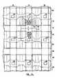
- an array of such devicesis illustrated which can provide such a density.
- the memory cell arrayis enclosed in dotted line 82, while a single cell of the memory array is enclosed in dotted line 84.
- the peripheral circuitry on the deviceincludes conventional row address decoding circuitry 86, column address decoding circuitry 88, sense amplifier circuitry 90, output buffer circuitry 92, and input buffer circuitry 94. These conventional circuits correspond to the peripheral devices discussed earlier in the fabrication section.
- Figure 5aillustrates a typical prior art EEPROM memory cell, such as enclosed by dotted line 96. Due to the programming and erase voltage requirements for previous EEPROM devices, a select transistor 98 is required in conjunction with the EEPROM transistor 100. The select transistor serves to isolate EEPROM transistors from the other memory cells when a particular memory cell is being operated upon. As such, a typical E EP ROM memory cell of previous configurations require two transistors and approximately 165 square microns of surface area.
- a memory cell in accordance with the present inventionrequires only 25 square microns of area, and no select transistor.
- the array structure shown in Figure 5bcan be utilized.
- cell 84has its source connected to the source of transistor 102 in the next column.
- the drain of transistor 84is connected to the drain of transistor 104 in the same column.
- the junction of the drains for transistor 104 and for transistor 84are connected to a line 106 from column address decode circuitry 88.
- Line 106is connected to all other drain junctions of the transistors in the column shared by transistors 84 and 104.
- the gate of transistor 84is connected to line 108 from row address decode circuitry 86.
- Line 108is connected to the gates of all transistors in the same row as transistors 84 and 102.
- a common connection for these source lines to each of the memory cellsis shown. Due to the interconnect configuration of the array 82 a common source connection can be used yet programming individual cells and erasing of all the cells can be obtained. For example, if cell 84 is desired to be programmed, line 106 from column address decode circuitry 88 is raised to high voltage as is line 108 from row address decode circuitry 86. At the same time common source line 110 is held at a ground potential. Because the drain lines on all of the other cells in the other columns are grounded, and because the gate lines for all of the other cells in the same row, as cell 84, are grounded, the contents of the other memory cells will not be effected.
- the common line 110is raised to the high potential level and the corresponding gate line, 108, is held at a ground potential.
- the common line 110is raised to the high potential level and the corresponding gate line, 108, is held at a ground potential.
- isolating transistorscan be added at selected intervals among the columns.
- a byte erase scheme in the arrayis achieved by adding an extra select transistor per byte of cells. This is shown in Figure 5d.
- Byte 1In order to erase Byte 1, the WL2 line is brought high and the source line, e.g. 126, for the corresponding byte is brought high. All the other wordlines are held low. All bit lines (column), e.g. 128, are kept floating. Under these conditions, cells in Byte 1 see a high voltage on the source and low voltage on the gate. This causes the cells to erase to a low V condition. Byte 2 is not disturbed because both gate and source are high and the drain is floating.
- all of the unselected source linesare held at an intermediate level, e.g. 5 volts.
- the asymmetrical structure of the source/drain junction itself and the programming configuration of the present inventionprovide a measure of protection from inadvertent modification of unselected bytes served by the WL2 line, even without raising the unselected source lines to the intermediate level.
- the channel 58is conductive.
- the capacitance seen by the floating gateis equivalent to the capacitance across the entire channel, e.g. capacitors 72, 74 and 76 in Figure 4.
- the Fowler-Nordheim tunneling effectwill be inoperative and no change in the charge on the floating gate will occur.
- the channel 58is non conductive. Only the overlap region 62 is conductive.
- the floating gatesees a much smaller capacitance, e.g. only capacitor 76 in Figure 4, and the coupling ratio is accordingly much higher, e.g. 0.8 to 0.9. With a higher coupling ratio, Fowler-Nordheim tunneling will occur.
- the capacity to erase a column of bytescan be obtained by modification of the structure in Figure 5b. To do so, a separate source line can be provided for each column of bytes. Thus, in Figure 5b this is shown implemented by opening the row address line, or word line, at points 130, and adding separate source lines (dashed lines 132) as indicated. In this configuration, an entire column of bytes can be selected for erasure.
- Dotted lines 112 and 114each indicate a single memory cell.
- Regions'116indicated by parallel lines, represent a metalization layer which extends vertically, in the figure, across each of the cells to interconnect the drain junctions of the cells.
- Regions 118defined by dotted/dashed lines, define the boundary between the field isolation oxide and the active/diffusion area.
- Regions 120defined by a straight line and a periodically varying line, define the control gate layer which extends across the memory cells of a common row.
- the shaded region 122represents the layers of the control gate, the second layer of dielectric material 66, the floating gate 64, and the gate dielectric 60.
- the drain connection for each memory cellcan be seen as represented by rectangles 124. It is to be noted that regions 124 interconnect the drains of adjacent memory cells in each column. In the manner above, a compact, high density EEPROM memory array can be obtained.
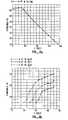
- Figure 6aillustrates the experimental results for programming and erasing of the EEPROM cell of the present invention.
- Figure 6aillustrates the erasing characteristics of the present invention.
- the vertical axisrepresents the threshold voltage for the cell, while the horizontal axis represents the magnitude of the pulse applied to the source terminal of the cell.
- threshold voltages on the order of 0 to 1 voltcan be obtained for pulse amplitudes of approximately 12 volts.
- the vertical axisrepresents the threshold voltage for the cell, while the horizontal axis represents the drain voltage.
- the curve comprising closely-spaced dotsrepresents a pulse amplitude on the gate of 12 volts, while the curve of widely-spaced dots represents a gate pulse amplitude of 11 volts.
- the solid line curverepresents a gate pulse amplitude of 10 volts.
- drain voltages on the order of 5 to 7 voltswill produce threshold levels in excess of 3 volts when a gate pulse between 10 and 12 volts is used.
Landscapes
- Engineering & Computer Science (AREA)
- Microelectronics & Electronic Packaging (AREA)
- Physics & Mathematics (AREA)
- Condensed Matter Physics & Semiconductors (AREA)
- General Physics & Mathematics (AREA)
- Manufacturing & Machinery (AREA)
- Computer Hardware Design (AREA)
- Power Engineering (AREA)
- Non-Volatile Memory (AREA)
- Semiconductor Memories (AREA)
- Read Only Memory (AREA)
- Electronic Switches (AREA)
- Insulated Gate Type Field-Effect Transistor (AREA)
- Networks Using Active Elements (AREA)
- Techniques For Improving Reliability Of Storages (AREA)
- Static Random-Access Memory (AREA)
- Bipolar Transistors (AREA)
- Design And Manufacture Of Integrated Circuits (AREA)
Abstract
Description
- The present invention is directed to an electrically programmable and erasable device and a method for making the same. The electrically programmable memory device can be of the type that is commonly called Electrically Erasable Programmable Read Only Memory (EEPROM). More particularly, the present invention relates to the structure and manufacture of a single transistor EEPROM cell suitable for use in high density memory devices.
- EEPROM devices and methods for making such devices are well known in the art. In general, an EPROM or an EEPROM is characterized by a "floating gate" and an electrical connection termed a "control gate", both of which are fabricated out of polycrystalline silicon doped with an appropriate doping material to render the polycrystalline conductive. A typical doping material is phosphorus.
- The floating gate is separated from a substrate region by a gate oxide layer of insulating material. The substrate region includes symmetrical source and drain regions which define a channel.
- The floating gate and the control gate are separated by a layer of insulating material, typically silicon dioxide (Si02). The principle upon which the EPROM or EEPROM device operates is that electrons, or charge, are stored on the "floating gate" in a capacitive manner. Thus, the dielectric layer between the floating gate and the control gate is important.
- In the prior art (see for example, U.S. Patent No. 4,203,158 and W.S. Johnson et al. ISCCC Digest of Technical Papers, pp. 152-153 (Feb., 1980)), the floating gate is formed by reacting SiH4 in a low pressure chemical vapor deposition chamber and then doped with POC13 in a separate doping cycle.
- A layer of silicon dioxide is then deposited or thermally grown on the doped polycrystalline layer of silicon. The layer of silicon dioxide is typically approximately 750 angstroms. Generally, a high oxidation temperature (greater than 1050 degrees C) and heavier phosphorus doping are required to achieve better interpoly quality and breakdown capability. However, oxidation at high temperature on heavily-doped polysilicon involves several drawbacks, such as: (1) outgassing during interpoly oxidation which causes autodoping on the wafer; and (2) oxidation enhanced diffusion of phosphorus from the floating gate to the tunnel oxide, which forms trapping centers in the oxide. The electron trapping collapses the threshold window EEPROM cell at 104 cycles. (See: R.B. Marcus et al., J. Electrochem. Soc., p. 1282, June, 1982; K. Saraswat et al., Computer-Aided Design of Integrated Circuit Fabrication Process for VLSI Device, p. 244-290, July, 1981.) Thus, current devices exhibit low cyclability for program and erase operations.
- Finally, the second layer of doped polycrystalline silicon is formed on top of the insulating layer of
S i02. - Because the insulating layer of silicon dioxide is on the order of 750 angstroms, the typical write or erase voltage, i.e., the voltage which is needed to place charge on or to remove charge from the floating gate, has been high, i.e., in excess of 20 volts. In turn, this places shrinkage limits on gate oxide thickness, junction depth and die size.
- Silicon nitride (Si3N4) has also been used as an insulating layer of dual dielectric (thermal oxide with silicon nitride on it) between the floating gate and the control gate connection. Silicon nitride has the property that it is more dense than silicon dioxide and, therefore, affords higher capacitive coupling between the floating gate and the control gate. A typical dual dielectric between the floating gate and the control gate is composed of 500 angstroms oxide and 400 angstroms nitride. However, even with the use of silicon nitride as the insulting layer, the write and erase voltage is still relatively high, in excess of 18 volts. High erase and program voltages for conventional EEPROM devices are of major concern. Such a requirement has led to the need for a separate high voltage supply when operating the devices, or for the use of special voltage multiplying circuitry within the device for boosting the supply voltage to the requisite program and erase levels.
- An additional drawback is that current EEPROM structures, when used in a memory array, require additional control circuitry to isolate individual storage cells from one another. This increases the device geometry. For example, given the requirement of a control transistor for each EEPROM cell, the equivalent space requirement for a conventional EEPROM cell is 165 square microns.
- These and other problems of previous EEPROM devices are overcome by the present invention of an electrically erasable programmable memory device comprising a body of single crystalline semiconductive material having a source and a drain, a first layer of insulating material positioned on the body, a floating gate positioned on the first layer of insulating material, a second layer of insulating material positioned on the floating gate, and a gate over the second layer of insulating material, wherein the source is formed of a deep region of a first material, such as phosphorous and a shallower region of a second material, such as arsenic and phosphorous, and the drain is formed of a shallow region of the second material, and further wherein a portion of a part of the deep region, such as arsenic only, underlies the first layer of insulating material and the first material is selected to optimize the junction overlap with the gate, in order to control capacitive coupling between the floating gate and the source.
- In another aspect of the present invention, the first layer of insulating material is thinner with respect to the second layer, and the first layer of insulating material is substantially free from traps.
- In another feature of the present invention the second layer of insulating material is chosen to have a high dielectric constant. Such a requirement can be satisfied by a sandwich of oxide-rich tantalum pentoxide and thermal oxide.
- With the above described structure an EEPROM cell is provided which is programmable as if it were an EPROM and erasable like an EEPROM. In order to program the device, the drain and gate of the device are raised to predetermined potentials above the potential of the source. To discharge or erase the cell the drain is floated and the source is raised to a potential above that of the gate.
- Because of the above discussed programming and erasing characteristics of the device of the present invention, a memory cell can be formed of a single such device without the need for a select transistor. Further, because of the selection of the first and second layers of insulating material and the asymmetrical shape of the source/drain region, a significantly smaller cell size can be provided along with a lower programming voltage requirement.
- Further, it has been found that growing a layer of tantalum pentoxide on a thermal oxide layer by reactive sputtering, and by using argon and oxygen as the sputtering gas, provides a high quality tantalum pentoxide layer for the second layer of insulating material.
- Further it has been found that by growing oxynitride as the first layer of insulating material at 850 degrees C in dry oxygen, and then annealing the material at 1050 degrees C in an ammonia/argon ambient, a layer which is substantially free of traps is provided.
- Additionally, it has been found that by in situ doping the floating gate one can obtain an exceptionally smooth surface upon which to grow the second layer of insulating material.
- It is therefore an object of the present invention to provide an EEPROM transistor which itself can be used as a complete memory cell.
- It is another object of the present invention to provide a memory device which is programmable in the manner of an EPROM device and erasable in the manner of an EEPROM device.
- It is a further object of the present invention to provide an EEPROM transistor having a small surface area.
- It is still another object of the present invention to provide an EEPROM cell which requires substantially lower programming and erasing voltages as compared to that of the prior art.
- These and other objectives, features and advantages of the present invention will be more readily understood upon consideration of the following detailed description of the preferred embodiment of the present invention and the accompanying drawings.
- Figure 1 is a cross section of a conventional EPROM device.
- Figure 2 is an illustration of a conventional EEPROM device.
- Figure 3a is a top view of the present invention.
- Figure 3b is a cross sectional view of the present invention taken along
lines 3b-3b of Figure 3a. - Figure 3c is a cross sectional view of the present invention taken along
line 3c-3c of Figure 3a. - Figure 4 illustrates the equivalent capacitive circuit of the device of the present invention.
- Figure 5a is a simplified schematic diagram of conventional EEPROM cells connected in a memory array.
- Figure 5b is a simplified schematic of EEPROM transistors of the present invention connected in a memory array with a block erase feature.
- Figure 5c is a top view of the geometry of an array of memory cells constructed according to the present invention.
- Figure 5d is a simplified schematic of EEPROM transistors of the present invention connected in a memory array with'a byte erase feature.
- Figure 6a illustrates the erasing conditions and characteristics of the device of the present invention.
- Figure 6b illustrates a typical programming characteristics and conditions of a device constructed in accordance with the present invention.
- Referring now to Figure 1 a cross section of a typical EPROM transistor device is shown. A
source 10 and adrain 12 are formed on asubstrate 14. Thesource 10 and drain 12 define achannel 16 in thesubstrate 14. Positioned above thechannel 16 is a layer of insulating material which forms agate dielectric layer 18. A floatinggate 20 of semiconductive material is formed over thegate dielectric layer 18. Asecond layer 22 of insulatingmaterial 22 is formed over the floatinggate 20. Finally, a layer of semiconductive material is formed over the second layer of insulatingmaterial 22 to form acontrol gate 24. Afield oxide 26 isolates the transistor structure from periphery devices. Electrical connections drain 12,gate 24, andsource 10, respectively.- Programming of the typical EPROM cell is accomplished by raising the potential of the
drain 12 to between 8 and 12 volts, holding thesource 10 at ground potential, and applying a pulse of approximately 13 to 21 volts amplitude to thecontrol gate 24, and having a period of approximately 1 to 10 milliseconds. - The result of these conditions is that a conductive region is established in the
channel 16 across whichelectrons 32 are accelerated. This conductive region is designated by the dashedline 34 of Figure 1. The magnitude and polarity of the voltages applied to thedrain 12,source 10 andgate 24 are such that thisconductive region 34 is "pinched off" in a region adjacent to drain 12. This causes theelectrons 32 to be raised sufficiently in potential so that they become "hot", these hot electrons create additional electron- hole pairs by impact ionization. In this condition these electrons are elevated to an energy level which permits them to overcome the insulating property ofgate dielectric 18. The hot electrons can thus "jump" the potential barrier of thegate dielectric 18. Thereafter, due to the electric field created by thecontrol gate 24,they are attracted to floatinggate 20 where they are stored. - The significant disadvantage of the EPROM structure is the requirement that the EPROM be erased by exposure to ultraviolet light. When the EPROM cells are in an array, effectively all such cells are erased together. Thus, when changes are sought to be made to a program stored in the array, even when the changes are minor, the entire array must be erased and the entire program rewritten into the array.
- Referring to Figure 2, there is shown an EEPROM structure. This structure utilizes a different mechanism for programming and erasing as compared to the EPROM structure. As with the EPROM structure, the EEPROM structure has a
drain 36, asource 38, a floatinggate 32 separated from the substrate by agate oxide layer 43, agate 40 separated from the floatinggate 32 by anotheroxide layer 45, all of which are deposited or thermally grown. However, the EEPROM structure differs from the EPROM structure in that it provides athin tunnel dielectric 46 between thedrain 36 and the floatinggate 42. As can be seen from Figure 2, the portion of the floatinggate 42 which is positioned above thetunnel dielectric 46 is positioned on thedrain 36. 'Further, the portion ofgate 40 which is aligned with thetunnel dielectric 46 is also positioned on the drain.36. Programming and erasing of this structure is achieved by inducing potential differences between the gate and drain lines, 48 and 50, respectively, which are on the order of 20 volts. The thin dielectric region coupled with the high voltage between gate and drain permits a phenomenon called "Fowler-Nordheim tunneling". To program, i.e. to place electrons on the floating gate, the drain is held at a ground potential while the gate is pulsed for approximately 10 milliseconds at a potential of approximately 20 volts. To erase, i.e. to remove electrons from the floatinggate 42, the gate is held at a ground potential while thedrain 36 is pulsed for approximately 10 milliseconds at a potential of approximately 20 volts. During the erase and program operations, thesource 38 is permitted to float. Under these conditions electrons can tunnel through the tunnel dielectric 46 to or from floatinggate 42. - With the above EEPROM structure an individual EEPROM cell can be selectively programmed or erased. Typically, all cells in an array are programmed to the same logic value, and thereafter individual cells are selectively erased, in order to place the final logical values in the array. However, as discussed earlier, among the disadvantages of the typical EEPROM structure are: 1) the requirement of a high voltage to program or erase the cell, and 2) the requirement of a select transistor for each EEPROM cell for isolating each cell when the EEPROM cells are used in an array.
- Referring now to Figures 3a, 3b, and 3c, the structure of the present invention will now be described. The structure of the present invention features an asymmetrical drain/source junction, a uniformly thin gate dielectric, and a dielectric between the control gate and the floating gate which has a high dielectric constant. As a result of these features, an EEPROM device is obtained which is programmed in a manner similar to an EPROM, and is erased in a manner similar to an EEPROM, but at a lower voltage, all with same physical size as an EPROM, and without requirement for select transistors when used in an array.
- Figure 3b illustrates a cross sectional view of the preferred embodiment of the present invention. A
substrate 52 has formed in it a relativelyshallow drain region 54, and adeeper source region 56. Achannel 58 is defined between thesource 56 anddrain 54. Agate dielectric 60 is formed over thechannel 58 and to extend betweendrain 54 and to overlap aportion 62 ofsource 56. It is to be noted that this layer has a relatively uniform thickness over the entire cross section. - A floating
gate 64 is formed over thegate dielectric 60. A second layer ofdielectric material 66 is formed over the floatinggate 64. Finally acontrol gate 68 is formed over the second layer of insulatingmaterial 66. - Figure 3a shows a top view of the physical positioning of the various component parts of the present invention. As can be seen from the figure the
control gate 68 and floatinggate 64 are positioned above one another and thechannel 58. Thesource diffusion 56 extends under the floatinggate 64. Figure 3c is a cross sectional view of the present invention taken alonglines 3c-3c of Figure 3a. As can be seen from Figures 3b and 3c, the structure of the present invention is noticeably more symmetrical than that of the typical EEPROM, yet more asymmetrical than than of the typical EPROM structures. More specifically, the device of the present invention lacks the pronounced "dip" in the gate dielectric, floating gate, intergate dielectric, and control gate associated with the tunneling dielectric of conventional EEPROMs. Further, the asymmetrical source/drain configuration of the present invention is noticeably different from the symmetrical source/drain junctions of conventional EPROMs. - In operation, programming of the EEPROM cell of the present invention is achieved by raising the
drain 54 andcontrol gate 68 to predetermined potentials above that of thesource 56. In the preferred embodiment of the present invention thedrain 54 is raised to between 4 and 6 volts, while the gate is pulsed at an amplitude of approximately 10 to 12 volts for approximately 0.5 to 5 msec. Under these conditions "hot" electrons are generated and accelerated across thegate dielectric 60 and onto the floatinggate 64. In the preferred embodiment of the present invention, this results in an increase of the floating gate threshold by approximately 3.5 to 5.5 volts. Thus, the programming operation in the present invention is similar to that of a typical EPROM. - On the other hand, erasing of the EEPROM cell of the present invention is achieved by floating the
drain node 54, holding thecontrol gate 68 at ground potential, and applying a pulse of high voltage to thesource 56. In the preferred embodiment of the present invention this pulse has an amplitude between 10 and 13 volts and a duration of between 0.5 and 5 msec. Under these conditions, Fowler-Nordheim tunneling occurs between the floatinggate 64 and theportion 62 of thesource diffusion 56 which underlies the floatinggate 64. The erasing operation causes the threshold voltage of the cell to be reduced to a level on the order of one volt. - The above mix of programming and erase mechanisms, in part, alleviate the requirement of a separate select transistor for each memory cell in an array of memory cells of the present invention.
- The logical condition of the cell is determined in a manner similar to that in connection with an EPROM cell. The
source 56 is held at a ground potential, the gate is held at a potential between three to five volts, and the drain is held at a potential between one to two volts. Under these conditions, an erased cell will conduct at a current level of between 25 to 50 microamps. On the other hand, a programmed cell will not conduct. - From the above it is to be appreciated that the improved performance of the present invention has been achieved not only by employing an EPROM programming mechanism, and an EEPROM erase mechanism, but also by providing an asymmetric source/drain junction, a
thin gate dielectric 60 having superior trapping characteristics, and a dielectric layer between thecontrol gate 68 and floatinggate 64 which has a high dielectric constant. It is to be understood that while each of the features, in and of themselves, contribute to improve to the performance of the present invention, the combination of these features results in an even greater improvement over previous EEPROM structures. - Referring to Figure 4, an equivalent circuit is illustrated which describes the capacitive coupling between the control gate, floating gate, source, channel, and drain. This capacitive coupling plays a substantial role in determining the amount of charge which is caused to be stored, or drawn from, the floating
gate 64 during a program, or erase, operation. The capacitive coupling between thecontrol gate 68 and the floatinggate 64 is shown represented bycapacitor 70. The capacitive coupling between the floatinggate 64 and drain 54 is represented by capacitor 72. The capacitive coupling between the floatinggate 64 andchannel 58 is represented bycapacitor 74. Finally, the capacitive coupling between the floatinggate 64 and thesource 56 is represented bycapacitor 76. - It can be shown that the voltage, VFG, across the floating
gate 64 with respect to thesubstrate 52, is defined by the equation
where the voltage VG is applied to the control gate. - The higher the voltage across the floating
gate 64, the larger the amount of electrons stored on the floating gate. In turn, the more electrons on the floating gate, the higher the threshold of the device. - The structure of the present invention maximizes the voltage across the floating gate in a number of ways. With respect to the dielectric 66, it has been found that by selecting a material having a high dielectric constant, i.e., greater than 5, the voltage coupled to the floating gate can be increased. In the preferred embodiment to the present invention tantalum pentoxide can be used. Tantalum pentoxide has a dielectric constant of approximately 21. Silicon nitride, which has a dielectric constant of 7, can also be used. This'permits a high capacitance value with small physical size. The larger the value of
capacitor 70, the smaller the impact ofcapacitors gate 64. A typical cell size for the present invention is 5 microns by 5 microns and can be reduced further with improved lithography techniques. - It has been found that the retention characteristics of the tantalum pentoxide can be increased when the dielectric layer of 66 is formed of a sandwich of tantalum pentoxide and of thermal oxide. Preferably, the tantalum pentoxide layer is approximately 500 angstroms thick, while the thermal oxide layer is approximately 150 angstroms thick. Further, it has been found that a slightly oxide-rich tantalum pentoxide material yields improved data retention. The layer of thermal oxide has been found to permit the use of higher temperature cycles in the fabrication process than would normally be permissible when tantalum pentoxide is used alone. Further, the thermal oxide layer reduces the leakage current through tantalum pentoxide.
- The selection of the
gate dielectric 60 is another means by which the performance of the device is enhanced. As can be seen from Figure 3b, thecapacitance 76 in the Figure 4 between the floatinggate 64 and thesource 56 is a function of theoverlap area 62 between thegate dielectric 60 and thesource 56, the gate dielectric constant, and the thickness of the gate dielectric. In the preferred embodiment of the present invention thegate dielectric 60 has a thickness in the 100 to 200 angstrom range. Preferably, the gate dielectric is formed from oxynitride, and theoverlap region 62 is kept small, preferably 0.3 to 0.4 micrometers. - There are a number of factors which influence the selection of these parameters. One such factor is the cyclability of the cell between a programmed and erased condition. This cyclability is determined, in part, by the trapping characteristics of the
gate dielectric 60 and the current density flowing through thegate dielectric 60. The higher the current density, the lower the cyclability. Oxynitride is the preferred material for thegate dielectric layer 60 in that, in accordance with the method of the present invention, it can be made relatively free from trapping effects. It has also been found that oxynitride is a good barrier with respect to phosphorous migration,thus, preserving the integrity of the floatinggate 64. - Current density in the
gate dielectric layer 60 is a function of the area and thickness dimensions of thelayer 60. The capacitance between the floatinggate 64 and thesource 56 is proportional to the thickness of thegate dielectric layer 60, and the current density through thegate dielectric layer 60 varies inversely with the thickness. The value ofcapacitance 76 is proportional to theoverlap portion 62 ofsource 56. - The thickness of the
gate dielectric layer 60 and the overlap ofportion 62 are thus chosen to optimize the current density through thelayer 60 and to optimize the capacitive coupling betweensource 56 and floatinggate 64. A further limitation to the thickness of the gate dielectric layer is that the Fowler-Nordheim tunneling effects require a thin dielectric layer. Thus, in the preferred embodiment of the present invention, the gate dielectric is preferably formed of oxynitride and has a thickness from between 100 and 200 angstroms. Further, theoverlap region 62 ofsource 56 is approximately 0.3 to 0.4 microns. With the above structure, cyclability in the order of 106 can be obtained. - As was discussed briefly above, the present invention also'includes an asymmetrical source/drain junction. In the preferred embodiment of the present invention the
source 56 is formed of ashallow diffusion region 78 and adeeper diffusion region 80. Thedeeper diffusion region 80 underlies the floating gate by approximately 0.2 microns, while theshallow diffusion region 78 underlies the floating gate by approximately 0.1 microns, to form the 0.3 to 0.4micron overlap region 62. In the preferred embodiment of the present invention thedrain diffusion 54 is formed from arsenic and underlies the floating gate by approximately 0.1 microns, theshallow source diffusion 78 is formed from arsenic and phosphorous, and thedeep diffusion portion 80 is formed from phosphorous. - A deep diffusion of phosphorous is utilized in the preferred embodiment of the present invention because its fast-diffusion property permits the formation of the
requisite overlap portion 62 while also providing a smoother curvature of thedeep diffusion portion 80. This smoother curvature greatly increases the breakdown voltage of the source junction. This is particularly important at thesource 56 because of the thinness of thegate dielectric 60 and the high voltages that the source sees during the erasing operations of the present invention. - In accordance with the method of the present invention the preferred embodiment of the cell of the present invention is compatible with CMOS processing. The starting material is p-type having a 100 orientation and a resistivity of 36 to 63 ohms- centimeter. This represents the p-
substrate 52 in Figure 3b. P 31 material is implanted in the N-wells at 90KeV with a density of 4.0 x 10¹²/cm2. The implant is driven into the wells by way of a wet oxidation for 45 minutes at 950 degrees centigrade, followed by a nitrogen, N2, drive at 1150 degrees centigrade. - Thereafter a pad oxide of 500 angstroms thickness is formed at 1000 degrees centigrade in an 02 atmosphere. Silicon nitride is thereafter deposited. The active area is then defined and a screen oxidation of 150 angstroms thickness is formed. The field area is then defined and the field is implanted with BF2 at 50KeV and a dose of4 x 10 /cm .
- Field oxide is then formed at 1000 degrees centigrade for 40 minutes in an atmosphere of 02, followed by 85 minutes at 920 degrees C in an atmosphere of N2. Followed by six hours at 920°c in H2/O2 to obtain a thickness of 6500 angstroms. The cell area is then defined and thereafter implanted with boron at 40KeV and dose 5 x 10 /cm . The preceding fabrication processes are conventional.
- Up to this point the drain and source areas have been defined, although not yet formed, and the channel portion has also been defined to thereby identify the active area of the cell. In the next step a cell oxide layer between 100 angstroms and 200 angstroms thick is grown at 850 degrees centigrade. This cell oxide layer represents the
gate dielectric 60. In order to provide a layer which is relatively free from trapping effects, the oxide is grown in a dry oxygen atmosphere. Thereafter thermal nitridation is performed on the oxide layer for 10 minutes at 1050 degrees centigrade in an atmosphere of ammonia (NH3) and argon (Ar). The high temperature, i.e., 1050 degrees centigrade, removes water, H20, from the layer, while the ammonia/argon atmosphere anneals any OH radicals from the material. The result is a relatively trap-free layer of oxynitride. - In the next step the floating
gate 64 is deposited over thegate dielectric 60. This involves in situ doping of polysilicon when the polysilicon is deposited as the floating gate. To do this, SiH4 and PH3 are combined by way of chemical vapor deposition to form Si (phosphorous-doped). By in situ doping of the polysilicon material additional high temperature fabrication steps can be avoided. This is important in order to minimize the grain size in the polysilicon. It has been found that with a smaller grain size of polysilicon, a smoother polysilicon surface is obtained thus permitting reliable thinner layers of oxide to be grown on the polysilicon surface. - The next step'involves the forming of the
dielectric layer 66 between thecontrol gate 68 and the floatinggate 64. In the preferred embodiment of the present invention this dielectric layer comprises a thin layer of thermal oxide and a relatively thick layer of tantalum pentoxide. The thermal oxide layer is grown first at a temperature of 1040 degrees centigrade. This is followed by the step of sputtering ultra pure tantalum using an argon/oxygen sputtering gas. In the preferred embodiment of the present invention the argon to oxygen ratio is approximately 4:1. Preferably the oxygen content of the sputtering gas is at least 25%. Also, it is preferred that the resulting tantalum pentoxide deposition Ta205 is slightly oxide rich so that the composition is approximately Ta205.25 to Ta205.5' As a result of this tantalum pentoxide/silicon dioxide sandwich, leakage current between thecontrol gate 68 and floatinggate 64 is reduced, and the coupling ratio enhanced. The amount of voltage between the floating gate and substrate during an erase or program operation, is thus increased. - Thereafter, the tantalum pentoxide, thermal oxide, and
polysilicon layers 20, are subjected to an etch to define the floatinggate 64 in the direction shown in Figure 3c. - In the typical fabrication process of the cells of the present invention peripheral circuitry, such as sense transistors, address decoding circuitry and the like, are also provided on the same chip. Thus, where such other peripheral devices are present, the next step is to form these devices. It is to be understood, however, that where peripheral devices are not present the next step in the fabrication process would be the deposition of the control gate layer.
- Under the former circumstances, where peripheral devices are being formed on the same chip, the gate dielectric for these peripheral devices are formed to a thickness of approximately 300 angstroms and at a temperature of approximately 1000 degrees C. Thereafter a two-step boron implant is performed on the oxide layer. This creates a slightly deeper concentration of boron to reduce the occurrence of source/drain punch-through problems. The first boron implant is conducted at 50KeV while the second is conducted at 100KeV to form a "two-bump" implant profile.
- Thereafter, the
control gate layer 68 is formed, preferably of polysilicon. This layer represents the conventional control gate for the peripheral devices. This layer is then doped in a conventional manner. - The above steps are then followed by the definition and etching of the control gate areas.
- Thereafter, the source and drain areas are masked and implanted with arsenic to a depth of approximately 0.2 to 0.3 micrometers. Then the drain areas are masked off and a high voltage implant is performed with phosphorous into the source areas of the EEPROM cells. It has been found that the fast diffusion characteristics of phosphorous provides the mechanism by which the
overlap portion 62 between floatinggate 64 and thesource 56 can be obtained, as well as the smooth curvature required for high breakdown voltage in the source junction. - The above steps are then followed by implantation of source and drain regions for the p-channel peripheral devices. Thereafter a BPSG deposition is conducted at 390 degrees centigrade and a thickness of 1 micron, followed by a densification of the glass at 900 degrees centigrade for 20 minutes in a steam oxidation atmosphere. Finally, N + plug implants are performed using phosphorous at 50KeV and a dose of 3 x10¹⁵/cm2, to reduce spiking problems in the contact area.
- The above steps are followed by conventional damage removal, metalization, and passivation.
- The device structure and method discussed above permits the formation of high density EEPROM memories, for example, of one megabit density. Referring to Figure 5b, an array of such devices is illustrated which can provide such a density. The memory cell array is enclosed in
dotted line 82, while a single cell of the memory array is enclosed indotted line 84. The peripheral circuitry on the device includes conventional rowaddress decoding circuitry 86, columnaddress decoding circuitry 88,sense amplifier circuitry 90,output buffer circuitry 92, andinput buffer circuitry 94. These conventional circuits correspond to the peripheral devices discussed earlier in the fabrication section. - Figure 5a illustrates a typical prior art EEPROM memory cell, such as enclosed by
dotted line 96. Due to the programming and erase voltage requirements for previous EEPROM devices, aselect transistor 98 is required in conjunction with theEEPROM transistor 100. The select transistor serves to isolate EEPROM transistors from the other memory cells when a particular memory cell is being operated upon. As such, a typical EEPROM memory cell of previous configurations require two transistors and approximately 165 square microns of surface area. - In contrast, because of the programming and erase requirements for the EEPROM cell of the present invention, a memory cell in accordance with the present invention requires only 25 square microns of area, and no select transistor. Thus, the array structure shown in Figure 5b can be utilized.
- There it can be seen that adjacent transistors are reversed in orientation. Thus, in the upper left-hand corner of the array,
cell 84 has its source connected to the source oftransistor 102 in the next column. The drain oftransistor 84 is connected to the drain oftransistor 104 in the same column. The junction of the drains fortransistor 104 and fortransistor 84 are connected to aline 106 from columnaddress decode circuitry 88.Line 106 is connected to all other drain junctions of the transistors in the column shared bytransistors transistor 84 is connected to line 108 from rowaddress decode circuitry 86. Line 108 is connected to the gates of all transistors in the same row astransistors - A common connection for these source lines to each of the memory cells is shown. Due to the interconnect configuration of the array 82 a common source connection can be used yet programming individual cells and erasing of all the cells can be obtained. For example, if
cell 84 is desired to be programmed,line 106 from columnaddress decode circuitry 88 is raised to high voltage as is line 108 from rowaddress decode circuitry 86. At the same time common source line 110 is held at a ground potential. Because the drain lines on all of the other cells in the other columns are grounded, and because the gate lines for all of the other cells in the same row, ascell 84, are grounded, the contents of the other memory cells will not be effected. - Similarly, in the event that an erase mode is desired, the common line 110 is raised to the high potential level and the corresponding gate line, 108, is held at a ground potential. As can be seen from Figure 5b, due to the common connection of the source terminals of the memory cells in each row, all cells in all of the rows will be erased. In the event that smaller segments of the row are desired to be selectively erasable at any one time, isolating transistors can be added at selected intervals among the columns.
- A byte erase scheme in the array is achieved by adding an extra select transistor per byte of cells. This is shown in Figure 5d.
- In order to erase
Byte 1, the WL2 line is brought high and the source line, e.g. 126, for the corresponding byte is brought high. All the other wordlines are held low. All bit lines (column), e.g. 128, are kept floating. Under these conditions, cells inByte 1 see a high voltage on the source and low voltage on the gate. This causes the cells to erase to a low V condition.Byte 2 is not disturbed because both gate and source are high and the drain is floating. - In the preferred embodiment of the present invention, in order to ensure that the data in the unselected bytes on WL2 remain undisturbed, all of the unselected source lines are held at an intermediate level, e.g. 5 volts. The asymmetrical structure of the source/drain junction itself and the programming configuration of the present invention provide a measure of protection from inadvertent modification of unselected bytes served by the WL2 line, even without raising the unselected source lines to the intermediate level.
- It is believed that the above is true for the following reasons. When the gate is high and the source is at a lower potential, as is the case with the bytes served by WL2, the
channel 58 is conductive. Thus, the capacitance seen by the floating gate is equivalent to the capacitance across the entire channel,e.g. capacitors Byte 1, thechannel 58 is non conductive. Only theoverlap region 62 is conductive. Thus, the floating gate sees a much smaller capacitance, e.g. only capacitor 76 in Figure 4, and the coupling ratio is accordingly much higher, e.g. 0.8 to 0.9. With a higher coupling ratio, Fowler-Nordheim tunneling will occur. - The capacity to erase a column of bytes can be obtained by modification of the structure in Figure 5b. To do so, a separate source line can be provided for each column of bytes. Thus, in Figure 5b this is shown implemented by opening the row address line, or word line, at
points 130, and adding separate source lines (dashed lines 132) as indicated. In this configuration, an entire column of bytes can be selected for erasure. - Referring to Figure 5c, the physical geometry of the
array structure 82 of Figure 5b is shown in part.Dotted lines 112 and 114 each indicate a single memory cell. Regions'116, indicated by parallel lines, represent a metalization layer which extends vertically, in the figure, across each of the cells to interconnect the drain junctions of the cells.Regions 118, defined by dotted/dashed lines, define the boundary between the field isolation oxide and the active/diffusion area.Regions 120, defined by a straight line and a periodically varying line, define the control gate layer which extends across the memory cells of a common row. Within a particular memory cell, for example 112, the shadedregion 122 represents the layers of the control gate, the second layer ofdielectric material 66, the floatinggate 64, and thegate dielectric 60. Finally, the drain connection for each memory cell can be seen as represented byrectangles 124. It is to be noted thatregions 124 interconnect the drains of adjacent memory cells in each column. In the manner above, a compact, high density EEPROM memory array can be obtained. - Finally, referring to Figures 6a and 6b, the experimental results for programming and erasing of the EEPROM cell of the present invention are illustrated. Figure 6a illustrates the erasing characteristics of the present invention. As can be seen from the figure, the vertical axis represents the threshold voltage for the cell, while the horizontal axis represents the magnitude of the pulse applied to the source terminal of the cell. Thus it can be seen that threshold voltages on the order of 0 to 1 volt can be obtained for pulse amplitudes of approximately 12 volts.
- Referring to Figure 6b, the programming characteristics of the cell are shown. The vertical axis represents the threshold voltage for the cell, while the horizontal axis represents the drain voltage. The curve comprising closely-spaced dots represents a pulse amplitude on the gate of 12 volts, while the curve of widely-spaced dots represents a gate pulse amplitude of 11 volts. Finally, the solid line curve represents a gate pulse amplitude of 10 volts. As can be seen from the figure, drain voltages on the order of 5 to 7 volts will produce threshold levels in excess of 3 volts when a gate pulse between 10 and 12 volts is used.
- Clearly, the programming and erase characteristics shown in these figures are far superior to that of presently available EEPROM memory cells.
- The terms and expressions which have been employed here are used as terms of description and not of limitations, and there is no intention, in the use of such terms and expressions of excluding equivalence of the features shown and described, or portions thereof, it being recognized that various modifications are possible within the scope of the invention claimed.

Claims (44)
Priority Applications (2)
| Application Number | Priority Date | Filing Date | Title |
|---|---|---|---|
| AT85114090TATE104473T1 (en) | 1984-11-21 | 1985-11-05 | ELECTRICALLY PROGRAMMABLE SINGLE TRANSISTOR DEVICE AND METHOD. |
| EP93102713AEP0550404B1 (en) | 1984-11-21 | 1985-11-05 | A method of making a capacitive coupling device, especially in an EEPROM |
Applications Claiming Priority (2)
| Application Number | Priority Date | Filing Date | Title |
|---|---|---|---|
| US06/673,946US4698787A (en) | 1984-11-21 | 1984-11-21 | Single transistor electrically programmable memory device and method |
| US673946 | 1984-11-21 |
Related Child Applications (3)
| Application Number | Title | Priority Date | Filing Date |
|---|---|---|---|
| EP93102713ADivisionEP0550404B1 (en) | 1984-11-21 | 1985-11-05 | A method of making a capacitive coupling device, especially in an EEPROM |
| EP93102713ADivision-IntoEP0550404B1 (en) | 1984-11-21 | 1985-11-05 | A method of making a capacitive coupling device, especially in an EEPROM |
| EP93102713.0Division-Into | 1985-11-05 |
Publications (3)
| Publication Number | Publication Date |
|---|---|
| EP0182198A2true EP0182198A2 (en) | 1986-05-28 |
| EP0182198A3 EP0182198A3 (en) | 1988-05-25 |
| EP0182198B1 EP0182198B1 (en) | 1994-04-13 |
Family
ID=24704721
Family Applications (2)
| Application Number | Title | Priority Date | Filing Date |
|---|---|---|---|
| EP93102713AExpired - LifetimeEP0550404B1 (en) | 1984-11-21 | 1985-11-05 | A method of making a capacitive coupling device, especially in an EEPROM |
| EP85114090AExpired - LifetimeEP0182198B1 (en) | 1984-11-21 | 1985-11-05 | Single transistor electrically programmable device and method |
Family Applications Before (1)
| Application Number | Title | Priority Date | Filing Date |
|---|---|---|---|
| EP93102713AExpired - LifetimeEP0550404B1 (en) | 1984-11-21 | 1985-11-05 | A method of making a capacitive coupling device, especially in an EEPROM |
Country Status (6)
| Country | Link |
|---|---|
| US (2) | US4698787A (en) |
| EP (2) | EP0550404B1 (en) |
| JP (3) | JPH0682841B2 (en) |
| AT (2) | ATE104473T1 (en) |
| CA (1) | CA1236919A (en) |
| DE (2) | DE3588238T2 (en) |
Cited By (23)
| Publication number | Priority date | Publication date | Assignee | Title |
|---|---|---|---|---|
| JPS6325981A (en)* | 1986-05-30 | 1988-02-03 | アトメル・コーポレイション | EEPROM that can be electrically erased |
| DE3833726A1 (en)* | 1987-10-21 | 1989-05-03 | Mitsubishi Electric Corp | SEMICONDUCTOR STORAGE DEVICE |
| FR2635408A1 (en)* | 1988-08-11 | 1990-02-16 | Sgs Thomson Microelectronics | HIGH INTEGRATION DENSITY EPROM MEMORY |
| FR2638285A1 (en)* | 1988-10-25 | 1990-04-27 | Commissariat Energie Atomique | HIGH-DENSITY INTEGRATED INTEGRATED CIRCUIT SUCH AS MEMORY EPROM AND CORRESPONDING OBTAINING METHOD |
| EP0305741A3 (en)* | 1987-07-31 | 1990-05-16 | Kabushiki Kaisha Toshiba | Semiconductor device with floating gate |
| FR2641128A1 (en)* | 1988-12-15 | 1990-06-29 | Samsung Electronics Co Ltd | Semiconductor electrically erasable and programmable memory device, and method for erasing and programming it |
| EP0370416A3 (en)* | 1988-11-23 | 1990-12-05 | National Semiconductor Corporation | Novel architecture for a flash erase eprom memory |
| FR2652189A1 (en)* | 1989-09-15 | 1991-03-22 | Intel Corp | BLOCK ERASURE "FLASH" EEPROM MEMORY. |
| EP0376290A3 (en)* | 1988-12-28 | 1991-07-03 | Kabushiki Kaisha Toshiba | Nonvolatile semiconductor memory device capable of preventing read error caused by overerase state |
| EP0503756A3 (en)* | 1991-03-13 | 1994-02-09 | Advanced Micro Devices Inc | |
| EP0495492A3 (en)* | 1991-01-17 | 1994-06-01 | Texas Instruments Inc | Non-volatile memory cell structure and process for forming same |
| US5341329A (en)* | 1988-12-28 | 1994-08-23 | Kabushiki Kaisha Toshiba | Nonvolatile semiconductor memory device capable of preventing read error caused by overerase state and method therefor |
| EP0637035A1 (en)* | 1993-07-29 | 1995-02-01 | STMicroelectronics S.r.l. | Circuit structure for a memory matrix and corresponding manufacturing method |
| EP0528564A3 (en)* | 1991-08-20 | 1995-03-08 | Nat Semiconductor Corp | |
| EP0655742A1 (en)* | 1993-11-30 | 1995-05-31 | STMicroelectronics S.r.l. | Integrated device with electrically programmable and erasable memory cells |
| EP0622806A3 (en)* | 1993-04-30 | 1995-10-18 | Toshiba Kk | Non-volatile semiconductor memory device. |
| EP0360504B1 (en)* | 1988-09-22 | 1996-04-10 | Advanced Micro Devices Inc. | One transistor flash eprom cell |
| EP0845785A1 (en)* | 1996-11-29 | 1998-06-03 | STMicroelectronics S.A. | Electronic non-volatile memory and its management method |
| EP0570597A4 (en)* | 1991-12-09 | 1998-11-11 | Fujitsu Ltd | Flash memory improved in erasing characteristic, and circuit therefor |
| EP1033754A1 (en)* | 1999-03-03 | 2000-09-06 | STMicroelectronics S.r.l. | Non-volatile semiconductor memory |
| EP1313148A3 (en)* | 1997-01-31 | 2004-03-03 | Integrated Memory Technologies, Inc. | A scalable flash eeprom memory cell, method of manufacturing and operation thereof |
| FR2970106A1 (en)* | 2010-12-29 | 2012-07-06 | St Microelectronics Sa | OTP MEMORY BASED ON MOSFET DEVICES |
| WO2014083511A1 (en) | 2012-11-27 | 2014-06-05 | I.P.S. Research And Development B.V. | Pressure control fill valve |
Families Citing this family (287)
| Publication number | Priority date | Publication date | Assignee | Title |
|---|---|---|---|---|
| US4939558A (en)* | 1985-09-27 | 1990-07-03 | Texas Instruments Incorporated | EEPROM memory cell and driving circuitry |
| US5189497A (en)* | 1986-05-26 | 1993-02-23 | Hitachi, Ltd. | Semiconductor memory device |
| JP2555027B2 (en)* | 1986-05-26 | 1996-11-20 | 株式会社日立製作所 | Semiconductor memory device |
| JP3059442B2 (en)* | 1988-11-09 | 2000-07-04 | 株式会社日立製作所 | Semiconductor storage device |
| KR910000139B1 (en)* | 1986-10-27 | 1991-01-21 | 가부시키가이샤 도시바 | Non-volatile semi-conductor memory device with double gate structure |
| JPS63179577A (en)* | 1987-01-21 | 1988-07-23 | Sony Corp | Nonvolatile memory |
| JPS63252481A (en)* | 1987-04-09 | 1988-10-19 | Toshiba Corp | non-volatile semiconductor memory |
| US5313420A (en)* | 1987-04-24 | 1994-05-17 | Kabushiki Kaisha Toshiba | Programmable semiconductor memory |
| JP2633252B2 (en)* | 1987-06-11 | 1997-07-23 | 沖電気工業株式会社 | Semiconductor storage device |
| US4920512A (en)* | 1987-06-30 | 1990-04-24 | Mitsubishi Denki Kabushiki Kaisha | Non-volatile semiconductor memory capable of readily erasing data |
| JP2602244B2 (en)* | 1987-09-24 | 1997-04-23 | 株式会社日立製作所 | Semiconductor storage device |
| US5016215A (en)* | 1987-09-30 | 1991-05-14 | Texas Instruments Incorporated | High speed EPROM with reverse polarity voltages applied to source and drain regions during reading and writing |
| US5194749A (en)* | 1987-11-30 | 1993-03-16 | Hitachi, Ltd. | Semiconductor integrated circuit device |
| US4861730A (en)* | 1988-01-25 | 1989-08-29 | Catalyst Semiconductor, Inc. | Process for making a high density split gate nonvolatile memory cell |
| US5304505A (en)* | 1989-03-22 | 1994-04-19 | Emanuel Hazani | Process for EEPROM cell structure and architecture with increased capacitance and with programming and erase terminals shared between several cells |
| US5677867A (en)* | 1991-06-12 | 1997-10-14 | Hazani; Emanuel | Memory with isolatable expandable bit lines |
| WO1989009494A1 (en)* | 1988-03-31 | 1989-10-05 | Solarex Corporation | Gate dielectric for a thin film field effect transistor |
| US5033023A (en)* | 1988-04-08 | 1991-07-16 | Catalyst Semiconductor, Inc. | High density EEPROM cell and process for making the cell |
| JP2799711B2 (en)* | 1988-05-10 | 1998-09-21 | 株式会社日立製作所 | Non-volatile storage element |
| US5153144A (en)* | 1988-05-10 | 1992-10-06 | Hitachi, Ltd. | Method of making tunnel EEPROM |
| US5445980A (en)* | 1988-05-10 | 1995-08-29 | Hitachi, Ltd. | Method of making a semiconductor memory device |
| US4949309A (en)* | 1988-05-11 | 1990-08-14 | Catalyst Semiconductor, Inc. | EEPROM utilizing single transistor per cell capable of both byte erase and flash erase |
| US5315547A (en)* | 1988-07-11 | 1994-05-24 | Hitachi, Ltd. | Nonvolatile semiconductor memory device with selective tow erasure |
| FR2635409B1 (en)* | 1988-08-11 | 1991-08-02 | Sgs Thomson Microelectronics | HIGH INTEGRATION DENSITY EPROM TYPE MEMORY HAVING HIGH COUPLING FACTOR, AND MANUFACTURING METHOD THEREOF |
| US5153684A (en)* | 1988-10-19 | 1992-10-06 | Kabushiki Kaisha Toshiba | Nonvolatile semiconductor memory device with offset transistor |
| US5095345A (en)* | 1988-11-10 | 1992-03-10 | Texas Instruments Incorporated | Floating-gate memory array with silicided buried bitlines |
| US5238855A (en)* | 1988-11-10 | 1993-08-24 | Texas Instruments Incorporated | Cross-point contact-free array with a high-density floating-gate structure |
| US5025494A (en)* | 1988-11-10 | 1991-06-18 | Texas Instruments Incorporated | Cross-point contact-free floating-gate memory array with silicided buried bitlines |
| US5023680A (en)* | 1988-11-10 | 1991-06-11 | Texas Instruments Incorporated | Floating-gate memory array with silicided buried bitlines and with single-step-defined floating gates |
| US5051796A (en)* | 1988-11-10 | 1991-09-24 | Texas Instruments Incorporated | Cross-point contact-free array with a high-density floating-gate structure |
| US5262846A (en)* | 1988-11-14 | 1993-11-16 | Texas Instruments Incorporated | Contact-free floating-gate memory array with silicided buried bitlines and with single-step-defined floating gates |
| IT1227989B (en)* | 1988-12-05 | 1991-05-20 | Sgs Thomson Microelectronics | EPROM MEMORY CELL MATRIX WITH TABLECLOTH STRUCTURE WITH IMPROVED CAPACITIVE RATIO AND PROCESS FOR ITS MANUFACTURE |
| US5296396A (en)* | 1988-12-05 | 1994-03-22 | Sgs-Thomson Microelectronics S.R.L. | Matrix of EPROM memory cells with a tablecloth structure having an improved capacitative ratio and a process for its manufacture |
| US5113238A (en)* | 1989-01-06 | 1992-05-12 | Wang Chen Chin | Contactless non-volatile memory array cells |
| US5844842A (en)* | 1989-02-06 | 1998-12-01 | Hitachi, Ltd. | Nonvolatile semiconductor memory device |
| US5196914A (en)* | 1989-03-15 | 1993-03-23 | Sgs-Thomson Microelectronics S.R.L. | Table cloth matrix of EPROM memory cells with an asymmetrical fin |
| US5081054A (en)* | 1989-04-03 | 1992-01-14 | Atmel Corporation | Fabrication process for programmable and erasable MOS memory device |
| US6373093B2 (en)* | 1989-04-28 | 2002-04-16 | Nippondenso Corporation | Semiconductor memory device and method of manufacturing the same |
| US5017979A (en)* | 1989-04-28 | 1991-05-21 | Nippondenso Co., Ltd. | EEPROM semiconductor memory device |
| JPH02295169A (en)* | 1989-05-09 | 1990-12-06 | Nec Corp | Nonvolatile semiconductor memory |
| GB2232798B (en)* | 1989-06-12 | 1994-02-23 | Intel Corp | Electrically programmable read-only memory |
| US5177705A (en)* | 1989-09-05 | 1993-01-05 | Texas Instruments Incorporated | Programming of an electrically-erasable, electrically-programmable, read-only memory array |
| JPH03102878A (en)* | 1989-09-18 | 1991-04-30 | Seiko Instr Inc | Electrically erasable nonvolatile semiconductor memory |
| JPH088314B2 (en)* | 1989-10-11 | 1996-01-29 | 株式会社東芝 | Nonvolatile semiconductor memory device and manufacturing method thereof |
| US5077691A (en)* | 1989-10-23 | 1991-12-31 | Advanced Micro Devices, Inc. | Flash EEPROM array with negative gate voltage erase operation |
| US5126808A (en)* | 1989-10-23 | 1992-06-30 | Advanced Micro Devices, Inc. | Flash EEPROM array with paged erase architecture |
| US5097444A (en)* | 1989-11-29 | 1992-03-17 | Rohm Corporation | Tunnel EEPROM with overerase protection |
| KR930000869B1 (en)* | 1989-11-30 | 1993-02-08 | 삼성전자 주식회사 | Page-Erasable Flash YPIROM Device |
| US5215934A (en)* | 1989-12-21 | 1993-06-01 | Tzeng Jyh Cherng J | Process for reducing program disturbance in eeprom arrays |
| IT1236601B (en)* | 1989-12-22 | 1993-03-18 | Sgs Thomson Microelectronics | INTEGRATED SEMICONDUCTOR DEVICE OF EPROM TYPE WITH METAL CONNECTIONS OF SOURCE AND PROCEDURE FOR ITS MANUFACTURE. |
| US5106772A (en)* | 1990-01-09 | 1992-04-21 | Intel Corporation | Method for improving the electrical erase characteristics of floating gate memory cells by immediately depositing a protective polysilicon layer following growth of the tunnel or gate oxide |
| US5067108A (en)* | 1990-01-22 | 1991-11-19 | Silicon Storage Technology, Inc. | Single transistor non-volatile electrically alterable semiconductor memory device with a re-crystallized floating gate |
| CA2051686C (en)* | 1990-01-22 | 2001-10-23 | Bing Yeh | Single transistor non-volatile electrically alterable semiconductor memory device with a re-crystallized floating gate |
| US5202850A (en)* | 1990-01-22 | 1993-04-13 | Silicon Storage Technology, Inc. | Single transistor non-volatile electrically alterable semiconductor memory device with a re-crystallized floating gate |
| US5242848A (en)* | 1990-01-22 | 1993-09-07 | Silicon Storage Technology, Inc. | Self-aligned method of making a split gate single transistor non-volatile electrically alterable semiconductor memory device |
| US5572054A (en)* | 1990-01-22 | 1996-11-05 | Silicon Storage Technology, Inc. | Method of operating a single transistor non-volatile electrically alterable semiconductor memory device |
| US5029130A (en)* | 1990-01-22 | 1991-07-02 | Silicon Storage Technology, Inc. | Single transistor non-valatile electrically alterable semiconductor memory device |
| US5111270A (en)* | 1990-02-22 | 1992-05-05 | Intel Corporation | Three-dimensional contactless non-volatile memory cell |
| IT1239707B (en)* | 1990-03-15 | 1993-11-15 | St Microelectrics Srl | PROCESS FOR THE CREATION OF A LOW CAPACITY ROM MEMORY CELL OF DRAIN |
| US5087584A (en)* | 1990-04-30 | 1992-02-11 | Intel Corporation | Process for fabricating a contactless floating gate memory array utilizing wordline trench vias |
| US5313432A (en)* | 1990-05-23 | 1994-05-17 | Texas Instruments Incorporated | Segmented, multiple-decoder memory array and method for programming a memory array |
| US5032881A (en)* | 1990-06-29 | 1991-07-16 | National Semiconductor Corporation | Asymmetric virtual ground EPROM cell and fabrication method |
| US5188976A (en)* | 1990-07-13 | 1993-02-23 | Hitachi, Ltd. | Manufacturing method of non-volatile semiconductor memory device |
| US5371031A (en)* | 1990-08-01 | 1994-12-06 | Texas Instruments Incorporated | Method of making EEPROM array with buried N+ windows and with separate erasing and programming regions |
| KR930007527B1 (en)* | 1990-09-22 | 1993-08-12 | 삼성전자 주식회사 | Nonvolatile semiconductor memory device having a storage cell array and circumference circuit and method for fabricating thereof |
| US5222040A (en)* | 1990-12-11 | 1993-06-22 | Nexcom Technology, Inc. | Single transistor eeprom memory cell |
| JPH04255996A (en)* | 1991-02-08 | 1992-09-10 | Mitsubishi Electric Corp | Nonvolatile semiconductor storage device |
| US5196361A (en)* | 1991-05-15 | 1993-03-23 | Intel Corporation | Method of making source junction breakdown for devices with source-side erasing |
| JPH0567791A (en)* | 1991-06-20 | 1993-03-19 | Mitsubishi Electric Corp | Electrically writable and erasable semiconductor memory device and its manufacture |
| US5273926A (en)* | 1991-06-27 | 1993-12-28 | Texas Instruments Incorporated | Method of making flash EEPROM or merged FAMOS cell without alignment sensitivity |
| US5225700A (en)* | 1991-06-28 | 1993-07-06 | Texas Instruments Incorporated | Circuit and method for forming a non-volatile memory cell |
| US5289026A (en)* | 1991-08-14 | 1994-02-22 | Intel Corporation | Asymmetric floating gate overlap for improved device characteristics in buried bit-line devices |
| US5355330A (en)* | 1991-08-29 | 1994-10-11 | Hitachi, Ltd. | Capacitive memory having a PN junction writing and tunneling through an insulator of a charge holding electrode |
| US5264384A (en)* | 1991-08-30 | 1993-11-23 | Texas Instruments Incorporated | Method of making a non-volatile memory cell |
| US5231627A (en)* | 1991-09-10 | 1993-07-27 | National Film Board Of Canada | Apparatus for reading optically encoded soundtracks |
| US5317179A (en)* | 1991-09-23 | 1994-05-31 | Integrated Silicon Solution, Inc. | Non-volatile semiconductor memory cell |
| JPH05211338A (en)* | 1991-10-09 | 1993-08-20 | Mitsubishi Electric Corp | Non-volatile semiconductor device |
| US5273923A (en)* | 1991-10-09 | 1993-12-28 | Motorola, Inc. | Process for fabricating an EEPROM cell having a tunnel opening which overlaps field isolation regions |
| US5210047A (en)* | 1991-12-12 | 1993-05-11 | Woo Been Jon K | Process for fabricating a flash EPROM having reduced cell size |
| JPH05167078A (en)* | 1991-12-13 | 1993-07-02 | Nippon Steel Corp | Semiconductor device and manufacturing method thereof |
| US5218568A (en)* | 1991-12-17 | 1993-06-08 | Texas Instruments Incorporated | Electrically-erasable, electrically-programmable read-only memory cell, an array of such cells and methods for making and using the same |
| US5190887A (en)* | 1991-12-30 | 1993-03-02 | Intel Corporation | Method of making electrically erasable and electrically programmable memory cell with extended cycling endurance |
| US7071060B1 (en)* | 1996-02-28 | 2006-07-04 | Sandisk Corporation | EEPROM with split gate source side infection with sidewall spacers |
| DE69231356T2 (en)* | 1992-01-22 | 2000-12-28 | Macronix International Co. Ltd., Hsinchu | Non-volatile memory cell and device architecture |
| US5526307A (en)* | 1992-01-22 | 1996-06-11 | Macronix International Co., Ltd. | Flash EPROM integrated circuit architecture |
| US5618742A (en)* | 1992-01-22 | 1997-04-08 | Macronix Internatioal, Ltd. | Method of making flash EPROM with conductive sidewall spacer contacting floating gate |
| US5369609A (en)* | 1992-03-13 | 1994-11-29 | Silicon Storage Technology, Inc. | Floating gate memory array with latches having improved immunity to write disturbance, and with storage latches |
| US5289411A (en)* | 1992-03-13 | 1994-02-22 | Silicon Storage Technology, Inc. | Floating gate memory array device having improved immunity to write disturbance |
| US5625212A (en)* | 1992-03-23 | 1997-04-29 | Matsushita Electric Industrial Co., Ltd. | Semiconductor memory device and method of manufacturing the same |
| DE4311358C2 (en)* | 1992-04-07 | 1999-07-22 | Mitsubishi Electric Corp | Non-volatile semiconductor memory device and operating method for a non-volatile semiconductor memory device and method for programming information into a non-volatile semiconductor memory device |
| JP3216230B2 (en)* | 1992-04-24 | 2001-10-09 | 新日本製鐵株式会社 | Rewriting method of nonvolatile semiconductor memory cell |
| US5491656A (en)* | 1992-04-24 | 1996-02-13 | Nippon Steel Corporation | Non-volatile semiconductor memory device and a method of using the same |
| US5557572A (en)* | 1992-04-24 | 1996-09-17 | Nippon Steel Corporation | Non-volatile semiconductor memory device |
| US5345104A (en)* | 1992-05-15 | 1994-09-06 | Micron Technology, Inc. | Flash memory cell having antimony drain for reduced drain voltage during programming |
| US5323351A (en)* | 1992-06-10 | 1994-06-21 | Nexcom Technology, Inc. | Method and apparatus for programming electrical erasable programmable read-only memory arrays |
| EP0575688B1 (en)* | 1992-06-26 | 1998-05-27 | STMicroelectronics S.r.l. | Programming of LDD-ROM cells |
| US5592415A (en) | 1992-07-06 | 1997-01-07 | Hitachi, Ltd. | Non-volatile semiconductor memory |
| KR960004462B1 (en)* | 1992-08-07 | 1996-04-06 | 삼성전자주식회사 | Process for producing memory capacitor in semiconductor device |
| US5490110A (en)* | 1992-08-31 | 1996-02-06 | Nippon Steel Corporation | Non-volatile semiconductor memory device having disturb verify function |
| JP2585180B2 (en)* | 1992-09-02 | 1997-02-26 | 三菱電機株式会社 | Semiconductor memory device and method of manufacturing the same |
| JP2647312B2 (en)* | 1992-09-11 | 1997-08-27 | インターナショナル・ビジネス・マシーンズ・コーポレイション | Batch erase nonvolatile semiconductor memory device |
| JP3522788B2 (en)* | 1992-10-29 | 2004-04-26 | 株式会社ルネサステクノロジ | Semiconductor integrated circuit device |
| JP3431647B2 (en) | 1992-10-30 | 2003-07-28 | 株式会社半導体エネルギー研究所 | Semiconductor device, method for manufacturing same, method for manufacturing memory device, and method for laser doping |
| US5386132A (en)* | 1992-11-02 | 1995-01-31 | Wong; Chun C. D. | Multimedia storage system with highly compact memory device |
| US5341342A (en)* | 1992-12-18 | 1994-08-23 | National Semiconductor Corporation | Flash memory cell structure |
| US5592003A (en)* | 1992-12-28 | 1997-01-07 | Nippon Steel Corporation | Nonvolatile semiconductor memory and method of rewriting data thereto |
| US5491809A (en)* | 1993-01-05 | 1996-02-13 | Texas Instruments Incorporated | Smart erase algorithm with secure scheme for flash EPROMs |
| JPH06216392A (en)* | 1993-01-20 | 1994-08-05 | Mitsubishi Electric Corp | Manufacture of semiconductor device |
| JP3200497B2 (en)* | 1993-03-19 | 2001-08-20 | 三菱電機株式会社 | Semiconductor memory device capable of electrically writing and erasing information and method of manufacturing the same |
| JP2544569B2 (en)* | 1993-05-26 | 1996-10-16 | 株式会社日立製作所 | Semiconductor memory device |
| JP2544570B2 (en)* | 1993-05-26 | 1996-10-16 | 株式会社日立製作所 | Method for manufacturing semiconductor memory device |
| US6780740B1 (en) | 1993-07-27 | 2004-08-24 | Micron Technology, Inc. | Method for fabricating a floating gate semiconductor device |
| JP3236706B2 (en)* | 1993-07-30 | 2001-12-10 | 三菱電機株式会社 | Nonvolatile semiconductor memory device and method of manufacturing the same |
| JP3462894B2 (en)* | 1993-08-27 | 2003-11-05 | 株式会社東芝 | Nonvolatile semiconductor memory and data programming method thereof |
| US6091639A (en)* | 1993-08-27 | 2000-07-18 | Kabushiki Kaisha Toshiba | Non-volatile semiconductor memory device and data programming method |
| US5344790A (en)* | 1993-08-31 | 1994-09-06 | Sgs-Thomson Microelectronics, Inc. | Making integrated circuit transistor having drain junction offset |
| JP3830541B2 (en)* | 1993-09-02 | 2006-10-04 | 株式会社ルネサステクノロジ | Semiconductor device and manufacturing method thereof |
| BE1007475A3 (en)* | 1993-09-06 | 1995-07-11 | Philips Electronics Nv | Semiconductor device having a non-volatile memory and method for fabricating such a semiconductor device. |
| US5793080A (en)* | 1993-10-12 | 1998-08-11 | Lg Semicon Co., Ltd. | Nonvolatile memory device |
| US5459091A (en)* | 1993-10-12 | 1995-10-17 | Goldstar Electron Co., Ltd. | Method for fabricating a non-volatile memory device |
| US5557569A (en)* | 1993-10-12 | 1996-09-17 | Texas Instruments Incorporated | Low voltage flash EEPROM C-cell using fowler-nordheim tunneling |
| US5477499A (en)* | 1993-10-13 | 1995-12-19 | Advanced Micro Devices, Inc. | Memory architecture for a three volt flash EEPROM |
| JP3297173B2 (en) | 1993-11-02 | 2002-07-02 | 三菱電機株式会社 | Semiconductor storage device and method of manufacturing the same |
| JP3159850B2 (en)* | 1993-11-08 | 2001-04-23 | シャープ株式会社 | Nonvolatile semiconductor memory device and method of manufacturing the same |
| JP2848223B2 (en)* | 1993-12-01 | 1999-01-20 | 日本電気株式会社 | Erasing method and manufacturing method for nonvolatile semiconductor memory device |
| JP3474614B2 (en)* | 1993-12-14 | 2003-12-08 | マクロニクス インターナショナル カンパニイ リミテッド | Nonvolatile semiconductor memory device and method of operating the same |
| US5416349A (en)* | 1993-12-16 | 1995-05-16 | National Semiconductor Corporation | Increased-density flash EPROM that requires less area to form the metal bit line-to-drain contacts |
| US5589412A (en)* | 1993-12-16 | 1996-12-31 | National Semiconductor Corporation | Method of making increased-density flash EPROM that utilizes a series of planarized, self-aligned, intermediate strips of conductive material to contact the drain regions |
| JPH07235650A (en)* | 1993-12-27 | 1995-09-05 | Mitsubishi Electric Corp | Nonvolatile semiconductor memory device |
| DE4403520C2 (en)* | 1994-02-04 | 2002-04-25 | Gold Star Electronics | Flash EEPROM with triple well CMOS structure |
| DE69427532T2 (en)* | 1994-02-17 | 2002-04-18 | National Semiconductor Corp., Sunnyvale | METHOD FOR REDUCING THE DISTANCE BETWEEN THE HORIZONTAL NEXT FLOATING GATES OF A FLASH EPROM ARRANGEMENT |
| JP3584338B2 (en)* | 1994-03-03 | 2004-11-04 | ローム・ユーエスエー・インク | Method for erasing electrically erasable and programmable devices |
| EP0676816B1 (en)* | 1994-03-28 | 2001-10-04 | STMicroelectronics S.r.l. | Flash - EEPROM memory array and biasing method thereof |
| US5457652A (en)* | 1994-04-01 | 1995-10-10 | National Semiconductor Corporation | Low voltage EEPROM |
| US5416738A (en)* | 1994-05-27 | 1995-05-16 | Alliance Semiconductor Corporation | Single transistor flash EPROM cell and method of operation |
| US5627091A (en)* | 1994-06-01 | 1997-05-06 | United Microelectronics Corporation | Mask ROM process for making a ROM with a trench shaped channel |
| US5541876A (en)* | 1994-06-01 | 1996-07-30 | United Microelectronics Corporation | Memory cell fabricated by floating gate structure |
| EP0690452A3 (en)* | 1994-06-28 | 1999-01-07 | Advanced Micro Devices, Inc. | Electrically erasable memory and method of erasure |
| JPH0831957A (en)* | 1994-07-19 | 1996-02-02 | Mitsubishi Electric Corp | Nonvolatile semiconductor memory device and manufacturing method thereof |
| JPH0870054A (en)* | 1994-08-30 | 1996-03-12 | Mitsubishi Electric Corp | Semiconductor device and manufacturing method thereof |
| US5506816A (en)* | 1994-09-06 | 1996-04-09 | Nvx Corporation | Memory cell array having compact word line arrangement |
| US5455792A (en)* | 1994-09-09 | 1995-10-03 | Yi; Yong-Wan | Flash EEPROM devices employing mid channel injection |
| JP2663887B2 (en)* | 1994-11-29 | 1997-10-15 | 日本電気株式会社 | Nonvolatile semiconductor memory device |
| KR0151623B1 (en)* | 1994-12-07 | 1998-10-01 | 문정환 | Ipyrom cell and preparation method thereof |
| US5594685A (en)* | 1994-12-16 | 1997-01-14 | National Semiconductor Corporation | Method for programming a single EPROM or flash memory cell to store multiple bits of data that utilizes a punchthrough current |
| US5808937A (en)* | 1994-12-16 | 1998-09-15 | National Semiconductor Corporation | Self-convergent method for programming FLASH and EEPROM memory cells that moves the threshold voltage from an erased threshold voltage range to one of a plurality of programmed threshold voltage ranges |
| US5550772A (en)* | 1995-02-13 | 1996-08-27 | National Semiconductor Corporation | Memory array utilizing multi-state memory cells |
| JPH08222648A (en)* | 1995-02-14 | 1996-08-30 | Canon Inc | Storage device |
| US5511021A (en)* | 1995-02-22 | 1996-04-23 | National Semiconductor Corporation | Method for programming a single EPROM or flash memory cell to store multiple levels of data that utilizes a forward-biased source-to-substrate junction |
| US5482881A (en)* | 1995-03-14 | 1996-01-09 | Advanced Micro Devices, Inc. | Method of making flash EEPROM memory with reduced column leakage current |
| JP2757814B2 (en)* | 1995-03-30 | 1998-05-25 | 日本電気株式会社 | Nonvolatile semiconductor memory device and method of manufacturing the same |
| US5557567A (en)* | 1995-04-06 | 1996-09-17 | National Semiconductor Corp. | Method for programming an AMG EPROM or flash memory when cells of the array are formed to store multiple bits of data |
| US5617357A (en)* | 1995-04-07 | 1997-04-01 | Advanced Micro Devices, Inc. | Flash EEPROM memory with improved discharge speed using substrate bias and method therefor |
| US5587949A (en)* | 1995-04-27 | 1996-12-24 | National Semiconductor Corporation | Method for programming an ETOX EPROM or flash memory when cells of the array are formed to store multiple bits of data |
| EP0830684B1 (en)* | 1995-06-07 | 2004-08-25 | Macronix International Co., Ltd. | Automatic programming algorithm for page mode flash memory with variable programming pulse height and pulse width |
| US5973956A (en)* | 1995-07-31 | 1999-10-26 | Information Storage Devices, Inc. | Non-volatile electrically alterable semiconductor memory for analog and digital storage |
| US5945705A (en)* | 1995-08-01 | 1999-08-31 | Advanced Micro Devices, Inc. | Three-dimensional non-volatile memory |
| US5672524A (en)* | 1995-08-01 | 1997-09-30 | Advanced Micro Devices, Inc. | Three-dimensional complementary field effect transistor process |
| US5576992A (en)* | 1995-08-30 | 1996-11-19 | Texas Instruments Incorporated | Extended-life method for soft-programming floating-gate memory cells |
| US6362504B1 (en)* | 1995-11-22 | 2002-03-26 | Philips Electronics North America Corporation | Contoured nonvolatile memory cell |
| US5966332A (en)* | 1995-11-29 | 1999-10-12 | Sanyo Electric Co., Ltd. | Floating gate memory cell array allowing cell-by-cell erasure |
| US6323139B1 (en) | 1995-12-04 | 2001-11-27 | Micron Technology, Inc. | Semiconductor processing methods of forming photoresist over silicon nitride materials |
| US5926739A (en) | 1995-12-04 | 1999-07-20 | Micron Technology, Inc. | Semiconductor processing method of promoting photoresist adhesion to an outer substrate layer predominately comprising silicon nitride |
| US6300253B1 (en) | 1998-04-07 | 2001-10-09 | Micron Technology, Inc. | Semiconductor processing methods of forming photoresist over silicon nitride materials, and semiconductor wafer assemblies comprising photoresist over silicon nitride materials |
| US5781477A (en)* | 1996-02-23 | 1998-07-14 | Micron Quantum Devices, Inc. | Flash memory system having fast erase operation |
| US6057575A (en)* | 1996-03-18 | 2000-05-02 | Integrated Memory Technologies, Inc. | Scalable flash EEPROM memory cell, method of manufacturing and operation thereof |
| US5668757A (en)* | 1996-03-18 | 1997-09-16 | Jeng; Ching-Shi | Scalable flash eeprom memory cell and array |
| US5856943A (en)* | 1996-03-18 | 1999-01-05 | Integrated Memory Technologies, Inc. | Scalable flash EEPROM memory cell and array |
| US5646890A (en)* | 1996-03-29 | 1997-07-08 | Aplus Integrated Circuits, Inc. | Flexible byte-erase flash memory and decoder |
| US5777923A (en)* | 1996-06-17 | 1998-07-07 | Aplus Integrated Circuits, Inc. | Flash memory read/write controller |
| US5687121A (en)* | 1996-03-29 | 1997-11-11 | Aplus Integrated Circuits, Inc. | Flash EEPROM worldline decoder |
| KR100234376B1 (en)* | 1996-04-09 | 1999-12-15 | 윤종용 | Manufacturing method of thin film transistor and manufacturing method of liquid crystal display device using same |
| JPH09293842A (en)* | 1996-04-26 | 1997-11-11 | Ricoh Co Ltd | Method for manufacturing semiconductor memory device |
| US5790452A (en)* | 1996-05-02 | 1998-08-04 | Integrated Device Technology, Inc. | Memory cell having asymmetrical source/drain pass transistors and method for operating same |
| JPH09312393A (en) | 1996-05-22 | 1997-12-02 | Mitsubishi Electric Corp | Semiconductor device and manufacturing method thereof |
| JPH09321255A (en)* | 1996-05-31 | 1997-12-12 | Ricoh Co Ltd | Method of manufacturing nonvolatile semiconductor memory device |
| US5748538A (en)* | 1996-06-17 | 1998-05-05 | Aplus Integrated Circuits, Inc. | OR-plane memory cell array for flash memory with bit-based write capability, and methods for programming and erasing the memory cell array |
| JP3268729B2 (en)* | 1996-06-27 | 2002-03-25 | 株式会社東芝 | Magnetic disk drive and error correction method in magnetic disk drive |
| KR100238199B1 (en)* | 1996-07-30 | 2000-01-15 | 윤종용 | Flash eeprom device and manufacturing method thereof |
| US6166409A (en) | 1996-09-13 | 2000-12-26 | Alliance Semiconductor Corporation | Flash EPROM memory cell having increased capacitive coupling |
| US5914514A (en)* | 1996-09-27 | 1999-06-22 | Xilinx, Inc. | Two transistor flash EPROM cell |
| US5923056A (en)* | 1996-10-10 | 1999-07-13 | Lucent Technologies Inc. | Electronic components with doped metal oxide dielectric materials and a process for making electronic components with doped metal oxide dielectric materials |
| EP0843360A1 (en)* | 1996-11-15 | 1998-05-20 | Hitachi Europe Limited | Memory device |
| US6753568B1 (en) | 1996-11-15 | 2004-06-22 | Hitachi, Ltd. | Memory device |
| US6392267B1 (en) | 1997-04-25 | 2002-05-21 | Alliance Semiconductor Corporation | Flash EPROM array with self-aligned source contacts and programmable sector erase architecture |
| US5986922A (en)* | 1997-09-30 | 1999-11-16 | Alliance Semiconductor | Method of and apparatus for increasing load resistance within an SRAM array |
| US6124608A (en)* | 1997-12-18 | 2000-09-26 | Advanced Micro Devices, Inc. | Non-volatile trench semiconductor device having a shallow drain region |
| US6002151A (en)* | 1997-12-18 | 1999-12-14 | Advanced Micro Devices, Inc. | Non-volatile trench semiconductor device |
| KR100295150B1 (en)* | 1997-12-31 | 2001-07-12 | 윤종용 | Operation method of a nonvolatile memory device, a device capable of implementing the above operation, and a manufacturing method thereof |
| US6008091A (en)* | 1998-01-27 | 1999-12-28 | Lucent Technologies Inc. | Floating gate avalanche injection MOS transistors with high K dielectric control gates |
| US6020237A (en)* | 1998-02-04 | 2000-02-01 | Alliance Semiconductor Corporation | Method of reducing dielectric damage due to charging in the fabrication of stacked gate structures |
| US6243299B1 (en) | 1998-02-27 | 2001-06-05 | Micron Technology, Inc. | Flash memory system having fast erase operation |
| KR100319571B1 (en)* | 1998-03-12 | 2002-01-09 | 루센트 테크놀러지스 인크 | Electronic Components With Doped Metal Oxide Dielectric Materials And A Process For Making Electronic Components With Doped Metal Oxide Dielectric Materials |
| US6248629B1 (en) | 1998-03-18 | 2001-06-19 | Advanced Micro Devices, Inc. | Process for fabricating a flash memory device |
| US5981339A (en)* | 1998-03-20 | 1999-11-09 | Advanced Micro Devices, Inc. | Narrower erase distribution for flash memory by smaller poly grain size |
| US5985771A (en) | 1998-04-07 | 1999-11-16 | Micron Technology, Inc. | Semiconductor wafer assemblies comprising silicon nitride, methods of forming silicon nitride, and methods of reducing stress on semiconductive wafers |
| US6635530B2 (en)* | 1998-04-07 | 2003-10-21 | Micron Technology, Inc. | Methods of forming gated semiconductor assemblies |
| US6316372B1 (en) | 1998-04-07 | 2001-11-13 | Micron Technology, Inc. | Methods of forming a layer of silicon nitride in a semiconductor fabrication process |
| US5862082A (en)* | 1998-04-16 | 1999-01-19 | Xilinx, Inc. | Two transistor flash EEprom cell and method of operating same |
| US6074917A (en)* | 1998-06-16 | 2000-06-13 | Advanced Micro Devices, Inc. | LPCVD oxide and RTA for top oxide of ONO film to improve reliability for flash memory devices |
| US6118147A (en) | 1998-07-07 | 2000-09-12 | Advanced Micro Devices, Inc. | Double density non-volatile memory cells |
| US6121088A (en)* | 1998-09-17 | 2000-09-19 | Taiwan Semiconductor Manufacturing Company | Method of manufacture of undoped polysilicon as the floating-gate of a split-gate flash cell |
| US6211020B1 (en)* | 1998-10-22 | 2001-04-03 | Advanced Micro Devices, Inc. | Process for fabricating a common source region in memory devices |
| US6380029B1 (en) | 1998-12-04 | 2002-04-30 | Advanced Micro Devices, Inc. | Method of forming ono stacked films and DCS tungsten silicide gate to improve polycide gate performance for flash memory devices |
| US6355522B1 (en) | 1998-12-04 | 2002-03-12 | Advanced Micro Devices, Inc. | Effect of doped amorphous Si thickness on better poly 1 contact resistance performance for nand type flash memory devices |
| US6091104A (en) | 1999-03-24 | 2000-07-18 | Chen; Chiou-Feng | Flash memory cell with self-aligned gates and fabrication process |
| US6140182A (en)* | 1999-02-23 | 2000-10-31 | Actrans System Inc. | Nonvolatile memory with self-aligned floating gate and fabrication process |
| US6184084B1 (en) | 1999-03-05 | 2001-02-06 | Advanced Micro Devices, Inc. | Method to elimate silicide cracking for nand type flash memory devices by implanting a polish rate improver into the second polysilicon layer and polishing it |
| US6309927B1 (en) | 1999-03-05 | 2001-10-30 | Advanced Micro Devices, Inc. | Method of forming high K tantalum pentoxide Ta2O5 instead of ONO stacked films to increase coupling ratio and improve reliability for flash memory devices |
| US6162684A (en)* | 1999-03-11 | 2000-12-19 | Advanced Micro Devices, Inc. | Ammonia annealed and wet oxidized LPCVD oxide to replace ono films for high integrated flash memory devices |
| US6417041B1 (en) | 1999-03-26 | 2002-07-09 | Advanced Micro Devices, Inc. | Method for fabricating high permitivity dielectric stacks having low buffer oxide |
| US6313498B1 (en) | 1999-05-27 | 2001-11-06 | Actrans System Inc. | Flash memory cell with thin floating gate with rounded side wall, and fabrication process |
| US6153463A (en)* | 1999-07-09 | 2000-11-28 | Macronix International Co., Ltd. | Triple plate capacitor and method for manufacturing |
| US6222227B1 (en) | 1999-08-09 | 2001-04-24 | Actrans System Inc. | Memory cell with self-aligned floating gate and separate select gate, and fabrication process |
| US6184554B1 (en) | 1999-08-09 | 2001-02-06 | Actrans System Inc. | Memory cell with self-aligned floating gate and separate select gate, and fabrication process |
| US6288938B1 (en) | 1999-08-19 | 2001-09-11 | Azalea Microelectronics Corporation | Flash memory architecture and method of operation |
| US6243298B1 (en) | 1999-08-19 | 2001-06-05 | Azalea Microelectronics Corporation | Non-volatile memory cell capable of being programmed and erased through substantially separate areas of one of its drain-side and source-side regions |
| US6180454B1 (en) | 1999-10-29 | 2001-01-30 | Advanced Micro Devices, Inc. | Method for forming flash memory devices |
| KR100363840B1 (en)* | 1999-12-27 | 2002-12-06 | 주식회사 하이닉스반도체 | A Method of manufacturing a flash memory device |
| JP2001195890A (en) | 2000-01-12 | 2001-07-19 | Sharp Corp | Write method and write circuit for nonvolatile semiconductor memory device |
| US6426896B1 (en) | 2000-05-22 | 2002-07-30 | Actrans System Inc. | Flash memory cell with contactless bit line, and process of fabrication |
| US6363014B1 (en) | 2000-10-23 | 2002-03-26 | Advanced Micro Devices, Inc. | Low column leakage NOR flash array-single cell implementation |
| JP2002184879A (en)* | 2000-12-19 | 2002-06-28 | Hitachi Ltd | Semiconductor device and method of manufacturing the same |
| KR100437470B1 (en)* | 2001-01-31 | 2004-06-23 | 삼성전자주식회사 | Semiconductor device having a flash memory cell and fabrication method thereof |
| US6835987B2 (en)* | 2001-01-31 | 2004-12-28 | Kabushiki Kaisha Toshiba | Non-volatile semiconductor memory device in which selection gate transistors and memory cells have different structures |
| US6449188B1 (en) | 2001-06-19 | 2002-09-10 | Advanced Micro Devices, Inc. | Low column leakage nor flash array-double cell implementation |
| JP2003086716A (en)* | 2001-09-11 | 2003-03-20 | Matsushita Electric Ind Co Ltd | Nonvolatile semiconductor memory device and method of manufacturing the same |
| US6462372B1 (en) | 2001-10-09 | 2002-10-08 | Silicon-Based Technology Corp. | Scaled stack-gate flash memory device |
| US6621115B2 (en)* | 2001-11-06 | 2003-09-16 | Integrated Memory Technologies, Inc. | Scalable flash EEPROM memory cell with floating gate spacer wrapped by control gate |
| JP2003168749A (en)* | 2001-12-03 | 2003-06-13 | Hitachi Ltd | Nonvolatile semiconductor memory device and method of manufacturing the same |
| US6654283B1 (en) | 2001-12-11 | 2003-11-25 | Advanced Micro Devices Inc. | Flash memory array architecture and method of programming, erasing and reading thereof |
| US6418060B1 (en)* | 2002-01-03 | 2002-07-09 | Ememory Technology Inc. | Method of programming and erasing non-volatile memory cells |
| US6620673B1 (en)* | 2002-03-08 | 2003-09-16 | Alpine Microsystems, Inc. | Thin film capacitor having multi-layer dielectric film including silicon dioxide and tantalum pentoxide |
| US6646914B1 (en) | 2002-03-12 | 2003-11-11 | Advanced Micro Devices, Inc. | Flash memory array architecture having staggered metal lines |
| TW535242B (en) | 2002-05-30 | 2003-06-01 | Silicon Based Tech Corp | Methods of fabricating a stack-gate non-volatile memory device and its contactless memory arrays |
| US20040061167A1 (en)* | 2002-10-01 | 2004-04-01 | Bhaskar Mantha | Method of improving erase efficiency and a non-volatile memory cell made thereby |
| US6754109B1 (en) | 2002-10-29 | 2004-06-22 | Advanced Micro Devices, Inc. | Method of programming memory cells |
| US6991987B1 (en)* | 2002-11-27 | 2006-01-31 | Advanced Micro Devices, Inc. | Method for producing a low defect homogeneous oxynitride |
| TW573359B (en)* | 2003-01-28 | 2004-01-21 | Powerchip Semiconductor Corp | Flash memory cell structure and operating method thereof |
| US6723638B1 (en) | 2003-02-05 | 2004-04-20 | Advanced Micro Devices, Inc. | Performance in flash memory devices |
| US6781885B1 (en) | 2003-03-05 | 2004-08-24 | Advanced Micro Devices, Inc. | Method of programming a memory cell |
| US6906958B2 (en)* | 2003-03-26 | 2005-06-14 | Taiwan Semiconductor Manufacturing Co., Ltd. | Word-line voltage generator |
| JP4282359B2 (en) | 2003-04-11 | 2009-06-17 | 株式会社東芝 | Nonvolatile semiconductor memory device and manufacturing method thereof |
| US7613041B2 (en)* | 2003-06-06 | 2009-11-03 | Chih-Hsin Wang | Methods for operating semiconductor device and semiconductor memory device |
| US7550800B2 (en) | 2003-06-06 | 2009-06-23 | Chih-Hsin Wang | Method and apparatus transporting charges in semiconductor device and semiconductor memory device |
| US7297634B2 (en)* | 2003-06-06 | 2007-11-20 | Marvell World Trade Ltd. | Method and apparatus for semiconductor device and semiconductor memory device |
| US7759719B2 (en)* | 2004-07-01 | 2010-07-20 | Chih-Hsin Wang | Electrically alterable memory cell |
| US6947331B1 (en) | 2003-06-16 | 2005-09-20 | National Semiconductor Corporation | Method of erasing an EEPROM cell utilizing a frequency/time domain based erased signal |
| US7009244B2 (en)* | 2003-07-02 | 2006-03-07 | Integrated Memory Technologies, Inc. | Scalable flash EEPROM memory cell with notched floating gate and graded source region |
| US6903978B1 (en) | 2003-09-17 | 2005-06-07 | National Semiconductor Corporation | Method of PMOS stacked-gate memory cell programming enhancement utilizing stair-like pulses of control gate voltage |
| US6903979B1 (en) | 2003-09-17 | 2005-06-07 | National Semiconductor Corporation | Efficient method of PMOS stacked-gate memory cell programming utilizing feedback control of substrate current |
| US7009248B2 (en)* | 2003-10-02 | 2006-03-07 | Taiwan Semiconductor Manufacturing Co., Ltd. | Semiconductor device with asymmetric pocket implants |
| KR100514526B1 (en)* | 2003-10-08 | 2005-09-13 | 동부아남반도체 주식회사 | Semiconductor device and fabricating method thereof |
| KR100526478B1 (en) | 2003-12-31 | 2005-11-08 | 동부아남반도체 주식회사 | Semiconductor device and fabricating method thereof |
| US7315056B2 (en) | 2004-06-07 | 2008-01-01 | Silicon Storage Technology, Inc. | Semiconductor memory array of floating gate memory cells with program/erase and select gates |
| US6862216B1 (en) | 2004-06-29 | 2005-03-01 | National Semiconductor Corporation | Non-volatile memory cell with gated diode and MOS transistor and method for using such cell |
| US20080203464A1 (en)* | 2004-07-01 | 2008-08-28 | Chih-Hsin Wang | Electrically alterable non-volatile memory and array |
| US6992927B1 (en) | 2004-07-08 | 2006-01-31 | National Semiconductor Corporation | Nonvolatile memory cell |
| US7375393B1 (en)* | 2005-01-27 | 2008-05-20 | National Semiconductor Corporation | Non-volatile memory (NVM) retention improvement utilizing protective electrical shield |
| US6982907B1 (en) | 2005-01-27 | 2006-01-03 | National Semiconductor Corporation | Retention improvement technique for one time programmable non-volatile memory |
| US7339835B1 (en) | 2005-02-14 | 2008-03-04 | National Semiconductor Corporation | Non-volatile memory structure and erase method with floating gate voltage control |
| US7425741B1 (en) | 2005-06-14 | 2008-09-16 | National Semiconductor Corporation | EEPROM structure with improved data retention utilizing biased metal plate and conductive layer exclusion |
| US7411244B2 (en)* | 2005-06-28 | 2008-08-12 | Chih-Hsin Wang | Low power electrically alterable nonvolatile memory cells and arrays |
| US20070023818A1 (en)* | 2005-08-01 | 2007-02-01 | Chia-Hua Ho | Flash memory and method for manufacturing thereof |
| US20070105295A1 (en)* | 2005-11-08 | 2007-05-10 | Dongbuanam Semiconductor Inc. | Method for forming lightly-doped-drain metal-oxide-semiconductor (LDD MOS) device |
| US7859912B2 (en) | 2006-03-09 | 2010-12-28 | National Semiconductor Corporation | Mid-size NVM cell and array utilizing gated diode for low current programming |
| US20070247924A1 (en)* | 2006-04-06 | 2007-10-25 | Wei Zheng | Methods for erasing memory devices and multi-level programming memory device |
| US7626864B2 (en)* | 2006-04-26 | 2009-12-01 | Chih-Hsin Wang | Electrically alterable non-volatile memory cells and arrays |
| DE102006023933A1 (en)* | 2006-05-19 | 2007-11-29 | Atmel Germany Gmbh | Memory device and method for programming a non-volatile memory array |
| DE102006023934B3 (en)* | 2006-05-19 | 2007-11-15 | Atmel Germany Gmbh | Non-volatile memory device, has control circuit with switch to switch current depending on digital logic potential and with current-potential-transducer connected with outlet, where transducer charges control potential to control drift unit |
| JP2008004236A (en)* | 2006-06-26 | 2008-01-10 | Samsung Electronics Co Ltd | Erase discharge control method for nonvolatile semiconductor memory device |
| US7919807B1 (en) | 2007-03-29 | 2011-04-05 | National Semiconductor Corporation | Non-volatile memory cell with heating element |
| US7719048B1 (en)* | 2007-04-26 | 2010-05-18 | National Semiconductor Corporation | Heating element for enhanced E2PROM |
| US7807555B2 (en)* | 2007-07-31 | 2010-10-05 | Intersil Americas, Inc. | Method of forming the NDMOS device body with the reduced number of masks |
| US8072023B1 (en) | 2007-11-12 | 2011-12-06 | Marvell International Ltd. | Isolation for non-volatile memory cell array |
| US8120088B1 (en) | 2007-12-07 | 2012-02-21 | Marvell International Ltd. | Non-volatile memory cell and array |
| US8064255B2 (en)* | 2007-12-31 | 2011-11-22 | Cypress Semiconductor Corporation | Architecture of a nvDRAM array and its sense regime |
| US8059458B2 (en)* | 2007-12-31 | 2011-11-15 | Cypress Semiconductor Corporation | 3T high density nvDRAM cell |
| US7796443B2 (en)* | 2008-06-12 | 2010-09-14 | Fs Semiconductor Corp., Ltd. | Method of erasing a flash EEPROM memory |
| JP5458526B2 (en) | 2008-08-08 | 2014-04-02 | 富士通セミコンダクター株式会社 | Semiconductor device and manufacturing method thereof |
| US9059302B2 (en)* | 2009-04-06 | 2015-06-16 | Infineon Technologies Ag | Floating gate memory device with at least partially surrounding control gate |
| CN102024821B (en)* | 2009-09-18 | 2012-08-22 | 中芯国际集成电路制造(上海)有限公司 | Non-volatile memory device as well as non-volatile memory and manufacturing method thereof |
| US8399918B2 (en)* | 2010-06-24 | 2013-03-19 | Semiconductor Components Industries, Llc | Electronic device including a tunnel structure |
| US8274839B2 (en) | 2011-01-14 | 2012-09-25 | Fs Semiconductor Corp., Ltd. | Method of erasing a flash EEPROM memory |
| KR20130006942A (en)* | 2011-06-27 | 2013-01-18 | 삼성전자주식회사 | Reconfigurable logic device |
| US9356158B2 (en) | 2012-07-20 | 2016-05-31 | Semiconductor Components Industries, Llc | Electronic device including a tunnel structure |
| US9230050B1 (en) | 2014-09-11 | 2016-01-05 | The United States Of America, As Represented By The Secretary Of The Air Force | System and method for identifying electrical properties of integrate circuits |
Family Cites Families (38)
| Publication number | Priority date | Publication date | Assignee | Title |
|---|---|---|---|---|
| US3500142A (en)* | 1967-06-05 | 1970-03-10 | Bell Telephone Labor Inc | Field effect semiconductor apparatus with memory involving entrapment of charge carriers |
| US3744036A (en)* | 1971-05-24 | 1973-07-03 | Intel Corp | Electrically programmable read only memory array |
| US4087795A (en)* | 1974-09-20 | 1978-05-02 | Siemens Aktiengesellschaft | Memory field effect storage device |
| US3979613A (en)* | 1975-06-18 | 1976-09-07 | Sperry Rand Corporation | Multi-terminal controlled-inversion semiconductor devices |
| JPS5279883A (en)* | 1975-12-26 | 1977-07-05 | Nec Corp | Non-volatile semiconductor memory element |
| JPS597230B2 (en)* | 1976-01-12 | 1984-02-17 | ティーディーケイ株式会社 | Insulated gate field effect semiconductor device and its manufacturing method |
| JPS5342633A (en)* | 1976-09-30 | 1978-04-18 | Toshiba Corp | Voltage sense circuit of semiconductor memory device |
| JPS53108247A (en)* | 1976-12-27 | 1978-09-20 | Texas Instruments Inc | Electrically programmable floating gate semiconductor memory |
| BE858764A (en)* | 1977-09-16 | 1978-01-16 | Hughes Aircraft Co | PROCESS FOR MAKING FIELD-EFFECT TRANSISTOR MEMORY ELEMENTS |
| JPS5386180A (en)* | 1977-09-19 | 1978-07-29 | Tdk Corp | Production of semiconductor memory device |
| DE2802838A1 (en)* | 1978-01-23 | 1979-08-16 | Siemens Ag | MIS FIELD EFFECT TRANSISTOR WITH SHORT CHANNEL LENGTH |
| US4203158A (en)* | 1978-02-24 | 1980-05-13 | Intel Corporation | Electrically programmable and erasable MOS floating gate memory device employing tunneling and method of fabricating same |
| US4180826A (en)* | 1978-05-19 | 1979-12-25 | Intel Corporation | MOS double polysilicon read-only memory and cell |
| JPS54156484A (en)* | 1978-05-30 | 1979-12-10 | Nec Corp | Non-volatile semiconductor memory device |
| JPS6048111B2 (en)* | 1978-05-30 | 1985-10-25 | 日本電気株式会社 | Non-volatile semiconductor memory device |
| DE2967538D1 (en)* | 1978-06-14 | 1985-12-05 | Fujitsu Ltd | Process for producing a semiconductor device having an insulating layer of silicon dioxide covered by a film of silicon oxynitride |
| DE2845328C2 (en)* | 1978-10-18 | 1986-04-30 | Deutsche Itt Industries Gmbh, 7800 Freiburg | Memory transistor |
| US4250206A (en)* | 1978-12-11 | 1981-02-10 | Texas Instruments Incorporated | Method of making non-volatile semiconductor memory elements |
| JPS55105374A (en)* | 1979-02-07 | 1980-08-12 | Nec Corp | Nonvolatile semiconductor memory |
| JPS55111173A (en)* | 1979-02-20 | 1980-08-27 | Nec Corp | Semiconductor memory device |
| US4257056A (en)* | 1979-06-27 | 1981-03-17 | National Semiconductor Corporation | Electrically erasable read only memory |
| US4376947A (en)* | 1979-09-04 | 1983-03-15 | Texas Instruments Incorporated | Electrically programmable floating gate semiconductor memory device |
| JPS5669866A (en)* | 1979-11-09 | 1981-06-11 | Fujitsu Ltd | Semiconductor element |
| US4366555A (en)* | 1980-08-01 | 1982-12-28 | National Semiconductor Corporation | Electrically erasable programmable read only memory |
| JPS5745968A (en)* | 1980-08-29 | 1982-03-16 | Ibm | Capacitor with double dielectric unit |
| DE3174417D1 (en)* | 1980-12-08 | 1986-05-22 | Toshiba Kk | Semiconductor memory device |
| JPS57114282A (en)* | 1981-01-06 | 1982-07-16 | Nec Corp | Non-volatile semiconductor memory |
| JPS57192067A (en)* | 1981-05-22 | 1982-11-26 | Hitachi Ltd | Erasable and programmable read only memory unit |
| JPS5817673A (en)* | 1981-07-24 | 1983-02-01 | Toshiba Corp | Field-effect transistor |
| JPS58112370A (en)* | 1981-12-26 | 1983-07-04 | Fujitsu Ltd | Semiconductor nonvolatile memory device |
| US4471405A (en)* | 1981-12-28 | 1984-09-11 | International Business Machines Corporation | Thin film capacitor with a dual bottom electrode structure |
| JPS58121679A (en)* | 1982-01-12 | 1983-07-20 | Mitsubishi Electric Corp | Semiconductor nonvolatile memory device |
| US4432035A (en)* | 1982-06-11 | 1984-02-14 | International Business Machines Corp. | Method of making high dielectric constant insulators and capacitors using same |
| JPS5955071A (en)* | 1982-09-24 | 1984-03-29 | Hitachi Micro Comput Eng Ltd | Non-volatile semiconductor device |
| JPS59111370A (en)* | 1982-12-16 | 1984-06-27 | Seiko Instr & Electronics Ltd | Nonvolatile semiconductor memory |
| JPS59119871A (en)* | 1982-12-27 | 1984-07-11 | Fujitsu Ltd | Manufacture of nonvolatile semiconductor memory device |
| JPS61172339A (en)* | 1984-07-27 | 1986-08-04 | Hitachi Ltd | Manufacture of semiconductor device |
| JPS6184868A (en)* | 1984-10-02 | 1986-04-30 | Nec Corp | Non-volatile semiconductor memory device |
- 1984
- 1984-11-21USUS06/673,946patent/US4698787A/ennot_activeExpired - Lifetime
- 1985
- 1985-08-21CACA000489164Apatent/CA1236919A/ennot_activeExpired
- 1985-09-19JPJP20551085Apatent/JPH0682841B2/ennot_activeExpired - Lifetime
- 1985-11-05EPEP93102713Apatent/EP0550404B1/ennot_activeExpired - Lifetime
- 1985-11-05EPEP85114090Apatent/EP0182198B1/ennot_activeExpired - Lifetime
- 1985-11-05ATAT85114090Tpatent/ATE104473T1/ennot_activeIP Right Cessation
- 1985-11-05ATAT93102713Tpatent/ATE217732T1/ennot_activeIP Right Cessation
- 1985-11-05DEDE3588238Tpatent/DE3588238T2/ennot_activeExpired - Lifetime
- 1985-11-05DEDE3587799Tpatent/DE3587799T2/ennot_activeExpired - Lifetime
- 1986
- 1986-08-14USUS06/896,429patent/US4868619A/ennot_activeExpired - Lifetime
- 1993
- 1993-02-18JPJP5307093Apatent/JP2631186B2/ennot_activeExpired - Lifetime
- 1994
- 1994-12-14JPJP6332408Apatent/JP2872924B2/ennot_activeExpired - Lifetime
Cited By (31)
| Publication number | Priority date | Publication date | Assignee | Title |
|---|---|---|---|---|
| JPS6325981A (en)* | 1986-05-30 | 1988-02-03 | アトメル・コーポレイション | EEPROM that can be electrically erased |
| EP0305741A3 (en)* | 1987-07-31 | 1990-05-16 | Kabushiki Kaisha Toshiba | Semiconductor device with floating gate |
| DE3833726A1 (en)* | 1987-10-21 | 1989-05-03 | Mitsubishi Electric Corp | SEMICONDUCTOR STORAGE DEVICE |
| US4949305A (en)* | 1987-10-21 | 1990-08-14 | Mitsubishi Denki Kabushiki Kaisha | Erasable read-only semiconductor memory device |
| FR2635408A1 (en)* | 1988-08-11 | 1990-02-16 | Sgs Thomson Microelectronics | HIGH INTEGRATION DENSITY EPROM MEMORY |
| EP0356346A1 (en)* | 1988-08-11 | 1990-02-28 | STMicroelectronics S.A. | Large-scale integrated EPROM device |
| EP0360504B1 (en)* | 1988-09-22 | 1996-04-10 | Advanced Micro Devices Inc. | One transistor flash eprom cell |
| FR2638285A1 (en)* | 1988-10-25 | 1990-04-27 | Commissariat Energie Atomique | HIGH-DENSITY INTEGRATED INTEGRATED CIRCUIT SUCH AS MEMORY EPROM AND CORRESPONDING OBTAINING METHOD |
| EP0369842A1 (en)* | 1988-10-25 | 1990-05-23 | Commissariat A L'energie Atomique | Method for the production of a large-scale integrated circuit such as an EPROM |
| EP0370416A3 (en)* | 1988-11-23 | 1990-12-05 | National Semiconductor Corporation | Novel architecture for a flash erase eprom memory |
| FR2641128A1 (en)* | 1988-12-15 | 1990-06-29 | Samsung Electronics Co Ltd | Semiconductor electrically erasable and programmable memory device, and method for erasing and programming it |
| US5341329A (en)* | 1988-12-28 | 1994-08-23 | Kabushiki Kaisha Toshiba | Nonvolatile semiconductor memory device capable of preventing read error caused by overerase state and method therefor |
| EP0376290A3 (en)* | 1988-12-28 | 1991-07-03 | Kabushiki Kaisha Toshiba | Nonvolatile semiconductor memory device capable of preventing read error caused by overerase state |
| FR2652189A1 (en)* | 1989-09-15 | 1991-03-22 | Intel Corp | BLOCK ERASURE "FLASH" EEPROM MEMORY. |
| EP0495492A3 (en)* | 1991-01-17 | 1994-06-01 | Texas Instruments Inc | Non-volatile memory cell structure and process for forming same |
| EP0503756A3 (en)* | 1991-03-13 | 1994-02-09 | Advanced Micro Devices Inc | |
| EP0528564A3 (en)* | 1991-08-20 | 1995-03-08 | Nat Semiconductor Corp | |
| EP0570597A4 (en)* | 1991-12-09 | 1998-11-11 | Fujitsu Ltd | Flash memory improved in erasing characteristic, and circuit therefor |
| EP0622806A3 (en)* | 1993-04-30 | 1995-10-18 | Toshiba Kk | Non-volatile semiconductor memory device. |
| US5677871A (en)* | 1993-07-29 | 1997-10-14 | Sgs-Thomson Microelectronics S.R.L. | Circuit structure for a memory matrix and corresponding manufacturing method |
| EP0637035A1 (en)* | 1993-07-29 | 1995-02-01 | STMicroelectronics S.r.l. | Circuit structure for a memory matrix and corresponding manufacturing method |
| US5597750A (en)* | 1993-07-29 | 1997-01-28 | Sgs-Thomson Microelectronics S.R.L. | Method of manufacturing a matrix of memory cells having control gates |
| US5535157A (en)* | 1993-11-30 | 1996-07-09 | Sgs-Thomson Microelectronics S.R.L. | Monolithically integrated storage device |
| EP0655742A1 (en)* | 1993-11-30 | 1995-05-31 | STMicroelectronics S.r.l. | Integrated device with electrically programmable and erasable memory cells |
| EP0845785A1 (en)* | 1996-11-29 | 1998-06-03 | STMicroelectronics S.A. | Electronic non-volatile memory and its management method |
| FR2756658A1 (en)* | 1996-11-29 | 1998-06-05 | Sgs Thomson Microelectronics | NON-VOLATILE ELECTRONIC MEMORY AND ITS MANAGEMENT METHOD |
| US5978261A (en)* | 1996-11-29 | 1999-11-02 | Sgs-Thomson Microelectronics S.A. | Non-volatile electronic memory and method for the management thereof |
| EP1313148A3 (en)* | 1997-01-31 | 2004-03-03 | Integrated Memory Technologies, Inc. | A scalable flash eeprom memory cell, method of manufacturing and operation thereof |
| EP1033754A1 (en)* | 1999-03-03 | 2000-09-06 | STMicroelectronics S.r.l. | Non-volatile semiconductor memory |
| FR2970106A1 (en)* | 2010-12-29 | 2012-07-06 | St Microelectronics Sa | OTP MEMORY BASED ON MOSFET DEVICES |
| WO2014083511A1 (en) | 2012-11-27 | 2014-06-05 | I.P.S. Research And Development B.V. | Pressure control fill valve |
Also Published As
| Publication number | Publication date |
|---|---|
| JPS61127179A (en) | 1986-06-14 |
| JPH07176637A (en) | 1995-07-14 |
| US4868619A (en) | 1989-09-19 |
| US4698787A (en) | 1987-10-06 |
| EP0550404A1 (en) | 1993-07-07 |
| JPH0682841B2 (en) | 1994-10-19 |
| EP0182198A3 (en) | 1988-05-25 |
| CA1236919A (en) | 1988-05-17 |
| DE3587799D1 (en) | 1994-05-19 |
| ATE217732T1 (en) | 2002-06-15 |
| DE3588238D1 (en) | 2002-06-20 |
| EP0550404B1 (en) | 2002-05-15 |
| JPH0629553A (en) | 1994-02-04 |
| JP2631186B2 (en) | 1997-07-16 |
| ATE104473T1 (en) | 1994-04-15 |
| JP2872924B2 (en) | 1999-03-24 |
| EP0182198B1 (en) | 1994-04-13 |
| DE3587799T2 (en) | 1994-07-28 |
| DE3588238T2 (en) | 2003-02-06 |
Similar Documents
| Publication | Publication Date | Title |
|---|---|---|
| US4698787A (en) | Single transistor electrically programmable memory device and method | |
| US5278087A (en) | Method of making a single transistor non-volatile electrically alterable semiconductor memory device with a re-crystallized floating gate | |
| US5242848A (en) | Self-aligned method of making a split gate single transistor non-volatile electrically alterable semiconductor memory device | |
| US5067108A (en) | Single transistor non-volatile electrically alterable semiconductor memory device with a re-crystallized floating gate | |
| US5572054A (en) | Method of operating a single transistor non-volatile electrically alterable semiconductor memory device | |
| US5045488A (en) | Method of manufacturing a single transistor non-volatile, electrically alterable semiconductor memory device | |
| US5029130A (en) | Single transistor non-valatile electrically alterable semiconductor memory device | |
| US5284785A (en) | Diffusionless source/drain conductor electrically-erasable, electrically-programmable read-only memory and methods for making and using the same | |
| US5173436A (en) | Method of manufacturing an EEPROM with trench-isolated bitlines | |
| US5019879A (en) | Electrically-flash-erasable and electrically-programmable memory storage devices with self aligned tunnel dielectric area | |
| JPH0685282A (en) | New programming high-density EEPROM cell array and manufacturing method | |
| EP1384260A1 (en) | Two-transistor flash cell having vertical access transistor | |
| US5371031A (en) | Method of making EEPROM array with buried N+ windows and with separate erasing and programming regions | |
| US5010028A (en) | Method of making hot electron programmable, tunnel electron erasable contactless EEPROM | |
| US5168335A (en) | Electrically programmable, electrically erasable memory array cell with field plate | |
| US5504708A (en) | Flash EEPROM array with P-tank insulated from substrate by deep N-tank | |
| EP0579779B1 (en) | A single transistor non-volatile electrically alterable semiconductor memory device | |
| JP3066064B2 (en) | Nonvolatile memory and method of manufacturing the same | |
| US6465303B1 (en) | Method of manufacturing spacer etch mask for silicon-oxide-nitride-oxide-silicon (SONOS) type nonvolatile memory | |
| US5523249A (en) | Method of making an EEPROM cell with separate erasing and programming regions | |
| US6235581B1 (en) | Floating gate memory structure and method for forming a low resistance continuous source line | |
| US5565371A (en) | Method of making EPROM with separate erasing and programming regions | |
| US5032533A (en) | Method of making a nonvolatile memory cell with field-plate switch | |
| US5134449A (en) | Nonvolatile memory cell with field-plate switch | |
| JPH04234174A (en) | Nonvolatile memory cell |
Legal Events
| Date | Code | Title | Description |
|---|---|---|---|
| PUAI | Public reference made under article 153(3) epc to a published international application that has entered the european phase | Free format text:ORIGINAL CODE: 0009012 | |
| 17P | Request for examination filed | Effective date:19851105 | |
| AK | Designated contracting states | Kind code of ref document:A2 Designated state(s):AT BE CH DE FR GB IT LI LU NL SE | |
| RHK1 | Main classification (correction) | Ipc:H01L 29/08 | |
| PUAL | Search report despatched | Free format text:ORIGINAL CODE: 0009013 | |
| AK | Designated contracting states | Kind code of ref document:A3 Designated state(s):AT BE CH DE FR GB IT LI LU NL SE | |
| 16A | New documents despatched to applicant after publication of the search report | ||
| RAP1 | Party data changed (applicant data changed or rights of an application transferred) | Owner name:ROHM CORPORATION | |
| 17Q | First examination report despatched | Effective date:19910311 | |
| GRAA | (expected) grant | Free format text:ORIGINAL CODE: 0009210 | |
| AK | Designated contracting states | Kind code of ref document:B1 Designated state(s):AT BE CH DE FR GB IT LI LU NL SE | |
| REF | Corresponds to: | Ref document number:104473 Country of ref document:AT Date of ref document:19940415 Kind code of ref document:T | |
| ET | Fr: translation filed | ||
| REF | Corresponds to: | Ref document number:3587799 Country of ref document:DE Date of ref document:19940519 | |
| ITF | It: translation for a ep patent filed | ||
| EAL | Se: european patent in force in sweden | Ref document number:85114090.5 | |
| PLBE | No opposition filed within time limit | Free format text:ORIGINAL CODE: 0009261 | |
| STAA | Information on the status of an ep patent application or granted ep patent | Free format text:STATUS: NO OPPOSITION FILED WITHIN TIME LIMIT | |
| 26N | No opposition filed | ||
| REG | Reference to a national code | Ref country code:FR Ref legal event code:TP | |
| REG | Reference to a national code | Ref country code:GB Ref legal event code:IF02 | |
| REG | Reference to a national code | Ref country code:GB Ref legal event code:732E | |
| REG | Reference to a national code | Ref country code:CH Ref legal event code:PUE Owner name:ADVANCED MICRO DEVICES, INC. Free format text:ROHM CORPORATION#2150 COMMERCE DRIVE#SAN JOSE/CA (US) -TRANSFER TO- ADVANCED MICRO DEVICES, INC.#ONE AMD PLACE P.O. BOX 3453#SUNNYVALE, CA 94088 (US) | |
| REG | Reference to a national code | Ref country code:FR Ref legal event code:TP | |
| PGFP | Annual fee paid to national office [announced via postgrant information from national office to epo] | Ref country code:GB Payment date:20041004 Year of fee payment:20 | |
| PGFP | Annual fee paid to national office [announced via postgrant information from national office to epo] | Ref country code:DE Payment date:20041028 Year of fee payment:20 | |
| PGFP | Annual fee paid to national office [announced via postgrant information from national office to epo] | Ref country code:NL Payment date:20041103 Year of fee payment:20 | |
| PGFP | Annual fee paid to national office [announced via postgrant information from national office to epo] | Ref country code:SE Payment date:20041105 Year of fee payment:20 Ref country code:FR Payment date:20041105 Year of fee payment:20 | |
| PGFP | Annual fee paid to national office [announced via postgrant information from national office to epo] | Ref country code:AT Payment date:20041111 Year of fee payment:20 | |
| PGFP | Annual fee paid to national office [announced via postgrant information from national office to epo] | Ref country code:LU Payment date:20041116 Year of fee payment:20 | |
| PGFP | Annual fee paid to national office [announced via postgrant information from national office to epo] | Ref country code:CH Payment date:20041117 Year of fee payment:20 | |
| PGFP | Annual fee paid to national office [announced via postgrant information from national office to epo] | Ref country code:BE Payment date:20050202 Year of fee payment:20 | |
| PG25 | Lapsed in a contracting state [announced via postgrant information from national office to epo] | Ref country code:GB Free format text:LAPSE BECAUSE OF EXPIRATION OF PROTECTION Effective date:20051104 | |
| PG25 | Lapsed in a contracting state [announced via postgrant information from national office to epo] | Ref country code:NL Free format text:LAPSE BECAUSE OF EXPIRATION OF PROTECTION Effective date:20051105 | |
| BE20 | Be: patent expired | Owner name:*ROHM CORP. Effective date:20051105 | |
| REG | Reference to a national code | Ref country code:CH Ref legal event code:PL Ref country code:GB Ref legal event code:PE20 | |
| NLV7 | Nl: ceased due to reaching the maximum lifetime of a patent | Effective date:20051105 | |
| EUG | Se: european patent has lapsed | ||
| BE20 | Be: patent expired | Owner name:*ROHM CORP. Effective date:20051105 |