EP0177275B1 - Photosensor suited for image sensor - Google Patents
Photosensor suited for image sensorDownload PDFInfo
- Publication number
- EP0177275B1 EP0177275B1EP85306847AEP85306847AEP0177275B1EP 0177275 B1EP0177275 B1EP 0177275B1EP 85306847 AEP85306847 AEP 85306847AEP 85306847 AEP85306847 AEP 85306847AEP 0177275 B1EP0177275 B1EP 0177275B1
- Authority
- EP
- European Patent Office
- Prior art keywords
- photodiode
- electrode
- thin film
- photosensor
- film transistor
- Prior art date
- Legal status (The legal status is an assumption and is not a legal conclusion. Google has not performed a legal analysis and makes no representation as to the accuracy of the status listed.)
- Expired - Lifetime
Links
- 239000000758substrateSubstances0.000claimsdescription23
- 229910021417amorphous siliconInorganic materials0.000claimsdescription21
- 239000003990capacitorSubstances0.000claimsdescription21
- 239000010409thin filmSubstances0.000claimsdescription17
- 230000008878couplingEffects0.000claimsdescription3
- 238000010168coupling processMethods0.000claimsdescription3
- 238000005859coupling reactionMethods0.000claimsdescription3
- 230000004044responseEffects0.000claimsdescription3
- 239000010408filmSubstances0.000description29
- 238000001514detection methodMethods0.000description11
- 238000010586diagramMethods0.000description5
- 238000000034methodMethods0.000description5
- 230000008569processEffects0.000description5
- 229910004205SiNXInorganic materials0.000description4
- 239000011651chromiumSubstances0.000description3
- VYZAMTAEIAYCRO-UHFFFAOYSA-NChromiumChemical compound[Cr]VYZAMTAEIAYCRO-UHFFFAOYSA-N0.000description2
- BLRPTPMANUNPDV-UHFFFAOYSA-NSilaneChemical compound[SiH4]BLRPTPMANUNPDV-UHFFFAOYSA-N0.000description2
- XUIMIQQOPSSXEZ-UHFFFAOYSA-NSiliconChemical compound[Si]XUIMIQQOPSSXEZ-UHFFFAOYSA-N0.000description2
- 229910052804chromiumInorganic materials0.000description2
- 238000005286illuminationMethods0.000description2
- 239000000463materialSubstances0.000description2
- 229910052710siliconInorganic materials0.000description2
- 239000010703siliconSubstances0.000description2
- 239000013589supplementSubstances0.000description2
- 238000001771vacuum depositionMethods0.000description2
- 206010034972Photosensitivity reactionDiseases0.000description1
- VYPSYNLAJGMNEJ-UHFFFAOYSA-NSilicium dioxideChemical compoundO=[Si]=OVYPSYNLAJGMNEJ-UHFFFAOYSA-N0.000description1
- 239000003513alkaliSubstances0.000description1
- 229910052782aluminiumInorganic materials0.000description1
- XAGFODPZIPBFFR-UHFFFAOYSA-NaluminiumChemical group[Al]XAGFODPZIPBFFR-UHFFFAOYSA-N0.000description1
- 230000004888barrier functionEffects0.000description1
- 239000000919ceramicSubstances0.000description1
- 239000013078crystalSubstances0.000description1
- 238000007599dischargingMethods0.000description1
- 230000001747exhibiting effectEffects0.000description1
- 239000011521glassSubstances0.000description1
- AMGQUBHHOARCQH-UHFFFAOYSA-Nindium;oxotinChemical compound[In].[Sn]=OAMGQUBHHOARCQH-UHFFFAOYSA-N0.000description1
- 230000006698inductionEffects0.000description1
- 239000011159matrix materialSubstances0.000description1
- 239000000203mixtureSubstances0.000description1
- 238000012986modificationMethods0.000description1
- 230000004048modificationEffects0.000description1
- 238000001259photo etchingMethods0.000description1
- 230000036211photosensitivityEffects0.000description1
- 238000005268plasma chemical vapour depositionMethods0.000description1
- 229910021420polycrystalline siliconInorganic materials0.000description1
- 229920001721polyimidePolymers0.000description1
- 239000009719polyimide resinSubstances0.000description1
- 239000000047productSubstances0.000description1
- 239000004065semiconductorSubstances0.000description1
- 150000003376siliconChemical class0.000description1
- 229910052814silicon oxideInorganic materials0.000description1
- 239000007787solidSubstances0.000description1
- 238000004544sputter depositionMethods0.000description1
- 230000003068static effectEffects0.000description1
Images


Classifications
- H—ELECTRICITY
- H10—SEMICONDUCTOR DEVICES; ELECTRIC SOLID-STATE DEVICES NOT OTHERWISE PROVIDED FOR
- H10F—INORGANIC SEMICONDUCTOR DEVICES SENSITIVE TO INFRARED RADIATION, LIGHT, ELECTROMAGNETIC RADIATION OF SHORTER WAVELENGTH OR CORPUSCULAR RADIATION
- H10F39/00—Integrated devices, or assemblies of multiple devices, comprising at least one element covered by group H10F30/00, e.g. radiation detectors comprising photodiode arrays
- H10F39/10—Integrated devices
- H10F39/12—Image sensors
- H10F39/18—Complementary metal-oxide-semiconductor [CMOS] image sensors; Photodiode array image sensors
- H—ELECTRICITY
- H10—SEMICONDUCTOR DEVICES; ELECTRIC SOLID-STATE DEVICES NOT OTHERWISE PROVIDED FOR
- H10F—INORGANIC SEMICONDUCTOR DEVICES SENSITIVE TO INFRARED RADIATION, LIGHT, ELECTROMAGNETIC RADIATION OF SHORTER WAVELENGTH OR CORPUSCULAR RADIATION
- H10F30/00—Individual radiation-sensitive semiconductor devices in which radiation controls the flow of current through the devices, e.g. photodetectors
- H10F30/20—Individual radiation-sensitive semiconductor devices in which radiation controls the flow of current through the devices, e.g. photodetectors the devices having potential barriers, e.g. phototransistors
- H10F30/21—Individual radiation-sensitive semiconductor devices in which radiation controls the flow of current through the devices, e.g. photodetectors the devices having potential barriers, e.g. phototransistors the devices being sensitive to infrared, visible or ultraviolet radiation
- H10F30/22—Individual radiation-sensitive semiconductor devices in which radiation controls the flow of current through the devices, e.g. photodetectors the devices having potential barriers, e.g. phototransistors the devices being sensitive to infrared, visible or ultraviolet radiation the devices having only one potential barrier, e.g. photodiodes
- H10F30/227—Individual radiation-sensitive semiconductor devices in which radiation controls the flow of current through the devices, e.g. photodetectors the devices having potential barriers, e.g. phototransistors the devices being sensitive to infrared, visible or ultraviolet radiation the devices having only one potential barrier, e.g. photodiodes the potential barrier being a Schottky barrier
- H—ELECTRICITY
- H10—SEMICONDUCTOR DEVICES; ELECTRIC SOLID-STATE DEVICES NOT OTHERWISE PROVIDED FOR
- H10F—INORGANIC SEMICONDUCTOR DEVICES SENSITIVE TO INFRARED RADIATION, LIGHT, ELECTROMAGNETIC RADIATION OF SHORTER WAVELENGTH OR CORPUSCULAR RADIATION
- H10F39/00—Integrated devices, or assemblies of multiple devices, comprising at least one element covered by group H10F30/00, e.g. radiation detectors comprising photodiode arrays
- H10F39/80—Constructional details of image sensors
- H—ELECTRICITY
- H10—SEMICONDUCTOR DEVICES; ELECTRIC SOLID-STATE DEVICES NOT OTHERWISE PROVIDED FOR
- H10K—ORGANIC ELECTRIC SOLID-STATE DEVICES
- H10K30/00—Organic devices sensitive to infrared radiation, light, electromagnetic radiation of shorter wavelength or corpuscular radiation
- H10K30/80—Constructional details
- H10K30/81—Electrodes
Definitions
- the inventionrelates to a photosensor and, more particularly, to a photosensor suited for an image sensor.
- a photodiode using hydrogenated amorphous silicon (a-Si:H) filmhas been attracting attention as an image sensor element for a use in such an apparatus as an electronic copier and a facsimile apparatus. Since the a-Si:H film has high photosensitivity and can be easily made large in area, it is particularly suited for a contact type image sensor.
- a-Si:H filmhas high photosensitivity and can be easily made large in area, it is particularly suited for a contact type image sensor.
- An image sensoris disclosed consisting of an a-Si:H photodiode array, a thin film transistor (TFT) array, a matrix circuit and an external circuit.
- the TFT arrayconsists of a-Si:H inverted transistors formed on a common substrate with the photodiodes.
- JP-A-57 114 292a thin film switching transistor is integrally formed on a photoelectric converter.
- An image sensoris formed by arranging a great number of photodiodes in line.
- the photodiodeusually takes a sandwich structure in which an a-Si:H film is sandwiched between upper and lower electrodes.
- the lower electrodeis made of chromium (Cr) or like, while the upper electrode is made of transparent, electrically conductive film such as indium tin oxide (ITO) film.
- ITOindium tin oxide
- a Schottky barrieris formed at interface between the a-Si:H film and upper electrode, thus exhibiting a diode characteristic.
- the lower electrodeservices as a cathode electrode, and the upper electrode as an anode electrode.
- a large number of such photodiodesare formed in line on a substrate, thus constituting an image sensor.
- the anode of each photodiodeis connected to the negative terminal of a DC power supply, and the cathode of the photodiode is connected through a charging switch to the positive terminal of the DC power supply.
- the cathode of the photodiodeis connected through a charge readout switch to a common output amplifier.
- the signal voltage taken from the capacitoris proportional to the product of the light-receiving area, illumination intensity and storage time.
- the recent trend for higher operation speed and higher resolutioncalls for smaller light-receiving area and shorter storage time; for instance, a resolution of 16 bits/mm and a storage time of 1 msec. are required.
- the light receiving area of one photodiode corresponding to the resolution of 16 bits/mmis 3.91 x 10- 3 /mm 2 .
- the inter- electrode capacitanceis approximately 0.2 pF. Under the conditions of a practical illumination intensity of 500 Ix and an internal quantum efficiency of 1, the maximum signal voltage is found to be approximately 6.8 V by calculation.
- the noise in the image sensorincludes a switching noise component resulting from the switch element (i.e., transistor) and a dark current noise component based on dark current in the photodiode. While the switching noise is irrelevant to temperature, the dark current noise increases with temperature. At 40°C or below, the signal-to-noise ratio of the read-out signal is 38 dB at the most, which is insufficient in practice. Recently, a signal-to-noise ratio of 80 dB or above in a temperature range of 0 to 80°C is required in addition to the high operation speed and high resolution.
- a combination of a solar battery and a MOS transistoris known, as is disclosed in Japanese Patent early Publication No. 59-25280 published on February 9, 1984.
- a solar battery using a-Si:H filmis formed on a MOS transistor formed on a silicon substrate, connected between the gate and source of this transistor.
- the drain current of the MOS transistoris controlled by incident light on the solar battery.
- the substrateis made of silicon crystal, and cannot easily be made large. Therefore, the structure is not suited for a photosensor for use in an image sensor which requires a large area.
- An object of the inventionis to provide an improved photosensor.
- Another object of the inventionis to provide a photosensor which can realize a high signal-to-noise ratio.
- a further object of the inventionis to provide an image sensor having a high resolution, a high operation speed and a high signal-to-noise ratio.
- a photosensor according to the inventioncomprises the features such as recited in the claims.
- the charging meansincludes a DC power supply, a charge switching element for coupling the DC power supply to the photodiode to charge the inter-electrode capacitance thereof.
- the charge switching elementis formed of a thin film transistor, formed on the substrate adjacent to the thin film transistor and photodiode, which is turned on and off by an externally applied control signal.
- the detecting meansincludes a charge storage capacitor coupled to the thin film transistor and charged by the channel current thereof; an output amplifier for taking out an output signal of the photosensor; and a detection switching element for coupling the charge storage capacitor to the output amplifier, which is turned on and off by an externally applied control signal.
- the detecting switching elementis formed of a thin film transistor, and the charge storage capacitor and detecting switching element are formed on the circuit substrate.
- Fig. 1shows a photosensor of this invention, formed in a staggered configuration on a substrate.
- the substrate 1is an insulating plate having a smooth (i.e., lustrous) surface. More specifically, it is an alkali metal-free glass plate having an optically polished major surface.
- a photodiode 2 of a sandwich structure and a thin film transistor (TFT) 3are formed on the major surface of substrate 1, integrally and adjacent to each other.
- a charging transistor (TFT) 4 and a detection transistor (TFT) 5are formed adjacent to TFT 3 on substrate 1.
- a capacitor 6is formed between TFTs 4 and 5. More specifically, TFT 3 has drain and source electrodes 11 and 12 formed on the major surface of substrate 1. Between drain and source electrodes 11 and 12 are sequentially formed an active layer 13 which consists of a-Si:H film, an insulating layer 14 of SiNx, and a gate electrode layer 15 consisting of, for instance, chromium.
- Drain and source electrodes 11 and 12may be formed by vacuum deposition of aluminum and by a subsequent photoetching process (PEP).
- a-Si:H film 13 and SiNx film 14may be formed by plasma CVD process, from 100% SiH 4 gas and SiH 4 /N 2 mixture gas, respectively.
- Gate insulating film 14may be double-layer film made of a SiNx layer and a SiOx layer, with the SiNx layer provided on the side of active layer 13.
- Gate electrode 15may be formed by PEP.
- Photodiode 2has a cathode electrode 16, which is formed of the same material and by the same process as gate electrode 15, on a portion of drain electrode layer 11 that is not covered with insulating film 14 and on a portion of insulating film 14.
- a-Si:H film 17is formed on a portion of cathode electrode 16 over insulating layer 14.
- An anode electrode 18consisting of transparent conductive film is formed on a-Si:H film 17 and insulating layer 14 so as to partly contact gate electrode 15.
- photodiode 2is formed which has a sandwich structure with the a-Si:H film sandwiched between the anode and cathode electrodes.
- gate electrode 15 and drain electrode 11 of TFT 3are electrically connected to respective anode and cathode electrodes 18 and 16 of photodiode 2.
- ITOmay be used for a material of the transparent conductive film.
- Light 20is incident on a-Si:H film 17 through transparent anode electrode 18 of photodiode 2. Since the TFT and photodiode are formed adjacent to each other on the substrate, a wiring capacitance can be greatly reduced, improving the signal-to-noise ratio.
- Charging TFT 4, detection TFT 5 and capacitor 6are formed integrally with photodiode 2 and TFT 3 on substrate 1.
- Capacitor 6is formed of source electrode layer 12, insulating film 14 formed thereon, and electrode layer 21 formed on insulating film 14. Electrode 21 is spaced apart from gate electrode 15 of TFT 3, and a-Si:H film 22 is formed between electrode layer 21 and gate electrode 15. An insulating layer 23 is formed on electrode layer 21, a-Si:H film 22 and gate electrode 15 of TFT 3. A gate electrode 24 is formed on insulating film 23.
- charging TFT 4 for charging the interelectrode capacitance of photodiode 2is formed.
- Gate electrode 15 of transistor 3 and electrode 21 of capacitor 6are used as the drain and source electrodes of charging TFT 4, respectively.
- An electrode 24is formed on the major surface of substrate 1, and an active layer 25, or a-Si:H layer, is formed between electrodes 12 and 24.
- Insulating layer 14is formed to extend on electrodes 11 and 12 and active layers 13 and 25.
- a gate electrode 26is formed over active layer 25 with insulating layer 14 interposed therebetween. In this way, detection TFT 5 is formed. Electrodes 12 and 24 are used as the drain and source electrodes of detection transistor 5, respectively.
- a charging (i.e., reset) pulse and a readout pulseare applied to the gate electrodes of charging TFT 4 and detection TFT 5, respectively.
- the positive terminal of a power supply 27 with 5 to 6 Vis connected to cathode electrode 16 of photodiode 2, while the negative terminal of the power supply is connected to a common potential (i.e., ground) terminal.
- Capacitor electrode 21is connected to a non-inverting input of an output amplifier 28, and source electrode 24 of detection transistor 5 is connected to an inverting input of amplifier 28.
- Amplifier 28is provided separately from the photosensor circuit formed on substrate 1.
- Fig. 2i.e., a circuit diagram thereof.
- Charging TFT (switch) 4 and detection TFT (switch) 5are normally off. They are turned on by a charging pulse and a readout pulse from a control circuit (not shown), respectively.
- a charging pulseturns charging TFT 4 on
- the inter-electrode capacitance C of photodiode 2is charged by power supply 27.
- TFT 3is off since its gate electrode 15 is coupled to electrode 21 placed at ground potential through the channel of conducting TFT 4.
- the drain current of transistor 3is a small off-current I D off.
- the inter-electrode capacitance C of photodiode 2gradually discharges in accordance with photocurrent corresponding to the incident image information light 20.
- the discharging of inter-electrode capacitance Craises the potential on gate electrode 15 of TFT 3.
- a drain current based on the gate potentialflows in TFT 3.
- Capacitor 6is charged by this drain current. The extent of charging capacitor 6 depends on the intensity of light 20 incident on photodiode 2.
- detection TFT 5When the read-out pulse is applied to the gate electrode of detection TFT 5, detection TFT 5 is turned on. As a result, the voltage across capacitor 6 is applied to output amplifier 28, so that an output image information signal is obtained.
- the substrate 1may be made of glazed ceramic or organic film of a polyimide resin which can withstand a high temperature of 400°C.
- the active layermay be made of a-Si:H film or polycrystalline silicon film formed by a vacuum deposition process or sputtering process.
- the photodiodemay have a pin structure or any other structure.
- photodiode 2may be connected between the gate electrode and sburce electrode of TFT 3 as shown in Fig. 6. It suffices to connect the photodiode between the drain or source electrode a channel, and the gate electrode. (A channel is formed between the drain and source electrodes.)
- the structure of the photodiode and TFTis not limited to the staggered structure shown in Fig. 1. Further, the positional relationship among drain and source electrodes 11 and 12, active layer 13, insulating layer 14 and gate electrode 15 of the TFT in the direction normal to the major surface of the substrate in Fig. 1 may be reversed as shown in Fig. 7. That is, an inverse staggered structure may be adopted. Further, the TFT may take coplanar structure in which electrodes 11, 12 and 15 are formed on the same side of active layer 13 as shown in Fig. 8.
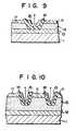
- the TFTmay have the structures shown in Figs. 9 and 10.
- parts like those shown in Fig. 1are designated by the same numerals.
- Fig. 9shows a U MOS or V MOS transistor structure, in which an active layer 13 is sandwiched between drain and source electrodes 11 and 12, and an insulating layer 14 has a U- or V-shape extending from the drain electrode to the source electrode.
- Fig. 10shows a SIT (static induction transistor) structure, in which an active layer 10 is sandwiched between drain and source electrodes 11 and 12, and a plurality of gate sections are provided.
- SITstatic induction transistor
- the above embodimentis designed such that capacitor 6 is charged by the drain current of the TFT and subsequently the image information signal is read out through switch 5. However, it may be arranged to convert the drain current of the TFT directly into a voltage signal.
Landscapes
- Physics & Mathematics (AREA)
- Electromagnetism (AREA)
- Solid State Image Pick-Up Elements (AREA)
- Light Receiving Elements (AREA)
- Thin Film Transistor (AREA)
Description
- The invention relates to a photosensor and, more particularly, to a photosensor suited for an image sensor.
- A photodiode using hydrogenated amorphous silicon (a-Si:H) film has been attracting attention as an image sensor element for a use in such an apparatus as an electronic copier and a facsimile apparatus. Since the a-Si:H film has high photosensitivity and can be easily made large in area, it is particularly suited for a contact type image sensor. In the Japanese Journal of Applied Physics Supplements (1983) supplement 15th Conf. pages 201-204 entitled "Amorphous Si:H Linear Image Sensor operated by a Si: H TFT Array" by F. Okumura et al. An image sensor is disclosed consisting of an a-Si:H photodiode array, a thin film transistor (TFT) array, a matrix circuit and an external circuit. The TFT array consists of a-Si:H inverted transistors formed on a common substrate with the photodiodes.
- From US-A-4461 956 a solid state photoelectric converter in known in which the photoelectric converting element, the transfer means and the transistors constituting the signal processing circuit section are constituted of this semiconductor films comprising preferably amorphous hydrogenated silicon.
- In JP-A-57 114 292 a thin film switching transistor is integrally formed on a photoelectric converter.
- An image sensor is formed by arranging a great number of photodiodes in line. The photodiode usually takes a sandwich structure in which an a-Si:H film is sandwiched between upper and lower electrodes. The lower electrode is made of chromium (Cr) or like, while the upper electrode is made of transparent, electrically conductive film such as indium tin oxide (ITO) film. In this structure, a Schottky barrier is formed at interface between the a-Si:H film and upper electrode, thus exhibiting a diode characteristic. The lower electrode services as a cathode electrode, and the upper electrode as an anode electrode.
- A large number of such photodiodes are formed in line on a substrate, thus constituting an image sensor. The anode of each photodiode is connected to the negative terminal of a DC power supply, and the cathode of the photodiode is connected through a charging switch to the positive terminal of the DC power supply. The cathode of the photodiode is connected through a charge readout switch to a common output amplifier. When the charging switch is turned on, inter- electrode capacitor of the photodiode is charged. When the charging switch is turned off, the inter- electrode capacitor is discharged in response to light incident on the anode electrode. Subsequently, the charge readout switch is turned on, so that a signal voltage across the capacitor is read out by the output amplifier.
- The signal voltage taken from the capacitor is proportional to the product of the light-receiving area, illumination intensity and storage time. The recent trend for higher operation speed and higher resolution calls for smaller light-receiving area and shorter storage time; for instance, a resolution of 16 bits/mm and a storage time of 1 msec. are required. The light receiving area of one photodiode corresponding to the resolution of 16 bits/mm is 3.91 x 10⁻³/mm2. In this case, the inter- electrode capacitance is approximately 0.2 pF. Under the conditions of a practical illumination intensity of 500 Ix and an internal quantum efficiency of 1, the maximum signal voltage is found to be approximately 6.8 V by calculation.
- The noise in the image sensor includes a switching noise component resulting from the switch element (i.e., transistor) and a dark current noise component based on dark current in the photodiode. While the switching noise is irrelevant to temperature, the dark current noise increases with temperature. At 40°C or below, the signal-to-noise ratio of the read-out signal is 38 dB at the most, which is insufficient in practice. Recently, a signal-to-noise ratio of 80 dB or above in a temperature range of 0 to 80°C is required in addition to the high operation speed and high resolution.
- As another prior art photosensor, a combination of a solar battery and a MOS transistor is known, as is disclosed in Japanese Patent early Publication No. 59-25280 published on February 9, 1984. In this structure, a solar battery using a-Si:H film is formed on a MOS transistor formed on a silicon substrate, connected between the gate and source of this transistor. The drain current of the MOS transistor is controlled by incident light on the solar battery. The substrate is made of silicon crystal, and cannot easily be made large. Therefore, the structure is not suited for a photosensor for use in an image sensor which requires a large area.
- An object of the invention is to provide an improved photosensor.
- Another object of the invention is to provide a photosensor which can realize a high signal-to-noise ratio.
- A further object of the invention is to provide an image sensor having a high resolution, a high operation speed and a high signal-to-noise ratio.
- A photosensor according to the invention comprises the features such as recited in the claims.
- The charging means includes a DC power supply, a charge switching element for coupling the DC power supply to the photodiode to charge the inter-electrode capacitance thereof. The charge switching element is formed of a thin film transistor, formed on the substrate adjacent to the thin film transistor and photodiode, which is turned on and off by an externally applied control signal.
- The detecting means includes a charge storage capacitor coupled to the thin film transistor and charged by the channel current thereof; an output amplifier for taking out an output signal of the photosensor; and a detection switching element for coupling the charge storage capacitor to the output amplifier, which is turned on and off by an externally applied control signal. The detecting switching element is formed of a thin film transistor, and the charge storage capacitor and detecting switching element are formed on the circuit substrate.
- This invention can be more fully understood from the following detailed description when taken in conjunction with the accompanying drawings, in which:
- Fig. 1 shows an arrangement of a photosensor embodying the invention;
- Fig. 2 is a circuit diagram of the photosensor shown in Fig. 1;
- Fig. 3 is a circuit diagram of an image sensor formed of photosensors shown in Fig. 1;
- Fig. 4 is a graph showing the relation between the signal-to-noise ratio of the drain current and gate-to-source voltage of a thin film transistor used in the photosensor according to the invention;
- Fig. 5 shows temperature dependency of a prior art photosensor and a photosensor according to the invention;
- Fig. 6 is a circuit diagram a photosensor according to another embodiment of the invention; and
- Figs. 7 to 10 show arrangements of other thin film transistors which may be used in the photosensor of this invention.
- Fig. 1 shows a photosensor of this invention, formed in a staggered configuration on a substrate. The
substrate 1 is an insulating plate having a smooth (i.e., lustrous) surface. More specifically, it is an alkali metal-free glass plate having an optically polished major surface. Aphotodiode 2 of a sandwich structure and a thin film transistor (TFT) 3 are formed on the major surface ofsubstrate 1, integrally and adjacent to each other. A charging transistor (TFT) 4 and a detection transistor (TFT) 5 are formed adjacent toTFT 3 onsubstrate 1. Acapacitor 6 is formed betweenTFTs 4 and 5. More specifically, TFT 3 has drain andsource electrodes substrate 1. Between drain andsource electrodes active layer 13 which consists of a-Si:H film, aninsulating layer 14 of SiNx, and agate electrode layer 15 consisting of, for instance, chromium. - Drain and
source electrodes H film 13 andSiNx film 14 may be formed by plasma CVD process, from 100% SiH4 gas and SiH4/N2 mixture gas, respectively.Gate insulating film 14 may be double-layer film made of a SiNx layer and a SiOx layer, with the SiNx layer provided on the side ofactive layer 13.Gate electrode 15 may be formed by PEP. Photodiode 2 has acathode electrode 16, which is formed of the same material and by the same process asgate electrode 15, on a portion ofdrain electrode layer 11 that is not covered withinsulating film 14 and on a portion ofinsulating film 14. a-Si:H film 17 is formed on a portion ofcathode electrode 16 overinsulating layer 14. Ananode electrode 18 consisting of transparent conductive film is formed on a-Si:H film 17 andinsulating layer 14 so as to partly contactgate electrode 15. As a result,photodiode 2 is formed which has a sandwich structure with the a-Si:H film sandwiched between the anode and cathode electrodes. Evidently,gate electrode 15 anddrain electrode 11 ofTFT 3 are electrically connected to respective anode andcathode electrodes photodiode 2. ITO may be used for a material of the transparent conductive film.Light 20 is incident on a-Si:H film 17 throughtransparent anode electrode 18 ofphotodiode 2. Since the TFT and photodiode are formed adjacent to each other on the substrate, a wiring capacitance can be greatly reduced, improving the signal-to-noise ratio.- Charging TFT 4,
detection TFT 5 andcapacitor 6 are formed integrally withphotodiode 2 andTFT 3 onsubstrate 1.Capacitor 6 is formed ofsource electrode layer 12, insulatingfilm 14 formed thereon, and electrode layer 21 formed on insulatingfilm 14. Electrode 21 is spaced apart fromgate electrode 15 ofTFT 3, and a-Si:H film 22 is formed between electrode layer 21 andgate electrode 15. An insulatinglayer 23 is formed on electrode layer 21, a-Si:H film 22 andgate electrode 15 ofTFT 3. Agate electrode 24 is formed on insulatingfilm 23. Thus, charging TFT 4 for charging the interelectrode capacitance ofphotodiode 2 is formed.Gate electrode 15 oftransistor 3 and electrode 21 ofcapacitor 6 are used as the drain and source electrodes of charging TFT 4, respectively. - An
electrode 24 is formed on the major surface ofsubstrate 1, and anactive layer 25, or a-Si:H layer, is formed betweenelectrodes layer 14 is formed to extend onelectrodes active layers gate electrode 26 is formed overactive layer 25 with insulatinglayer 14 interposed therebetween. In this way,detection TFT 5 is formed.Electrodes detection transistor 5, respectively. - A charging (i.e., reset) pulse and a readout pulse are applied to the gate electrodes of charging TFT 4 and
detection TFT 5, respectively. The positive terminal of apower supply 27 with 5 to 6 V is connected tocathode electrode 16 ofphotodiode 2, while the negative terminal of the power supply is connected to a common potential (i.e., ground) terminal. Capacitor electrode 21 is connected to a non-inverting input of anoutput amplifier 28, andsource electrode 24 ofdetection transistor 5 is connected to an inverting input ofamplifier 28.Amplifier 28 is provided separately from the photosensor circuit formed onsubstrate 1. - The operation of the photosensor shown in Fig. 1 will now be described with reference to Fig. 2, i.e., a circuit diagram thereof. Charging TFT (switch) 4 and detection TFT (switch) 5 are normally off. They are turned on by a charging pulse and a readout pulse from a control circuit (not shown), respectively. When a charging pulse turns charging TFT 4 on, the inter-electrode capacitance C of
photodiode 2 is charged bypower supply 27. At this time,TFT 3 is off since itsgate electrode 15 is coupled to electrode 21 placed at ground potential through the channel of conducting TFT 4. The drain current oftransistor 3 is a small off-current ID off. After chargingTFT 3 has been turned off, the inter-electrode capacitance C ofphotodiode 2 gradually discharges in accordance with photocurrent corresponding to the incidentimage information light 20. The discharging of inter-electrode capacitance C raises the potential ongate electrode 15 ofTFT 3. As a result, a drain current based on the gate potential flows inTFT 3.Capacitor 6 is charged by this drain current. The extent of chargingcapacitor 6 depends on the intensity of light 20 incident onphotodiode 2. - When the read-out pulse is applied to the gate electrode of
detection TFT 5,detection TFT 5 is turned on. As a result, the voltage acrosscapacitor 6 is applied tooutput amplifier 28, so that an output image information signal is obtained. - Fig. 3 shows a circuit diagram of an image sensor in which a plurality of photosensors as described above are arranged in a line. More specifically, in this image sensor, n photosensors, each of which corresponds to one picture element (i.e., one dot) and is constituted by a
photodiode 2, aTFT 3, a charging TFT 4, adetection TFT 5 and acapacitor 6, are arranged in line on a substrate. Each photosensor is wired in the manner as shown in Fig. 2. The n photosensors are successively enabled by control signals having charging pulses and read-out pulses. Thus, the image information signal is taken from anoutput amplifier 28. Where the resolution is 16 dots/mm, n is approximately 3,500. - Fig. 4 shows a relation between the signal-to-noise ratio of drain current ID of
TFT 3 and gate- source voltage V GS thereof. As is shown, the threshold voltage ofTFT 3 is 2 to 3 V, and the signal-to-noise ratio is not less than 100 dB with respect to the drain current when the V GS changes by several volts. The signal voltage taken out from the photodiode having the sandwich structure (i.e., voltage across the interelectrode capacitor) is 0 to 7 V when the intensity of the incident light is 0.5 Ix/sec. Thus, an output signal having a dynamic range of approximately 100 dB can be obtained by controlling the TFT gate voltage with the signal voltage from the photodiode and by detecting the drain current. Thus, an image information signal of a great signal-to-noise ratio can be obtained. Besides, the noise voltage, such as switching noise and dark current noise, is on the order of the threshold voltage of TFT. This indicates that the noise voltage tends to be compressed, to further improve the signal-to-noise ratio. - Fig. 5 shows the temperature-
dependency 41 of an output signal of a sandwich type photodiode consisting of a TFT and a photodiode, and also the temperature-dependency 42 of an output signal of the photosensor according to the invention. As is evident from Fig. 5, a signal-to-noise ratio of 80 dB or above can be realized in a temperature range of 0 to 80°C. This can meet the requirements of a high performance image sensor, i.e., the resolution of 16 dots/mm and the readout speed of 1 msec. - The modifications of this invention will be described hereinafter.
- The
substrate 1 may be made of glazed ceramic or organic film of a polyimide resin which can withstand a high temperature of 400°C. The active layer may be made of a-Si:H film or polycrystalline silicon film formed by a vacuum deposition process or sputtering process. The photodiode may have a pin structure or any other structure. - Further,
photodiode 2 may be connected between the gate electrode and sburce electrode ofTFT 3 as shown in Fig. 6. It suffices to connect the photodiode between the drain or source electrode a channel, and the gate electrode. (A channel is formed between the drain and source electrodes.) - The structure of the photodiode and TFT is not limited to the staggered structure shown in Fig. 1. Further, the positional relationship among drain and
source electrodes active layer 13, insulatinglayer 14 andgate electrode 15 of the TFT in the direction normal to the major surface of the substrate in Fig. 1 may be reversed as shown in Fig. 7. That is, an inverse staggered structure may be adopted. Further, the TFT may take coplanar structure in whichelectrodes active layer 13 as shown in Fig. 8. - Further, the TFT may have the structures shown in Figs. 9 and 10. In these Figures, parts like those shown in Fig. 1 are designated by the same numerals. Fig. 9 shows a U MOS or V MOS transistor structure, in which an
active layer 13 is sandwiched between drain andsource electrodes layer 14 has a U- or V-shape extending from the drain electrode to the source electrode. Fig. 10 shows a SIT (static induction transistor) structure, in which anactive layer 10 is sandwiched between drain andsource electrodes - The above embodiment is designed such that
capacitor 6 is charged by the drain current of the TFT and subsequently the image information signal is read out throughswitch 5. However, it may be arranged to convert the drain current of the TFT directly into a voltage signal.
Claims (5)
detecting means (5, 6, 28) are coupled to said thin film transistor (3) for detecting the channel current of said thin film transistor (3) which is controlled by a voltage across said inter-electrode capacitance of said photodiode (2), the voltage varying in response to the intensity of incident light (20) after said inter-electrode capacitance has been charged.
Applications Claiming Priority (2)
| Application Number | Priority Date | Filing Date | Title |
|---|---|---|---|
| JP59204806AJPS6182466A (en) | 1984-09-29 | 1984-09-29 | light sensor |
| JP204806/84 | 1984-09-29 |
Publications (3)
| Publication Number | Publication Date |
|---|---|
| EP0177275A2 EP0177275A2 (en) | 1986-04-09 |
| EP0177275A3 EP0177275A3 (en) | 1988-09-07 |
| EP0177275B1true EP0177275B1 (en) | 1990-06-13 |
Family
ID=16496670
Family Applications (1)
| Application Number | Title | Priority Date | Filing Date |
|---|---|---|---|
| EP85306847AExpired - LifetimeEP0177275B1 (en) | 1984-09-29 | 1985-09-26 | Photosensor suited for image sensor |
Country Status (5)
| Country | Link |
|---|---|
| US (1) | US4823178A (en) |
| EP (1) | EP0177275B1 (en) |
| JP (1) | JPS6182466A (en) |
| KR (1) | KR900006952B1 (en) |
| DE (1) | DE3578269D1 (en) |
Families Citing this family (39)
| Publication number | Priority date | Publication date | Assignee | Title |
|---|---|---|---|---|
| JP2569053B2 (en)* | 1987-06-26 | 1997-01-08 | キヤノン株式会社 | Image sensor |
| US4889983A (en)* | 1987-11-24 | 1989-12-26 | Mitsubishi Denki Kabushiki Kaisha | Image sensor and production method thereof |
| WO1991003745A1 (en)* | 1989-09-06 | 1991-03-21 | University Of Michigan | Multi-element-amorphous-silicon-detector-array for real-time imaging and dosimetry of megavoltage photons and diagnostic x-rays |
| JPH0734467B2 (en)* | 1989-11-16 | 1995-04-12 | 富士ゼロックス株式会社 | Image sensor manufacturing method |
| US6008078A (en)* | 1990-07-24 | 1999-12-28 | Semiconductor Energy Laboratory Co., Ltd. | Method for manufacturing a semiconductor device |
| AU1995092A (en)* | 1991-05-10 | 1992-12-30 | Q-Dot. Inc. | High-speed peristaltic ccd imager with gaas fet output |
| US5408113A (en)* | 1992-06-30 | 1995-04-18 | Ricoh Company, Ltd. | High sensitivity improved photoelectric imaging device with a high signal to noise ratio |
| KR100382817B1 (en)* | 1999-01-20 | 2003-05-09 | 엘지.필립스 엘시디 주식회사 | A pattern for detecting the living things and thin film transistor optical sensor with the same |
| US7053967B2 (en)* | 2002-05-23 | 2006-05-30 | Planar Systems, Inc. | Light sensitive display |
| US7023503B2 (en)* | 2002-02-20 | 2006-04-04 | Planar Systems, Inc. | Image sensor with photosensitive thin film transistors |
| US7009663B2 (en)* | 2003-12-17 | 2006-03-07 | Planar Systems, Inc. | Integrated optical light sensitive active matrix liquid crystal display |
| AU2002336341A1 (en)* | 2002-02-20 | 2003-09-09 | Planar Systems, Inc. | Light sensitive display |
| JP2003332560A (en)* | 2002-05-13 | 2003-11-21 | Semiconductor Energy Lab Co Ltd | Semiconductor device and microprocessor |
| JP4373063B2 (en) | 2002-09-02 | 2009-11-25 | 株式会社半導体エネルギー研究所 | Electronic circuit equipment |
| JP4094386B2 (en)* | 2002-09-02 | 2008-06-04 | 株式会社半導体エネルギー研究所 | Electronic circuit equipment |
| JP4574118B2 (en)* | 2003-02-12 | 2010-11-04 | 株式会社半導体エネルギー研究所 | Semiconductor device and manufacturing method thereof |
| US20080048995A1 (en)* | 2003-02-20 | 2008-02-28 | Planar Systems, Inc. | Light sensitive display |
| US20080084374A1 (en) | 2003-02-20 | 2008-04-10 | Planar Systems, Inc. | Light sensitive display |
| US7773139B2 (en)* | 2004-04-16 | 2010-08-10 | Apple Inc. | Image sensor with photosensitive thin film transistors |
| US20070109239A1 (en)* | 2005-11-14 | 2007-05-17 | Den Boer Willem | Integrated light sensitive liquid crystal display |
| JP5131508B2 (en)* | 2005-11-14 | 2013-01-30 | Nltテクノロジー株式会社 | Light receiving circuit |
| US7688947B2 (en)* | 2006-10-17 | 2010-03-30 | Varian Medical Systems, Inc. | Method for reducing sensitivity modulation and lag in electronic imagers |
| KR101441429B1 (en)* | 2007-09-21 | 2014-09-18 | 삼성디스플레이 주식회사 | Sensor thin film transistor and thin film transistor substrate having the same, method for manufacturing thin film transistor substrate |
| US9310923B2 (en) | 2010-12-03 | 2016-04-12 | Apple Inc. | Input device for touch sensitive devices |
| US8928635B2 (en) | 2011-06-22 | 2015-01-06 | Apple Inc. | Active stylus |
| US9329703B2 (en) | 2011-06-22 | 2016-05-03 | Apple Inc. | Intelligent stylus |
| US8638320B2 (en) | 2011-06-22 | 2014-01-28 | Apple Inc. | Stylus orientation detection |
| US8889461B2 (en) | 2012-05-29 | 2014-11-18 | Taiwan Semiconductor Manufacturing Company, Ltd. | CIS image sensors with epitaxy layers and methods for forming the same |
| US9176604B2 (en) | 2012-07-27 | 2015-11-03 | Apple Inc. | Stylus device |
| US9652090B2 (en) | 2012-07-27 | 2017-05-16 | Apple Inc. | Device for digital communication through capacitive coupling |
| US9557845B2 (en) | 2012-07-27 | 2017-01-31 | Apple Inc. | Input device for and method of communication with capacitive devices through frequency variation |
| US10048775B2 (en) | 2013-03-14 | 2018-08-14 | Apple Inc. | Stylus detection and demodulation |
| US10067580B2 (en) | 2013-07-31 | 2018-09-04 | Apple Inc. | Active stylus for use with touch controller architecture |
| FR3026893B1 (en)* | 2014-10-07 | 2018-01-12 | Saurea | PHOTOVOLTAIC EFFECT TRANSISTOR AND PHOTOVOLTAIC MOTOR WITH INCREASED POWER |
| US10067618B2 (en) | 2014-12-04 | 2018-09-04 | Apple Inc. | Coarse scan and targeted active mode scan for touch |
| US10474277B2 (en) | 2016-05-31 | 2019-11-12 | Apple Inc. | Position-based stylus communication |
| JP7241684B2 (en) | 2016-10-25 | 2023-03-17 | トリナミクス ゲゼルシャフト ミット ベシュレンクテル ハフツング | detector for optical detection of at least one object |
| CN107610604B (en)* | 2017-09-25 | 2020-03-17 | 上海九山电子科技有限公司 | LED chip, array substrate, display panel and display device |
| US12153764B1 (en) | 2020-09-25 | 2024-11-26 | Apple Inc. | Stylus with receive architecture for position determination |
Family Cites Families (15)
| Publication number | Priority date | Publication date | Assignee | Title |
|---|---|---|---|---|
| JPS5739582B2 (en)* | 1974-09-13 | 1982-08-21 | ||
| JPS5850030B2 (en)* | 1979-03-08 | 1983-11-08 | 日本放送協会 | Photoelectric conversion device and solid-state imaging plate using it |
| JPS55128884A (en)* | 1979-03-28 | 1980-10-06 | Hitachi Ltd | Semiconductor photodetector |
| JPS56135981A (en)* | 1980-03-28 | 1981-10-23 | Canon Inc | Photoelectric conversion element |
| DE3112907A1 (en)* | 1980-03-31 | 1982-01-07 | Canon K.K., Tokyo | "PHOTOELECTRIC SOLID BODY CONVERTER" |
| JPS56138965A (en)* | 1980-03-31 | 1981-10-29 | Canon Inc | Photoelectric converter |
| JPS5746224A (en)* | 1980-09-03 | 1982-03-16 | Canon Inc | Lens system equipped with auxiliary lens |
| US4471371A (en)* | 1981-01-06 | 1984-09-11 | Fuji Xerox Co., Ltd. | Thin film image pickup element |
| JPS57114292A (en)* | 1981-01-06 | 1982-07-16 | Fuji Xerox Co Ltd | Thin film image pickup element |
| US4517733A (en)* | 1981-01-06 | 1985-05-21 | Fuji Xerox Co., Ltd. | Process for fabricating thin film image pick-up element |
| JPS5922360A (en)* | 1982-07-28 | 1984-02-04 | Matsushita Electric Works Ltd | Optical input mos type transistor |
| JPS5925280A (en)* | 1982-07-31 | 1984-02-09 | Matsushita Electric Works Ltd | Optical input MOS transistor |
| US4651185A (en)* | 1983-08-15 | 1987-03-17 | Alphasil, Inc. | Method of manufacturing thin film transistors and transistors made thereby |
| JPS60103676A (en)* | 1983-11-11 | 1985-06-07 | Seiko Instr & Electronics Ltd | Method for manufacturing thin film transistor array |
| US4598305A (en)* | 1984-06-18 | 1986-07-01 | Xerox Corporation | Depletion mode thin film semiconductor photodetectors |
- 1984
- 1984-09-29JPJP59204806Apatent/JPS6182466A/enactivePending
- 1985
- 1985-09-24KRKR1019850007015Apatent/KR900006952B1/ennot_activeExpired
- 1985-09-26EPEP85306847Apatent/EP0177275B1/ennot_activeExpired - Lifetime
- 1985-09-26DEDE8585306847Tpatent/DE3578269D1/ennot_activeExpired - Lifetime
- 1985-09-26USUS06/780,598patent/US4823178A/ennot_activeExpired - Lifetime
Also Published As
| Publication number | Publication date |
|---|---|
| DE3578269D1 (en) | 1990-07-19 |
| KR860002741A (en) | 1986-04-28 |
| EP0177275A2 (en) | 1986-04-09 |
| US4823178A (en) | 1989-04-18 |
| KR900006952B1 (en) | 1990-09-25 |
| JPS6182466A (en) | 1986-04-26 |
| EP0177275A3 (en) | 1988-09-07 |
Similar Documents
| Publication | Publication Date | Title |
|---|---|---|
| EP0177275B1 (en) | Photosensor suited for image sensor | |
| US4862237A (en) | Solid state image sensor | |
| EP0855746B1 (en) | An image detector | |
| US4271420A (en) | Solid-state image pickup device | |
| US4461956A (en) | Solid-state photoelectric converter | |
| US5591963A (en) | Photoelectric conversion device with dual insulating layer | |
| US4894699A (en) | Optical control circuit and semiconductor device for realizing the circuit | |
| JPH05160379A (en) | Image sensor and image reading device | |
| US4549088A (en) | Original reading device | |
| EP0260824B1 (en) | Circuit for a photosensitive pixel with exposed blocking element | |
| Morozumi et al. | Completely integrated contact-type linear image sensor | |
| US4845355A (en) | Photoconductive type sensor and its driving method and apparatus | |
| US4876585A (en) | Contact type image sensor with separate charge transfer device | |
| US6031248A (en) | Hybrid sensor pixel architecture | |
| US6252215B1 (en) | Hybrid sensor pixel architecture with gate line and drive line synchronization | |
| US6005238A (en) | Hybrid sensor pixel architecture with linearization circuit | |
| Fischer et al. | Thin Film on ASIC-a novel concept for intelligent image sensors | |
| KR20000050791A (en) | Thin film transistor type photo sensor | |
| JP2921821B2 (en) | Photoelectric conversion device | |
| US20250103167A1 (en) | Optical touch detection circuit and optical touch display panel | |
| US6051827A (en) | Hybrid sensor pixel architecture with threshold response | |
| JPS61263156A (en) | Image sensor | |
| JPH06177417A (en) | Phototransistor and line image sensor | |
| JPH07109423B2 (en) | Image reader | |
| JP2781614B2 (en) | Contact type reading sensor |
Legal Events
| Date | Code | Title | Description |
|---|---|---|---|
| PUAI | Public reference made under article 153(3) epc to a published international application that has entered the european phase | Free format text:ORIGINAL CODE: 0009012 | |
| 17P | Request for examination filed | Effective date:19851010 | |
| AK | Designated contracting states | Kind code of ref document:A2 Designated state(s):DE FR GB | |
| PUAL | Search report despatched | Free format text:ORIGINAL CODE: 0009013 | |
| AK | Designated contracting states | Kind code of ref document:A3 Designated state(s):DE FR GB | |
| 17Q | First examination report despatched | Effective date:19881222 | |
| GRAA | (expected) grant | Free format text:ORIGINAL CODE: 0009210 | |
| AK | Designated contracting states | Kind code of ref document:B1 Designated state(s):DE FR GB | |
| REF | Corresponds to: | Ref document number:3578269 Country of ref document:DE Date of ref document:19900719 | |
| ET | Fr: translation filed | ||
| PLBE | No opposition filed within time limit | Free format text:ORIGINAL CODE: 0009261 | |
| STAA | Information on the status of an ep patent application or granted ep patent | Free format text:STATUS: NO OPPOSITION FILED WITHIN TIME LIMIT | |
| 26N | No opposition filed | ||
| REG | Reference to a national code | Ref country code:GB Ref legal event code:746 Effective date:19980915 | |
| REG | Reference to a national code | Ref country code:FR Ref legal event code:D6 | |
| PGFP | Annual fee paid to national office [announced via postgrant information from national office to epo] | Ref country code:FR Payment date:20000912 Year of fee payment:16 | |
| PGFP | Annual fee paid to national office [announced via postgrant information from national office to epo] | Ref country code:DE Payment date:20000918 Year of fee payment:16 | |
| PGFP | Annual fee paid to national office [announced via postgrant information from national office to epo] | Ref country code:GB Payment date:20000920 Year of fee payment:16 | |
| PG25 | Lapsed in a contracting state [announced via postgrant information from national office to epo] | Ref country code:GB Free format text:LAPSE BECAUSE OF NON-PAYMENT OF DUE FEES Effective date:20010926 | |
| REG | Reference to a national code | Ref country code:GB Ref legal event code:IF02 | |
| PG25 | Lapsed in a contracting state [announced via postgrant information from national office to epo] | Ref country code:DE Free format text:LAPSE BECAUSE OF NON-PAYMENT OF DUE FEES Effective date:20020501 | |
| GBPC | Gb: european patent ceased through non-payment of renewal fee | Effective date:20010926 | |
| PG25 | Lapsed in a contracting state [announced via postgrant information from national office to epo] | Ref country code:FR Free format text:LAPSE BECAUSE OF NON-PAYMENT OF DUE FEES Effective date:20020531 | |
| REG | Reference to a national code | Ref country code:FR Ref legal event code:ST |