EP0175378B1 - Dynamic random access memory (dram) - Google Patents
Dynamic random access memory (dram)Download PDFInfo
- Publication number
- EP0175378B1 EP0175378B1EP85111909AEP85111909AEP0175378B1EP 0175378 B1EP0175378 B1EP 0175378B1EP 85111909 AEP85111909 AEP 85111909AEP 85111909 AEP85111909 AEP 85111909AEP 0175378 B1EP0175378 B1EP 0175378B1
- Authority
- EP
- European Patent Office
- Prior art keywords
- transistor
- select transistor
- gate
- cell
- read select
- Prior art date
- Legal status (The legal status is an assumption and is not a legal conclusion. Google has not performed a legal analysis and makes no representation as to the accuracy of the status listed.)
- Expired - Lifetime
Links
Images


Classifications
- H—ELECTRICITY
- H10—SEMICONDUCTOR DEVICES; ELECTRIC SOLID-STATE DEVICES NOT OTHERWISE PROVIDED FOR
- H10B—ELECTRONIC MEMORY DEVICES
- H10B12/00—Dynamic random access memory [DRAM] devices
- H10B12/20—DRAM devices comprising floating-body transistors, e.g. floating-body cells
- H—ELECTRICITY
- H10—SEMICONDUCTOR DEVICES; ELECTRIC SOLID-STATE DEVICES NOT OTHERWISE PROVIDED FOR
- H10D—INORGANIC ELECTRIC SEMICONDUCTOR DEVICES
- H10D88/00—Three-dimensional [3D] integrated devices
- G—PHYSICS
- G11—INFORMATION STORAGE
- G11C—STATIC STORES
- G11C11/00—Digital stores characterised by the use of particular electric or magnetic storage elements; Storage elements therefor
- G11C11/21—Digital stores characterised by the use of particular electric or magnetic storage elements; Storage elements therefor using electric elements
- G11C11/34—Digital stores characterised by the use of particular electric or magnetic storage elements; Storage elements therefor using electric elements using semiconductor devices
- G11C11/40—Digital stores characterised by the use of particular electric or magnetic storage elements; Storage elements therefor using electric elements using semiconductor devices using transistors
- G11C11/401—Digital stores characterised by the use of particular electric or magnetic storage elements; Storage elements therefor using electric elements using semiconductor devices using transistors forming cells needing refreshing or charge regeneration, i.e. dynamic cells
- G11C11/403—Digital stores characterised by the use of particular electric or magnetic storage elements; Storage elements therefor using electric elements using semiconductor devices using transistors forming cells needing refreshing or charge regeneration, i.e. dynamic cells with charge regeneration common to a multiplicity of memory cells, i.e. external refresh
- G11C11/405—Digital stores characterised by the use of particular electric or magnetic storage elements; Storage elements therefor using electric elements using semiconductor devices using transistors forming cells needing refreshing or charge regeneration, i.e. dynamic cells with charge regeneration common to a multiplicity of memory cells, i.e. external refresh with three charge-transfer gates, e.g. MOS transistors, per cell
- H—ELECTRICITY
- H10—SEMICONDUCTOR DEVICES; ELECTRIC SOLID-STATE DEVICES NOT OTHERWISE PROVIDED FOR
- H10B—ELECTRONIC MEMORY DEVICES
- H10B12/00—Dynamic random access memory [DRAM] devices
- H—ELECTRICITY
- H10—SEMICONDUCTOR DEVICES; ELECTRIC SOLID-STATE DEVICES NOT OTHERWISE PROVIDED FOR
- H10B—ELECTRONIC MEMORY DEVICES
- H10B12/00—Dynamic random access memory [DRAM] devices
- H10B12/01—Manufacture or treatment
Definitions
- the present inventionrelates to dynamic random access memory (hereafter DRAM) devices.
- RAMRandom access memory
- MOSmetaloxide-transistor
- static MOS RAMsMOS RAMs
- dynamic MOS RAMsA static MOS memory (RAM) usually has a relatively high speed of operation and a rather higher power dissipation as compared with a dynamic memory circuit (RAM).
- DRAMdynamic MOS RAM
- DRAMsneed occupy less area on a substrate, being suitable for achieving high packing density, and has lesser power consumption, although its speed of operation is rather lower and more elaborate control circuits are required in comparison with a static RAM.
- DRAMsare increasingly used as storage devices of high capacity for electronic devices.
- a DRAM cell having only a single transistorhas been developed and widely used.
- Such a one transistor memory cellrequires only two control lines, a bit line and a word line.
- itrequires a sensitive sense amplifier, because an output signal of the cell is read out as a potential differential of the associated bit line provided by a stored charge in a capacitor of the cell.
- a greater part of the electrical charge stored in the cellis consumed to charge up the parasitic capacity of the bit line, which means that only a small potential differential can be attained: namely a very faint output signal.
- a three-transistor cellis one DRAM cell type recently proposed.
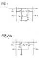
- Fig. 1is a schematic diagram of a previously proposed three-transistor memory cell, having a shared read/write (R/W) data bit line DL.
- the cellalso has a read select line RL and a separate write select line WL.
- informationis stored as the potential level of the gate of a storage transistor T3, which is generated in dependence upon stored charges in the gate electrode, and the stored information is output by making a read select transistor T1 conductive, for example so as to discharge the data bit line DL to ground potential when the storage transistor T3 is also conductive.
- an output signal potential differential(the difference between the voltage levels of the data bit line DL for different stored information values) can be substantially greater than the output signal potential differential available with a one-transistor cell.
- a simple sense-amplifieris sufficient to detect the output signal, which means that the sense-amplifier region can be reduced in size, providing a higher packing density in this respect.
- the numbers of transistors and lines used for a cellare larger than those used for a one-transistor cell. When these elements and lines are arranged in a plane, the cell occupies a relatively large area, adversely affecting the packing density of a device using such cells.
- EP-A-0 147 151published on 03.07.85, claiming priority from Japanese Patent Application JP 237776/83 dated 19.12.83, discloses a three-transistor dynamic random access memory which has a structure in which a write address transistor is stacked on a read address transistor.
- US-A-4 084 108discloses (Fig. 3B) what appears to be a form of dual gate MOS transistor.
- US-A-3 868 654discloses the use of a common read/write select line with transistors of different threshold voltages.
- a three-transistor cell for a dynamic random access memory formed on a semiconductor substratecomprising a read select transistor, having a drain connected to a data bit line of the memory, and a gate connected to a read select line of the memory, a storage transistor, having a drain connected to a source of the read select transistor and a source connected to a ground line of the memory, and a write select transistor, having a source connected to a gate of the storage transistor, a gate connected to a write select line of the memory, and a drain connected to the data bit line, characterised in that the read select transistor and the storage transistor are formed as a dual gate transistor, a channel region of the read select transistor being directly connected to a channel region of the storage transistor to provide a channel region of the dual gate transistor, the channel region of the read select transistor also acting as drain of the storage transistor and the channel region of the storage transistor also acting as source of the read select transistor, the drain of the read select transistor being the drain of the dual gate transistor and the source
- An embodiment of the present inventioncan provide a three-transistor cell for a DRAM having a structure enabling a higher packaging density to be achieved for the DRAM device.
- An embodiment of the present inventioncan provide a three-transistor cell for a DRAM with a two-storied structure wherein an arrangement of elements and associated control lines of the cell is provided which is effective to reduce the area of the cell.
- An embodiment of the present inventioncan provide a configuration for a three-transistor cell of a DRAM device which enables a reduction of the number of control lines from three to two (not including a ground line).
- An embodiment of the present inventionprovides a structure for a cell of a DRAM device wherein electrical elements are arranged in a two-storied configuration such that a high packing density can be realized.
- Embodiments of the present inventionprovide such two-storied structures of three transistor cells of DRAMS whereby the cells have either three or two driving lines besides a ground line.
- transistor T1 and transistor T3are both conductive when reading a stored signal "O", passing a current through the T1-T3 circuit between data bit line DL and ground line GND, but that transistor T1 is conductive and transistor T3 is non-conductive when a stored signal "1" is read and in this case no current flows through the T1-T3 circuit.
- a dual gate field effect transistorcan be applied in the cell of Fig. 1, by which the connection between transistor T1 and transistor T3 through respective source-drain regions can be omitted, serving to effect an economy as regards space on the relevant substrate of a DRAM device. This is applied in (some) embodiments of the present invention.
- two-storied or two-level structuresFor saving area on a substrate of a semiconductor device, two-storied or two-level structures have been utilized, wherein electronic elements are arranged in two layers separated from one another by an insulator layer.
- a read select transistor T1, a storage transistor T3, and a read select line RL which acts as a gate electrode of transistor T1are formed directly on the surface of a silicon substrate, i.e. on a first storey or level, whilst a write select transistor T2 and a write (word) select line WL which acts as a gate of transistor T2 are formed on a second storey, on an insulator layer separating the first and second stories.
- a data bit line DLis formed on a phospho-silicate glass layer covering the entire substrate.
- the arrangement of the transistorsis such that the write select transistor T2 overlies the read select transistor T1, and a common channel region is formed partially overlaid by the gates of read select transistor T1 and storage transistor T3.
- the transistors T1 and T3act like a dual gate transistor.
- the connecting portion between the two transistorsusually including at least source-drain regions, a remarkable saving is made.
- one of the source-drain regions of transistor T2is utilized also as the gate electrode of transistor T3, serving to save space on the substrate.
- a circuit configuration of a DRAM cellwherein the number of control lines of a memory cell is reduced from three to two; namely, a shared write/read bit line and a shared write/read select line, and two cell transistors having different threshold voltages from each other are used.
- a DRAM cell having a further simplified two-storied structureis provided in accordance with the circuit configuration of the cell.
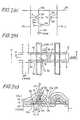
- Fig. 2 (a)is a circuit diagram of a memory cell of a DRAM; having three transistors and three control lines, whose configuration is quite similar to that of a previously proposed three transistor cell as shown in Fig. 1, except in relation to reference signs or indications Ch1, Ch3 denoting channel regions and in relation to reference signs or indications 3a, 3b, 9a and 9b denoting source-drain regions of respective transistors. These indications respectively correspond to those illustrated in the plan view of Fig. 2 (b) and the cross-sectional view of Fig. 2 (c).
- the gate electrode 5 of transistor T1is covered by an insulator layer 6 of Si02 having a thickness of approximately 6000 ⁇ , over which a write select transistor T2 is formed.
- the write select transistor T2 overlaid on the read select transistor T1comprises a first diffusion region 9a of n+ type (drain region), a second diffusion region 9b of n+ type (source region), a gate insulator 10 of Si02 having a thickness of approximately 300 ⁇ , a channel region Ch2 or 8 and a gate electrode 11.
- the silicon layer 8 of p typehas a thickness of 5000 to 8000 ⁇ , being formed using a silicon-on-insulator (SOI) technology.
- SOIsilicon-on-insulator
- the first diffusion region 9a and the second diffusion region 9bare formed in the silicon layer 8.
- the region 9areaches an insulator layer 7 of Si02 having a thickness of approximately 300 ⁇ and is connected to the drain region 3a of read select transistor T1 through a contact window 13a (Fig. 2 (c), see also 13 in Fig. 2 (b)).
- a storage transistor T3comprises the source region 3b, a drain region Ch1 which is used commonly with the read select transistor T1, the insulator layer 7 (as gate insulator), the channel region Ch3, and a gate electrode 9b which is commonly used as the source region of the write select transistor T2.
- the combined devicecomprising the read select transistor T1 and the storage transistor T3 can be regarded as a dual gate field effect transistor, comprising a drain region 3a, a source region 3b, a channel region Ch1 plus Ch3, two gate insulators 4,7 and two gate electrodes 5,9b.
- the write select transistor T2overlaying the write select transistor T2 over the read select transistor T1, one of the source region and the drain region of the transistor T2 is commonly used as the gate electrode of the storage transistor T3.
- the gate electrode 5 of the read select transistor T1 and the gate electrode 11 of the write select transistor T2are extended in a Y direction (indicated by an arrow marked Y in Fig. 2 (b)) to play the principless of a read select line RL and a word select line WL respectively.
- a phospho-silicate glass layer 12is formed to cover the transistors and lines of the device, and a data bit line DL 14 of aluminium is formed thereon in a direction perpendicular to the Y-direction, being connected to the drain regions 9a and 3a through a contact hole 13b (Fig. 2 (c), see also 13 in Fig. 2 (b)) opened in the phosphosilicate glass layer 12.
- the source region 3bis extended to serve as a ground line GND as shown in the plan view of Fig. 2 (b).
- the circuit configuration shown in Fig. 2 (a)is realized.
- the data bit line DLis maintained at a high level and the write select line WL, namely the gate electrode 11 of the write select transistor T2, is brought to a higher voltage level to make the write select transistor T2 "ON", bringing the gate electrode 9b of the storage transistor T3 to high level to keep the transistor T3 in "ON” state. Thereafter, the write select transistor T2 is made “OFF” to keep the voltage level of the gate electrode 9b of the storage transistor T3 high, storing the logical "O".
- the data bit line DLWhen reading a stored logical "O" from the cell, the data bit line DL is brought to a predetermined voltage level such as an intermediate voltage Vm level between high level and low level and kept floating. Thereafter, the read select transistor T1 is made “ON". Since the storage transistor T3 is in an "ON" state, a current flows from the data bit line DL to the ground line GND through the read select transistor T1 and the storage transistor T3 substantially pulling down the voltage of the data bit line DL to the ground voltage. The reduction of the voltage of the data bit line DL represents the logical "O".
- the data bit line DLis maintained at a low voltage level, and simultaneously the write select transistor T2 is made “ON”, making the voltage level of the gate of the storage transistor T3 low. Then, the write select transistor T2 is made “OFF” thereafter, maintaining the gate voltage level of the storage transistor T3 low, namely, maintaining the storage transistor T3 in "OFF" state.
- the data bit line DLWhen reading out the logical “l” from the cell, the data bit line DL is maintained at the voltage level Vm, for instance, and the read select transistor T1 is made “ON". Since the storage transistor T3 is "OFF" state, no current flows through the circuit storage transistor T3 plus read select transistor T1, maintaining the voltage of the data bit line DL at Vm, providing no voltage difference (no pull-down of the data bit line voltage) which represents the logical "1".
- the circuitry of the first embodiment of the present inventionoperates in the same manner as that of a previously prepared DRAM cell.
- the storage transistor T3 and the read select transistor T1co-possess their channel regions Ch3 and Ch1, eliminating diffusion regions for connecting the two transistors.
- one of the source-drain regions of the write select transistor T2is commonly used as the gate electrode of the storage transistor T3. As the result, a remarkable reduction in cell area can be achieved, enabling packing density to be increased significantly.
- the gate electrode 9b of the storage transistor T3 wherein information is stored in the form of electrical chargesis electrically isolated from the substrate 1 by the surrounding silicon dioxide layer 6 and 7, resulting in an effect which serves for preventing soft error problems, due to alpha ray irradiation.
- circuit configuration of Fig. 2 (a)can be illustrated in another configuration as shown in Fig. 2 (d), wherein the read select transistor T1 and the storage transistor T3 are replaced by a dual-gate electrode MOS transistor T d . It will be apparent from the above description of the first embodiment of the present invention, for those skilled in the art, that both circuit configurations are entirely the same with regard to circuit operation.
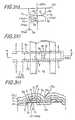
- the memory cell of the second embodimenthas three transistors and two control lines as shown in the circuit diagram of Fig. 3 (a).
- the read select line RL and write select line WL of Fig. 2 (a)are replaced by a single line, write/read select line WRL to which the gate electrodes of a write select transistor T2 and read select transistor T1 are connected. Therefore, in order to distinguish these two transistors from each other, the threshold voltages of the two transistors T1 and T2, namely V th1 and V th2 respectively, are made different from each other.
- control linesare reduced by one, and the resulting cell structure is further simplified.
- Fig. 3 (b)is a partial plan view of a DRAM device, illustrating the configuration of a memory cell in accordance with the second embodiment
- Fig. 3 (c)is a cross-sectional view of the cell taken along the line A-A shown in the partial plan view of Fig. 3 (b).
- Threshold voltages of transistors T1, T2 and T3are designated by V th1 , V th2 and V th3 respectively, and voltage levels of write/read select line WRL for selecting a reading or a writing operation are designated by V r and V w respectively.
- the voltage level of the data bit line DL, namely a data signalis designated by V d .
- T2When writing an information signal (e.g. "0" or "1") into the cell, T2 is made conductive by holding the write/read select line WRL at V w . Thereafter, an input signal voltage, 0 volt or V d , is applied to the data bit line DL, namely, to the gate of T3, depending on the input logical value to be written, resulting in an "OFF" state or an “ON” state of the storage transistor T3.
- the read select transistor T1is made also conductive simultaneously.
- the data signalis 0 volt, no current flows through T1-T3 line since storage transistor T3 is in an "OFF" state and no problem occurs.
- said read select transistor (T1) and said write select transistor (T2) formed over said read select transistor (T1)share a common gate electrode (15 - Fig. 3(c)) with each other, said common gate electrode (15) being disposed between said read select transistor (T1) and said write select transistor (T2) and effective for the respective transistors through respective gate insulator layers (4, 10).
- the side walls of the common gate electrode (15)are covered by insulating layers.
- two-storied structures and circuit configurations in accordance with the present inventioncan provide for high packing densities in associated DRAM devices.
- the present inventionserves to provide a DRAM device with easier fabricating processes, thereby serving to reduce manufacturing costs.
- a p-type silicon substrate 1is prepared, and field oxide layers FOX of silicon dioxide (Si02) are formed thereon by a conventional method, defining transistor regions A cell , being followed by the further formation of a first gate insulator layer 4 approximately 300 ⁇ thick over the transistor regions A cell by a conventional thermal oxidizing method.
- a tungsten silicide (WSi2) layer 5approximately 2000 ⁇ thick and an Si02 layer 6 approximately 5000 to 8000 ⁇ thick are formed subsequently by conventional chemical vapour deposition (CVD).
- CVDchemical vapour deposition
- a gate electrode 5 for read select transistor T1having Si02 insulator layer 6 thereon, is formed.
- the gate electrode 5is extended over the substrate and plays a consideration as a read select line RL.
- a photoresist mask R(indicated by broken lines in Fig. 5 (a)) is formed to cover the area on the substrate except for predetermined regions for data bit lines.
- arsenic (As) ionsare implanted into the exposed areas of the silicon substrate with a dose of 5X1015cm ⁇ 2 and an accelerating energy of 100 KeV, this being followed by removal of the photoresist mask R and by appropriate heat processing for diffusing the implanted As dopants to form a n+ type drain region 3a.
- the exposed surface(uncovered by the patterned gate electrode 5 on the Si02 layer (the gate insulator layer 4)) is etched off by a conventional wet etching method.
- a second gate insulator layer of Si02 approximately 300 ⁇ thickis formed by a conventional thermal oxidizing method.
- Si02approximately 500 ⁇ is formed on the side wall of the gate electrode 5.
- a contact window 13ais opened in the second gate insulator layer 7 over the n+ type drain region 3a, this being followed by the formation of a thick polycrystalline silicon layer 8 approximately 5000 ⁇ thick over the entire surface of the substrate 1.
- the polycrystalline silicon layeris converted to a single crystal layer by irradiation with a laser beam or an electron beam having a predetermined energy for heating.
- Thisis one of the SOI (silicon on insulator) technologies and the single crystal silicon layer is referred to as an SOI layer 8 which serves to form an MOS FET having a small gate leakage current.
- the SOI layer 8is doped, to become a p-type diffusion layer with 1016 cm ⁇ 3 dopant density, by boron (B+) ion implantation and subsequent heat treatment.
- a polycrystalline silicon layer formed on the entire substrate by a conventional CVD methodmay be converted into a layer of single crystal silicon structure by re-crystallization using a heat treatment at approximately 600 °C whereby the exposed single crystal structure of the contact region acts as seed for the recrystallization.
- a third gate insulator region 10approximately 300 ⁇ thick is formed by a thermal oxidizing method.
- This stepis followed by a chemical vapour deposition (CVD) process to form a tungsten silicide (WSi2) layer of approximately 2000 ⁇ thickness, accompanied by a photolithographic process for patterning a gate electrode 11 of a write select transistor T2.
- the gate electrode 11is extended to play a theme as a word select line WL.
- the next stepis ion implantation of arsenic ions (As+) with approximately 5X10¹⁵ dose and with an accelerating energy of approximately 120 KeV over the entire substrate, followed by a predetermined heat treatment, forming a first n+ type region 9a as a drain region of write select transistor T2, a second n+ region 9b as a source region of write select transistor T2, and an n+ type source region 3b.
- the source region 3b of storage transistor T3is extended to act as a ground line.
- the above-described n+ type regions 9a and 9bare formed to reach the underlying SOI layer 8.
- a contact window 13bis formed to expose the underlying drain region 3a of read select transistor T1.
- a data bit line DL of aluminium or other metalis formed over the phosphosilicate glass layer 12 so that the data bit line DL is connected to the drain region 9a of write select transistor T2 and the drain region 3a of read select transistor T1 through the contact window 13b.
- formation of a passivating layer for the substrate and other final processesare performed to complete the semiconductor memory device.
- a dynamic random access memory (DRAM) cellhaving three MIS transistors arranged in two-storied layers having a high packing density configuration is disclosed.
- a write select transistoris disposed overlying a read select transistor, being electrically separated from each other through an insulator layer, and a drain region of the write select transistor is shared with the underlying read select transistor as its gate electrode.
- a storage transistor and the read select transistorare formed on a silicon substrate in the same level and channel regions of both transistors are connected to each other and used as a diffusion region of the opposite transistor, resulting in elimination of connecting members such as diffusion regions and a conducting path therebetween which were otherwise necessary. These two points contribute to elevate the packing density of the cell.
- a write select line and a read select lineare combined into a single control line: write/read select line, saving one line to obtain higher packing density.
- gate electrodes of both transistorsare connected to the write/read line. These transistors are distinguished from each other by their different threshold voltage levels from each other.
Landscapes
- Engineering & Computer Science (AREA)
- Microelectronics & Electronic Packaging (AREA)
- Computer Hardware Design (AREA)
- Manufacturing & Machinery (AREA)
- Semiconductor Memories (AREA)
- Dram (AREA)
- Metal-Oxide And Bipolar Metal-Oxide Semiconductor Integrated Circuits (AREA)
- Recrystallisation Techniques (AREA)
Description
- The present invention relates to dynamic random access memory (hereafter DRAM) devices.
- Random access memory (RAM) devices made using metaloxide-transistor (MOS) technology have been used widely in storage apparatuses of electronic devices such as computers. For RAM devices, there have been used two different techniques for storing information: namely there have been provided static MOS RAMs and dynamic MOS RAMs. A static MOS memory (RAM) usually has a relatively high speed of operation and a rather higher power dissipation as compared with a dynamic memory circuit (RAM). On the other hand, a dynamic MOS RAM (DRAM) need occupy less area on a substrate, being suitable for achieving high packing density, and has lesser power consumption, although its speed of operation is rather lower and more elaborate control circuits are required in comparison with a static RAM. DRAMs are increasingly used as storage devices of high capacity for electronic devices.
- A great deal of effort has been made towards increasing the high packing density of DRAMS, resulting in reduction of the number of transistors per DRAM memory cell. Ultimately, a DRAM cell having only a single transistor has been developed and widely used. Such a one transistor memory cell requires only two control lines, a bit line and a word line. However, it requires a sensitive sense amplifier, because an output signal of the cell is read out as a potential differential of the associated bit line provided by a stored charge in a capacitor of the cell. When the cell is read out, a greater part of the electrical charge stored in the cell is consumed to charge up the parasitic capacity of the bit line, which means that only a small potential differential can be attained: namely a very faint output signal. Moreover, there is a tendency for the capacity of such a memory cell to be decreased, and for the parasitic capacity of the relevant data bit line to remain almost unchanged, as the packing density of the DRAM is increased. Thus, high sensitivity is increasingly required for the associated sense-amplifier, causing cost increase and reduction of packing density of a DRAM device.
- There have been proposed other types of DRAM cells, intended to overcome the above-described disadvantages of a one-transistor cell. A three-transistor cell is one DRAM cell type recently proposed.
- Fig. 1 is a schematic diagram of a previously proposed three-transistor memory cell, having a shared read/write (R/W) data bit line DL. The cell also has a read select line RL and a separate write select line WL. In a cell of this type, information is stored as the potential level of the gate of a storage transistor T₃, which is generated in dependence upon stored charges in the gate electrode, and the stored information is output by making a read select transistor T₁ conductive, for example so as to discharge the data bit line DL to ground potential when the storage transistor T₃ is also conductive. Thus, an output signal potential differential (the difference between the voltage levels of the data bit line DL for different stored information values) can be substantially greater than the output signal potential differential available with a one-transistor cell. Thus, a simple sense-amplifier is sufficient to detect the output signal, which means that the sense-amplifier region can be reduced in size, providing a higher packing density in this respect. However, with a three transistor cell, the numbers of transistors and lines used for a cell are larger than those used for a one-transistor cell. When these elements and lines are arranged in a plane, the cell occupies a relatively large area, adversely affecting the packing density of a device using such cells.
- EP-A-0 147 151, published on 03.07.85, claiming priority from Japanese Patent Application JP 237776/83 dated 19.12.83, discloses a three-transistor dynamic random access memory which has a structure in which a write address transistor is stacked on a read address transistor.
- US-A-4 084 108 discloses (Fig. 3B) what appears to be a form of dual gate MOS transistor.
- US-A-3 868 654 discloses the use of a common read/write select line with transistors of different threshold voltages.
- According to the present invention there is provided a three-transistor cell for a dynamic random access memory formed on a semiconductor substrate, the cell comprising
a read select transistor, having a drain connected to a data bit line of the memory, and a gate connected to a read select line of the memory,
a storage transistor, having a drain connected to a source of the read select transistor and a source connected to a ground line of the memory, and
a write select transistor, having a source connected to a gate of the storage transistor, a gate connected to a write select line of the memory, and a drain connected to the data bit line,
characterised in that
the read select transistor and the storage transistor are formed as a dual gate transistor, a channel region of the read select transistor being directly connected to a channel region of the storage transistor to provide a channel region of the dual gate transistor, the channel region of the read select transistor also acting as drain of the storage transistor and the channel region of the storage transistor also acting as source of the read select transistor, the drain of the read select transistor being the drain of the dual gate transistor and the source of the storage transistor being the source of the dual gate transistor, between which drain and source the channel region of the dual gate transistor lies, and the two gates of the dual gate transistor being, respectively, the gate of the read select transistor and the gate of the storage transistor, which gates overlie the channel region of the dual gate transistor via an interposed insulator layer,
and characterised in that
the write select transistor is formed over the read select transistor, with an interposed insulator layer, the drain of the write select transistor being connected directly to the drain of the read select transistor through a window or opening in the latter interposed insulator layer,
and in that
the source region of the write select transistor acts also as the gate of the storage transistor which is otherwise provided on the same side of the latter interposed insulator layer as the read select transistor. - An embodiment of the present invention can provide a three-transistor cell for a DRAM having a structure enabling a higher packaging density to be achieved for the DRAM device.
- An embodiment of the present invention can provide a three-transistor cell for a DRAM with a two-storied structure wherein an arrangement of elements and associated control lines of the cell is provided which is effective to reduce the area of the cell.
- An embodiment of the present invention can provide a configuration for a three-transistor cell of a DRAM device which enables a reduction of the number of control lines from three to two (not including a ground line).
- An embodiment of the present invention provides a structure for a cell of a DRAM device wherein electrical elements are arranged in a two-storied configuration such that a high packing density can be realized.
- Embodiments of the present invention provide such two-storied structures of three transistor cells of DRAMS whereby the cells have either three or two driving lines besides a ground line.
- In the above description of the previously proposed three-transistor memory cell shown in Fig. 1, it should be noted that transistor T₁ and transistor T₃ are both conductive when reading a stored signal "O", passing a current through the T₁-T₃ circuit between data bit line DL and ground line GND, but that transistor T₁ is conductive and transistor T₃ is non-conductive when a stored signal "1" is read and in this case no current flows through the T₁-T₃ circuit.
- The inventor has appreciated that a dual gate field effect transistor can be applied in the cell of Fig. 1, by which the connection between transistor T₁ and transistor T₃ through respective source-drain regions can be omitted, serving to effect an economy as regards space on the relevant substrate of a DRAM device. This is applied in (some) embodiments of the present invention.
- For saving area on a substrate of a semiconductor device, two-storied or two-level structures have been utilized, wherein electronic elements are arranged in two layers separated from one another by an insulator layer.
- In an embodiment of the present invention, a read select transistor T₁, a storage transistor T₃, and a read select line RL which acts as a gate electrode of transistor T₁ are formed directly on the surface of a silicon substrate, i.e. on a first storey or level, whilst a write select transistor T₂ and a write (word) select line WL which acts as a gate of transistor T₂ are formed on a second storey, on an insulator layer separating the first and second stories. A data bit line DL is formed on a phospho-silicate glass layer covering the entire substrate.
- In a DRAM memory cell in accordance with an embodiment of the present invention, the arrangement of the transistors is such that the write select transistor T₂ overlies the read select transistor T₁, and a common channel region is formed partially overlaid by the gates of read select transistor T₁ and storage transistor T₃. Thus the transistors T₁ and T₃ act like a dual gate transistor. As a result, in respect of the connecting portion between the two transistors, usually including at least source-drain regions, a remarkable saving is made. In addition, due to the overlying structure of transistor T₂ on transistor T₁ and the circuit configuration of the cell, one of the source-drain regions of transistor T₂ is utilized also as the gate electrode of transistor T₃, serving to save space on the substrate.
- Furthermore, in accordance with an embodiment of the present invention, a circuit configuration of a DRAM cell is provided wherein the number of control lines of a memory cell is reduced from three to two; namely, a shared write/read bit line and a shared write/read select line, and two cell transistors having different threshold voltages from each other are used. A DRAM cell having a further simplified two-storied structure is provided in accordance with the circuit configuration of the cell.
- Reference is made, by way of example, to the accompanying drawings, in which:-
- Fig. 1 is a schematic circuit diagram of a previously proposed three transistor DRAM cell;
- Fig. 2 (a) is a schematic circuit diagram of a three-transistor DRAM cell in accordance with a first embodiment of the present invention;
- Fig. 2 (b) is a partial plan view illustrating the structure of the three transistor cell of Fig. 2 (a);
- Fig. 2 (c) is a cross-sectional view of the cell of Fig. 2 (b), taken along the line A-A in Fig. 2 (b), illustrating the two-storey or two-level structure of the cell;
- Fig. 2 (d) is a schematic circuit diagram, equivalent to that of Fig. 2 (a), introducing the concept of a dual gate field effect transistor;
- Fig. 3 (a) is a schematic circuit diagram of a three-transistor DRAM cell in accordance with a second embodiment of the present invention, having a reduced number of driving lines as compared with the cell of Fig. 2 (a);
- Fig. 3 (b) is a partial plan view illustrating the structure of the three transistor cell of Fig. 3 (a);
- Fig. 3 (c) is a cross-sectional view of the three transistor cell of Fig. 3 (b), taken along the line A-A in Fig. 3 (b), illustrating the two-storey structure of the cell;
- Fig. 4 is a plan view of a cell in accordance with the first embodiment of the present invention illustrating the location of the cross-sectional views given in Fig. 5 (a) to Fig. 5 (e); and
- Figs. 5 (a) to 5 (e) are respective cross-sectional views relating to the cell of Fig. 4, taken along the line A-A shown in the plan view of Fig. 4, illustrating in sequence fabrication steps in the manufacture of a cell in accordance with the first embodiment of the present invention;
- Fig. 5 (a) illustrates formation of a gate electrode and a diffusion region;
- Fig. 5 (b) illustrates p-type doping of a SOI layer covering a substrate;
- Fig. 5 (c) illustrates formation of a further gate electrode;
- Fig. 5 (d) illustrates a n-type ion-implantation process for forming a diffused region; and
- Fig. 5 (e) illustrates the cell after formation of a data bit line.
- Referring to Figs. 2 (a) to 2 (c), there is shown a memory cell in accordance with a first embodiment of the present invention. Fig. 2 (a) is a circuit diagram of a memory cell of a DRAM; having three transistors and three control lines, whose configuration is quite similar to that of a previously proposed three transistor cell as shown in Fig. 1, except in relation to reference signs or indications Ch1, Ch3 denoting channel regions and in relation to reference signs or
indications - On a p-
type silicon substrate 1,field oxide layers 2, shown in the plan view of Fig. 2 (b) by hatching, are formed defining transistor regions and ground lines therebetween. In thesubstrate 1, a n+type drain region 3a and a n+type source region 3b are formed, having a channel region Ch1 plus Ch3 therebetween. A MOS transistor T₁, namely a read select transistor, comprises thedrain region 3a, channel region Ch1, channel region Ch3 as its source region, a channel (gate)insulator layer 4 of silicon dioxide (Si0₂) approximately 300 Å (1Å = 0.1 nm) thick formed over the channel region Ch1, and agate electrode 5 made of tungsten-silicide (WSi₂) or polycrystalline silicon, for instance. Thegate electrode 5 of transistor T₁ is covered by aninsulator layer 6 of Si0₂ having a thickness of approximately 6000 Å, over which a write select transistor T₂ is formed. - The write select transistor T₂ overlaid on the read select transistor T₁ comprises a
first diffusion region 9a of n+ type (drain region), asecond diffusion region 9b of n+ type (source region), agate insulator 10 of Si0₂ having a thickness of approximately 300 Å, a channel region Ch2 or 8 and agate electrode 11. Thesilicon layer 8 of p type has a thickness of 5000 to 8000 Å, being formed using a silicon-on-insulator (SOI) technology. Thefirst diffusion region 9a and thesecond diffusion region 9b are formed in thesilicon layer 8. Theregion 9a reaches aninsulator layer 7 of Si0₂ having a thickness of approximately 300 Å and is connected to thedrain region 3a of read select transistor T₁ through acontact window 13a (Fig. 2 (c), see also 13 in Fig. 2 (b)). - A storage transistor T₃ comprises the
source region 3b, a drain region Ch1 which is used commonly with the read select transistor T₁, the insulator layer 7 (as gate insulator), the channel region Ch3, and agate electrode 9b which is commonly used as the source region of the write select transistor T₂. - Thus, the combined device comprising the read select transistor T₁ and the storage transistor T₃ can be regarded as a dual gate field effect transistor, comprising a
drain region 3a, asource region 3b, a channel region Ch1 plus Ch3, twogate insulators gate electrodes - The
gate electrode 5 of the read select transistor T₁ and thegate electrode 11 of the write select transistor T₂ are extended in a Y direction (indicated by an arrow marked Y in Fig. 2 (b)) to play the rôles of a read select line RL and a word select line WL respectively. A phospho-silicate glass layer 12 is formed to cover the transistors and lines of the device, and a databit line DL 14 of aluminium is formed thereon in a direction perpendicular to the Y-direction, being connected to thedrain regions phosphosilicate glass layer 12. Thesource region 3b is extended to serve as a ground line GND as shown in the plan view of Fig. 2 (b). Thus the circuit configuration shown in Fig. 2 (a) is realized. - To write a logical "O" into the cell, the data bit line DL is maintained at a high level and the write select line WL, namely the
gate electrode 11 of the write select transistor T₂, is brought to a higher voltage level to make the write select transistor T₂ "ON", bringing thegate electrode 9b of the storage transistor T₃ to high level to keep the transistor T₃ in "ON" state. Thereafter, the write select transistor T₂ is made "OFF" to keep the voltage level of thegate electrode 9b of the storage transistor T₃ high, storing the logical "O". - When reading a stored logical "O" from the cell, the data bit line DL is brought to a predetermined voltage level such as an intermediate voltage Vm level between high level and low level and kept floating. Thereafter, the read select transistor T₁ is made "ON". Since the storage transistor T₃ is in an "ON" state, a current flows from the data bit line DL to the ground line GND through the read select transistor T₁ and the storage transistor T₃ substantially pulling down the voltage of the data bit line DL to the ground voltage. The reduction of the voltage of the data bit line DL represents the logical "O".
- For writing a logical "l" into the cell, the data bit line DL is maintained at a low voltage level, and simultaneously the write select transistor T₂ is made "ON", making the voltage level of the gate of the storage transistor T₃ low. Then, the write select transistor T₂ is made "OFF" thereafter, maintaining the gate voltage level of the storage transistor T₃ low, namely, maintaining the storage transistor T₃ in "OFF" state.
- When reading out the logical "l" from the cell, the data bit line DL is maintained at the voltage level Vm, for instance, and the read select transistor T₁ is made "ON". Since the storage transistor T₃ is "OFF" state, no current flows through the circuit storage transistor T₃ plus read select transistor T₁, maintaining the voltage of the data bit line DL at Vm, providing no voltage difference (no pull-down of the data bit line voltage) which represents the logical "1".
- As described above, the circuitry of the first embodiment of the present invention operates in the same manner as that of a previously prepared DRAM cell. However, the storage transistor T₃ and the read select transistor T₁ co-possess their channel regions Ch3 and Ch1, eliminating diffusion regions for connecting the two transistors. Furthermore, one of the source-drain regions of the write select transistor T₂ is commonly used as the gate electrode of the storage transistor T₃. As the result, a remarkable reduction in cell area can be achieved, enabling packing density to be increased significantly.
- In addition, the
gate electrode 9b of the storage transistor T₃ wherein information is stored in the form of electrical charges, is electrically isolated from thesubstrate 1 by the surroundingsilicon dioxide layer - The circuit configuration of Fig. 2 (a) can be illustrated in another configuration as shown in Fig. 2 (d), wherein the read select transistor T₁ and the storage transistor T₃ are replaced by a dual-gate electrode MOS transistor Td. It will be apparent from the above description of the first embodiment of the present invention, for those skilled in the art, that both circuit configurations are entirely the same with regard to circuit operation.
- Now, a second embodiment in accordance with the present invention will be described with reference to Figs. 3 (a) to 3 (c). The memory cell of the second embodiment has three transistors and two control lines as shown in the circuit diagram of Fig. 3 (a). In comparison with the cell of Fig. 2 (a), the read select line RL and write select line WL of Fig. 2 (a) are replaced by a single line, write/read select line WRL to which the gate electrodes of a write select transistor T₂ and read select transistor T₁ are connected. Therefore, in order to distinguish these two transistors from each other, the threshold voltages of the two transistors T₁ and T₂, namely Vth1 and Vth2 respectively, are made different from each other. Thus control lines are reduced by one, and the resulting cell structure is further simplified.
- Fig. 3 (b) is a partial plan view of a DRAM device, illustrating the configuration of a memory cell in accordance with the second embodiment, and Fig. 3 (c) is a cross-sectional view of the cell taken along the line A-A shown in the partial plan view of Fig. 3 (b).
- Threshold voltages of transistors T₁, T₂ and T₃ are designated by Vth1, Vth2 and Vth3 respectively, and voltage levels of write/read select line WRL for selecting a reading or a writing operation are designated by Vr and Vw respectively. The voltage level of the data bit line DL, namely a data signal is designated by Vd.
- Taking the threshold voltage of storage transistor T₃ as Vth3=Vth1, the relationships required for the above threshold voltage levels are as follows:


- When writing an information signal (e.g. "0" or "1") into the cell, T₂ is made conductive by holding the write/read select line WRL at Vw. Thereafter, an input signal voltage, 0 volt or Vd, is applied to the data bit line DL, namely, to the gate of T₃, depending on the input logical value to be written, resulting in an "OFF" state or an "ON" state of the storage transistor T₃. In this circuit configuration, the read select transistor T₁ is made also conductive simultaneously. When the data signal is 0 volt, no current flows through T₁-T₃ line since storage transistor T₃ is in an "OFF" state and no problem occurs. However, when the data signal is Vd, a current flows from the data bit line DL to the ground line GND, which has an adverse effect so far as holding the voltage of the data bit line DL at Vd is concerned. Therefore, in order to maintain the voltage level Vd of the DL line, it is necessary to make the equivalent resistance of the associated driving circuit of the data bit line DL substantially lower than that of the series resistance of the T₁-T₃ circuit.
- When reading out a stored signal from the cell, the voltage of the write/read select line WRL is held at Vr, making read select transistor T₁ "ON" and write select transistor T₂ "OFF" due to the condition of Vr as described above. Therefore, the voltage of the gate of the storage transistor T₃ is maintained unchanged. Thus, when the stored signal, namely, the voltage of the gate of storage transistor T₃ is 0 volt, no current flows from the data bit line DL to the ground line GND since T₃ is in "OFF" state. Accordingly, the voltage of the data bit line DL is maintained unchanged, and is output through a sense amplifier to represent an information signal "l". When the stored signal is Vd, making storage transistor T₃ conductive, charges in the data bit line DL flow to the ground line GND, resulting in a substantial fall in the voltage of the data bit line DL, which is output through the sense amplifier to represent an information signal "0".
- As seen particularly in Fig. 3(c), said read select transistor (T₁) and said write select transistor (T₂) formed over said read select transistor (T₁) share a common gate electrode (15 - Fig. 3(c)) with each other, said common gate electrode (15) being disposed between said read select transistor (T₁) and said write select transistor (T₂) and effective for the respective transistors through respective gate insulator layers (4, 10). The side walls of the common gate electrode (15) are covered by insulating layers.
- As described above in detail, two-storied structures and circuit configurations in accordance with the present invention can provide for high packing densities in associated DRAM devices. In addition, the present invention serves to provide a DRAM device with easier fabricating processes, thereby serving to reduce manufacturing costs. An example of a method of fabrication of a DRAM cell according to the first embodiment of the present invention will now be described with reference to the partial plan view of Fig. 4 and the partial cross-sectional views of Fig. 5(a) to (e), each taken along the line A-A in Fig. 4, representing the cell at respective steps or stages in its fabrication.
- With reference to Fig. 4 and Fig. 5 (a):-
A p-type silicon substrate 1 is prepared, and field oxide layers FOX of silicon dioxide (Si0₂) are formed thereon by a conventional method, defining transistor regions Acell, being followed by the further formation of a firstgate insulator layer 4 approximately 300 Å thick over the transistor regions Acell by a conventional thermal oxidizing method. On thegate insulator layer 4, a tungsten silicide (WSi₂)layer 5 approximately 2000 Å thick and anSi0₂ layer 6 approximately 5000 to 8000 Å thick are formed subsequently by conventional chemical vapour deposition (CVD). Thelayers gate electrode 5 for read select transistor T₁, havingSi0₂ insulator layer 6 thereon, is formed. Thegate electrode 5 is extended over the substrate and plays a rôle as a read select line RL. Then a photoresist mask R (indicated by broken lines in Fig. 5 (a))is formed to cover the area on the substrate except for predetermined regions for data bit lines. Thereafter, arsenic (As) ions are implanted into the exposed areas of the silicon substrate with a dose of 5X10¹⁵cm⁻² and an accelerating energy of 100 KeV, this being followed by removal of the photoresist mask R and by appropriate heat processing for diffusing the implanted As dopants to form a n⁺type drain region 3a. - With reference to Fig. 5 (b):-
Subsequently, the exposed surface (uncovered by the patternedgate electrode 5 on the Si0₂ layer (the gate insulator layer 4)) is etched off by a conventional wet etching method. Then a second gate insulator layer of Si0₂ approximately 300 Å thick is formed by a conventional thermal oxidizing method. Hereby, on the side wall of thegate electrode 5, a rather thick Si0₂ layer approximately 500 Å is formed. - Thereafter, a
contact window 13a is opened in the secondgate insulator layer 7 over the n+type drain region 3a, this being followed by the formation of a thickpolycrystalline silicon layer 8 approximately 5000 Å thick over the entire surface of thesubstrate 1. The polycrystalline silicon layer is converted to a single crystal layer by irradiation with a laser beam or an electron beam having a predetermined energy for heating. This is one of the SOI (silicon on insulator) technologies and the single crystal silicon layer is referred to as anSOI layer 8 which serves to form an MOS FET having a small gate leakage current. At the next step, theSOI layer 8 is doped, to become a p-type diffusion layer with 10¹⁶ cm⁻³ dopant density, by boron (B+) ion implantation and subsequent heat treatment. - There is an alternative method for forming the
SOI layer 8 utilizing an SOI technology, namely solid phase epitaxy. A polycrystalline silicon layer formed on the entire substrate by a conventional CVD method may be converted into a layer of single crystal silicon structure by re-crystallization using a heat treatment at approximately 600 °C whereby the exposed single crystal structure of the contact region acts as seed for the recrystallization. - Referring to Fig. 5 (c):-
Subsequently, theSOI layer 8 and the secondgate insulator layer 7 are patterned simultaneously to expose a source region including a ground region, a thirdgate insulator region 10 approximately 300 Å thick is formed by a thermal oxidizing method. This step is followed by a chemical vapour deposition (CVD) process to form a tungsten silicide (WSi₂) layer of approximately 2000 Å thickness, accompanied by a photolithographic process for patterning agate electrode 11 of a write select transistor T₂. Thegate electrode 11 is extended to play a rôle as a word select line WL. - Referring to Fig. 5 (d):-
The next step is ion implantation of arsenic ions (As+) with approximately 5X10¹⁵ dose and with an accelerating energy of approximately 120 KeV over the entire substrate, followed by a predetermined heat treatment, forming a firstn+ type region 9a as a drain region of write select transistor T₂, asecond n+ region 9b as a source region of write select transistor T₂, and an n+type source region 3b. Thesource region 3b of storage transistor T₃ is extended to act as a ground line. The above-describedn+ type regions underlying SOI layer 8. - Referring to Fig. 5 (e):-
The entire substrate is then covered with aphosphosilicate glass layer 12 by a conventional method, and a contact window 13b is formed to expose theunderlying drain region 3a of read select transistor T₁. Subsequently, by a conventional method, a data bit line DL of aluminium or other metal is formed over thephosphosilicate glass layer 12 so that the data bit line DL is connected to thedrain region 9a of write select transistor T₂ and thedrain region 3a of read select transistor T₁ through the contact window 13b. Finally, formation of a passivating layer for the substrate and other final processes (not shown) are performed to complete the semiconductor memory device. - As described above in detail, through all the fabricating steps of the semiconductor memory device, conventional semiconductor fabricating technologies are used, requiring no increase in the fabrication cost.
- A dynamic random access memory (DRAM) cell having three MIS transistors arranged in two-storied layers having a high packing density configuration is disclosed. A write select transistor is disposed overlying a read select transistor, being electrically separated from each other through an insulator layer, and a drain region of the write select transistor is shared with the underlying read select transistor as its gate electrode. A storage transistor and the read select transistor are formed on a silicon substrate in the same level and channel regions of both transistors are connected to each other and used as a diffusion region of the opposite transistor, resulting in elimination of connecting members such as diffusion regions and a conducting path therebetween which were otherwise necessary. These two points contribute to elevate the packing density of the cell. Furthermore, a write select line and a read select line are combined into a single control line: write/read select line, saving one line to obtain higher packing density. In the cell, gate electrodes of both transistors are connected to the write/read line. These transistors are distinguished from each other by their different threshold voltage levels from each other.


Claims (6)
- A three-transistor cell for a dynamic random access memory formed on a semiconductor substrate (1), the cell comprising
a read select transistor (T₁), having a drain (3a) connected to a data bit line (DL) of the memory, and a gate (5, 15) connected to a read select line (RL, WRL) of the memory,
a storage transistor (T₃), having a drain (Ch1) connected to a source (Ch3) of the read select transistor (T₁) and a source (3b) connected to a ground line (GND) of the memory, and
a write select transistor (T₂) having a source (9b) connected to a gate (9b) of the storage transistor, a gate (11, 15) connected to a write select line (WL, WRL) of the memory, and a drain (9a) connected to the data bit line (DL),
characterised in that
the read select transistor (T₁) and the storage transistor (T₃) are formed as a dual gate transistor (T₁, T₃; Td), a channel region (Ch1) of the read select transistor being directly connected to a channel region (Ch3) of the storage transistor to provide a channel region (Ch2, Ch3) of the dual gate transistor, the channel region (Ch1) of the read select transistor also acting as drain of the storage transistor and the channel region (Ch3) of the storage transistor also acting as source of the read select transistor, the drain (3a) of the read select transistor being the drain of the dual gate transistor and the source (3b) of the storage transistor being the source of the dual gate transistor, between which drain (3a) and source (3b) the channel region (Ch1, Ch3) of the dual gate transistor lies, and the two gates of the dual gate transistor being, respectively, the gate (5; 15) of the read select transistor and the gate (9b) of the storage transistor, which gates overlie the channel region (Ch1, Ch3) of the dual gate transistor via an interposed insulator layer (4, 7),
and characterised in that
the write select transistor (T₂) is formed over the read select transistor (T₁), with an interposed insulator layer (6, 7; 6, 7, 10), the drain (9a) of the write select transistor being connected directly to the drain (3a) of the read select transistor through a window or opening in the latter interposed insulator layer,
and in that
the source region (9b) of the write select transistor (T₂) acts also as the gate of the storage transistor (T₃) which is otherwise provided on the same side of the latter interposed insulator layer as the read select transistor. - A cell as claimed in claim 1, wherein the read select transistor (T₁) and the write select transistor (T₂) share a common gate (15) connected to a combined read/write select line (WRL) of the memory, the read select transistor and the write select transistor having respective gate insulator layers (4, 10) and respective different threshold voltages (Vth1, Vth2).
- A cell as claimed in claim 2, wherein said read select transistor (T₁) and said write select transistor (T₂) formed over said read select transistor (T₁) share a common gate electrode (15-Fig. 3 (c)) with each other, said common gate electrode (15) being disposed between said read select transistor (T₁) and said write select transistor (T₂) and effective for the respective transistors through respective gate insulator layers (4, 10).
- A cell as claimed in claim 1, wherein said storage transistor (T₃) has a gate electrode, side walls of which are covered by insulator layers.
- A cell as claimed in claim 2, wherein the side walls of said common gate electrode (15) are covered by insulator layers.
- A cell as claimed in claim 1, wherein said write select transistor (T2) is formed in a semiconductor layer (8) formed on an interposed insulator layer (7) over said read select transistor (T1), which semiconductor layer is, for example, a single crystal silicon layer fabricated utilizing a silicon on insulator (SOI) technology.
Applications Claiming Priority (2)
| Application Number | Priority Date | Filing Date | Title |
|---|---|---|---|
| JP59198840AJPS6177359A (en) | 1984-09-21 | 1984-09-21 | semiconductor storage device |
| JP198840/84 | 1984-09-21 |
Publications (3)
| Publication Number | Publication Date |
|---|---|
| EP0175378A2 EP0175378A2 (en) | 1986-03-26 |
| EP0175378A3 EP0175378A3 (en) | 1987-04-22 |
| EP0175378B1true EP0175378B1 (en) | 1991-11-21 |
Family
ID=16397789
Family Applications (1)
| Application Number | Title | Priority Date | Filing Date |
|---|---|---|---|
| EP85111909AExpired - LifetimeEP0175378B1 (en) | 1984-09-21 | 1985-09-20 | Dynamic random access memory (dram) |
Country Status (5)
| Country | Link |
|---|---|
| US (1) | US4669062A (en) |
| EP (1) | EP0175378B1 (en) |
| JP (1) | JPS6177359A (en) |
| KR (1) | KR900003908B1 (en) |
| DE (1) | DE3584709D1 (en) |
Cited By (55)
| Publication number | Priority date | Publication date | Assignee | Title |
|---|---|---|---|---|
| US6873539B1 (en) | 2001-06-18 | 2005-03-29 | Pierre Fazan | Semiconductor device |
| US6912150B2 (en) | 2003-05-13 | 2005-06-28 | Lionel Portman | Reference current generator, and method of programming, adjusting and/or operating same |
| US6982918B2 (en) | 2002-04-18 | 2006-01-03 | Pierre Fazan | Data storage device and refreshing method for use with such device |
| US7061050B2 (en) | 2002-04-18 | 2006-06-13 | Innovative Silicon S.A. | Semiconductor device utilizing both fully and partially depleted devices |
| US7085153B2 (en) | 2003-05-13 | 2006-08-01 | Innovative Silicon S.A. | Semiconductor memory cell, array, architecture and device, and method of operating same |
| US7085156B2 (en) | 2003-05-13 | 2006-08-01 | Innovative Silicon S.A. | Semiconductor memory device and method of operating same |
| US7177175B2 (en) | 2003-09-24 | 2007-02-13 | Innovative Silicon S.A. | Low power programming technique for a floating body memory transistor, memory cell, and memory array |
| US7251164B2 (en) | 2004-11-10 | 2007-07-31 | Innovative Silicon S.A. | Circuitry for and method of improving statistical distribution of integrated circuits |
| US7301838B2 (en) | 2004-12-13 | 2007-11-27 | Innovative Silicon S.A. | Sense amplifier circuitry and architecture to write data into and/or read from memory cells |
| US7301803B2 (en) | 2004-12-22 | 2007-11-27 | Innovative Silicon S.A. | Bipolar reading technique for a memory cell having an electrically floating body transistor |
| US7335934B2 (en) | 2003-07-22 | 2008-02-26 | Innovative Silicon S.A. | Integrated circuit device, and method of fabricating same |
| US7355916B2 (en) | 2005-09-19 | 2008-04-08 | Innovative Silicon S.A. | Method and circuitry to generate a reference current for reading a memory cell, and device implementing same |
| US7476939B2 (en) | 2004-11-04 | 2009-01-13 | Innovative Silicon Isi Sa | Memory cell having an electrically floating body transistor and programming technique therefor |
| US7492632B2 (en) | 2006-04-07 | 2009-02-17 | Innovative Silicon Isi Sa | Memory array having a programmable word length, and method of operating same |
| US7542345B2 (en) | 2006-02-16 | 2009-06-02 | Innovative Silicon Isi Sa | Multi-bit memory cell having electrically floating body transistor, and method of programming and reading same |
| US7542340B2 (en) | 2006-07-11 | 2009-06-02 | Innovative Silicon Isi Sa | Integrated circuit including memory array having a segmented bit line architecture and method of controlling and/or operating same |
| US7606066B2 (en) | 2005-09-07 | 2009-10-20 | Innovative Silicon Isi Sa | Memory cell and memory cell array having an electrically floating body transistor, and methods of operating same |
| US7606098B2 (en) | 2006-04-18 | 2009-10-20 | Innovative Silicon Isi Sa | Semiconductor memory array architecture with grouped memory cells, and method of controlling same |
| US7683430B2 (en) | 2005-12-19 | 2010-03-23 | Innovative Silicon Isi Sa | Electrically floating body memory cell and array, and method of operating or controlling same |
| US7924630B2 (en) | 2008-10-15 | 2011-04-12 | Micron Technology, Inc. | Techniques for simultaneously driving a plurality of source lines |
| US7933142B2 (en) | 2006-05-02 | 2011-04-26 | Micron Technology, Inc. | Semiconductor memory cell and array using punch-through to program and read same |
| US7933140B2 (en) | 2008-10-02 | 2011-04-26 | Micron Technology, Inc. | Techniques for reducing a voltage swing |
| US7947543B2 (en) | 2008-09-25 | 2011-05-24 | Micron Technology, Inc. | Recessed gate silicon-on-insulator floating body device with self-aligned lateral isolation |
| US7957206B2 (en) | 2008-04-04 | 2011-06-07 | Micron Technology, Inc. | Read circuitry for an integrated circuit having memory cells and/or a memory cell array, and method of operating same |
| US8014195B2 (en) | 2008-02-06 | 2011-09-06 | Micron Technology, Inc. | Single transistor memory cell |
| US8064274B2 (en) | 2007-05-30 | 2011-11-22 | Micron Technology, Inc. | Integrated circuit having voltage generation circuitry for memory cell array, and method of operating and/or controlling same |
| US8069377B2 (en) | 2006-06-26 | 2011-11-29 | Micron Technology, Inc. | Integrated circuit having memory array including ECC and column redundancy and method of operating the same |
| US8085594B2 (en) | 2007-06-01 | 2011-12-27 | Micron Technology, Inc. | Reading technique for memory cell with electrically floating body transistor |
| US8139418B2 (en) | 2009-04-27 | 2012-03-20 | Micron Technology, Inc. | Techniques for controlling a direct injection semiconductor memory device |
| US8174881B2 (en) | 2009-11-24 | 2012-05-08 | Micron Technology, Inc. | Techniques for reducing disturbance in a semiconductor device |
| US8189376B2 (en) | 2008-02-08 | 2012-05-29 | Micron Technology, Inc. | Integrated circuit having memory cells including gate material having high work function, and method of manufacturing same |
| US8194487B2 (en) | 2007-09-17 | 2012-06-05 | Micron Technology, Inc. | Refreshing data of memory cells with electrically floating body transistors |
| US8199595B2 (en) | 2009-09-04 | 2012-06-12 | Micron Technology, Inc. | Techniques for sensing a semiconductor memory device |
| US8213226B2 (en) | 2008-12-05 | 2012-07-03 | Micron Technology, Inc. | Vertical transistor memory cell and array |
| US8223574B2 (en) | 2008-11-05 | 2012-07-17 | Micron Technology, Inc. | Techniques for block refreshing a semiconductor memory device |
| US8264041B2 (en) | 2007-01-26 | 2012-09-11 | Micron Technology, Inc. | Semiconductor device with electrically floating body |
| US8310893B2 (en) | 2009-12-16 | 2012-11-13 | Micron Technology, Inc. | Techniques for reducing impact of array disturbs in a semiconductor memory device |
| US8315099B2 (en) | 2009-07-27 | 2012-11-20 | Micron Technology, Inc. | Techniques for providing a direct injection semiconductor memory device |
| US8319294B2 (en) | 2009-02-18 | 2012-11-27 | Micron Technology, Inc. | Techniques for providing a source line plane |
| US8349662B2 (en) | 2007-12-11 | 2013-01-08 | Micron Technology, Inc. | Integrated circuit having memory cell array, and method of manufacturing same |
| US8369177B2 (en) | 2010-03-05 | 2013-02-05 | Micron Technology, Inc. | Techniques for reading from and/or writing to a semiconductor memory device |
| US8411513B2 (en) | 2010-03-04 | 2013-04-02 | Micron Technology, Inc. | Techniques for providing a semiconductor memory device having hierarchical bit lines |
| US8411524B2 (en) | 2010-05-06 | 2013-04-02 | Micron Technology, Inc. | Techniques for refreshing a semiconductor memory device |
| US8416636B2 (en) | 2010-02-12 | 2013-04-09 | Micron Technology, Inc. | Techniques for controlling a semiconductor memory device |
| US8498157B2 (en) | 2009-05-22 | 2013-07-30 | Micron Technology, Inc. | Techniques for providing a direct injection semiconductor memory device |
| US8508994B2 (en) | 2009-04-30 | 2013-08-13 | Micron Technology, Inc. | Semiconductor device with floating gate and electrically floating body |
| US8518774B2 (en) | 2007-03-29 | 2013-08-27 | Micron Technology, Inc. | Manufacturing process for zero-capacitor random access memory circuits |
| US8531878B2 (en) | 2011-05-17 | 2013-09-10 | Micron Technology, Inc. | Techniques for providing a semiconductor memory device |
| US8536628B2 (en) | 2007-11-29 | 2013-09-17 | Micron Technology, Inc. | Integrated circuit having memory cell array including barriers, and method of manufacturing same |
| US8537610B2 (en) | 2009-07-10 | 2013-09-17 | Micron Technology, Inc. | Techniques for providing a semiconductor memory device |
| US8547738B2 (en) | 2010-03-15 | 2013-10-01 | Micron Technology, Inc. | Techniques for providing a semiconductor memory device |
| US8576631B2 (en) | 2010-03-04 | 2013-11-05 | Micron Technology, Inc. | Techniques for sensing a semiconductor memory device |
| US8710566B2 (en) | 2009-03-04 | 2014-04-29 | Micron Technology, Inc. | Techniques for forming a contact to a buried diffusion layer in a semiconductor memory device |
| US8748959B2 (en) | 2009-03-31 | 2014-06-10 | Micron Technology, Inc. | Semiconductor memory device |
| US9559216B2 (en) | 2011-06-06 | 2017-01-31 | Micron Technology, Inc. | Semiconductor memory device and method for biasing same |
Families Citing this family (27)
| Publication number | Priority date | Publication date | Assignee | Title |
|---|---|---|---|---|
| JPS6319847A (en)* | 1986-07-14 | 1988-01-27 | Oki Electric Ind Co Ltd | Semiconductor memory device |
| JP2633541B2 (en)* | 1987-01-07 | 1997-07-23 | 株式会社東芝 | Method for manufacturing semiconductor memory device |
| JPH01255269A (en)* | 1988-04-05 | 1989-10-12 | Oki Electric Ind Co Ltd | semiconductor storage device |
| US4910709A (en)* | 1988-08-10 | 1990-03-20 | International Business Machines Corporation | Complementary metal-oxide-semiconductor transistor and one-capacitor dynamic-random-access memory cell |
| KR950008385B1 (en)* | 1990-05-24 | 1995-07-28 | 삼성전자주식회사 | Semiconductor memory device |
| JP2830447B2 (en)* | 1990-10-15 | 1998-12-02 | 日本電気株式会社 | Semiconductor nonvolatile storage device |
| US5057888A (en)* | 1991-01-28 | 1991-10-15 | Micron Technology, Inc. | Double DRAM cell |
| US5345414A (en)* | 1992-01-27 | 1994-09-06 | Rohm Co., Ltd. | Semiconductor memory device having ferroelectric film |
| JPH0799251A (en)* | 1992-12-10 | 1995-04-11 | Sony Corp | Semiconductor memory cell |
| US5396452A (en)* | 1993-07-02 | 1995-03-07 | Wahlstrom; Sven E. | Dynamic random access memory |
| US6242772B1 (en) | 1994-12-12 | 2001-06-05 | Altera Corporation | Multi-sided capacitor in an integrated circuit |
| JP3424427B2 (en)* | 1995-07-27 | 2003-07-07 | ソニー株式会社 | Nonvolatile semiconductor memory device |
| JPH09232827A (en)* | 1996-02-21 | 1997-09-05 | Oki Electric Ind Co Ltd | Semiconductor device and transmission / reception switching type antenna switch circuit |
| KR100403798B1 (en)* | 1996-03-11 | 2004-06-26 | 삼성전자주식회사 | Stacked ferroelectric random accessor memory, manufacturing method and driving method |
| US5882959A (en)* | 1996-10-08 | 1999-03-16 | Advanced Micro Devices, Inc. | Multi-level transistor fabrication method having an inverted, upper level transistor which shares a gate conductor with a non-inverted, lower level transistor |
| US5872029A (en)* | 1996-11-07 | 1999-02-16 | Advanced Micro Devices, Inc. | Method for forming an ultra high density inverter using a stacked transistor arrangement |
| JP3554666B2 (en)* | 1997-10-07 | 2004-08-18 | 株式会社日立製作所 | Semiconductor memory device |
| US6642574B2 (en) | 1997-10-07 | 2003-11-04 | Hitachi, Ltd. | Semiconductor memory device and manufacturing method thereof |
| US6169308B1 (en) | 1996-11-15 | 2001-01-02 | Hitachi, Ltd. | Semiconductor memory device and manufacturing method thereof |
| US5761114A (en)* | 1997-02-19 | 1998-06-02 | International Business Machines Corporation | Multi-level storage gain cell with stepline |
| US5926700A (en) | 1997-05-02 | 1999-07-20 | Advanced Micro Devices, Inc. | Semiconductor fabrication having multi-level transistors and high density interconnect therebetween |
| US5888872A (en) | 1997-06-20 | 1999-03-30 | Advanced Micro Devices, Inc. | Method for forming source drain junction areas self-aligned between a sidewall spacer and an etched lateral sidewall |
| US5818069A (en)* | 1997-06-20 | 1998-10-06 | Advanced Micro Devices, Inc. | Ultra high density series-connected transistors formed on separate elevational levels |
| AU3073800A (en)* | 1999-02-01 | 2000-08-25 | Hitachi Limited | Semiconductor integrated circuit and nonvolatile memory element |
| US6934213B2 (en)* | 2003-06-11 | 2005-08-23 | Artisan Components, Inc. | Method and apparatus for reducing write power consumption in random access memories |
| KR100600878B1 (en)* | 2004-06-29 | 2006-07-14 | 삼성에스디아이 주식회사 | Thin film transistor and its manufacturing method |
| US8773933B2 (en) | 2012-03-16 | 2014-07-08 | Micron Technology, Inc. | Techniques for accessing memory cells |
Family Cites Families (6)
| Publication number | Priority date | Publication date | Assignee | Title |
|---|---|---|---|---|
| DE2352607B2 (en)* | 1972-10-20 | 1976-10-28 | Hitachi, Ltd., Tokio | SEMICONDUCTOR STORAGE |
| JPS5154789A (en)* | 1974-11-09 | 1976-05-14 | Nippon Electric Co | |
| JPS58164219A (en)* | 1982-03-25 | 1983-09-29 | Agency Of Ind Science & Technol | Manufacture of laminated semiconductor device |
| CA1191970A (en)* | 1982-11-09 | 1985-08-13 | Abdalla A. Naem | Stacked mos transistor |
| US4476475A (en)* | 1982-11-19 | 1984-10-09 | Northern Telecom Limited | Stacked MOS transistor |
| JPS60130160A (en)* | 1983-12-19 | 1985-07-11 | Hitachi Ltd | Semiconductor memory device |
- 1984
- 1984-09-21JPJP59198840Apatent/JPS6177359A/enactiveGranted
- 1985
- 1985-08-30KRKR1019850006288Apatent/KR900003908B1/ennot_activeExpired
- 1985-09-20EPEP85111909Apatent/EP0175378B1/ennot_activeExpired - Lifetime
- 1985-09-20DEDE8585111909Tpatent/DE3584709D1/ennot_activeExpired - Lifetime
- 1985-09-20USUS06/778,542patent/US4669062A/ennot_activeExpired - Lifetime
Cited By (95)
| Publication number | Priority date | Publication date | Assignee | Title |
|---|---|---|---|---|
| US7239549B2 (en) | 2001-06-18 | 2007-07-03 | Innovative Silicon S.A. | Semiconductor device |
| US7541616B2 (en) | 2001-06-18 | 2009-06-02 | Innovative Silicon Isi Sa | Semiconductor device |
| US6925006B2 (en) | 2001-06-18 | 2005-08-02 | Innovative Silicon S.A. | Semiconductor device |
| US6930918B2 (en) | 2001-06-18 | 2005-08-16 | Innovative Silicon S.A. | Semiconductor device |
| US6934186B2 (en) | 2001-06-18 | 2005-08-23 | Innovative Silicon S.A. | Semiconductor device |
| US6937516B2 (en) | 2001-06-18 | 2005-08-30 | Innovative Silicon S.A. | Semiconductor device |
| US6969662B2 (en) | 2001-06-18 | 2005-11-29 | Pierre Fazan | Semiconductor device |
| US7732816B2 (en) | 2001-06-18 | 2010-06-08 | Innovative Silicon Isi Sa | Semiconductor device |
| US6873539B1 (en) | 2001-06-18 | 2005-03-29 | Pierre Fazan | Semiconductor device |
| US7280399B2 (en) | 2001-06-18 | 2007-10-09 | Innovative Silicon S.A. | Semiconductor device |
| US6982918B2 (en) | 2002-04-18 | 2006-01-03 | Pierre Fazan | Data storage device and refreshing method for use with such device |
| US7342842B2 (en) | 2002-04-18 | 2008-03-11 | Innovative Silicon, S.A. | Data storage device and refreshing method for use with such device |
| US7170807B2 (en) | 2002-04-18 | 2007-01-30 | Innovative Silicon S.A. | Data storage device and refreshing method for use with such device |
| US7061050B2 (en) | 2002-04-18 | 2006-06-13 | Innovative Silicon S.A. | Semiconductor device utilizing both fully and partially depleted devices |
| US7514748B2 (en) | 2002-04-18 | 2009-04-07 | Innovative Silicon Isi Sa | Semiconductor device |
| US6912150B2 (en) | 2003-05-13 | 2005-06-28 | Lionel Portman | Reference current generator, and method of programming, adjusting and/or operating same |
| US7733693B2 (en) | 2003-05-13 | 2010-06-08 | Innovative Silicon Isi Sa | Semiconductor memory device and method of operating same |
| US7187581B2 (en) | 2003-05-13 | 2007-03-06 | Innovative Silicon S.A. | Semiconductor memory device and method of operating same |
| US7085153B2 (en) | 2003-05-13 | 2006-08-01 | Innovative Silicon S.A. | Semiconductor memory cell, array, architecture and device, and method of operating same |
| US6980461B2 (en) | 2003-05-13 | 2005-12-27 | Innovative Silicon S.A. | Reference current generator, and method of programming, adjusting and/or operating same |
| US7359229B2 (en) | 2003-05-13 | 2008-04-15 | Innovative Silicon S.A. | Semiconductor memory device and method of operating same |
| US7085156B2 (en) | 2003-05-13 | 2006-08-01 | Innovative Silicon S.A. | Semiconductor memory device and method of operating same |
| US7335934B2 (en) | 2003-07-22 | 2008-02-26 | Innovative Silicon S.A. | Integrated circuit device, and method of fabricating same |
| US7736959B2 (en) | 2003-07-22 | 2010-06-15 | Innovative Silicon Isi Sa | Integrated circuit device, and method of fabricating same |
| US7184298B2 (en) | 2003-09-24 | 2007-02-27 | Innovative Silicon S.A. | Low power programming technique for a floating body memory transistor, memory cell, and memory array |
| US7177175B2 (en) | 2003-09-24 | 2007-02-13 | Innovative Silicon S.A. | Low power programming technique for a floating body memory transistor, memory cell, and memory array |
| US7476939B2 (en) | 2004-11-04 | 2009-01-13 | Innovative Silicon Isi Sa | Memory cell having an electrically floating body transistor and programming technique therefor |
| US7251164B2 (en) | 2004-11-10 | 2007-07-31 | Innovative Silicon S.A. | Circuitry for and method of improving statistical distribution of integrated circuits |
| US7486563B2 (en) | 2004-12-13 | 2009-02-03 | Innovative Silicon Isi Sa | Sense amplifier circuitry and architecture to write data into and/or read from memory cells |
| US7301838B2 (en) | 2004-12-13 | 2007-11-27 | Innovative Silicon S.A. | Sense amplifier circuitry and architecture to write data into and/or read from memory cells |
| US7301803B2 (en) | 2004-12-22 | 2007-11-27 | Innovative Silicon S.A. | Bipolar reading technique for a memory cell having an electrically floating body transistor |
| US7477540B2 (en) | 2004-12-22 | 2009-01-13 | Innovative Silicon Isi Sa | Bipolar reading technique for a memory cell having an electrically floating body transistor |
| US7606066B2 (en) | 2005-09-07 | 2009-10-20 | Innovative Silicon Isi Sa | Memory cell and memory cell array having an electrically floating body transistor, and methods of operating same |
| US8873283B2 (en) | 2005-09-07 | 2014-10-28 | Micron Technology, Inc. | Memory cell and memory cell array having an electrically floating body transistor, and methods of operating same |
| US7499358B2 (en) | 2005-09-19 | 2009-03-03 | Innovative Silicon Isi Sa | Method and circuitry to generate a reference current for reading a memory cell, and device implementing same |
| US7355916B2 (en) | 2005-09-19 | 2008-04-08 | Innovative Silicon S.A. | Method and circuitry to generate a reference current for reading a memory cell, and device implementing same |
| US7683430B2 (en) | 2005-12-19 | 2010-03-23 | Innovative Silicon Isi Sa | Electrically floating body memory cell and array, and method of operating or controlling same |
| US7542345B2 (en) | 2006-02-16 | 2009-06-02 | Innovative Silicon Isi Sa | Multi-bit memory cell having electrically floating body transistor, and method of programming and reading same |
| US8134867B2 (en) | 2006-04-07 | 2012-03-13 | Micron Technology, Inc. | Memory array having a programmable word length, and method of operating same |
| US7492632B2 (en) | 2006-04-07 | 2009-02-17 | Innovative Silicon Isi Sa | Memory array having a programmable word length, and method of operating same |
| US7940559B2 (en) | 2006-04-07 | 2011-05-10 | Micron Technology, Inc. | Memory array having a programmable word length, and method of operating same |
| US7606098B2 (en) | 2006-04-18 | 2009-10-20 | Innovative Silicon Isi Sa | Semiconductor memory array architecture with grouped memory cells, and method of controlling same |
| US7933142B2 (en) | 2006-05-02 | 2011-04-26 | Micron Technology, Inc. | Semiconductor memory cell and array using punch-through to program and read same |
| US8295078B2 (en) | 2006-05-02 | 2012-10-23 | Micron Technology, Inc. | Semiconductor memory cell and array using punch-through to program and read same |
| US8402326B2 (en) | 2006-06-26 | 2013-03-19 | Micron Technology, Inc. | Integrated circuit having memory array including ECC and column redundancy and method of operating same |
| US8069377B2 (en) | 2006-06-26 | 2011-11-29 | Micron Technology, Inc. | Integrated circuit having memory array including ECC and column redundancy and method of operating the same |
| US7542340B2 (en) | 2006-07-11 | 2009-06-02 | Innovative Silicon Isi Sa | Integrated circuit including memory array having a segmented bit line architecture and method of controlling and/or operating same |
| US7969779B2 (en) | 2006-07-11 | 2011-06-28 | Micron Technology, Inc. | Integrated circuit including memory array having a segmented bit line architecture and method of controlling and/or operating same |
| US8395937B2 (en) | 2006-07-11 | 2013-03-12 | Micron Technology, Inc. | Integrated circuit including memory array having a segmented bit line architecture and method of controlling and/or operating same |
| US8264041B2 (en) | 2007-01-26 | 2012-09-11 | Micron Technology, Inc. | Semiconductor device with electrically floating body |
| US8518774B2 (en) | 2007-03-29 | 2013-08-27 | Micron Technology, Inc. | Manufacturing process for zero-capacitor random access memory circuits |
| US8064274B2 (en) | 2007-05-30 | 2011-11-22 | Micron Technology, Inc. | Integrated circuit having voltage generation circuitry for memory cell array, and method of operating and/or controlling same |
| US8085594B2 (en) | 2007-06-01 | 2011-12-27 | Micron Technology, Inc. | Reading technique for memory cell with electrically floating body transistor |
| US8659948B2 (en) | 2007-06-01 | 2014-02-25 | Micron Technology, Inc. | Techniques for reading a memory cell with electrically floating body transistor |
| US8446794B2 (en) | 2007-09-17 | 2013-05-21 | Micron Technology, Inc. | Refreshing data of memory cells with electrically floating body transistors |
| US8194487B2 (en) | 2007-09-17 | 2012-06-05 | Micron Technology, Inc. | Refreshing data of memory cells with electrically floating body transistors |
| US8536628B2 (en) | 2007-11-29 | 2013-09-17 | Micron Technology, Inc. | Integrated circuit having memory cell array including barriers, and method of manufacturing same |
| US8349662B2 (en) | 2007-12-11 | 2013-01-08 | Micron Technology, Inc. | Integrated circuit having memory cell array, and method of manufacturing same |
| US8014195B2 (en) | 2008-02-06 | 2011-09-06 | Micron Technology, Inc. | Single transistor memory cell |
| US8325515B2 (en) | 2008-02-06 | 2012-12-04 | Micron Technology, Inc. | Integrated circuit device |
| US8189376B2 (en) | 2008-02-08 | 2012-05-29 | Micron Technology, Inc. | Integrated circuit having memory cells including gate material having high work function, and method of manufacturing same |
| US7957206B2 (en) | 2008-04-04 | 2011-06-07 | Micron Technology, Inc. | Read circuitry for an integrated circuit having memory cells and/or a memory cell array, and method of operating same |
| US8274849B2 (en) | 2008-04-04 | 2012-09-25 | Micron Technology, Inc. | Read circuitry for an integrated circuit having memory cells and/or a memory cell array, and method of operating same |
| US8790968B2 (en) | 2008-09-25 | 2014-07-29 | Micron Technology, Inc. | Recessed gate silicon-on-insulator floating body device with self-aligned lateral isolation |
| US7947543B2 (en) | 2008-09-25 | 2011-05-24 | Micron Technology, Inc. | Recessed gate silicon-on-insulator floating body device with self-aligned lateral isolation |
| US8315083B2 (en) | 2008-10-02 | 2012-11-20 | Micron Technology Inc. | Techniques for reducing a voltage swing |
| US7933140B2 (en) | 2008-10-02 | 2011-04-26 | Micron Technology, Inc. | Techniques for reducing a voltage swing |
| US7924630B2 (en) | 2008-10-15 | 2011-04-12 | Micron Technology, Inc. | Techniques for simultaneously driving a plurality of source lines |
| US8223574B2 (en) | 2008-11-05 | 2012-07-17 | Micron Technology, Inc. | Techniques for block refreshing a semiconductor memory device |
| US8213226B2 (en) | 2008-12-05 | 2012-07-03 | Micron Technology, Inc. | Vertical transistor memory cell and array |
| US8319294B2 (en) | 2009-02-18 | 2012-11-27 | Micron Technology, Inc. | Techniques for providing a source line plane |
| US8710566B2 (en) | 2009-03-04 | 2014-04-29 | Micron Technology, Inc. | Techniques for forming a contact to a buried diffusion layer in a semiconductor memory device |
| US8748959B2 (en) | 2009-03-31 | 2014-06-10 | Micron Technology, Inc. | Semiconductor memory device |
| US8351266B2 (en) | 2009-04-27 | 2013-01-08 | Micron Technology, Inc. | Techniques for controlling a direct injection semiconductor memory device |
| US8139418B2 (en) | 2009-04-27 | 2012-03-20 | Micron Technology, Inc. | Techniques for controlling a direct injection semiconductor memory device |
| US8400811B2 (en) | 2009-04-27 | 2013-03-19 | Micron Technology, Inc. | Techniques for providing a direct injection semiconductor memory device having ganged carrier injection lines |
| US8508970B2 (en) | 2009-04-27 | 2013-08-13 | Micron Technology, Inc. | Techniques for providing a direct injection semiconductor memory device |
| US8508994B2 (en) | 2009-04-30 | 2013-08-13 | Micron Technology, Inc. | Semiconductor device with floating gate and electrically floating body |
| US8498157B2 (en) | 2009-05-22 | 2013-07-30 | Micron Technology, Inc. | Techniques for providing a direct injection semiconductor memory device |
| US8537610B2 (en) | 2009-07-10 | 2013-09-17 | Micron Technology, Inc. | Techniques for providing a semiconductor memory device |
| US8315099B2 (en) | 2009-07-27 | 2012-11-20 | Micron Technology, Inc. | Techniques for providing a direct injection semiconductor memory device |
| US9076543B2 (en) | 2009-07-27 | 2015-07-07 | Micron Technology, Inc. | Techniques for providing a direct injection semiconductor memory device |
| US8587996B2 (en) | 2009-07-27 | 2013-11-19 | Micron Technology, Inc. | Techniques for providing a direct injection semiconductor memory device |
| US8199595B2 (en) | 2009-09-04 | 2012-06-12 | Micron Technology, Inc. | Techniques for sensing a semiconductor memory device |
| US8174881B2 (en) | 2009-11-24 | 2012-05-08 | Micron Technology, Inc. | Techniques for reducing disturbance in a semiconductor device |
| US8310893B2 (en) | 2009-12-16 | 2012-11-13 | Micron Technology, Inc. | Techniques for reducing impact of array disturbs in a semiconductor memory device |
| US8416636B2 (en) | 2010-02-12 | 2013-04-09 | Micron Technology, Inc. | Techniques for controlling a semiconductor memory device |
| US8411513B2 (en) | 2010-03-04 | 2013-04-02 | Micron Technology, Inc. | Techniques for providing a semiconductor memory device having hierarchical bit lines |
| US8576631B2 (en) | 2010-03-04 | 2013-11-05 | Micron Technology, Inc. | Techniques for sensing a semiconductor memory device |
| US8369177B2 (en) | 2010-03-05 | 2013-02-05 | Micron Technology, Inc. | Techniques for reading from and/or writing to a semiconductor memory device |
| US8547738B2 (en) | 2010-03-15 | 2013-10-01 | Micron Technology, Inc. | Techniques for providing a semiconductor memory device |
| US8411524B2 (en) | 2010-05-06 | 2013-04-02 | Micron Technology, Inc. | Techniques for refreshing a semiconductor memory device |
| US8630126B2 (en) | 2010-05-06 | 2014-01-14 | Micron Technology, Inc. | Techniques for refreshing a semiconductor memory device |
| US8531878B2 (en) | 2011-05-17 | 2013-09-10 | Micron Technology, Inc. | Techniques for providing a semiconductor memory device |
| US9559216B2 (en) | 2011-06-06 | 2017-01-31 | Micron Technology, Inc. | Semiconductor memory device and method for biasing same |
Also Published As
| Publication number | Publication date |
|---|---|
| KR900003908B1 (en) | 1990-06-04 |
| EP0175378A3 (en) | 1987-04-22 |
| US4669062A (en) | 1987-05-26 |
| KR860002871A (en) | 1986-04-30 |
| EP0175378A2 (en) | 1986-03-26 |
| JPS6177359A (en) | 1986-04-19 |
| JPH0337315B2 (en) | 1991-06-05 |
| DE3584709D1 (en) | 1992-01-02 |
Similar Documents
| Publication | Publication Date | Title |
|---|---|---|
| EP0175378B1 (en) | Dynamic random access memory (dram) | |
| US5317178A (en) | Offset dual gate thin film field effect transistor | |
| US6383860B2 (en) | Semiconductor device and method of manufacturing the same | |
| US4240092A (en) | Random access memory cell with different capacitor and transistor oxide thickness | |
| US5897351A (en) | Method for forming merged transistor structure for gain memory cell | |
| US5619055A (en) | Semiconductor integrated circuit device | |
| US4355374A (en) | Semiconductor memory device | |
| US6531363B2 (en) | Method for manufacturing a semiconductor integrated circuit of triple well structure | |
| US4646118A (en) | Semiconductor memory device | |
| US4746959A (en) | One-transistor memory cell for large scale integration dynamic semiconductor memories and the method of manufacture thereof | |
| JP2892683B2 (en) | Semiconductor memory device and method of manufacturing the same | |
| US4780751A (en) | Semiconductor integrated circuit device | |
| EP0031238B1 (en) | Semiconductor memory device | |
| EP0046629B1 (en) | Semi-conductor memory device having an insulated gate field effect transistor as a fundamental element | |
| US5331170A (en) | Static type random access memory device with stacked memory cell free from parasitic diode | |
| US5990528A (en) | Thin film transistor with titanium nitride or refractory metal gate in SRAM device serving as source/drain contact electrode of an independent FET | |
| US4388121A (en) | Reduced field implant for dynamic memory cell array | |
| US5234853A (en) | Method of producing a high voltage MOS transistor | |
| JP2689923B2 (en) | Semiconductor device and manufacturing method thereof | |
| US5140392A (en) | High voltage mos transistor and production method thereof, and semiconductor device having high voltage mos transistor and production method thereof | |
| US5023682A (en) | Semiconductor memory device | |
| JP2550119B2 (en) | Semiconductor memory device | |
| US5168075A (en) | Random access memory cell with implanted capacitor region | |
| JPH09266258A (en) | Semiconductor memory device and manufacturing method thereof | |
| US4492973A (en) | MOS Dynamic memory cells and method of fabricating the same |
Legal Events
| Date | Code | Title | Description |
|---|---|---|---|
| PUAI | Public reference made under article 153(3) epc to a published international application that has entered the european phase | Free format text:ORIGINAL CODE: 0009012 | |
| AK | Designated contracting states | Kind code of ref document:A2 Designated state(s):DE FR GB | |
| PUAL | Search report despatched | Free format text:ORIGINAL CODE: 0009013 | |
| AK | Designated contracting states | Kind code of ref document:A3 Designated state(s):DE FR GB | |
| 17P | Request for examination filed | Effective date:19870818 | |
| 17Q | First examination report despatched | Effective date:19900131 | |
| GRAA | (expected) grant | Free format text:ORIGINAL CODE: 0009210 | |
| AK | Designated contracting states | Kind code of ref document:B1 Designated state(s):DE FR GB | |
| REF | Corresponds to: | Ref document number:3584709 Country of ref document:DE Date of ref document:19920102 | |
| ET | Fr: translation filed | ||
| PLBE | No opposition filed within time limit | Free format text:ORIGINAL CODE: 0009261 | |
| STAA | Information on the status of an ep patent application or granted ep patent | Free format text:STATUS: NO OPPOSITION FILED WITHIN TIME LIMIT | |
| 26N | No opposition filed | ||
| PGFP | Annual fee paid to national office [announced via postgrant information from national office to epo] | Ref country code:GB Payment date:19930713 Year of fee payment:9 | |
| PGFP | Annual fee paid to national office [announced via postgrant information from national office to epo] | Ref country code:FR Payment date:19930929 Year of fee payment:9 | |
| PGFP | Annual fee paid to national office [announced via postgrant information from national office to epo] | Ref country code:DE Payment date:19931121 Year of fee payment:9 | |
| PG25 | Lapsed in a contracting state [announced via postgrant information from national office to epo] | Ref country code:GB Effective date:19940920 | |
| GBPC | Gb: european patent ceased through non-payment of renewal fee | Effective date:19940920 | |
| PG25 | Lapsed in a contracting state [announced via postgrant information from national office to epo] | Ref country code:FR Effective date:19950531 | |
| PG25 | Lapsed in a contracting state [announced via postgrant information from national office to epo] | Ref country code:DE Effective date:19950601 | |
| REG | Reference to a national code | Ref country code:FR Ref legal event code:ST |