EP0157701B1 - Phase synchronization circuit - Google Patents
Phase synchronization circuitDownload PDFInfo
- Publication number
- EP0157701B1 EP0157701B1EP85400616AEP85400616AEP0157701B1EP 0157701 B1EP0157701 B1EP 0157701B1EP 85400616 AEP85400616 AEP 85400616AEP 85400616 AEP85400616 AEP 85400616AEP 0157701 B1EP0157701 B1EP 0157701B1
- Authority
- EP
- European Patent Office
- Prior art keywords
- circuit
- reset
- output
- signal
- gate
- Prior art date
- Legal status (The legal status is an assumption and is not a legal conclusion. Google has not performed a legal analysis and makes no representation as to the accuracy of the status listed.)
- Expired - Lifetime
Links
Images


Classifications
- H—ELECTRICITY
- H03—ELECTRONIC CIRCUITRY
- H03L—AUTOMATIC CONTROL, STARTING, SYNCHRONISATION OR STABILISATION OF GENERATORS OF ELECTRONIC OSCILLATIONS OR PULSES
- H03L7/00—Automatic control of frequency or phase; Synchronisation
- H03L7/06—Automatic control of frequency or phase; Synchronisation using a reference signal applied to a frequency- or phase-locked loop
- H03L7/08—Details of the phase-locked loop
- H03L7/081—Details of the phase-locked loop provided with an additional controlled phase shifter
- H03L7/0812—Details of the phase-locked loop provided with an additional controlled phase shifter and where no voltage or current controlled oscillator is used
- H03L7/0814—Details of the phase-locked loop provided with an additional controlled phase shifter and where no voltage or current controlled oscillator is used the phase shifting device being digitally controlled
- H—ELECTRICITY
- H04—ELECTRIC COMMUNICATION TECHNIQUE
- H04L—TRANSMISSION OF DIGITAL INFORMATION, e.g. TELEGRAPHIC COMMUNICATION
- H04L7/00—Arrangements for synchronising receiver with transmitter
- H04L7/02—Speed or phase control by the received code signals, the signals containing no special synchronisation information
- H04L7/033—Speed or phase control by the received code signals, the signals containing no special synchronisation information using the transitions of the received signal to control the phase of the synchronising-signal-generating means, e.g. using a phase-locked loop
- H04L7/0337—Selecting between two or more discretely delayed clocks or selecting between two or more discretely delayed received code signals
Definitions
- the present inventionrelates to a phase synchronization circuit.
- the phase synchronization circuit according to the present inventionmay be used for a graphic display device in a teletext receiving system.
- a clock pulseis produced phase-synchronized with a synchronizing signal of a television receiver.
- This clock pulseis used for reading picture data from a picture memory and preparing dot signals for displaying characters, etc. for input into the television receiver. It is necessary that the phase synchronization circuit used for such a graphic display system is improved in reliability and reduced in cost through large-scale integration.
- phased-locked loop (PLL) circuitis well known.
- a PLL circuitincludes a voltage-controlled oscillator and a comparator. In the circuit, the phase difference between the input signal and the output of the voltage-controlled oscillator is compared by the comparator to generate a voltage proportional to the phase difference. The voltage is fed back to the voltage-controlled oscillator for the phase synchronization.
- the PLL circuitis basically built on a feedback circuit. By enlarging the loop gain, it is possible to considerably reduce the phase difference between the input signal and the output signal.
- a phase synchronization methodfor generating an output signal which is synchronized with a reference signal, said method comprising the step of delaying a clock signal using a delay circuit portion having a plurality of taps to produce in sequence from said plurality of taps, delayed clock signals having different phases, and selecting one of said delayed clock signals by means of a selection circuit portion including set/reset circuits and gate circuits corresponding to predetermined taps of said delay circuit portion, each of said gate circuits receiving the output of one of said set/reset circuits and one of said delayed clock signals, characterized in that said synchronization method is performed such that, when the potential of said reference signal is in one of the binary values, the set/reset operation of said set/reset circuits is carried out successively in accordance with the transmission of said clock signal through said delay circuit portion, resulting in a constant level being delivered as said output signal, while when the potential of said reference signal is changed to the other of the binary values, set/reset circuits other than the
- the present inventionalso relates to a synchronization circuit defined in claim 4 and subclaims 5 to 13 inclusive.
- FIG. 1illustrates a teletext receiving system as one example of a device utilizing a phase synchronization circuit 3 of one embodiment in accordance with the present invention.
- the systemincludes a television receiver 8 including a television tuner, a display unit using a cathode ray tube (CRT), and the like, and a teletext adapter 1.
- the teletext adapter 1is composed of a CRT controller 2, a picture memory 4 for storing a character code and so on, a central processor unit (CPU) 5, a processing memory 6 connected with the CPU 5, and a data slicer 7.
- CPUcentral processor unit
- the picture signal SIG (VD) which is output from the television tuner contained in the television receiver 8is input into the data slicer 7 in the teletext adapter 1, extracting teletext data to input it into the CPU 5.
- the CRT controller 2is provided with a phase synchronization circuit 3 according to the embodiment of the preset invention and produces a clock signal V (SEL) phase-synchronized with a vertical synchronization signal V sync and a horizontal synchronization signal H sync, both input from the television receiver 8. Based upon the teletext data, picture data is produced for storage into the picture memory 4 through the CRT controller 2.
- the CRT controller 2reads the picture data stored in the picture memory 4 in synchronization with the clock signal and produces a dot signal SIG (DT) for input to the television receiver 8. Due to this input, characters and graphic figures are displayed on the display unit of the television receiver 8 in response to the teletext data.
- SIGdot signal
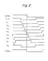
- FIG. 2shows waveforms at each portion of the phase synchronization circuit 3 in Fig. 1.
- the phase synchronization circuit 3is fundamentally composed of a delay circuit 31 and a selection circuit 32.
- the delay circuit 31produces a clock signal CLK, for instance, a dot clock signal having a frequency of 7.2 MHz, delayed in sequence to produce in sequence clock signals K 1 , K 2 , K 3 , ... , K n different in phase from each other.
- the selection circuit 32is comprised of gate circuits and the like and employs no closed loop constitution as the conventional PLL circuit. It is therefore possible to considerably shorten the pull-in time.
- the selection circuit 32selects, from among the delayed clock signals Ki , K 2 , K 3 , ... , K n , the signal which has the nearest edge timing to the edge before the trailing edge of the exterior signal such as, for instance, a horizontal synchronization signal H sync, that is to say, the delayed clock K 4 in the figure, thus outputting the same as the output clock V (SEL).
- the clockis selected in response to it.
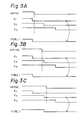
- the operation of the selection circuit 32is explained by use of the waveform diagrams in Fig. 3A to Fig. 3C. For instance, if the H sync signal falls earlier than in the case of Fig. 2, that is to say, in the case of Fig. 3A, the signal K 1 falls immediately before the signal H sync falls, so K 1 is selected. If the phase of H sync is delayed from the case of Fig. 3A, that is to say, in Fig.
- the trailing edge of K 2is nearer to the trailing edge of H sync than K i , then, as the trailing edge of K 2 is located after that of H sync, Ki is nevertheless also selected as in Fig. 3A. If the phase of H sync is further delayed, that is to say, in Fig. 3C, the trailing edge of K 2 is immediately before that of H sync, so K 2 is selected.
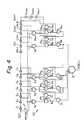
- Figure 4shows the detailed circuitry of the phase synchronization circuit of Fig. 1.
- cascade-connected inverters 1 1 , 1 2 , 1 3 , ... , I 2n+7form the delay circuit 31, while NAND gates Ai , B 1 , Ci , D 1 ; A 2 , 8 2 , C 2 , D 2 ; ... A n+1 , B n+1 , C n+1 D n+1; and E form the selection circuit 32.
- An external signalfor instance, a horizontal synchronizing signal H sync, is applied to one input of NAND gates A 1 , A 2 , A3 , ... A n+1 in the input portion of each unit, while two other inputs are connected with each inverter forming a delay circuit by shifting by two units and extending over three units.
- a pair of NAND gates in each unit B 1 , Ci; B 2 , C 2 ; ... B n+ i , C n+1form respective SR flip-flops FF 1 through FF n+1 .
- D n+1 at the output portion of each unitis connected with the output of each SR flip-flop FF(1) to FF(n+1), another input of NAND gates D 1 , D 2 , ... D n+1 is connected with the output of inverters 1 4 , 1 6 ... I 2n+4 of the delay circuit, while the output is connected with the input of the NAND gate E.
- the last unitforms a dummy circuit.
- the output of NAND gate D n+1 in this unitis not input to the NAND gate E.
- a set input of the SR flip-flops in each unitis connected with the output of the NAND gates of the input portion in the same unit, while a reset input R is connected with the output of the NAND gate of the output portion in the following unit.
- the reset input R of SR flip-flops in the last unitis connected with the output of inverters I 2n+7 in the last unit of the delay circuit.
- the last two inverters I 2n+6 and I 2n+7 in the delay circuitmay be omitted to connect the reset input R with the output of the inverter 1 2n+5.
- Figure 5illustrates the waveforms of each portion in case of a high level of the horizontal synchronizing signal H sync.
- the waveforms of the input clock signal CLK and the output of each inverter I, , 1 2 , 1 3 , I 4are delayed by the time ⁇ T of one of the inverters, for instance, 10 nsec.
- the output of the NAND gate Ais a low level only in the case of a high level of potential in both CLK and the output of 1 3 .
- the SR flip-flop FF 1composed of the NAND gates B 1 and C 1 is set at the declining time of the A 1 output signal, so the potential of the outputting point of the SR flip-flop, i.e, that of the B 1 output, is raised in response to the last transition.
- the potential of the output of the NAND gate Di in the output portioni.e., that of the D 1 output
- the potential of the output of the NAND gate Di in the output portioni.e., that of the D 1 output
- the potential of the output of the NAND gate Di in the output portioni.e., that of the D 1 output
- the potential of the output of the NAND gate Di in the output portioni.e., that of the D 1 output
- the D 2 output of the second stage of unitsfalls when it is delayed by the equivalent of two gates from the D 1 output of the first stage of units, that is to say, by the equivalent of two inverters. Accordingly, the SR flip-flop of the first stage of units is reset when the D 2 output of the second stage of units falls.
- the B 1 outputchanges to the low level and the D 1 output changes to the high level. That is to say, the signal of the D 1 output at the first stage of units becomes a pulse of negative polarity having a time duration equivalent to the delay time of two gates.
- the D 2 output of the second stage of unitsalso has a time duration equivalent to a delay time of two gates and becomes a pulse of negative polarity which falls after the D 1 output signal has been risen.
- Figure 6shows the waveforms of each portion when the horizontal synchronizing signal H sync falls, for instance, at the neighboring point of time when the output of the inverter I 2 , i.e., the 1 2 output signal, rises.
- the A 1 output signali.e., the output of the NAND gate A 1 goes high when the horizontal synchronizing signal H sync falls.
- the SR flip-flop of the first stage of unitsis set when the A 1 output signal falls, so, at that time, the B 1 output signal changes from the low level to the high level.
- the potential of D 1 output as the output of the NAND gate D 1 in the output portionchanges to the low level when the potential of I 4 output rises.
- the output of the NAND gate A 2 in the input portion of the second stage of unitsis always the high level and, as the output of the SR flip-flop FF 2 composed of the NAND gates B 2 and C 2 remains at the low level, the potential of the D 2 output, i.e., the output of the second stage of units, is held at the high level.
- the SR flip-flop of the first stage of unitsis not reset when the potential of the D 2 output is a high level, the potential of the D 1 output, i.e., the output of the first stage of units, is kept at the low level.
- Figure 7illustrates the waveforms of each portion in the vicinity of the horizontal synchronizing signal H sync.
- the outputs of each unit, D 1 output, D 2 output, and so onhave waveforms which change to a low level in sequence by a time equivalent to the delay time per two gates.
- the output V (SEL) of the NAND gate Eis a high level over nearly the whole period.
- the output V (SEL) of the NAND gate Eis a signal which is the inverted signal of the clock pulse of D 1 output, that is, a signal of clock pulse of I 4 output. It is possible to obtain the clock pulse supplied to one input terminal of the NAND gate D 1 in the output portion from a tap of the delay circuit in accordance with a desired phase.
- the clock pulse which has the nearest leading edge timing to the point of time of the trailing edge before the time when the following horizontal synchronizing signal H sync fallsis selected and the signal V (I 4 ) output is as K out .
- the delay time of the delay circuitneeds to be one period of time of the clock pulse.
- the number of gates in the plurality of inverters which constitute the delay circuitshould be selected in consideration of the extent of operation and the allowance of phase error between the external signal and the output signal.
- multi-stage invertersare employed in the delay circuit. It is not always necessary that the number of stages of multi-stage inverters be large, for instance, when applied to a CRT controller and the like. As long as the phase error creates no unnatural feature on the display screen, the number of stages of the multi-stage inverters in the delay circuit can be kept to a moderate extent and comparatively simple circuitry is sufficient.
- phase synchronizing circuit in accordance with the present inventionmay be applicable to display of channel numbers in a television display controller (TVDC) to denote the channel number and the like on the screen of a picture tube.
- TVDCtelevision display controller
Landscapes
- Synchronizing For Television (AREA)
- Stabilization Of Oscillater, Synchronisation, Frequency Synthesizers (AREA)
Description
- The present invention relates to a phase synchronization circuit. The phase synchronization circuit according to the present invention may be used for a graphic display device in a teletext receiving system.
- In a graphic display system, in general, a clock pulse is produced phase-synchronized with a synchronizing signal of a television receiver. This clock pulse is used for reading picture data from a picture memory and preparing dot signals for displaying characters, etc. for input into the television receiver. It is necessary that the phase synchronization circuit used for such a graphic display system is improved in reliability and reduced in cost through large-scale integration.
- At the same time, it is necessary that no falling out of synchronization is liable to occur and, if synchronization is lost, the pulling-in to synchronization is achieved in a short time.
- Of the prior art phase synchronization circuits, the phased-locked loop (PLL) circuit is well known. A PLL circuit includes a voltage-controlled oscillator and a comparator. In the circuit, the phase difference between the input signal and the output of the voltage-controlled oscillator is compared by the comparator to generate a voltage proportional to the phase difference. The voltage is fed back to the voltage-controlled oscillator for the phase synchronization.
- Accordingly, the PLL circuit is basically built on a feedback circuit. By enlarging the loop gain, it is possible to considerably reduce the phase difference between the input signal and the output signal.
- However, since such a PLL circuit requires use of an integrated circuit (IC) for the feedback circuit, pull-in takes a longer time. Once synchronization has been lost for some reason, there is the disadvantage that it takes a long time, for example, several milliseconds, before the PLL circuit restores the synchronization state. Moreover, the PLL circuit requires external electronic components, for instance, capacitors, making complete circuit integration difficult, thus increasing the cost of the circuit and reducing reliability.
- Another approach to the general problem of generating a signal correctly synchronized with an external signal is disclosed in patent document FR-A-2 313 827. In this prior art solution, the external signal is fed to the data input of each of a series of flip-flops clocked with a different phase relation between them. The flip-flop outputs are logically combined with the phase-shifted clock signals to extract the required synchronization signal.
- It is an object of the present invention to provide an improved phase synchronization circuit which solves the problems of the prior art.
- It is another object of the present invention to provide an improved phase synchronization circuit with an extremely short pull-in time and thus highspeed phase synchronization.
- It is a further object of the present invention to provide an improved phase synchronization circuit amenable to circuit integration and thus able to be reduced in cost and improved in reliability.
- According to the present invention as defined in
claim 1, there is provided a phase synchronization method for generating an output signal which is synchronized with a reference signal, said method comprising the step of delaying a clock signal using a delay circuit portion having a plurality of taps to produce in sequence from said plurality of taps, delayed clock signals having different phases, and selecting one of said delayed clock signals by means of a selection circuit portion including set/reset circuits and gate circuits corresponding to predetermined taps of said delay circuit portion, each of said gate circuits receiving the output of one of said set/reset circuits and one of said delayed clock signals, characterized in that said synchronization method is performed such that, when the potential of said reference signal is in one of the binary values, the set/reset operation of said set/reset circuits is carried out successively in accordance with the transmission of said clock signal through said delay circuit portion, resulting in a constant level being delivered as said output signal, while when the potential of said reference signal is changed to the other of the binary values, set/reset circuits other than the set/reset circuit which was set immediately before said change of potential are maintained in the reset state, so that the delayed clock signal of the corresponding tap of said delay circuit portion is delivered as said output signal through a gate circuit which receives the output of said set/reset circuit which was set immediately before said change of potential. - The present invention also relates to a synchronization circuit defined in
claim 4 andsubclaims 5 to 13 inclusive. - In the drawings,
- Figure 1 is a schematic diagram of a teletext receiving system with the phase synchronization circuit according to an embodiment of the present invention;
- Figures 2, 3A, 3B and 3C illustrate waveforms of the signals appearing in the system of Figure 1;
- Figure 4 shows the structure of the phase synchronization circuit in the system of Figure 1; and
- Figures 5, 6 and 7 illustrate waveforms of the signals appearing in the circuit of Figure 4.
- Figure 1 illustrates a teletext receiving system as one example of a device utilizing a
phase synchronization circuit 3 of one embodiment in accordance with the present invention. As shown in the figure, the system includes atelevision receiver 8 including a television tuner, a display unit using a cathode ray tube (CRT), and the like, and ateletext adapter 1. Theteletext adapter 1 is composed of aCRT controller 2, apicture memory 4 for storing a character code and so on, a central processor unit (CPU) 5, aprocessing memory 6 connected with theCPU 5, and adata slicer 7. - In the system as shown in Fig. 1, the picture signal SIG (VD) which is output from the television tuner contained in the
television receiver 8 is input into thedata slicer 7 in theteletext adapter 1, extracting teletext data to input it into theCPU 5. On the other hand, theCRT controller 2 is provided with aphase synchronization circuit 3 according to the embodiment of the preset invention and produces a clock signal V (SEL) phase-synchronized with a vertical synchronization signal V sync and a horizontal synchronization signal H sync, both input from thetelevision receiver 8. Based upon the teletext data, picture data is produced for storage into thepicture memory 4 through theCRT controller 2. TheCRT controller 2 reads the picture data stored in thepicture memory 4 in synchronization with the clock signal and produces a dot signal SIG (DT) for input to thetelevision receiver 8. Due to this input, characters and graphic figures are displayed on the display unit of thetelevision receiver 8 in response to the teletext data. - Figure 2 shows waveforms at each portion of the
phase synchronization circuit 3 in Fig. 1. Thephase synchronization circuit 3 is fundamentally composed of adelay circuit 31 and aselection circuit 32. Thedelay circuit 31 produces a clock signal CLK, for instance, a dot clock signal having a frequency of 7.2 MHz, delayed in sequence to produce in sequence clock signals K1, K2, K3, ... , Kn different in phase from each other. - In the phase synchronization circuit of Fig. 1, the
selection circuit 32 is comprised of gate circuits and the like and employs no closed loop constitution as the conventional PLL circuit. It is therefore possible to considerably shorten the pull-in time. As shown in Fig. 2, theselection circuit 32 selects, from among the delayed clock signals Ki , K2, K3 , ... , Kn, the signal which has the nearest edge timing to the edge before the trailing edge of the exterior signal such as, for instance, a horizontal synchronization signal H sync, that is to say, the delayed clock K4 in the figure, thus outputting the same as the output clock V (SEL). - If the phase of H sync shifts, however, then the clock is selected in response to it. The operation of the
selection circuit 32 is explained by use of the waveform diagrams in Fig. 3A to Fig. 3C. For instance, if the H sync signal falls earlier than in the case of Fig. 2, that is to say, in the case of Fig. 3A, the signal K1 falls immediately before the signal H sync falls, so K1 is selected. If the phase of H sync is delayed from the case of Fig. 3A, that is to say, in Fig. 3B, the trailing edge of K2 is nearer to the trailing edge of H sync than Ki, then, as the trailing edge of K2 is located after that of H sync, Ki is nevertheless also selected as in Fig. 3A. If the phase of H sync is further delayed, that is to say, in Fig. 3C, the trailing edge of K2 is immediately before that of H sync, so K2 is selected. - Figure 4 shows the detailed circuitry of the phase synchronization circuit of Fig. 1. In the circuit of Fig. 4, cascade-connected
inverters delay circuit 31, while NAND gates Ai , B1 , Ci , D1; A2, 82, C2, D2; ... An+1, Bn+1 , Cn+1 Dn+1; and E form theselection circuit 32. Each four NAND gates surrounded by semi- colons among these NAND gates, except E, form each unit of the selection circuit. An external signal, for instance, a horizontal synchronizing signal H sync, is applied to one input of NAND gates A1, A2, A3 , ... An+1 in the input portion of each unit, while two other inputs are connected with each inverter forming a delay circuit by shifting by two units and extending over three units. A pair of NAND gates in each unit B1, Ci; B2, C2; ... Bn+i , Cn+1 form respective SR flip-flops FF1 through FFn+1. One input of NAND gates D1, D2, ... Dn+1 at the output portion of each unit is connected with the output of each SR flip-flop FF(1) to FF(n+1), another input of NAND gates D1, D2, ... Dn+1 is connected with the output ofinverters inverter 12n+5. When the two inverters are omitted, however, the pulse width of the output of the NAND gate Dn+1 in the last unit, that is to say, the pulse width of the reset signal, is reduced, so it is necessary for each NAND gate forming the SR flip-flop of the former unit to be a high speed type. - Next, the operation of the circuit in Fig. 4 will be explained referring to the waveforms in Fig. 5 to Fig. 7. Figure 5 illustrates the waveforms of each portion in case of a high level of the horizontal synchronizing signal H sync. As is shown at the V (CLK) through V (I4) in Fig. 5, the waveforms of the input clock signal CLK and the output of each inverter I, , 12, 13, I4 are delayed by the time ΔT of one of the inverters, for instance, 10 nsec. In the circuit of the first unit, the output of the NAND gate A, is a low level only in the case of a high level of potential in both CLK and the output of 13. The SR flip-flop FF1 composed of the NAND gates B1 and C1 is set at the declining time of the A1 output signal, so the potential of the outputting point of the SR flip-flop, i.e, that of the B1 output, is raised in response to the last transition. As the potential of the output of the NAND gate Di in the output portion, i.e., that of the D1 output, is a low level when both the potentials of the B1 output and 14 output are a high level, it becomes the low level when the potential of 14 output changes from the low level to high level. In the same way, the D2 output of the second stage of units falls when it is delayed by the equivalent of two gates from the D1 output of the first stage of units, that is to say, by the equivalent of two inverters. Accordingly, the SR flip-flop of the first stage of units is reset when the D2 output of the second stage of units falls. At this time, the B1 output changes to the low level and the D1 output changes to the high level. That is to say, the signal of the D1 output at the first stage of units becomes a pulse of negative polarity having a time duration equivalent to the delay time of two gates. In the same way, the D2 output of the second stage of units also has a time duration equivalent to a delay time of two gates and becomes a pulse of negative polarity which falls after the D1 output signal has been risen.
- Figure 6 shows the waveforms of each portion when the horizontal synchronizing signal H sync falls, for instance, at the neighboring point of time when the output of the inverter I2 , i.e., the 12 output signal, rises. In this case, the A1 output signal, i.e., the output of the NAND gate A1 goes high when the horizontal synchronizing signal H sync falls. The SR flip-flop of the first stage of units is set when the A1 output signal falls, so, at that time, the B1 output signal changes from the low level to the high level. The potential of D1 output as the output of the NAND gate D1 in the output portion changes to the low level when the potential of I4 output rises. In this case, the output of the NAND gate A2 in the input portion of the second stage of units is always the high level and, as the output of the SR flip-flop FF2 composed of the NAND gates B2 and C2 remains at the low level, the potential of the D2 output, i.e., the output of the second stage of units, is held at the high level. As the SR flip-flop of the first stage of units is not reset when the potential of the D2 output is a high level, the potential of the D1 output, i.e., the output of the first stage of units, is kept at the low level.
- Figure 7 illustrates the waveforms of each portion in the vicinity of the horizontal synchronizing signal H sync. For the duration of the horizontal synchronizing signal, that is to say, the period when the horizontal synchronizing signal H sync is a high level, as is apparent from Fig. 5, the outputs of each unit, D1 output, D2 output, and so on have waveforms which change to a low level in sequence by a time equivalent to the delay time per two gates. Thus, the output V (SEL) of the NAND gate E is a high level over nearly the whole period. As shown in Fig. 6, after the fall of the horizontal synchronizing signal H sync from a high level to a low level, only one among the SR flip-flops in each unit is in a set state, while the other SR flip-flops are in a reset state. Accordingly, the potential of the output of the SR flip-flop which has been in a set state, that is to say, that of the B1 output, is a high level, while the output of all the other SR flip-flops is a low level. Thus, only one NAND gate, for instance, the NAND gate D1, of the output portion in each unit outputs a clock pulse, while the output of all the other NAND gates is a high level. As a result, while the horizontal synchronizing signal H sync is a low level, the output V (SEL) of the NAND gate E is a signal which is the inverted signal of the clock pulse of D1 output, that is, a signal of clock pulse of I4 output. It is possible to obtain the clock pulse supplied to one input terminal of the NAND gate D1 in the output portion from a tap of the delay circuit in accordance with a desired phase. In this way, during the period when the horizontal synchronizing signal H sync is a low level, after a definite phase of the clock pulse has been output from one unit, the clock pulse which has the nearest leading edge timing to the point of time of the trailing edge before the time when the following horizontal synchronizing signal H sync falls is selected and the signal V (I4 ) output is as Kout.
- From the above-described embodiment, the delay time of the delay circuit needs to be one period of time of the clock pulse. The number of gates in the plurality of inverters which constitute the delay circuit should be selected in consideration of the extent of operation and the allowance of phase error between the external signal and the output signal. According to the present invention, multi-stage inverters are employed in the delay circuit. It is not always necessary that the number of stages of multi-stage inverters be large, for instance, when applied to a CRT controller and the like. As long as the phase error creates no unnatural feature on the display screen, the number of stages of the multi-stage inverters in the delay circuit can be kept to a moderate extent and comparatively simple circuitry is sufficient. As an example, a phase error of ±20 ns or so is not a problem from the standpoint of vision. It is apparent that the phase synchronizing circuit in accordance with the present invention may be applicable to display of channel numbers in a television display controller (TVDC) to denote the channel number and the like on the screen of a picture tube.
Claims (13)
characterized in that each of said adjacent selection circuit units comprises :
Applications Claiming Priority (2)
| Application Number | Priority Date | Filing Date | Title |
|---|---|---|---|
| JP59059466AJPS60204121A (en) | 1984-03-29 | 1984-03-29 | phase locked circuit |
| JP59466/84 | 1984-03-29 |
Publications (3)
| Publication Number | Publication Date |
|---|---|
| EP0157701A2 EP0157701A2 (en) | 1985-10-09 |
| EP0157701A3 EP0157701A3 (en) | 1987-09-09 |
| EP0157701B1true EP0157701B1 (en) | 1991-12-27 |
Family
ID=13114112
Family Applications (1)
| Application Number | Title | Priority Date | Filing Date |
|---|---|---|---|
| EP85400616AExpired - LifetimeEP0157701B1 (en) | 1984-03-29 | 1985-03-29 | Phase synchronization circuit |
Country Status (4)
| Country | Link |
|---|---|
| US (1) | US4713621A (en) |
| EP (1) | EP0157701B1 (en) |
| JP (1) | JPS60204121A (en) |
| DE (1) | DE3584985D1 (en) |
Families Citing this family (61)
| Publication number | Priority date | Publication date | Assignee | Title |
|---|---|---|---|---|
| US4675612A (en)* | 1985-06-21 | 1987-06-23 | Advanced Micro Devices, Inc. | Apparatus for synchronization of a first signal with a second signal |
| CA1297171C (en)* | 1986-04-01 | 1992-03-10 | Samuel Howard Gailbreath Jr. | Digital phase lock loop |
| US4796095A (en)* | 1986-09-09 | 1989-01-03 | Rioch Company, Limited | Method of generating image scanning clock signals in optical scanning apparatus |
| US4814879A (en)* | 1987-08-07 | 1989-03-21 | Rca Licensing Corporation | Signal phase alignment circuitry |
| US4868514A (en)* | 1987-11-17 | 1989-09-19 | International Business Machines Corporation | Apparatus and method for digital compensation of oscillator drift |
| US4847870A (en)* | 1987-11-25 | 1989-07-11 | Siemens Transmission Systems, Inc. | High resolution digital phase-lock loop circuit |
| JPH01149516A (en)* | 1987-12-04 | 1989-06-12 | Mitsubishi Electric Corp | Clock generating circuit |
| JPH07114348B2 (en)* | 1987-12-11 | 1995-12-06 | 日本電気株式会社 | Logic circuit |
| US4789996A (en)* | 1988-01-28 | 1988-12-06 | Siemens Transmission Systems, Inc. | Center frequency high resolution digital phase-lock loop circuit |
| US4965815A (en)* | 1988-07-21 | 1990-10-23 | U.S. Philips Corporation | Phase detection circuit for stepwise measurement of a phase relation |
| JPH0773255B2 (en)* | 1989-03-17 | 1995-08-02 | 富士通株式会社 | Bit collation control method |
| JPH0732389B2 (en)* | 1989-09-22 | 1995-04-10 | 日本電気株式会社 | Black Jitter suppression circuit |
| US5053717A (en)* | 1989-10-05 | 1991-10-01 | Motorola, Inc. | FSK demodulator |
| US5015871A (en)* | 1989-11-03 | 1991-05-14 | Harris Corporation | Multiple external asynchronous triggers circuit |
| US5258660A (en)* | 1990-01-16 | 1993-11-02 | Cray Research, Inc. | Skew-compensated clock distribution system |
| JP2868266B2 (en)* | 1990-01-25 | 1999-03-10 | 株式会社日本自動車部品総合研究所 | Signal phase difference detection circuit and signal phase difference detection method |
| US5073730A (en)* | 1990-04-23 | 1991-12-17 | International Business Machines Corporation | Current transient reduction for vlsi chips |
| US5066868A (en)* | 1990-08-13 | 1991-11-19 | Thomson Consumer Electronics, Inc. | Apparatus for generating phase shifted clock signals |
| US5107264A (en)* | 1990-09-26 | 1992-04-21 | International Business Machines Corporation | Digital frequency multiplication and data serialization circuits |
| DE4142825A1 (en)* | 1990-12-26 | 1992-07-02 | Mitsubishi Electric Corp | SYNCHRONIZED CLOCK GENERATOR |
| US5291070A (en)* | 1991-01-28 | 1994-03-01 | Advanced Micro Devices, Inc. | Microprocessor synchronous timing system |
| JPH04298116A (en)* | 1991-03-27 | 1992-10-21 | Toshiba Corp | Sampling signal generating circuit |
| US5272390A (en)* | 1991-09-23 | 1993-12-21 | Digital Equipment Corporation | Method and apparatus for clock skew reduction through absolute delay regulation |
| US5245231A (en)* | 1991-12-30 | 1993-09-14 | Dell Usa, L.P. | Integrated delay line |
| US5534808A (en)* | 1992-01-31 | 1996-07-09 | Konica Corporation | Signal delay method, signal delay device and circuit for use in the apparatus |
| JP3381938B2 (en)* | 1992-06-05 | 2003-03-04 | 株式会社東芝 | Input transition detection pulse generation circuit |
| SE515076C2 (en)* | 1992-07-01 | 2001-06-05 | Ericsson Telefon Ab L M | Multiplexer / demultiplexer circuit |
| US5404437A (en)* | 1992-11-10 | 1995-04-04 | Sigma Designs, Inc. | Mixing of computer graphics and animation sequences |
| JP3247190B2 (en)* | 1993-04-13 | 2002-01-15 | 三菱電機株式会社 | Phase locked loop circuit and integrated circuit device |
| US5587675A (en)* | 1993-08-12 | 1996-12-24 | At&T Global Information Solutions Company | Multiclock controller |
| US5515107A (en)* | 1994-03-30 | 1996-05-07 | Sigma Designs, Incorporated | Method of encoding a stream of motion picture data |
| US5598576A (en)* | 1994-03-30 | 1997-01-28 | Sigma Designs, Incorporated | Audio output device having digital signal processor for responding to commands issued by processor by emulating designated functions according to common command interface |
| JP2830735B2 (en)* | 1994-04-19 | 1998-12-02 | 日本電気株式会社 | Phase-locked timing generator |
| JP3553639B2 (en)* | 1994-05-12 | 2004-08-11 | アジレント・テクノロジーズ・インク | Timing adjustment circuit |
| US5689530A (en)* | 1994-06-22 | 1997-11-18 | Alcatel Network Systems, Inc. | Data recovery circuit with large retime margin |
| US5592519A (en)* | 1994-06-22 | 1997-01-07 | Alcatel Network Systems, Inc. | Dual frequency clock recovery using common multitap line |
| US6124897A (en)* | 1996-09-30 | 2000-09-26 | Sigma Designs, Inc. | Method and apparatus for automatic calibration of analog video chromakey mixer |
| US5528309A (en) | 1994-06-28 | 1996-06-18 | Sigma Designs, Incorporated | Analog video chromakey mixer |
| JP3461944B2 (en)* | 1994-12-26 | 2003-10-27 | 富士通株式会社 | Pulse signal shaping circuit |
| US6239627B1 (en)* | 1995-01-03 | 2001-05-29 | Via-Cyrix, Inc. | Clock multiplier using nonoverlapping clock pulses for waveform generation |
| EP0842578A4 (en)* | 1995-08-01 | 1998-12-09 | Auravision Corp | Transition aligned video synchronization system |
| US5663767A (en)* | 1995-10-25 | 1997-09-02 | Thomson Consumer Electronics, Inc. | Clock re-timing apparatus with cascaded delay stages |
| US5945861A (en)* | 1995-12-18 | 1999-08-31 | Lg Semicon., Co. Ltd. | Clock signal modeling circuit with negative delay |
| KR0179779B1 (en)* | 1995-12-18 | 1999-04-01 | 문정환 | Clock signl modelling circuit |
| US5719511A (en)* | 1996-01-31 | 1998-02-17 | Sigma Designs, Inc. | Circuit for generating an output signal synchronized to an input signal |
| US5818468A (en)* | 1996-06-04 | 1998-10-06 | Sigma Designs, Inc. | Decoding video signals at high speed using a memory buffer |
| US6128726A (en) | 1996-06-04 | 2000-10-03 | Sigma Designs, Inc. | Accurate high speed digital signal processor |
| US5959481A (en)* | 1997-02-18 | 1999-09-28 | Rambus Inc. | Bus driver circuit including a slew rate indicator circuit having a one shot circuit |
| US6154079A (en)* | 1997-06-12 | 2000-11-28 | Lg Semicon Co., Ltd. | Negative delay circuit operable in wide band frequency |
| US6184936B1 (en) | 1997-10-06 | 2001-02-06 | Sigma Designs, Inc. | Multi-function USB capture chip using bufferless data compression |
| US6690834B1 (en) | 1999-01-22 | 2004-02-10 | Sigma Designs, Inc. | Compression of pixel data |
| US6675297B1 (en) | 1999-03-01 | 2004-01-06 | Sigma Designs, Inc. | Method and apparatus for generating and using a tamper-resistant encryption key |
| US6687770B1 (en) | 1999-03-08 | 2004-02-03 | Sigma Designs, Inc. | Controlling consumption of time-stamped information by a buffered system |
| CA2270516C (en) | 1999-04-30 | 2009-11-17 | Mosaid Technologies Incorporated | Frequency-doubling delay locked loop |
| GB2349755B (en)* | 1999-05-07 | 2003-05-14 | Synectix Ltd | Clock signal generator |
| RU2167493C1 (en)* | 2000-02-07 | 2001-05-20 | Пензенский технологический институт | Synchronizing device |
| US6654956B1 (en) | 2000-04-10 | 2003-11-25 | Sigma Designs, Inc. | Method, apparatus and computer program product for synchronizing presentation of digital video data with serving of digital video data |
| US6441666B1 (en)* | 2000-07-20 | 2002-08-27 | Silicon Graphics, Inc. | System and method for generating clock signals |
| US6704882B2 (en) | 2001-01-22 | 2004-03-09 | Mayo Foundation For Medical Education And Research | Data bit-to-clock alignment circuit with first bit capture capability |
| US7120215B2 (en)* | 2001-12-12 | 2006-10-10 | Via Technologies, Inc. | Apparatus and method for on-chip jitter measurement |
| US7680618B2 (en)* | 2007-09-28 | 2010-03-16 | Tektronix, Inc. | Random edge calibration of oversampling digital acquisition system |
Family Cites Families (11)
| Publication number | Priority date | Publication date | Assignee | Title |
|---|---|---|---|---|
| US3024417A (en)* | 1960-01-07 | 1962-03-06 | Collins Radio Co | Proportional digital synchronizer |
| FR1277331A (en)* | 1960-10-17 | 1961-12-01 | Central De Telecomm Sa Lab | Improvements to pulse regeneration devices |
| US3502991A (en)* | 1967-06-19 | 1970-03-24 | Bell Telephone Labor Inc | Signal generator with asynchronous start |
| US3624519A (en)* | 1969-11-10 | 1971-11-30 | Westinghouse Electric Corp | Tapped delay line timing circuit |
| US4061976A (en)* | 1973-04-11 | 1977-12-06 | Nippon Steel Corporation | Receivers for pulses of different widths |
| FR2313827A1 (en)* | 1975-06-02 | 1976-12-31 | Materiel Telephonique | BINARY ELEMENT SUITES TRANSMISSION SYSTEM |
| US4023110A (en)* | 1975-12-04 | 1977-05-10 | The United States Of America As Represented By The Secretary Of The Army | Pulse comparison system |
| FR2459585A1 (en)* | 1979-06-20 | 1981-01-09 | Thomson Csf | METHOD AND DEVICE FOR REFINING THE PHASE RELEASE OF A LOCAL CLOCK |
| NL183214C (en)* | 1980-01-31 | 1988-08-16 | Philips Nv | Apparatus for synchronizing the phase of a locally generated clock signal with the phase of an input signal. |
| JPS58202680A (en)* | 1982-05-21 | 1983-11-25 | Toshiba Corp | Phase synchronizing circuit |
| DE3582914D1 (en)* | 1984-10-31 | 1991-06-27 | Rca Licensing Corp | TELEVISION DISPLAY ARRANGEMENT COMPRISING A CHARACTER GENERATOR WITH A CLOCK NOT SYNCHRONIZED WITH THE LINE FREQUENCY. |
- 1984
- 1984-03-29JPJP59059466Apatent/JPS60204121A/enactivePending
- 1985
- 1985-03-28USUS06/717,198patent/US4713621A/ennot_activeExpired - Fee Related
- 1985-03-29EPEP85400616Apatent/EP0157701B1/ennot_activeExpired - Lifetime
- 1985-03-29DEDE8585400616Tpatent/DE3584985D1/ennot_activeExpired - Lifetime
Also Published As
| Publication number | Publication date |
|---|---|
| DE3584985D1 (en) | 1992-02-06 |
| JPS60204121A (en) | 1985-10-15 |
| EP0157701A2 (en) | 1985-10-09 |
| US4713621A (en) | 1987-12-15 |
| EP0157701A3 (en) | 1987-09-09 |
Similar Documents
| Publication | Publication Date | Title |
|---|---|---|
| EP0157701B1 (en) | Phase synchronization circuit | |
| US4408198A (en) | Video character generator | |
| JPH07202657A (en) | Digital delay line | |
| US4979194A (en) | Circuit for generating pulse having predetermined time period width based on trigger signal | |
| JP3278546B2 (en) | Synchronous signal generation circuit | |
| KR100214770B1 (en) | Display Synchronization Timing Signal Generation System for Video Processing | |
| JPS581785B2 (en) | cathode ray tube display device | |
| US4623925A (en) | Television receiver having character generator with non-line locked clock oscillator | |
| US4970588A (en) | Video monitoring apparatus with plural inputs | |
| US6404833B1 (en) | Digital phase synchronizing apparatus | |
| JPH02301269A (en) | Key signal delay equipment | |
| KR890004217B1 (en) | Phase synchronization circuit | |
| EP0358275A1 (en) | Pseudo line locked write clock for picture-in-picture video applications | |
| EP0416465B1 (en) | Synchronization compensating circuit for use in scanning type display circuit | |
| JPH0546134A (en) | Video display device | |
| JP3024130B2 (en) | Arbitrary phase extraction circuit | |
| KR100721805B1 (en) | Horizontal automatic frequency control circuit | |
| JP3157554B2 (en) | Semiconductor delay line device and driving method thereof | |
| JPS639785B2 (en) | ||
| JPH0421393B2 (en) | ||
| JP2642108B2 (en) | Synchronous circuit | |
| JPH0738398A (en) | Clock switching circuit | |
| KR19980016570A (en) | Horizontal synchronous separator | |
| KR910007193Y1 (en) | Display start point variable circuit of own screen | |
| JPH03263976A (en) | Synchronizing separation circuit |
Legal Events
| Date | Code | Title | Description |
|---|---|---|---|
| PUAI | Public reference made under article 153(3) epc to a published international application that has entered the european phase | Free format text:ORIGINAL CODE: 0009012 | |
| AK | Designated contracting states | Designated state(s):DE FR GB | |
| RIN1 | Information on inventor provided before grant (corrected) | Inventor name:TEMPAKU, JUNYA Inventor name:NAKAMURA, HARUHIKO | |
| PUAL | Search report despatched | Free format text:ORIGINAL CODE: 0009013 | |
| AK | Designated contracting states | Kind code of ref document:A3 Designated state(s):DE FR GB | |
| 17P | Request for examination filed | Effective date:19880122 | |
| 17Q | First examination report despatched | Effective date:19900425 | |
| GRAA | (expected) grant | Free format text:ORIGINAL CODE: 0009210 | |
| AK | Designated contracting states | Kind code of ref document:B1 Designated state(s):DE FR GB | |
| REF | Corresponds to: | Ref document number:3584985 Country of ref document:DE Date of ref document:19920206 | |
| ET | Fr: translation filed | ||
| PLBE | No opposition filed within time limit | Free format text:ORIGINAL CODE: 0009261 | |
| STAA | Information on the status of an ep patent application or granted ep patent | Free format text:STATUS: NO OPPOSITION FILED WITHIN TIME LIMIT | |
| 26N | No opposition filed | ||
| PGFP | Annual fee paid to national office [announced via postgrant information from national office to epo] | Ref country code:GB Payment date:19930105 Year of fee payment:9 | |
| PGFP | Annual fee paid to national office [announced via postgrant information from national office to epo] | Ref country code:FR Payment date:19930330 Year of fee payment:9 | |
| PGFP | Annual fee paid to national office [announced via postgrant information from national office to epo] | Ref country code:DE Payment date:19930521 Year of fee payment:9 | |
| PG25 | Lapsed in a contracting state [announced via postgrant information from national office to epo] | Ref country code:GB Effective date:19940329 | |
| GBPC | Gb: european patent ceased through non-payment of renewal fee | Effective date:19940329 | |
| PG25 | Lapsed in a contracting state [announced via postgrant information from national office to epo] | Ref country code:FR Effective date:19941130 | |
| PG25 | Lapsed in a contracting state [announced via postgrant information from national office to epo] | Ref country code:DE Effective date:19941201 | |
| REG | Reference to a national code | Ref country code:FR Ref legal event code:ST |