EP0155044A2 - Plastic pin grid array chip carrier - Google Patents
Plastic pin grid array chip carrierDownload PDFInfo
- Publication number
- EP0155044A2 EP0155044A2EP85200279AEP85200279AEP0155044A2EP 0155044 A2EP0155044 A2EP 0155044A2EP 85200279 AEP85200279 AEP 85200279AEP 85200279 AEP85200279 AEP 85200279AEP 0155044 A2EP0155044 A2EP 0155044A2
- Authority
- EP
- European Patent Office
- Prior art keywords
- package
- lead frames
- leads
- central
- carriers
- Prior art date
- Legal status (The legal status is an assumption and is not a legal conclusion. Google has not performed a legal analysis and makes no representation as to the accuracy of the status listed.)
- Withdrawn
Links
- 239000004033plasticSubstances0.000titleclaimsabstractdescription29
- 238000000034methodMethods0.000claimsabstractdescription23
- 239000000969carrierSubstances0.000claimsabstractdescription20
- 238000000465mouldingMethods0.000claimsabstractdescription17
- 239000000463materialSubstances0.000claimsdescription9
- 238000004519manufacturing processMethods0.000claimsdescription6
- 238000002347injectionMethods0.000claimsdescription4
- 239000007924injectionSubstances0.000claimsdescription4
- 238000003780insertionMethods0.000claims1
- 230000037431insertionEffects0.000claims1
- 239000000919ceramicSubstances0.000abstractdescription21
- 239000004593EpoxySubstances0.000abstractdescription7
- 239000011521glassSubstances0.000abstractdescription7
- RYGMFSIKBFXOCR-UHFFFAOYSA-NCopperChemical compound[Cu]RYGMFSIKBFXOCR-UHFFFAOYSA-N0.000abstractdescription5
- 229910052802copperInorganic materials0.000abstractdescription5
- 239000010949copperSubstances0.000abstractdescription5
- 239000002991molded plasticSubstances0.000abstractdescription4
- WFKWXMTUELFFGS-UHFFFAOYSA-NtungstenChemical compound[W]WFKWXMTUELFFGS-UHFFFAOYSA-N0.000abstractdescription2
- 229910052721tungstenInorganic materials0.000abstractdescription2
- 239000010937tungstenSubstances0.000abstractdescription2
- 238000001746injection mouldingMethods0.000description4
- 238000004806packaging method and processMethods0.000description4
- 229910000881Cu alloyInorganic materials0.000description2
- 238000003491arrayMethods0.000description2
- 238000005452bendingMethods0.000description2
- 238000005219brazingMethods0.000description2
- 230000007423decreaseEffects0.000description2
- 238000005538encapsulationMethods0.000description2
- 230000000135prohibitive effectEffects0.000description2
- 238000007789sealingMethods0.000description2
- 239000000758substrateSubstances0.000description2
- 238000003466weldingMethods0.000description2
- PNEYBMLMFCGWSK-UHFFFAOYSA-NAluminaChemical compound[O-2].[O-2].[O-2].[Al+3].[Al+3]PNEYBMLMFCGWSK-UHFFFAOYSA-N0.000description1
- UCKMPCXJQFINFW-UHFFFAOYSA-NSulphideChemical compound[S-2]UCKMPCXJQFINFW-UHFFFAOYSA-N0.000description1
- PQZSQOYXZGDGQW-UHFFFAOYSA-N[W].[Pb]Chemical compound[W].[Pb]PQZSQOYXZGDGQW-UHFFFAOYSA-N0.000description1
- 239000000853adhesiveSubstances0.000description1
- 230000001070adhesive effectEffects0.000description1
- XAGFODPZIPBFFR-UHFFFAOYSA-NaluminiumChemical compound[Al]XAGFODPZIPBFFR-UHFFFAOYSA-N0.000description1
- 229910052782aluminiumInorganic materials0.000description1
- 238000010420art techniqueMethods0.000description1
- 230000015572biosynthetic processEffects0.000description1
- POIUWJQBRNEFGX-XAMSXPGMSA-NcathelicidinChemical compoundC([C@@H](C(=O)N[C@@H](CCCNC(N)=N)C(=O)N[C@@H](CCCCN)C(=O)N[C@@H](CO)C(=O)N[C@@H](CCCCN)C(=O)N[C@@H](CCC(O)=O)C(=O)N[C@@H](CCCCN)C(=O)N[C@@H]([C@@H](C)CC)C(=O)NCC(=O)N[C@@H](CCCCN)C(=O)N[C@@H](CCC(O)=O)C(=O)N[C@@H](CC=1C=CC=CC=1)C(=O)N[C@@H](CCCCN)C(=O)N[C@@H](CCCNC(N)=N)C(=O)N[C@@H]([C@@H](C)CC)C(=O)N[C@@H](C(C)C)C(=O)N[C@@H](CCC(N)=O)C(=O)N[C@@H](CCCNC(N)=N)C(=O)N[C@@H]([C@@H](C)CC)C(=O)N[C@@H](CCCCN)C(=O)N[C@@H](CC(O)=O)C(=O)N[C@@H](CC=1C=CC=CC=1)C(=O)N[C@@H](CC(C)C)C(=O)N[C@@H](CCCNC(N)=N)C(=O)N[C@@H](CC(N)=O)C(=O)N[C@@H](CC(C)C)C(=O)N[C@@H](C(C)C)C(=O)N1[C@@H](CCC1)C(=O)N[C@@H](CCCNC(N)=N)C(=O)N[C@@H]([C@@H](C)O)C(=O)N[C@@H](CCC(O)=O)C(=O)N[C@@H](CO)C(O)=O)NC(=O)[C@H](CC=1C=CC=CC=1)NC(=O)[C@H](CC(O)=O)NC(=O)CNC(=O)[C@H](CC(C)C)NC(=O)[C@@H](N)CC(C)C)C1=CC=CC=C1POIUWJQBRNEFGX-XAMSXPGMSA-N0.000description1
- MPTQRFCYZCXJFQ-UHFFFAOYSA-Lcopper(II) chloride dihydrateChemical compoundO.O.[Cl-].[Cl-].[Cu+2]MPTQRFCYZCXJFQ-UHFFFAOYSA-L0.000description1
- 230000001934delayEffects0.000description1
- 125000003700epoxy groupChemical group0.000description1
- 238000007373indentationMethods0.000description1
- 238000012986modificationMethods0.000description1
- 230000004048modificationEffects0.000description1
- 238000010137moulding (plastic)Methods0.000description1
- 238000000059patterningMethods0.000description1
- 229920000647polyepoxidePolymers0.000description1
- 230000000284resting effectEffects0.000description1
- 229910000679solderInorganic materials0.000description1
- 238000005476solderingMethods0.000description1
Images


Classifications
- H—ELECTRICITY
- H01—ELECTRIC ELEMENTS
- H01L—SEMICONDUCTOR DEVICES NOT COVERED BY CLASS H10
- H01L21/00—Processes or apparatus adapted for the manufacture or treatment of semiconductor or solid state devices or of parts thereof
- H01L21/02—Manufacture or treatment of semiconductor devices or of parts thereof
- H01L21/04—Manufacture or treatment of semiconductor devices or of parts thereof the devices having potential barriers, e.g. a PN junction, depletion layer or carrier concentration layer
- H01L21/48—Manufacture or treatment of parts, e.g. containers, prior to assembly of the devices, using processes not provided for in a single one of the groups H01L21/18 - H01L21/326 or H10D48/04 - H10D48/07
- H01L21/4814—Conductive parts
- H01L21/4821—Flat leads, e.g. lead frames with or without insulating supports
- H01L21/4839—Assembly of a flat lead with an insulating support, e.g. for TAB
- H—ELECTRICITY
- H01—ELECTRIC ELEMENTS
- H01L—SEMICONDUCTOR DEVICES NOT COVERED BY CLASS H10
- H01L21/00—Processes or apparatus adapted for the manufacture or treatment of semiconductor or solid state devices or of parts thereof
- H01L21/02—Manufacture or treatment of semiconductor devices or of parts thereof
- H01L21/04—Manufacture or treatment of semiconductor devices or of parts thereof the devices having potential barriers, e.g. a PN junction, depletion layer or carrier concentration layer
- H01L21/48—Manufacture or treatment of parts, e.g. containers, prior to assembly of the devices, using processes not provided for in a single one of the groups H01L21/18 - H01L21/326 or H10D48/04 - H10D48/07
- H01L21/4814—Conductive parts
- H01L21/4821—Flat leads, e.g. lead frames with or without insulating supports
- H01L21/4842—Mechanical treatment, e.g. punching, cutting, deforming, cold welding
- H—ELECTRICITY
- H01—ELECTRIC ELEMENTS
- H01L—SEMICONDUCTOR DEVICES NOT COVERED BY CLASS H10
- H01L21/00—Processes or apparatus adapted for the manufacture or treatment of semiconductor or solid state devices or of parts thereof
- H01L21/02—Manufacture or treatment of semiconductor devices or of parts thereof
- H01L21/04—Manufacture or treatment of semiconductor devices or of parts thereof the devices having potential barriers, e.g. a PN junction, depletion layer or carrier concentration layer
- H01L21/50—Assembly of semiconductor devices using processes or apparatus not provided for in a single one of the groups H01L21/18 - H01L21/326 or H10D48/04 - H10D48/07 e.g. sealing of a cap to a base of a container
- H01L21/56—Encapsulations, e.g. encapsulation layers, coatings
- H01L21/565—Moulds
- H—ELECTRICITY
- H01—ELECTRIC ELEMENTS
- H01L—SEMICONDUCTOR DEVICES NOT COVERED BY CLASS H10
- H01L23/00—Details of semiconductor or other solid state devices
- H01L23/48—Arrangements for conducting electric current to or from the solid state body in operation, e.g. leads, terminal arrangements ; Selection of materials therefor
- H01L23/488—Arrangements for conducting electric current to or from the solid state body in operation, e.g. leads, terminal arrangements ; Selection of materials therefor consisting of soldered or bonded constructions
- H01L23/495—Lead-frames or other flat leads
- H01L23/49541—Geometry of the lead-frame
- H01L23/49548—Cross section geometry
- H01L23/49551—Cross section geometry characterised by bent parts
- H—ELECTRICITY
- H01—ELECTRIC ELEMENTS
- H01L—SEMICONDUCTOR DEVICES NOT COVERED BY CLASS H10
- H01L23/00—Details of semiconductor or other solid state devices
- H01L23/48—Arrangements for conducting electric current to or from the solid state body in operation, e.g. leads, terminal arrangements ; Selection of materials therefor
- H01L23/488—Arrangements for conducting electric current to or from the solid state body in operation, e.g. leads, terminal arrangements ; Selection of materials therefor consisting of soldered or bonded constructions
- H01L23/498—Leads, i.e. metallisations or lead-frames on insulating substrates, e.g. chip carriers
- H01L23/49861—Lead-frames fixed on or encapsulated in insulating substrates
- H—ELECTRICITY
- H01—ELECTRIC ELEMENTS
- H01L—SEMICONDUCTOR DEVICES NOT COVERED BY CLASS H10
- H01L2224/00—Indexing scheme for arrangements for connecting or disconnecting semiconductor or solid-state bodies and methods related thereto as covered by H01L24/00
- H01L2224/01—Means for bonding being attached to, or being formed on, the surface to be connected, e.g. chip-to-package, die-attach, "first-level" interconnects; Manufacturing methods related thereto
- H01L2224/42—Wire connectors; Manufacturing methods related thereto
- H01L2224/47—Structure, shape, material or disposition of the wire connectors after the connecting process
- H01L2224/48—Structure, shape, material or disposition of the wire connectors after the connecting process of an individual wire connector
- H01L2224/4805—Shape
- H01L2224/4809—Loop shape
- H01L2224/48091—Arched
- H—ELECTRICITY
- H01—ELECTRIC ELEMENTS
- H01L—SEMICONDUCTOR DEVICES NOT COVERED BY CLASS H10
- H01L2224/00—Indexing scheme for arrangements for connecting or disconnecting semiconductor or solid-state bodies and methods related thereto as covered by H01L24/00
- H01L2224/01—Means for bonding being attached to, or being formed on, the surface to be connected, e.g. chip-to-package, die-attach, "first-level" interconnects; Manufacturing methods related thereto
- H01L2224/42—Wire connectors; Manufacturing methods related thereto
- H01L2224/47—Structure, shape, material or disposition of the wire connectors after the connecting process
- H01L2224/49—Structure, shape, material or disposition of the wire connectors after the connecting process of a plurality of wire connectors
- H01L2224/491—Disposition
- H01L2224/4912—Layout
- H01L2224/49171—Fan-out arrangements
- H—ELECTRICITY
- H01—ELECTRIC ELEMENTS
- H01L—SEMICONDUCTOR DEVICES NOT COVERED BY CLASS H10
- H01L24/00—Arrangements for connecting or disconnecting semiconductor or solid-state bodies; Methods or apparatus related thereto
- H01L24/01—Means for bonding being attached to, or being formed on, the surface to be connected, e.g. chip-to-package, die-attach, "first-level" interconnects; Manufacturing methods related thereto
- H01L24/42—Wire connectors; Manufacturing methods related thereto
- H01L24/47—Structure, shape, material or disposition of the wire connectors after the connecting process
- H01L24/48—Structure, shape, material or disposition of the wire connectors after the connecting process of an individual wire connector
- H—ELECTRICITY
- H01—ELECTRIC ELEMENTS
- H01L—SEMICONDUCTOR DEVICES NOT COVERED BY CLASS H10
- H01L24/00—Arrangements for connecting or disconnecting semiconductor or solid-state bodies; Methods or apparatus related thereto
- H01L24/01—Means for bonding being attached to, or being formed on, the surface to be connected, e.g. chip-to-package, die-attach, "first-level" interconnects; Manufacturing methods related thereto
- H01L24/42—Wire connectors; Manufacturing methods related thereto
- H01L24/47—Structure, shape, material or disposition of the wire connectors after the connecting process
- H01L24/49—Structure, shape, material or disposition of the wire connectors after the connecting process of a plurality of wire connectors
- H—ELECTRICITY
- H01—ELECTRIC ELEMENTS
- H01L—SEMICONDUCTOR DEVICES NOT COVERED BY CLASS H10
- H01L2924/00—Indexing scheme for arrangements or methods for connecting or disconnecting semiconductor or solid-state bodies as covered by H01L24/00
- H01L2924/0001—Technical content checked by a classifier
- H01L2924/00014—Technical content checked by a classifier the subject-matter covered by the group, the symbol of which is combined with the symbol of this group, being disclosed without further technical details
- H—ELECTRICITY
- H01—ELECTRIC ELEMENTS
- H01L—SEMICONDUCTOR DEVICES NOT COVERED BY CLASS H10
- H01L2924/00—Indexing scheme for arrangements or methods for connecting or disconnecting semiconductor or solid-state bodies as covered by H01L24/00
- H01L2924/095—Indexing scheme for arrangements or methods for connecting or disconnecting semiconductor or solid-state bodies as covered by H01L24/00 with a principal constituent of the material being a combination of two or more materials provided in the groups H01L2924/013 - H01L2924/0715
- H01L2924/097—Glass-ceramics, e.g. devitrified glass
- H01L2924/09701—Low temperature co-fired ceramic [LTCC]
- H—ELECTRICITY
- H01—ELECTRIC ELEMENTS
- H01L—SEMICONDUCTOR DEVICES NOT COVERED BY CLASS H10
- H01L2924/00—Indexing scheme for arrangements or methods for connecting or disconnecting semiconductor or solid-state bodies as covered by H01L24/00
- H01L2924/10—Details of semiconductor or other solid state devices to be connected
- H01L2924/11—Device type
- H01L2924/14—Integrated circuits
- H—ELECTRICITY
- H01—ELECTRIC ELEMENTS
- H01L—SEMICONDUCTOR DEVICES NOT COVERED BY CLASS H10
- H01L2924/00—Indexing scheme for arrangements or methods for connecting or disconnecting semiconductor or solid-state bodies as covered by H01L24/00
- H01L2924/15—Details of package parts other than the semiconductor or other solid state devices to be connected
- H01L2924/151—Die mounting substrate
- H01L2924/1515—Shape
- H01L2924/15153—Shape the die mounting substrate comprising a recess for hosting the device
- H—ELECTRICITY
- H01—ELECTRIC ELEMENTS
- H01L—SEMICONDUCTOR DEVICES NOT COVERED BY CLASS H10
- H01L2924/00—Indexing scheme for arrangements or methods for connecting or disconnecting semiconductor or solid-state bodies as covered by H01L24/00
- H01L2924/15—Details of package parts other than the semiconductor or other solid state devices to be connected
- H01L2924/151—Die mounting substrate
- H01L2924/1517—Multilayer substrate
- H—ELECTRICITY
- H01—ELECTRIC ELEMENTS
- H01L—SEMICONDUCTOR DEVICES NOT COVERED BY CLASS H10
- H01L2924/00—Indexing scheme for arrangements or methods for connecting or disconnecting semiconductor or solid-state bodies as covered by H01L24/00
- H01L2924/15—Details of package parts other than the semiconductor or other solid state devices to be connected
- H01L2924/151—Die mounting substrate
- H01L2924/153—Connection portion
- H01L2924/1531—Connection portion the connection portion being formed only on the surface of the substrate opposite to the die mounting surface
- H01L2924/15312—Connection portion the connection portion being formed only on the surface of the substrate opposite to the die mounting surface being a pin array, e.g. PGA
- H—ELECTRICITY
- H01—ELECTRIC ELEMENTS
- H01L—SEMICONDUCTOR DEVICES NOT COVERED BY CLASS H10
- H01L2924/00—Indexing scheme for arrangements or methods for connecting or disconnecting semiconductor or solid-state bodies as covered by H01L24/00
- H01L2924/15—Details of package parts other than the semiconductor or other solid state devices to be connected
- H01L2924/151—Die mounting substrate
- H01L2924/153—Connection portion
- H01L2924/1532—Connection portion the connection portion being formed on the die mounting surface of the substrate
- H—ELECTRICITY
- H01—ELECTRIC ELEMENTS
- H01L—SEMICONDUCTOR DEVICES NOT COVERED BY CLASS H10
- H01L2924/00—Indexing scheme for arrangements or methods for connecting or disconnecting semiconductor or solid-state bodies as covered by H01L24/00
- H01L2924/15—Details of package parts other than the semiconductor or other solid state devices to be connected
- H01L2924/151—Die mounting substrate
- H01L2924/156—Material
- H01L2924/157—Material with a principal constituent of the material being a metal or a metalloid, e.g. boron [B], silicon [Si], germanium [Ge], arsenic [As], antimony [Sb], tellurium [Te] and polonium [Po], and alloys thereof
- H01L2924/15738—Material with a principal constituent of the material being a metal or a metalloid, e.g. boron [B], silicon [Si], germanium [Ge], arsenic [As], antimony [Sb], tellurium [Te] and polonium [Po], and alloys thereof the principal constituent melting at a temperature of greater than or equal to 950 C and less than 1550 C
- H01L2924/15747—Copper [Cu] as principal constituent
- H—ELECTRICITY
- H01—ELECTRIC ELEMENTS
- H01L—SEMICONDUCTOR DEVICES NOT COVERED BY CLASS H10
- H01L2924/00—Indexing scheme for arrangements or methods for connecting or disconnecting semiconductor or solid-state bodies as covered by H01L24/00
- H01L2924/15—Details of package parts other than the semiconductor or other solid state devices to be connected
- H01L2924/181—Encapsulation
Definitions
- Plastic dual-in-line packageshave been used extensively to house integrated circuits in which lead frames, supported by their edges, are supported in a mold cavity.
- the plasticis injected around the lead frames, with the ends of the leads extending laterally from the package.
- the packageis provided with a central cavity into which an integrated circuit (IC) is mounted.
- ICintegrated circuit
- the integrated circuitis typically wire bonded to contact pads at the ends of the traces which extend into the central cavity of the package and the package is then sealed by a cover. Thereafter, the leads are bent orthogonal to the plane of the package such that their ends define pins which extend at right angles to the package. While it is possible to have pins which completely surround the edge of this type of plastic package, it is not possible by this technique to provide an inwardly extending array of pins because the lead frames are supported by their edges during the molding process.
- VSLICsvery large scale integrated circuits
- the number of leadsbe increased and, for this purpose, it is desirable to have an array of pins which extend orthogonal to the package and which are arranged inwardly either in concentric rings or rows to provide for double or triple the numbers of pins that could be provided by bent leads at the sides of the package.
- the conventional stamped lead frame approachcannot produce high pin count arrays because the lead frame is supported in the mold cavity at its edges.
- a ceramic packagein which a first level of tungsten leads or traces is patterned onto a ceramic base, with the exterior ends of the traces providing bonding pads to which are attached orthogonal copper alloy leads which are brazed to the bonding pads to form pins.
- An interior ring or row of leadsis provided by overlying the ceramic base with another ceramic layer and patterning another layer of traces onto this layer, again with the traces having bonding pads at their ends. These ends lie inward of the outer ring of bonding pads on the first layer. Orthogonal leads are then brazed or soldered to these bonding pads to provide the pin grid array.
- glass epoxy pin grid array packageshave been provided in which printed circuit boards are substituted for the layers of the ceramic package and in which round leads are soldered to the board to provide orthogonal pins, as opposed to the brazing in the ceramic package case.
- the circuit boardshave a relatively thin two or three ounce copper trace which has been etched out of copper laminated to the glass epoxy substrate, with the thinness of the trace resulting in relatively high path resistance.
- ceramichas a high dielectric constant, which is poor for two reasons.
- Emitter coupled logic (ECL) circuits with propagation delays of less than 1 nsare now available. If all interconnections were in alumina ceramic, the delay contribution of six inches of stripline interconnection would be a prohibitive 1.6 ns. If the same interconnection is provided in epoxy glass printed wiring the delay would still be a prohibitive 1.1 ns. Thus, the savings of one-half a circuit delay can be significant to some applications.
- this particular patentrefers to a one piece plastic molded carrier for a dual-in-line integrated circuit package or module which is again a packaging means for a device that has already been mounted. Moreover, this patent also refers to a dual-in-line device and not one which has leads perpendicular to the package on all four sides. Additionally, multiple rows are not taught in this patent. It should be noted that one of the principal objects of the above patent is to provide a dual-in-line package carrier in which the integrated circuit module may be inserted and held without imposing any such pressure or stress upon the leads thereof as might damage or completely destroy the operative integrity of the module.
- an interconnection devicewhich includes a makeable and breakable interconnection between the module and the package.
- a chip carrierwhich in turn is socketed or mounted to a board so that a second interconnection device is interposed. It will also be appreciated from the above two patents that the leads for the dual-in-line package are bent after manufacture into a position normal to the mounting plane.
- the subject inventionincludes a process involving one shot molding about nested lead frames which have their ends bent orthogonal to the finally molded package prior to molding.
- the nested lead framesare supported centrally in the mold cavity, as opposed to being edge supported. This permits one shot plastic molding of the pin grid array package.
- two sets of lead framesare nested or interdigitated from square toroidal shaped central carriers which are stacked one on top of the other. Leads extend outwardly from the central carriers, with one set of leads being offset to the plane of the other set of leads so that, in one embodiment, the leads extending outwardly from the centrally supporting toruses are interdigitated in one plane.
- the leadsare bent orthogonal to their originally supported plane so as to provide an array of pins in which an inner square array of pins is provided interiorally of an outer square array of pins.
- the lead frame pinsare inserted into corresponding conical or pyramidal shaped orifices in the mold cavity such that the pins extend from the mold cavity, with the conical or pyramidal shaped orifices guiding the pins.
- the mold cavityis configured such that injected material is prevented from entering a central region which is larger than the central carriers. Thereafter the mold cavity is closed, and a one shot injection molding operation follows, using a low dielectric constant material such as plastic.
- the resultis a package in which the pins extend perpendicular to the package from pyramids or cones, with a central region of the package being devoid of plastic to provide a central cavity.
- the aforementioned toroidal carriersare centered in this cavity with portions of the leads from the carriers extending into the plastic package thus formed.
- the toroidal carriers and leadsare then cut off at the perimeter of the cavity. This leaves interdigitated bonding pads for a chip to be mounted in the central cavity, in which the bonding pads, in one embodiment, lie in one plane.
- a heat sinkis bonded to one side of the central cavity, and a die, in the form of an integrated circuit chip, is attached to the heat sink.
- the dieAfter the die is in place on the heat sink, it is wire bonded to the aforementioned pads in a conventional manner and a top cover is then sealed over the central cavity to complete the package. While plastic cannot provide for a hermetic seal, the sealing may be done in such a way that the package has a pseudohermeticity. This is accomplished through the utilization of certain epoxies and/or ultrasonic welding techniques in which plastic reflow occurs.
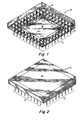
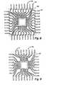
- a one shot molded plastic pin grid array 10is illustrated in which an outer ring 12 of pins surrounds an inner ring 14 of pins, with each of the pins projecting from a tapered projection 16 in the form of a pyramidal integral support structure.
- the packageis provided with a cover 18 and a rim 20 having standoffs 22 positioned thereon.
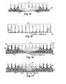
- a centrally supported lead frame stucture 30is provided with toroidally shaped central carriers 32 and 34 which are stacked one on top of the other. Leads 36 and 38 extend from each of these carriers, with leads 36 and 38 being interdigitated as shown. As can be seen, the leads from carrier 34 are offset upwardly so that the plane in which leads 36 lie is the same plane in which leads 38 lie. Ends 40 and 42 of leads 36 and 38, are bent orthogonal to the plane of the leads to provide pins. The bending occurs prior to the molding process which will be discussed hereinafter.
- leads 38are not offset from the plane of carrier 32, whereas the leads 36 are offset at 44 from carrier 34 as illustrated.
- offset 44provides that leads 36 are in the same plane as leads 38 when carrier 32 is stacked on top of carrier 34.
- the topmost lead frameis initially stamped so that it is held by an external carrier 50, whereas in Figure 7 the bottommost lead frame is originally stamped such that it is supported by an external carrier 52.
- the bottommost lead framehas exterior carrier 52 cut off and thereafter has its leads bent at the position illustrated by dotted line 56 to provide the required offset.
- the topmost lead frameis cut away from its associated carrier. Ends 40 of lead frame 36 are bent upwardly about dotted lines 58, whereas ends 42 of lead frame 38 are bent upwardly about dotted lines 60 such that upon stacking of these two lead frames, the structure of Figure 3 is achieved.
- the stacked lead frame structure 30 of Figure 3is mounted on a support 62 and over a central chamfered pilot pin or projection 63 within the bottom half 64 of the mold cavity such that lead ends 42 project into tapered or chamfered slots 66, whereas lead ends 40 project into chamfered slots 68.
- Chamfered slots 66 and 68are formed in the top half 70 of the mold cavity, with the chamfer being provided either by conical indentations or by pyramidal chamfers.
- Channels 66 and 68are provided with channel extensions 72 and 74, respectively, which accommodate ends 42 and 40, respectively, when the top half of the mold cavity is brought down over the bottom half.
- slotsmay be provided in both mold cavity halves so that pins extend from the package in opposite directions.
- the result of the one shot injection molding associated with Figure 10is a unitary package housing having a central interior aperture 80, with leads 36 and 38 having exposed ends 82 and 84 on a lip 86, with ends defining contact pads for the die to be mounted within aperture 80.
- the moldingproduces a recess 88 to one side of aperture 80 on which cover or cap 18 rests, with the outer periphery 90 of cover 18 being provided with a lip which rests on a recess 92 in the package housing.
- Heat sink 24is mounted in a recess 94 in housing 10 to an opposite side of aperture 80, with the central carrier 30 having been cut off at the periphery 98 of aperture 80 as illustrated.
- the heat sink 24is of a high thermal conductivity and may be made of copper or aluminum, with the heat sink being bonded to recess 94 by ultrasonically reflowing the plastic or using an adhesive, whereas cover 18 is made of the same type of plastic as the package and is bonded to ledge 92 by ultrasonic welding which results in plastic reflow for a pseudohermetic seaL
- a die 100is wire bonded by wires 102 to contact pads 82 and 84 as illustrated.
- the dieis mounted on heat sink 24, with package 10 then being provided with cover 18 to seal the package.
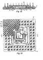
- Figure 13the wire bonding of Figure 12 can be seen from the top, with cover 18 partially removed.
- the interdigitation of the lead framescan be seen in a single plane to provide the outer square ring of the array 12 and the inner square ring of the array 14.
- Assembly 104 of Figure 14is essentially the same as that of Figure 12 with the exception that the heat sink pocket illustrated in Figure 12 no longer exists. This is a simple matter of changing the insert in the mold cavity used to produce the assembly. The reason for the removal of the heat sink pocket is so that the next level lead frame can be placed closely adjacent the first level lead frames.
- Assembly 104is characterized as having a concentric array 110 of pins which are bent up from lead frames 106 and 108 which lie at one level or plane. Each of pins 110 is captured in plastic as before.
- the lead frame 112 pins 114form an array 120 which encircles the pins associated with the first level lead frames such that increased array density is provided in a multistep process by adding to the perimeter of the device.
- the lead frames in the first levelmay be positioned closer to the center of the device such that by adding additional concentric rings the overall size of the device is not measurably increased.
- the second level lead frameis centrally supported by a central carrier 116, here in ring or torus form.
- the subsequent level lead frameshave a central carrier ring or torus which permits them to be supported from a central location, and to be positioned adjacent the already formed assembly as illustrated in Figure 16.
- an additional injection molding processproceeds such that the second level lead frame is encapsulated with plastic material 122 which bonds to the already formed plastic assembly 104 in such a manner that there is an attachment or bond between the injection molded material and the already molded plastic.
- pins 114are surrounded by tapered plastic portions 124 for the same reasons as described for the single level lead frame package. It will be seen that pin array 120 lies outside of the previously formed pin array 110.
- the assembly of Figure 16is provided with a heat sink 130 on which is mounted a die 134 which is wire bonded by wires 136 and 138 to bonding sites 140 and 142 at different levels.
- FIG. 17shows an additional ring of bond sites at a level different from that of the first ring of bond sites such that when the die is positioned on the heat sink, the contact pads on the die are wire bonded not only to the bond sites at the first level but also are wire bonded to the bond sites at the second level
- the plastic normally utilizedwhich has a low dielectric constant is polyphenelene sulfide, having a dielectric constant of 4.0, as opposed to ceramic dielectric constants of 6.5-10.0.
- the lead framesare made of copper, in which the thickness of the copper is .006 in., not only is the path resistance low, but the interlead resistance is high due to the pyramidal supports for the pins which increases the electrical path length from one exposed pin to the other.
- the low dielectric constant of the encapsulating materialminimizes cross-talk.
- the subject inventionis not limited by the number of rings utilized.
- one of the important features of the subject inventionis the central carrier which permits pin grid arrays to be fabricated in a one shot molding process, since the lead frames with bent pin ends are supported centrally from a carrier which is later removed. This provides an array in which the pins are bent prior to encapsulation.
- the subject methodalleviates the problems of solder bonding or brazing PM 2 22 84 pins to contact pads to provide a pin grid array and is both simple and economical.
Landscapes
- Engineering & Computer Science (AREA)
- Physics & Mathematics (AREA)
- Condensed Matter Physics & Semiconductors (AREA)
- General Physics & Mathematics (AREA)
- Computer Hardware Design (AREA)
- Microelectronics & Electronic Packaging (AREA)
- Power Engineering (AREA)
- Manufacturing & Machinery (AREA)
- Geometry (AREA)
- Lead Frames For Integrated Circuits (AREA)
- Encapsulation Of And Coatings For Semiconductor Or Solid State Devices (AREA)
- Structures Or Materials For Encapsulating Or Coating Semiconductor Devices Or Solid State Devices (AREA)
Abstract
Description
- Plastic dual-in-line packages (DIPs) have been used extensively to house integrated circuits in which lead frames, supported by their edges, are supported in a mold cavity. The plastic is injected around the lead frames, with the ends of the leads extending laterally from the package. The package is provided with a central cavity into which an integrated circuit (IC) is mounted. The integrated circuit is typically wire bonded to contact pads at the ends of the traces which extend into the central cavity of the package and the package is then sealed by a cover. Thereafter, the leads are bent orthogonal to the plane of the package such that their ends define pins which extend at right angles to the package. While it is possible to have pins which completely surround the edge of this type of plastic package, it is not possible by this technique to provide an inwardly extending array of pins because the lead frames are supported by their edges during the molding process.
- For very large scale integrated circuits (VSLICs) it is important that the number of leads be increased and, for this purpose, it is desirable to have an array of pins which extend orthogonal to the package and which are arranged inwardly either in concentric rings or rows to provide for double or triple the numbers of pins that could be provided by bent leads at the sides of the package. Thus, the conventional stamped lead frame approach cannot produce high pin count arrays because the lead frame is supported in the mold cavity at its edges.
- In the past, in order to provide a pin grid array chip carrier, a ceramic package is provided in which a first level of tungsten leads or traces is patterned onto a ceramic base, with the exterior ends of the traces providing bonding pads to which are attached orthogonal copper alloy leads which are brazed to the bonding pads to form pins. An interior ring or row of leads is provided by overlying the ceramic base with another ceramic layer and patterning another layer of traces onto this layer, again with the traces having bonding pads at their ends. These ends lie inward of the outer ring of bonding pads on the first layer. Orthogonal leads are then brazed or soldered to these bonding pads to provide the pin grid array. What will be appreciated is that not only are the pins not formed by a simple bending process, but also there is a multilayer trace pattern in the ceramic package which is undesirable from the point of view that the bonding pads provided for the wire bonding of the chip are at different levels within the package. Moreover the brazed joint has an unpredictable path resistance which is undesirable.
- By way of further background, glass epoxy pin grid array packages have been provided in which printed circuit boards are substituted for the layers of the ceramic package and in which round leads are soldered to the board to provide orthogonal pins, as opposed to the brazing in the ceramic package case. It should be noted in the glass epoxy version of the pin grid array chip carrier the circuit boards have a relatively thin two or three ounce copper trace which has been etched out of copper laminated to the glass epoxy substrate, with the thinness of the trace resulting in relatively high path resistance. Moreover, it should be noted that there is no lead frame in either the glass epoxy or ceramic versions.
- It will be appreciated that what is desired is not a conventional dual-in-line package which has two rows of leads projecting from it at right angles to the plane of mounting to the chip, but rather what is desired is a pin grid array which can have as many as four or more concentric rings of pins.
- The basic disadvantage to ceramic packaging is that it is expensive and that there are limitations in the control of tolerances because as larger packages are provided they are more and more difficult to fabricate. Also what occurs when providing ceramic packages is that with more and more pins, one cannot achieve a narrow enough tungsten lead without the path resistance becoming so great that the integrated circuit will not function in the ceramic package provided, thus necessitating multiple layers.
- Also, ceramic has a high dielectric constant, which is poor for two reasons. First, when using ceramic it becomes important to minimize the interconnection path length in the high dielectric constant media where the delay difference between it and a lower dielectric constant material can be a significant part of the delay in the circuit element. Emitter coupled logic (ECL) circuits with propagation delays of less than 1 ns are now available. If all interconnections were in alumina ceramic, the delay contribution of six inches of stripline interconnection would be a prohibitive 1.6 ns. If the same interconnection is provided in epoxy glass printed wiring the delay would still be a prohibitive 1.1 ns. Thus, the savings of one-half a circuit delay can be significant to some applications.
- Secondly, due to the high dielectric constant of ceramic, the interlead capacitance is high, which results in low speed operation and considerable cross-talk problems.
- From the manufacturing point of view, with respect to the conventional injection molding of dual-in-line packages, it will be appreciated that the leads are supported from opposing sides prior to molding. After the package has been molded the leads are bent down perpendicular to the package. However, in a pin grid array, more than two rows of pins or an inner ring of pins is required, which means that lead frames cannot be provided in the flat prior to the molding because the pins would be laying over one another.
- In the prior art there are a number of techniques utilized to interconnect an integrated circuit that is already packaged. As such, the total package includes an intermediate connector which is used with an already packaged integrated circuit. These packaging techniques are cumbersome and expensive, and are used to adapt an already packaged die to a particular pin configuration. One prior art technique is illustrated in U. S. Patent No. 3,789,341 in which a plastic frame is used to encapsulate the leads. It will be appreciated that in this patent leads are bonded to a carrier to which the chip has already been attached and wire bonded. Here the integrated circuit is already bonded to a substrate and the interconnection means is thereafter provided. It will also be appreciated that the device in this patent is a dual-in-line device in which the leads do not come out on all four sides of the package.
- With reference to U. S. Patent No. 3,892,312, this particular patent refers to a one piece plastic molded carrier for a dual-in-line integrated circuit package or module which is again a packaging means for a device that has already been mounted. Moreover, this patent also refers to a dual-in-line device and not one which has leads perpendicular to the package on all four sides. Additionally, multiple rows are not taught in this patent. It should be noted that one of the principal objects of the above patent is to provide a dual-in-line package carrier in which the integrated circuit module may be inserted and held without imposing any such pressure or stress upon the leads thereof as might damage or completely destroy the operative integrity of the module. This means that an interconnection device is provided which includes a makeable and breakable interconnection between the module and the package. In essence, what is provided in this patent is a chip carrier which in turn is socketed or mounted to a board so that a second interconnection device is interposed. It will also be appreciated from the above two patents that the leads for the dual-in-line package are bent after manufacture into a position normal to the mounting plane.
- Reference is also made to U. S. Patent No. 4,195,193, in which the package described refers to a plastic chip carrier. Again in this patent the leads are bent in a position normal to the seating plane after the molding of the package. Additionally, only one layer and one row can be provided around the perimeter of the package due to the fact that the leads all exit the package at the side. While there are leads on all four sides, only one ring of pins can be provided. It will be appreciated that the package of this patent is intended to be a surface mount package, which is to say that the leads are not left at right angles to the package but rather are curled around so that they can be attached directly to the surface of the board. This precludes the use of this package where pins are required to project into plated thru-holes in a printed circuit board or to pass into a conventional IC socket. In leadless surface mount packaging, pads must be placed around the perimeter of the package which means that as the package pin count increases, the leadless package must increase in circumference to accommodate the increase in leads. This is in contradistinction to the pin grid array package which requires holes in a circuit board to which it is soldered. However, the major distinction is that in a pin grid package the rows can be increased in a pin grid array moving inwardly from the periphery of the package so that more input-output (IO) terminals or leads can be provided for a smaller surface area. Another problem with surface mount devices is the differential in thermal coefficient of expansion between the surface mounted package and the board. Because of the direct soldering of the contact pad to pads on the printed circuit board, considerable stress on these joints can result.
- Other patents relating to lead frames and plastic encapsulation include U. S. Patents Nos. 3,391,382, 3,652,974, 3,678,385, 3,930,115, 3,963,315, 4,026,412, 4,144,648, 4,252,864, 4,329,642, 4,358,173, and 4,387,388. In all of these additional patents their fabrication presumes lead frames which are edge supported as opposed to the center supported method of manufacture described hereinafter.
- In contradistinction to the edge supported lead frames of the prior art, the subject invention includes a process involving one shot molding about nested lead frames which have their ends bent orthogonal to the finally molded package prior to molding. In the subject system, the nested lead frames are supported centrally in the mold cavity, as opposed to being edge supported. This permits one shot plastic molding of the pin grid array package. In one embodiment, two sets of lead frames are nested or interdigitated from square toroidal shaped central carriers which are stacked one on top of the other. Leads extend outwardly from the central carriers, with one set of leads being offset to the plane of the other set of leads so that, in one embodiment, the leads extending outwardly from the centrally supporting toruses are interdigitated in one plane. Thereafter the ends of all of the leads are bent orthogonal to their originally supported plane so as to provide an array of pins in which an inner square array of pins is provided interiorally of an outer square array of pins. Having formed such a nested centrally supported lead frame arrangement, the lead frame pins are inserted into corresponding conical or pyramidal shaped orifices in the mold cavity such that the pins extend from the mold cavity, with the conical or pyramidal shaped orifices guiding the pins. The mold cavity is configured such that injected material is prevented from entering a central region which is larger than the central carriers. Thereafter the mold cavity is closed, and a one shot injection molding operation follows, using a low dielectric constant material such as plastic. The result is a package in which the pins extend perpendicular to the package from pyramids or cones, with a central region of the package being devoid of plastic to provide a central cavity. After molding, the aforementioned toroidal carriers are centered in this cavity with portions of the leads from the carriers extending into the plastic package thus formed. The toroidal carriers and leads are then cut off at the perimeter of the cavity. This leaves interdigitated bonding pads for a chip to be mounted in the central cavity, in which the bonding pads, in one embodiment, lie in one plane. Thereafter a heat sink is bonded to one side of the central cavity, and a die, in the form of an integrated circuit chip, is attached to the heat sink. After the die is in place on the heat sink, it is wire bonded to the aforementioned pads in a conventional manner and a top cover is then sealed over the central cavity to complete the package. While plastic cannot provide for a hermetic seal, the sealing may be done in such a way that the package has a pseudohermeticity. This is accomplished through the utilization of certain epoxies and/or ultrasonic welding techniques in which plastic reflow occurs.
- Not only is a pin grid array chip carrier produced in a one shot process but also the path resistance for the relatively thick copper alloy leads is dramatically reduced over the relatively thin patterned leads for the ceramic and glass packages. Moreover, the resistance paths between leads is increased due to the conical or pyramid type structures which support the pins to reduce cross-talk. The use of the low dielectric constant plastic reduces the delay to less than one nanosecond and also decreases cross-talk, which has been so severe with ceramic systems that grounded interdigitated leads have been used to decrease cross-talk in the prior art ceramic packages.
- These and other features of the subject invention will be better understood in connection with the detailed description taken in conjunction with the drawings of which:
- Figure 1 is a perspective view of the bottom of the subject molded plastic pin grid array chip carrier package with a cap or cover in place;
- Figure 2 is a perspective view of the top of the package of Figure 1 showing the heat sink sealed to the package;
- Figure 3 is a diagrammatic illustration of the interdigitated, centrally supported lead frames showing the central toroidally-shaped, stacked carriers and the bent leads which form the pins of the subject pin grid array;
- Figure 4 is a diagrammatic illustration of portions of the two sets of lead frames prior to the stacking thereof;
- Figure 5 is a diagrammatic illustration of the stacking of the portions of the lead frames of Figure 4, illustrating the offset of the lead frames for the underneath carrier;
- Figure 6 is a top view of the stamping utilized for the fabrication of the topmost of the lead frames of Figure 3;
- Figure 7 is a top view of the stamping for the lead frames for the bottommost of the lead frames of the Figure 3;
- Figure 8 is a top view of the lead frame of Figure 7, with the external carrier removed;
- Figure 9 is a top view of the lead frame of Figure 6 with the external carrier removed;
- Figure 10 is a cross-sectional and diagrammatic illustration of the mounting of the stacked lead frames in a mold cavity over a central pilot pin or projection, illustrating the tapered channels in the cavity to receive the pins from the lead frames;
- Figure 11 is an exploded and diagrammatic view of the package produced by the molding operation of Figure 10, illustrating the position of a heat sink, the cut-off central carrier and the cover with respect to the one shot molded article;
- Figure 12 is a cross-sectional and diagrammatic view of a portion of the package of Figure 11 showing a die resting on the heat sink, with the die being wire bonded to contact pads at the ends of the leads of the lead frames in the package;
- Figure 13 is a partial sectional view of the package of Figure 12 taken from the bottom of the package, illustrating the wire bonding of the die to contact pads at the ends of various lead frames as well as the interdigitated lead frame structure;
- Figure 14 is a cross-sectional and diagrammatic view of an assembly to be provided with an additional level of lead frames;
- Figure 15 is a diagrammatic view of the additional lead frame for use with the assembly of Figure 14;
- Figure 16 is a cross-sectional and diagrammatic view of a multilevel lead frame pin grid array package absent heat sink and die; and
- Figure 17 is a cross-sectional and diagrammatic view of the multilevel package of Figure 16 showing multilevel wire bonding.
- Referring to Figure 1, in one embodiment a one shot molded plastic
pin grid array 10 is illustrated in which anouter ring 12 of pins surrounds aninner ring 14 of pins, with each of the pins projecting from a taperedprojection 16 in the form of a pyramidal integral support structure. The package is provided with acover 18 and arim 20 havingstandoffs 22 positioned thereon. - Referring to Figure 2, the package of Figure 1 is shown inverted, with the top of the package having an inlaid
heat sink 24 secured to the package. - In order to provide the pin grid array of Figure 1, and referring now to Figure 3, in one embodiment, prior to molding, a centrally supported lead frame stucture 30 is provided with toroidally shaped
central carriers leads carrier 34 are offset upwardly so that the plane in which leads 36 lie is the same plane in which leads 38 lie. Ends 40 and 42 ofleads - Referring to Figure 4, portions of the lead frames of Figure 3 are shown prior to stacking in which leads 38 are not offset from the plane of
carrier 32, whereas theleads 36 are offset at 44 fromcarrier 34 as illustrated. - Referring to Figure 5, offset 44 provides that leads 36 are in the same plane as leads 38 when
carrier 32 is stacked on top ofcarrier 34. - Referring to Figure 6, the topmost lead frame is initially stamped so that it is held by an
external carrier 50, whereas in Figure 7 the bottommost lead frame is originally stamped such that it is supported by anexternal carrier 52. - Referring to Figure 8, the bottommost lead frame has
exterior carrier 52 cut off and thereafter has its leads bent at the position illustrated by dottedline 56 to provide the required offset. - Referring to Figure 9, the topmost lead frame is cut away from its associated carrier. Ends 40 of
lead frame 36 are bent upwardly aboutdotted lines 58, whereas ends 42 oflead frame 38 are bent upwardly aboutdotted lines 60 such that upon stacking of these two lead frames, the structure of Figure 3 is achieved. - Referring now to Figure 10, the stacked
lead frame structure 30 of Figure 3 is mounted on asupport 62 and over a central chamfered pilot pin or projection 63 within thebottom half 64 of the mold cavity such that lead ends 42 project into tapered or chamferedslots 66, whereas lead ends 40 project into chamferedslots 68.Chamfered slots top half 70 of the mold cavity, with the chamfer being provided either by conical indentations or by pyramidal chamfers.Channels channel extensions - Referring to Figure 11, the result of the one shot injection molding associated with Figure 10 is a unitary package housing having a central
interior aperture 80, withleads lip 86, with ends defining contact pads for the die to be mounted withinaperture 80. The molding produces arecess 88 to one side ofaperture 80 on which cover orcap 18 rests, with theouter periphery 90 ofcover 18 being provided with a lip which rests on arecess 92 in the package housing.Heat sink 24 is mounted in arecess 94 inhousing 10 to an opposite side ofaperture 80, with thecentral carrier 30 having been cut off at theperiphery 98 ofaperture 80 as illustrated. - The
heat sink 24 is of a high thermal conductivity and may be made of copper or aluminum, with the heat sink being bonded to recess 94 by ultrasonically reflowing the plastic or using an adhesive, whereascover 18 is made of the same type of plastic as the package and is bonded toledge 92 by ultrasonic welding which results in plastic reflow for a pseudohermetic seaL - Thereafter, as illustrated in Figure 12, a
die 100 is wire bonded bywires 102 to contactpads heat sink 24, withpackage 10 then being provided withcover 18 to seal the package. - Referring to Figure 13, the wire bonding of Figure 12 can be seen from the top, with
cover 18 partially removed. Here the interdigitation of the lead frames can be seen in a single plane to provide the outer square ring of thearray 12 and the inner square ring of thearray 14. - While what has been illustrated is a single plane for the lead frames within the package which provides an array with two concentric rings of pins, it will be appreciated that additional concentric rings of pins can be provided by multiple levels of lead frames and a multistep process. This process begins with the formation of the assembly illustrated in Figure 12, absent the die, wire bonding and sealing. This assembly is illustrated in Figure 14.
Assembly 104 of Figure 14 is essentially the same as that of Figure 12 with the exception that the heat sink pocket illustrated in Figure 12 no longer exists. This is a simple matter of changing the insert in the mold cavity used to produce the assembly. The reason for the removal of the heat sink pocket is so that the next level lead frame can be placed closely adjacent the first level lead frames.Assembly 104 is characterized as having aconcentric array 110 of pins which are bent up fromlead frames pins 110 is captured in plastic as before.- Referring now to Figure 15, it will be appreciated that the
lead frame 112pins 114 form anarray 120 which encircles the pins associated with the first level lead frames such that increased array density is provided in a multistep process by adding to the perimeter of the device. Alternatively, the lead frames in the first level may be positioned closer to the center of the device such that by adding additional concentric rings the overall size of the device is not measurably increased. Again as before, the second level lead frame is centrally supported by acentral carrier 116, here in ring or torus form. It will be appreciated that the subsequent level lead frames have a central carrier ring or torus which permits them to be supported from a central location, and to be positioned adjacent the already formed assembly as illustrated in Figure 16. Once the additional lead frame is positioned adjacent the already formed structure of Figure 14 in a mold cavity, an additional injection molding process proceeds such that the second level lead frame is encapsulated withplastic material 122 which bonds to the already formedplastic assembly 104 in such a manner that there is an attachment or bond between the injection molded material and the already molded plastic. Here pins 114 are surrounded by taperedplastic portions 124 for the same reasons as described for the single level lead frame package. It will be seen thatpin array 120 lies outside of the previously formedpin array 110. - Referring to Figure 17, the assembly of Figure 16 is provided with a
heat sink 130 on which is mounted adie 134 which is wire bonded bywires bonding sites - As can be seen a further circumferential ring of pins is provided, thereby increasing the pin density of the array of Figure 14. The structure of Figure 17 also shows an additional ring of bond sites at a level different from that of the first ring of bond sites such that when the die is positioned on the heat sink, the contact pads on the die are wire bonded not only to the bond sites at the first level but also are wire bonded to the bond sites at the second level
- It will be appreciated that the plastic normally utilized, which has a low dielectric constant is polyphenelene sulfide, having a dielectric constant of 4.0, as opposed to ceramic dielectric constants of 6.5-10.0. Since, in one embodiment, the lead frames are made of copper, in which the thickness of the copper is .006 in., not only is the path resistance low, but the interlead resistance is high due to the pyramidal supports for the pins which increases the electrical path length from one exposed pin to the other. The low dielectric constant of the encapsulating material minimizes cross-talk.
- It will be appreciated that more than two concentric rings of pins can be provided for the pin grid array, such that the subject invention is not limited by the number of rings utilized. Moreover, one of the important features of the subject invention is the central carrier which permits pin grid arrays to be fabricated in a one shot molding process, since the lead frames with bent pin ends are supported centrally from a carrier which is later removed. This provides an array in which the pins are bent prior to encapsulation. The subject method alleviates the problems of solder bonding or brazing PM 2 22 84 pins to contact pads to provide a pin grid array and is both simple and economical.
- Having above indicated a preferred embodiment of the present invention, it will occur to those skilled in the art that modifications and alternatives can be practiced within the spirit of the invention. It is accordingly intended to define the scope of the invention only as indicated in the following claims.
Claims (17)
1. A plastic pin grid array package for electronic circuits in which concentric patterns of pins project normal to the bottom surface of the package.
2. The package of claim 1 wherein the package is made in a one shot molding process.
3. The package of claim 2 wherein said package is formed by the insertion of centrally supported lead frames into a mold cavity.
4. The package of claim 3 wherein said centrally supported lead frames are each supported by toroidal carriers prior to molding, said carriers being removed after molding.
5. The package of claim 3 wherein said centrally supported lead frames are each supported by carriers and wherein said carriers are stacked one on top of the other in said mold cavity, said carriers being removed after molding.
6. The package of claim 5 wherein the leads of one carrier are offset to the plane of the leads of another carrier.
7. The package of claim 3 wherein the leads of said lead frames are interdigitated in said package.
8. The package of claim 1 wherein the pins of said pin grid array are surrounded by tapered projections of plastic.
9. The package of claim 1 wherein the package includes a central aperture, a heat sink to one side of said aperture, a die on said heat sink, said die having contact pads electrically connected to said pins, and a cover to an opposing side of said aperture.
10. The package of claim 9 wherein said cover is plastic and is ultrasonically bonded to said package.
11. A method of making pin grid array electronic component packages comprising the steps of:
providing a mold cavity having cooperating mold halves with pin receiving apertures to accommodate the ends of lead frames corresponding to the pins,
locating lead frames supported by central carriers in the mold cavity, each lead frame having leads which have ends perpendicular to the corresponding lead, with the central carriers stacked one on top of the other in the mold cavity such that the lead frame ends project through corresponding pin receiving apertures, said mold cavity being configured to prevent injection molded material from entering a central region at which the central carriers are located, thereby to leave a central aperture in the part to be molded;
injecting a low dielectric constant material into the mold cavity;
removing the injection molded part;
removing the central carriers from the central aperture;
affixing a support to one side of the central aperture;
mounting an electronic component on the support, said component having contact pads;
electrically connecting the electronic component contact pads to different lead frame leads; and
mounting a cover to the opposing side of the central aperture.
12. The method of claim 11 wherein said pin receiving apertures are tapered.
13. The method of claim 11 wherein the ends of the lead frames define a concentric array of pins.
14. The method of claim 11 wherein said support is highly thermally conductive so as to form a heat sink.
15. The method of claim 11 wherein said cover and said injected material is plastic.
16. The method of claim 15 wherein said cover is bonded to the injection molded part by plastic reflow.
5 17. The method of claim 11 wherein said central carriers each have an aperture and wherein one half of said mold cavity has a projection which passes through the carrier apertures to locate said lead frames within said mold cavity.
Applications Claiming Priority (2)
| Application Number | Priority Date | Filing Date | Title |
|---|---|---|---|
| US06/585,010US4677526A (en) | 1984-03-01 | 1984-03-01 | Plastic pin grid array chip carrier |
| US585010 | 1984-03-01 |
Publications (2)
| Publication Number | Publication Date |
|---|---|
| EP0155044A2true EP0155044A2 (en) | 1985-09-18 |
| EP0155044A3 EP0155044A3 (en) | 1986-12-10 |
Family
ID=24339700
Family Applications (1)
| Application Number | Title | Priority Date | Filing Date |
|---|---|---|---|
| EP85200279AWithdrawnEP0155044A3 (en) | 1984-03-01 | 1985-02-28 | Plastic pin grid array chip carrier |
Country Status (4)
| Country | Link |
|---|---|
| US (1) | US4677526A (en) |
| EP (1) | EP0155044A3 (en) |
| JP (1) | JPS60227457A (en) |
| CA (1) | CA1229933A (en) |
Cited By (13)
| Publication number | Priority date | Publication date | Assignee | Title |
|---|---|---|---|---|
| EP0228869A3 (en)* | 1986-01-06 | 1987-09-16 | American Telephone And Telegraph Company | Electronic component package |
| EP0232837A3 (en)* | 1986-02-14 | 1989-02-22 | Matsushita Electric Industrial Co., Ltd. | Plastic molded chip carrier package and method of fabricating the same |
| EP0223234A3 (en)* | 1985-11-20 | 1989-05-10 | AMP-AKZO CORPORATION (a Delaware corp.) | Interconnection package suitable for electronic devices and methods for producing same |
| FR2631166A1 (en)* | 1988-05-09 | 1989-11-10 | Nat Semiconductor Corp | POWER BOX OF THE TYPE OF PIG GRID FOR AN INTEGRATED CIRCUIT |
| EP0382714A4 (en)* | 1987-02-19 | 1990-06-05 | Olin Corp | Process for manufacturing plastic pin grid arrays and the product produced thereby. |
| FR2647958A1 (en)* | 1989-05-30 | 1990-12-07 | Thomson Composants Militaires | Plastic housing for integrated circuit with staggered grids on two levels and method of manufacture |
| US5144412A (en)* | 1987-02-19 | 1992-09-01 | Olin Corporation | Process for manufacturing plastic pin grid arrays and the product produced thereby |
| WO1995024733A1 (en)* | 1994-03-11 | 1995-09-14 | The Panda Project | Prefabricated semiconductor chip carrier |
| US5821457A (en)* | 1994-03-11 | 1998-10-13 | The Panda Project | Semiconductor die carrier having a dielectric epoxy between adjacent leads |
| US5824950A (en)* | 1994-03-11 | 1998-10-20 | The Panda Project | Low profile semiconductor die carrier |
| US6078102A (en)* | 1998-03-03 | 2000-06-20 | Silicon Bandwidth, Inc. | Semiconductor die package for mounting in horizontal and upright configurations |
| US6141869A (en)* | 1998-10-26 | 2000-11-07 | Silicon Bandwidth, Inc. | Apparatus for and method of manufacturing a semiconductor die carrier |
| US6307258B1 (en) | 1998-12-22 | 2001-10-23 | Silicon Bandwidth, Inc. | Open-cavity semiconductor die package |
Families Citing this family (65)
| Publication number | Priority date | Publication date | Assignee | Title |
|---|---|---|---|---|
| JPS62189742A (en)* | 1986-02-14 | 1987-08-19 | Matsushita Electric Works Ltd | Pin grid array |
| JPS62189743A (en)* | 1986-02-14 | 1987-08-19 | Matsushita Electric Works Ltd | Wiring circuit unit |
| US4816426A (en)* | 1987-02-19 | 1989-03-28 | Olin Corporation | Process for manufacturing plastic pin grid arrays and the product produced thereby |
| US4965227A (en)* | 1987-05-21 | 1990-10-23 | Olin Corporation | Process for manufacturing plastic pin grid arrays and the product produced thereby |
| USD316848S (en) | 1987-07-04 | 1991-05-14 | Terutomi Hasegawa | Mounting substrate for semiconductors |
| USD317300S (en) | 1987-07-04 | 1991-06-04 | Terutomi Hasegawa | Semi-conductor mounting substrate |
| USD318271S (en) | 1987-07-04 | 1991-07-16 | Terutomi Hasegawa | Substrate for mounting semiconductors |
| GB2209867B (en)* | 1987-09-16 | 1990-12-19 | Advanced Semiconductor Package | Method of forming an integrated circuit chip carrier |
| US5168432A (en)* | 1987-11-17 | 1992-12-01 | Advanced Interconnections Corporation | Adapter for connection of an integrated circuit package to a circuit board |
| US5184285A (en)* | 1987-11-17 | 1993-02-02 | Advanced Interconnections Corporation | Socket constructed with molded-in lead frame providing means for installing additional component such as a chip capacitor |
| US5438481A (en)* | 1987-11-17 | 1995-08-01 | Advanced Interconnections Corporation | Molded-in lead frames |
| US5152057A (en)* | 1987-11-17 | 1992-10-06 | Mold-Pac Corporation | Molded integrated circuit package |
| USD319629S (en) | 1988-04-13 | 1991-09-03 | Ibiden Co., Ltd. | Semiconductor substrate with conducting pattern |
| USD318461S (en) | 1988-04-13 | 1991-07-23 | Ibiden Co., Ltd. | Semi-conductor mounting substrate |
| USD319814S (en) | 1988-04-13 | 1991-09-10 | Ibiden Co., Ltd. | Semi-conductor substrate with conducting pattern |
| EP0347238B1 (en)* | 1988-06-17 | 1993-10-20 | Ngk Insulators, Ltd. | Minutely patterned structure, and method of producing the same |
| US5046971A (en)* | 1988-12-14 | 1991-09-10 | Olin Corporation | Terminal pins for flexible circuits |
| US5057903A (en)* | 1989-07-17 | 1991-10-15 | Microelectronics And Computer Technology Corporation | Thermal heat sink encapsulated integrated circuit |
| KR100192871B1 (en)* | 1989-09-28 | 1999-06-15 | 기타지마 요시도시 | Semiconductor device having a leadframe and metal substrate |
| US5012386A (en)* | 1989-10-27 | 1991-04-30 | Motorola, Inc. | High performance overmolded electronic package |
| US4943846A (en)* | 1989-11-09 | 1990-07-24 | Amp Incorporated | Pin grid array having seperate posts and socket contacts |
| AU6966391A (en)* | 1989-11-22 | 1991-06-13 | Tactical Fabs, Inc. | High density multichip package |
| US5182632A (en)* | 1989-11-22 | 1993-01-26 | Tactical Fabs, Inc. | High density multichip package with interconnect structure and heatsink |
| US5159750A (en)* | 1989-12-20 | 1992-11-03 | National Semiconductor Corporation | Method of connecting an IC component with another electrical component |
| US5008734A (en)* | 1989-12-20 | 1991-04-16 | National Semiconductor Corporation | Stadium-stepped package for an integrated circuit with air dielectric |
| US5147815A (en)* | 1990-05-14 | 1992-09-15 | Motorola, Inc. | Method for fabricating a multichip semiconductor device having two interdigitated leadframes |
| IT220657Z2 (en)* | 1990-10-30 | 1993-10-08 | Marelli Autronica | ELECTRONIC DEVICE INCLUDING AN INTEGRATED CIRCUIT MOUNTED ON AN INSULATING BASE. |
| JP2872825B2 (en)* | 1991-05-13 | 1999-03-24 | 三菱電機株式会社 | Package for semiconductor device |
| JP2765278B2 (en)* | 1991-05-31 | 1998-06-11 | 株式会社デンソー | Electronic device manufacturing method |
| US5586388A (en)* | 1991-05-31 | 1996-12-24 | Nippondenso Co., Ltd. | Method for producing multi-board electronic device |
| US5646827A (en)* | 1991-05-31 | 1997-07-08 | Nippondenso Co., Ltd. | Electronic device having a plurality of circuit boards arranged therein |
| JP2705368B2 (en)* | 1991-05-31 | 1998-01-28 | 株式会社デンソー | Electronic equipment |
| EP0516149B1 (en)* | 1991-05-31 | 1998-09-23 | Denso Corporation | Electronic device |
| US5403784A (en)* | 1991-09-03 | 1995-04-04 | Microelectronics And Computer Technology Corporation | Process for manufacturing a stacked multiple leadframe semiconductor package using an alignment template |
| JPH05190721A (en)* | 1992-01-08 | 1993-07-30 | Fujitsu Ltd | Semiconductor device and manufacturing method thereof |
| US5325268A (en)* | 1993-01-28 | 1994-06-28 | National Semiconductor Corporation | Interconnector for a multi-chip module or package |
| EP0641019A3 (en)* | 1993-08-27 | 1995-12-20 | Poly Flex Circuits Inc | A flexible printed polymer lead-frame. |
| KR970010676B1 (en)* | 1994-03-29 | 1997-06-30 | 엘지반도체 주식회사 | Semiconductor package and lead frame used therein |
| US5455387A (en)* | 1994-07-18 | 1995-10-03 | Olin Corporation | Semiconductor package with chip redistribution interposer |
| US5629835A (en)* | 1994-07-19 | 1997-05-13 | Olin Corporation | Metal ball grid array package with improved thermal conductivity |
| US5622588A (en)* | 1995-02-02 | 1997-04-22 | Hestia Technologies, Inc. | Methods of making multi-tier laminate substrates for electronic device packaging |
| US5597643A (en)* | 1995-03-13 | 1997-01-28 | Hestia Technologies, Inc. | Multi-tier laminate substrate with internal heat spreader |
| KR0156622B1 (en)* | 1995-04-27 | 1998-10-15 | 문정환 | Semiconductor leadframe and the manufacturing method |
| US5790378A (en)* | 1995-09-22 | 1998-08-04 | National Semiconductor Corporation | High density integrated circuit package including interposer |
| US6125039A (en)* | 1996-07-31 | 2000-09-26 | Taiyo Yuden Co., Ltd. | Hybrid module |
| US5952716A (en)* | 1997-04-16 | 1999-09-14 | International Business Machines Corporation | Pin attach structure for an electronic package |
| US6544820B2 (en)* | 1997-06-19 | 2003-04-08 | Micron Technology, Inc. | Plastic lead frames for semiconductor devices, packages including same, and methods of fabrication |
| US5879965A (en) | 1997-06-19 | 1999-03-09 | Micron Technology, Inc. | Plastic lead frames for semiconductor devices, packages including same, and methods of fabrication |
| US6016256A (en)* | 1997-11-14 | 2000-01-18 | The Panda Project | Multi-chip module having interconnect dies |
| DE19959345C1 (en)* | 1999-12-09 | 2001-04-05 | Micronas Gmbh | Encapsulation of sensor on carrier chip, e.g. ion-selective or optical sensor, involves applying fluid in thinner layer on active sensor area than surrounding area, solidification and chemical machining to expose active area |
| US6751860B2 (en) | 2000-02-22 | 2004-06-22 | The Furukawa Electric Co., Ltd. | Method of making of electronic parts mounting board |
| DE10038120A1 (en)* | 2000-08-04 | 2001-10-18 | Infineon Technologies Ag | System support used for packing semiconductor chips in electronic components has a number of component assembly regions lying over each other with component assembly region limits on the support |
| US6657870B1 (en)* | 2001-10-01 | 2003-12-02 | Lsi Logic Corporation | Die power distribution system |
| US8395253B2 (en)* | 2004-01-28 | 2013-03-12 | International Rectifier Corporation | Hermetic surface mounted power package |
| US20060151869A1 (en)* | 2005-01-10 | 2006-07-13 | Franz Gisin | Printed circuit boards and the like with improved signal integrity for differential signal pairs |
| US7979983B2 (en)* | 2007-04-04 | 2011-07-19 | Cisco Technology, Inc. | Connection an integrated circuit on a surface layer of a printed circuit board |
| US7757196B2 (en)* | 2007-04-04 | 2010-07-13 | Cisco Technology, Inc. | Optimizing application specific integrated circuit pinouts for high density interconnect printed circuit boards |
| JP5763887B2 (en)* | 2010-02-24 | 2015-08-12 | 千住金属工業株式会社 | Copper column and manufacturing method thereof |
| US20120113671A1 (en)* | 2010-08-11 | 2012-05-10 | Sridhar Sadasivan | Quantum dot based lighting |
| US9936579B2 (en)* | 2013-02-01 | 2018-04-03 | Apple Inc. | Low profile packaging and assembly of a power conversion system in modular form |
| NL2010379C2 (en) | 2013-03-01 | 2014-09-03 | Besi Netherlands B V | TEMPLATE, CARRIER WITH ELECTRONIC COMPONENTS TO BE COVERED, CARRIER WITH ELECTRONIC COMPONENTS COVERED, SAVED COVERED ELECTRONIC COMPONENT AND METHOD OF COVERING ELECTRONIC COMPONENTS. |
| USD719537S1 (en)* | 2013-05-08 | 2014-12-16 | Mitsubishi Electric Corporation | Semiconductor device |
| US10043763B2 (en)* | 2015-12-19 | 2018-08-07 | Skyworks Solutions, Inc. | Shielded lead frame packages |
| JP7067103B2 (en)* | 2018-02-14 | 2022-05-16 | 富士電機株式会社 | Semiconductor devices and methods for manufacturing semiconductor devices |
| US11410844B2 (en)* | 2019-09-13 | 2022-08-09 | Honeywell International Inc. | Enclosure for ion trapping device |
Family Cites Families (18)
| Publication number | Priority date | Publication date | Assignee | Title |
|---|---|---|---|---|
| US3118016A (en)* | 1961-08-14 | 1964-01-14 | Texas Instruments Inc | Conductor laminate packaging of solid-state circuits |
| US3216089A (en)* | 1961-10-23 | 1965-11-09 | Lockheed Aircraft Corp | Method of connecting electrical components to spaced frame containing circuits and removing the frames |
| US3270399A (en)* | 1962-04-24 | 1966-09-06 | Burroughs Corp | Method of fabricating semiconductor devices |
| DE1909480C2 (en)* | 1968-03-01 | 1984-10-11 | General Electric Co., Schenectady, N.Y. | Carrier arrangement and method for the electrical contacting of semiconductor chips |
| US3627901A (en)* | 1969-12-19 | 1971-12-14 | Texas Instruments Inc | Composite electronic device package-connector unit |
| US3676748A (en)* | 1970-04-01 | 1972-07-11 | Fuji Electrochemical Co Ltd | Frame structures for electronic circuits |
| US3762039A (en)* | 1971-09-10 | 1973-10-02 | Mos Technology Inc | Plastic encapsulation of microcircuits |
| US4012766A (en)* | 1973-08-28 | 1977-03-15 | Western Digital Corporation | Semiconductor package and method of manufacture thereof |
| US4204317A (en)* | 1977-11-18 | 1980-05-27 | The Arnold Engineering Company | Method of making a lead frame |
| US4195193A (en)* | 1979-02-23 | 1980-03-25 | Amp Incorporated | Lead frame and chip carrier housing |
| US4342069A (en)* | 1979-07-02 | 1982-07-27 | Mostek Corporation | Integrated circuit package |
| US4303934A (en)* | 1979-08-30 | 1981-12-01 | Burr-Brown Research Corp. | Molded lead frame dual in line package including a hybrid circuit |
| US4393581A (en)* | 1980-01-22 | 1983-07-19 | Amp Incorporated | Method of forming leads on a lead frame |
| DE3011730C2 (en)* | 1980-03-26 | 1982-05-27 | Siemens AG, 1000 Berlin und 8000 München | Housings for electrical components, component groups or integrated circuits |
| JPS582054A (en)* | 1981-06-26 | 1983-01-07 | Fujitsu Ltd | Semiconductor device |
| DE3303165C2 (en)* | 1982-02-05 | 1993-12-09 | Hitachi Ltd | Semiconductor device with housing body and connecting conductors |
| US4750031A (en)* | 1982-06-25 | 1988-06-07 | The United States Of America As Represented By The United States National Aeronautics And Space Administration | Hermetically sealable package for hybrid solid-state electronic devices and the like |
| US4513355A (en)* | 1983-06-15 | 1985-04-23 | Motorola, Inc. | Metallization and bonding means and method for VLSI packages |
- 1984
- 1984-03-01USUS06/585,010patent/US4677526A/ennot_activeExpired - Lifetime
- 1985
- 1985-02-05CACA000473594Apatent/CA1229933A/ennot_activeExpired
- 1985-02-28EPEP85200279Apatent/EP0155044A3/ennot_activeWithdrawn
- 1985-03-01JPJP60040963Apatent/JPS60227457A/enactivePending
Cited By (21)
| Publication number | Priority date | Publication date | Assignee | Title |
|---|---|---|---|---|
| EP0223234A3 (en)* | 1985-11-20 | 1989-05-10 | AMP-AKZO CORPORATION (a Delaware corp.) | Interconnection package suitable for electronic devices and methods for producing same |
| EP0228869A3 (en)* | 1986-01-06 | 1987-09-16 | American Telephone And Telegraph Company | Electronic component package |
| EP0232837A3 (en)* | 1986-02-14 | 1989-02-22 | Matsushita Electric Industrial Co., Ltd. | Plastic molded chip carrier package and method of fabricating the same |
| US4890152A (en)* | 1986-02-14 | 1989-12-26 | Matsushita Electric Works, Ltd. | Plastic molded chip carrier package and method of fabricating the same |
| EP0382714A4 (en)* | 1987-02-19 | 1990-06-05 | Olin Corp | Process for manufacturing plastic pin grid arrays and the product produced thereby. |
| US5144412A (en)* | 1987-02-19 | 1992-09-01 | Olin Corporation | Process for manufacturing plastic pin grid arrays and the product produced thereby |
| FR2631166A1 (en)* | 1988-05-09 | 1989-11-10 | Nat Semiconductor Corp | POWER BOX OF THE TYPE OF PIG GRID FOR AN INTEGRATED CIRCUIT |
| FR2647958A1 (en)* | 1989-05-30 | 1990-12-07 | Thomson Composants Militaires | Plastic housing for integrated circuit with staggered grids on two levels and method of manufacture |
| US5819403A (en)* | 1994-03-11 | 1998-10-13 | The Panda Project | Method of manufacturing a semiconductor chip carrier |
| US5821457A (en)* | 1994-03-11 | 1998-10-13 | The Panda Project | Semiconductor die carrier having a dielectric epoxy between adjacent leads |
| WO1995024733A1 (en)* | 1994-03-11 | 1995-09-14 | The Panda Project | Prefabricated semiconductor chip carrier |
| US5824950A (en)* | 1994-03-11 | 1998-10-20 | The Panda Project | Low profile semiconductor die carrier |
| US6339191B1 (en) | 1994-03-11 | 2002-01-15 | Silicon Bandwidth Inc. | Prefabricated semiconductor chip carrier |
| US6828511B2 (en) | 1994-03-11 | 2004-12-07 | Silicon Bandwidth Inc. | Prefabricated semiconductor chip carrier |
| US6977432B2 (en) | 1994-03-11 | 2005-12-20 | Quantum Leap Packaging, Inc. | Prefabricated semiconductor chip carrier |
| US6078102A (en)* | 1998-03-03 | 2000-06-20 | Silicon Bandwidth, Inc. | Semiconductor die package for mounting in horizontal and upright configurations |
| US6141869A (en)* | 1998-10-26 | 2000-11-07 | Silicon Bandwidth, Inc. | Apparatus for and method of manufacturing a semiconductor die carrier |
| US6857173B1 (en) | 1998-10-26 | 2005-02-22 | Silicon Bandwidth, Inc. | Apparatus for and method of manufacturing a semiconductor die carrier |
| US6307258B1 (en) | 1998-12-22 | 2001-10-23 | Silicon Bandwidth, Inc. | Open-cavity semiconductor die package |
| US6475832B2 (en) | 1998-12-22 | 2002-11-05 | Silicon Bandwidth, Inc. | Open-cavity semiconductor die package |
| US6709891B2 (en) | 1998-12-22 | 2004-03-23 | Silicon Bandwidth Inc. | Open-cavity semiconductor die package |
Also Published As
| Publication number | Publication date |
|---|---|
| EP0155044A3 (en) | 1986-12-10 |
| JPS60227457A (en) | 1985-11-12 |
| CA1229933A (en) | 1987-12-01 |
| US4677526A (en) | 1987-06-30 |
Similar Documents
| Publication | Publication Date | Title |
|---|---|---|
| US4677526A (en) | Plastic pin grid array chip carrier | |
| US5247423A (en) | Stacking three dimensional leadless multi-chip module and method for making the same | |
| US6031292A (en) | Semiconductor device, interposer for semiconductor device | |
| EP0179577B1 (en) | Method for making a semiconductor device having conductor pins | |
| US6607942B1 (en) | Method of fabricating as grooved heat spreader for stress reduction in an IC package | |
| US5976914A (en) | Method of making plastic package for a surface mounted integrated circuit | |
| US4949224A (en) | Structure for mounting a semiconductor device | |
| US5942795A (en) | Leaded substrate carrier for integrated circuit device and leaded substrate carrier device assembly | |
| US5684330A (en) | Chip-sized package having metal circuit substrate | |
| US5362679A (en) | Plastic package with solder grid array | |
| JPH081936B2 (en) | Chip carrier and method of manufacturing the same | |
| KR0132714B1 (en) | Semiconductor device | |
| US4994896A (en) | Semiconductor device | |
| US6501160B1 (en) | Semiconductor device and a method of manufacturing the same and a mount structure | |
| KR0179802B1 (en) | Semiconductor package | |
| US5849609A (en) | Semiconductor package and a method of manufacturing thereof | |
| KR970000219B1 (en) | Semiconductor device and manufacturing method thereof | |
| JP3630713B2 (en) | Surface mounting package and package mounting apparatus | |
| JP3466354B2 (en) | Semiconductor device | |
| KR100291511B1 (en) | Multi-chip package | |
| US6297542B1 (en) | Connecting a die in an integrated circuit module | |
| JPS60254646A (en) | Semiconductor device | |
| JP2642074B2 (en) | Ball grid array type semiconductor device and method of manufacturing the same | |
| JP3136274B2 (en) | Semiconductor device | |
| KR100247641B1 (en) | Stacked ball grid array package and its manufacturing method |
Legal Events
| Date | Code | Title | Description |
|---|---|---|---|
| PUAI | Public reference made under article 153(3) epc to a published international application that has entered the european phase | Free format text:ORIGINAL CODE: 0009012 | |
| AK | Designated contracting states | Designated state(s):AT BE CH DE FR GB IT LI LU NL SE | |
| RBV | Designated contracting states (corrected) | Designated state(s):DE FR GB | |
| PUAL | Search report despatched | Free format text:ORIGINAL CODE: 0009013 | |
| AK | Designated contracting states | Kind code of ref document:A3 Designated state(s):DE FR GB | |
| 17P | Request for examination filed | Effective date:19870226 | |
| 17Q | First examination report despatched | Effective date:19880829 | |
| STAA | Information on the status of an ep patent application or granted ep patent | Free format text:STATUS: THE APPLICATION IS DEEMED TO BE WITHDRAWN | |
| 18D | Application deemed to be withdrawn | Effective date:19890109 | |
| RIN1 | Information on inventor provided before grant (corrected) | Inventor name:MUEHLING, RICHARD |