EP0147913B1 - Method of producing a semiconductor device comprising a selective vapour growth technique - Google Patents
Method of producing a semiconductor device comprising a selective vapour growth techniqueDownload PDFInfo
- Publication number
- EP0147913B1 EP0147913B1EP84305652AEP84305652AEP0147913B1EP 0147913 B1EP0147913 B1EP 0147913B1EP 84305652 AEP84305652 AEP 84305652AEP 84305652 AEP84305652 AEP 84305652AEP 0147913 B1EP0147913 B1EP 0147913B1
- Authority
- EP
- European Patent Office
- Prior art keywords
- gas
- diffusion layer
- insulating film
- vapor growth
- metal
- Prior art date
- Legal status (The legal status is an assumption and is not a legal conclusion. Google has not performed a legal analysis and makes no representation as to the accuracy of the status listed.)
- Expired
Links
- 238000000034methodMethods0.000titleclaimsdescription19
- 239000004065semiconductorSubstances0.000titleclaimsdescription16
- 239000000758substrateSubstances0.000claimsdescription36
- 238000009792diffusion processMethods0.000claimsdescription30
- 229910052751metalInorganic materials0.000claimsdescription25
- 239000002184metalSubstances0.000claimsdescription25
- 239000007789gasSubstances0.000claimsdescription23
- VYPSYNLAJGMNEJ-UHFFFAOYSA-Nsilicon dioxideInorganic materialsO=[Si]=OVYPSYNLAJGMNEJ-UHFFFAOYSA-N0.000claimsdescription17
- 229910052681coesiteInorganic materials0.000claimsdescription11
- 229910052906cristobaliteInorganic materials0.000claimsdescription11
- 229910052682stishoviteInorganic materials0.000claimsdescription11
- 229910052905tridymiteInorganic materials0.000claimsdescription11
- 239000012159carrier gasSubstances0.000claimsdescription6
- 239000000203mixtureSubstances0.000claimsdescription6
- 239000012535impuritySubstances0.000claimsdescription5
- 239000011261inert gasSubstances0.000claimsdescription4
- 238000004519manufacturing processMethods0.000claimsdescription3
- UFHFLCQGNIYNRP-UHFFFAOYSA-NHydrogenChemical compound[H][H]UFHFLCQGNIYNRP-UHFFFAOYSA-N0.000claimsdescription2
- 229910001512metal fluorideInorganic materials0.000claimsdescription2
- NXHILIPIEUBEPD-UHFFFAOYSA-Htungsten hexafluorideChemical compoundF[W](F)(F)(F)(F)FNXHILIPIEUBEPD-UHFFFAOYSA-H0.000description15
- XUIMIQQOPSSXEZ-UHFFFAOYSA-NSiliconChemical compound[Si]XUIMIQQOPSSXEZ-UHFFFAOYSA-N0.000description7
- 229910021420polycrystalline siliconInorganic materials0.000description7
- 229910052710siliconInorganic materials0.000description7
- 239000010703siliconSubstances0.000description7
- 229920005591polysiliconPolymers0.000description5
- 239000000377silicon dioxideSubstances0.000description5
- 230000006866deteriorationEffects0.000description3
- 238000002474experimental methodMethods0.000description3
- 238000006243chemical reactionMethods0.000description2
- 238000000151depositionMethods0.000description2
- 230000002542deteriorative effectEffects0.000description2
- 230000000977initiatory effectEffects0.000description2
- WFKWXMTUELFFGS-UHFFFAOYSA-NtungstenChemical compound[W]WFKWXMTUELFFGS-UHFFFAOYSA-N0.000description2
- 229910052721tungstenInorganic materials0.000description2
- 239000010937tungstenSubstances0.000description2
- ZOXJGFHDIHLPTG-UHFFFAOYSA-NBoronChemical compound[B]ZOXJGFHDIHLPTG-UHFFFAOYSA-N0.000description1
- 229910001218Gallium arsenideInorganic materials0.000description1
- 229910015255MoF6Inorganic materials0.000description1
- OAICVXFJPJFONN-UHFFFAOYSA-NPhosphorusChemical compound[P]OAICVXFJPJFONN-UHFFFAOYSA-N0.000description1
- 229910052581Si3N4Inorganic materials0.000description1
- BLRPTPMANUNPDV-UHFFFAOYSA-NSilaneChemical compound[SiH4]BLRPTPMANUNPDV-UHFFFAOYSA-N0.000description1
- 239000000654additiveSubstances0.000description1
- 230000000996additive effectEffects0.000description1
- 229910052785arsenicInorganic materials0.000description1
- RQNWIZPPADIBDY-UHFFFAOYSA-Narsenic atomChemical compound[As]RQNWIZPPADIBDY-UHFFFAOYSA-N0.000description1
- 230000015572biosynthetic processEffects0.000description1
- 229910052796boronInorganic materials0.000description1
- 150000001875compoundsChemical class0.000description1
- 230000003247decreasing effectEffects0.000description1
- 230000008021depositionEffects0.000description1
- 230000005518electrochemistryEffects0.000description1
- 238000005530etchingMethods0.000description1
- 239000011810insulating materialSubstances0.000description1
- 238000005468ion implantationMethods0.000description1
- 238000004518low pressure chemical vapour depositionMethods0.000description1
- 239000000463materialSubstances0.000description1
- RLCOZMCCEKDUPY-UHFFFAOYSA-Hmolybdenum hexafluorideChemical compoundF[Mo](F)(F)(F)(F)FRLCOZMCCEKDUPY-UHFFFAOYSA-H0.000description1
- 230000003647oxidationEffects0.000description1
- 238000007254oxidation reactionMethods0.000description1
- 238000000059patterningMethods0.000description1
- 229910052698phosphorusInorganic materials0.000description1
- 239000011574phosphorusSubstances0.000description1
- 238000005268plasma chemical vapour depositionMethods0.000description1
- 229910021332silicideInorganic materials0.000description1
- FVBUAEGBCNSCDD-UHFFFAOYSA-Nsilicide(4-)Chemical compound[Si-4]FVBUAEGBCNSCDD-UHFFFAOYSA-N0.000description1
- 235000012239silicon dioxideNutrition0.000description1
- HQVNEWCFYHHQES-UHFFFAOYSA-Nsilicon nitrideChemical compoundN12[Si]34N5[Si]62N3[Si]51N64HQVNEWCFYHHQES-UHFFFAOYSA-N0.000description1
- 238000006467substitution reactionMethods0.000description1
Images


Classifications
- H—ELECTRICITY
- H10—SEMICONDUCTOR DEVICES; ELECTRIC SOLID-STATE DEVICES NOT OTHERWISE PROVIDED FOR
- H10D—INORGANIC ELECTRIC SEMICONDUCTOR DEVICES
- H10D64/00—Electrodes of devices having potential barriers
- H10D64/20—Electrodes characterised by their shapes, relative sizes or dispositions
- H10D64/23—Electrodes carrying the current to be rectified, amplified, oscillated or switched, e.g. sources, drains, anodes or cathodes
- H10D64/251—Source or drain electrodes for field-effect devices
- H10D64/258—Source or drain electrodes for field-effect devices characterised by the relative positions of the source or drain electrodes with respect to the gate electrode
- H—ELECTRICITY
- H01—ELECTRIC ELEMENTS
- H01L—SEMICONDUCTOR DEVICES NOT COVERED BY CLASS H10
- H01L21/00—Processes or apparatus adapted for the manufacture or treatment of semiconductor or solid state devices or of parts thereof
- H01L21/02—Manufacture or treatment of semiconductor devices or of parts thereof
- H01L21/04—Manufacture or treatment of semiconductor devices or of parts thereof the devices having potential barriers, e.g. a PN junction, depletion layer or carrier concentration layer
- H01L21/18—Manufacture or treatment of semiconductor devices or of parts thereof the devices having potential barriers, e.g. a PN junction, depletion layer or carrier concentration layer the devices having semiconductor bodies comprising elements of Group IV of the Periodic Table or AIIIBV compounds with or without impurities, e.g. doping materials
- H01L21/28—Manufacture of electrodes on semiconductor bodies using processes or apparatus not provided for in groups H01L21/20 - H01L21/268
- H01L21/283—Deposition of conductive or insulating materials for electrodes conducting electric current
- H01L21/285—Deposition of conductive or insulating materials for electrodes conducting electric current from a gas or vapour, e.g. condensation
- H01L21/28506—Deposition of conductive or insulating materials for electrodes conducting electric current from a gas or vapour, e.g. condensation of conductive layers
- H01L21/28512—Deposition of conductive or insulating materials for electrodes conducting electric current from a gas or vapour, e.g. condensation of conductive layers on semiconductor bodies comprising elements of Group IV of the Periodic Table
- H01L21/28556—Deposition of conductive or insulating materials for electrodes conducting electric current from a gas or vapour, e.g. condensation of conductive layers on semiconductor bodies comprising elements of Group IV of the Periodic Table by chemical means, e.g. CVD, LPCVD, PECVD, laser CVD
- H01L21/28562—Selective deposition
- H—ELECTRICITY
- H01—ELECTRIC ELEMENTS
- H01L—SEMICONDUCTOR DEVICES NOT COVERED BY CLASS H10
- H01L21/00—Processes or apparatus adapted for the manufacture or treatment of semiconductor or solid state devices or of parts thereof
- H01L21/70—Manufacture or treatment of devices consisting of a plurality of solid state components formed in or on a common substrate or of parts thereof; Manufacture of integrated circuit devices or of parts thereof
- H01L21/71—Manufacture of specific parts of devices defined in group H01L21/70
- H01L21/768—Applying interconnections to be used for carrying current between separate components within a device comprising conductors and dielectrics
- H01L21/76838—Applying interconnections to be used for carrying current between separate components within a device comprising conductors and dielectrics characterised by the formation and the after-treatment of the conductors
- H01L21/76877—Filling of holes, grooves or trenches, e.g. vias, with conductive material
- H01L21/76879—Filling of holes, grooves or trenches, e.g. vias, with conductive material by selective deposition of conductive material in the vias, e.g. selective C.V.D. on semiconductor material, plating
- Y—GENERAL TAGGING OF NEW TECHNOLOGICAL DEVELOPMENTS; GENERAL TAGGING OF CROSS-SECTIONAL TECHNOLOGIES SPANNING OVER SEVERAL SECTIONS OF THE IPC; TECHNICAL SUBJECTS COVERED BY FORMER USPC CROSS-REFERENCE ART COLLECTIONS [XRACs] AND DIGESTS
- Y10—TECHNICAL SUBJECTS COVERED BY FORMER USPC
- Y10S—TECHNICAL SUBJECTS COVERED BY FORMER USPC CROSS-REFERENCE ART COLLECTIONS [XRACs] AND DIGESTS
- Y10S148/00—Metal treatment
- Y10S148/019—Contacts of silicides
- Y—GENERAL TAGGING OF NEW TECHNOLOGICAL DEVELOPMENTS; GENERAL TAGGING OF CROSS-SECTIONAL TECHNOLOGIES SPANNING OVER SEVERAL SECTIONS OF THE IPC; TECHNICAL SUBJECTS COVERED BY FORMER USPC CROSS-REFERENCE ART COLLECTIONS [XRACs] AND DIGESTS
- Y10—TECHNICAL SUBJECTS COVERED BY FORMER USPC
- Y10S—TECHNICAL SUBJECTS COVERED BY FORMER USPC CROSS-REFERENCE ART COLLECTIONS [XRACs] AND DIGESTS
- Y10S148/00—Metal treatment
- Y10S148/02—Contacts, special
- Y—GENERAL TAGGING OF NEW TECHNOLOGICAL DEVELOPMENTS; GENERAL TAGGING OF CROSS-SECTIONAL TECHNOLOGIES SPANNING OVER SEVERAL SECTIONS OF THE IPC; TECHNICAL SUBJECTS COVERED BY FORMER USPC CROSS-REFERENCE ART COLLECTIONS [XRACs] AND DIGESTS
- Y10—TECHNICAL SUBJECTS COVERED BY FORMER USPC
- Y10S—TECHNICAL SUBJECTS COVERED BY FORMER USPC CROSS-REFERENCE ART COLLECTIONS [XRACs] AND DIGESTS
- Y10S148/00—Metal treatment
- Y10S148/026—Deposition thru hole in mask
Definitions
- the present inventionrelates to a method of producing a semiconductor device, particularly, to a method of selectively forming a metal film on the surface of a semiconductor layer by a selective vapor growth technique.
- Polycrystalline siliconis widely used as the material of the gate electrode and interconnection electrode of a MOS type integrated circuit.
- polysiliconeven if doped with an impurity such as phosphorus, has a resistivity 100 times or more as high as that of a metal such as Al, with the result that a further improvement in the operation speed of an integrated circuit is obstructed by the use of polysilicon.
- the recent miniaturization of the elementis accompanied by a decrease in the junction depth, leading to a high resistance of the diffusion layer such as the source or drain region.
- the high operation speed of the integrated circuitis also obstructed by the high resistance of the diffusion layer mentioned above.
- tungsten (W) filmis selectively formed on a silicon or polysilicon layer by a vapor growth method using tungsten hexafluoride as the feed gas.
- Wtungsten
- An object of the present inventionis to provide a method of producing a semiconductor device, comprising a vapor growth deposition step which permits a selective growth of a metal film even on a semiconductor layer having a shallow pn junction without deteriorating the junction characteristics.
- the inventorshave found that, in the vapor growth of a metal film on a diffusion layer formed in a semiconductor substrate with an insulating film used as a mask, the metal film extends from the edge of the insulating film to reach the interface between the insulating film and the diffusion layer, leading to a deterioration of the junction characteristics.
- the present inventionhas been achieved on the basis of this finding.
- a method of manufacturing a semiconductor devicecomprising the steps of: introducing an impurity of one conductivity type into a semiconductor substrate of an opposite conductivity type having an insulating film pattern formed a surface thereof, using the insulating film pattern used as a mask, to form a diffusion layer; and forming a metal film on the diffusion layer by selective vapor growth with a mixture of a metal source gas and a carrier gas used as a feed gas, said carrier gas being selected from the group consisting a hydrogen gas and an inert gas and the molar ratio of the carrier gas to the metal source gas is at least 50, said vapor growth being controlled by the substrate temperature and the metal source gas concentration, whereby the distance of entry of the metal film from the edge of the insulating film pattern to the interface between the insulating film pattern and the diffusion layer is smaller than the depth of the pn junction of the diffusion layer.
- the flow rate of the metal source gasshould desirably be 10 cc/min or less.
- a metal fluoride gassuch as WF 6 or MoF 6 is used as the metal source gas.
- a H 2 gas as well as an inert gassuch as Ar or He, or a mixture of H 2 gas and an inert gas is used as the additive gas.
- the insulating film patternis used not only as a mask for introducing an impurity but also as a mask for the selective vapor growth of a metal.
- the insulating film patternmay be formed by patterning a silicon dioxide film formed on the semiconductor substrate.
- selective oxidationmay be applied to a silicon substrate using a silicon nitride film pattern formed on the substrate as a mask.
- the grooves formed on the substrate surfacemay be filled with an insulating material by a vapor growth so as to form the desired insulating film pattern.
- the diffusion layermay be formed by introducing As into a p-type silicon substrate.
- Bboron
- Bboron
- the substrate used in the present inventionis not restricted to a silicon substrate.
- a compound semiconductor substratesuch as GaAs may also be used in the present invention.
- the method of the present inventionmakes it possible to selectively form a metal film on the surface of a diffusion layer without deteriorating the pn junction characteristics, leading to the production of a semiconductor device of a high reliability having a shallow pn junction and a diffusion layer of a low resistance.
- a desired pattern of Si0 2 film 12was formed on the surface of a p-type silicon substrate 11, followed by diffusing As (arsenic) into the exposed substrate 11 to form an n + -type diffusion layer 13 having a pn junction depth of 0.1 to 0.3 pm.
- a W film 14 having a thickness of 300 to 1,300 ⁇ 10 -10 m (A)was selectively grown on the surface of the n + -type diffusion layer 13 by a vapor growth method using a mixture of a WF 6 gas and a H 2 gas as the feed gas.
- a low pressure vapor growth apparatus of a diffusion furnace typewas used for the vapor growth.
- the pressure within the reaction chamber for the vapor growthwas set at 0.1 mmHg (Torr). Also, the total flow rate of WF 6 and H 2 was set at 200 cc/min.
- Fig. 2shows the distance of entry with time of the W film 14 from the edge of the SiO 2 film 12 facing the opening made in the film 12 to the interface between the Si substrate and the SiO 2 film, covering the cases where the substrate temperature was set at 150 to 800°C and the H 2 / WF 6 molar ratio at 10 to 1,000.
- the W entrytakes place in the initial stage of the W film growth and reaches saturation only several minutes after initiation.
- a large amount of Siis thought to be consumed by the substitution reaction between WF 6 and Si, with the result that a clearance is formed in the interface between the Si substrate and the SiO 2 layer.
- Wis thought to enter the clearance.
- the W filmis thought to grow thick enough to fill the clearance mentioned above.
- the W entry in questionis thought to reach saturation.
- Fig. 2shows that the distance of the W entry is promoted as the substrate temperature is increased. Also, the W entry is increased in proportion to the decrease in the H 2 /WF 6 molar ratio, i.e., the increase in the WF 6 concentration.
- the lateral distance between the edge of the Si0 2 film 12 facing the opening made in the film 12 and the junctionis also 0.2 ⁇ m.
- the distance of the W entryshould be made 0.2 ⁇ m or less in order to prevent the short-circuiting of the junction.
- the substrate temperatureshould be set at 400°C or less and that the H 2 /WF 6 molar ratio should be set at 50 or more in order to prevent the short-circuiting of the pn junction, as apparent from Fig. 2.
- Fig. 3shows the pn junction characteristics relative to the substrate temperature and the H z / WF 6 molar ratio covering the case where the W film 14 is formed by vapor growth on the n + -type diffusion layer 13 having the minimum junction depth of 0.1 to 0.2 ⁇ m. It should be noted that a W film is not grown if the substrate temperature is lower than 200°C. As apparent from Fig. 3, the substrate temperature should be 200 to 400°C and the H 2 /WF 6 molar ratio should be at least 50 in order to grow a W film and to obtain the normal pn junction characteristics. Naturally, the normal pn junction characteristics can be obtained under the substrate temperature and the H 2 /WF 6 molar ratio specified above even if the junction depth is more than 0.2 um.
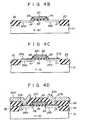
- a field oxide film 22was formed on a p-type Si substrate 21.
- a gate oxide film 23 and a gate electrode 24consisting of poly-Si or metal silicide were formed on the substrate 21, followed by introducing As into the substrate 21 by ion implantation so as to form n +- type diffusion layers 25a and 25b forming source and drain regions, respectively, having a junction depth of 0.15 ⁇ m.
- a Si0 2 film 26was deposited on the entire surface, followed by applying an anisotropic etching to the Si0 2 film 26 so as to selectively leave the SiO 2 film 26 on the side walls of the gate electrode as shown in Fig. 4B.
- W films 27a, 27b and 27cwere selectively grown on the surfaces of the n + -type diffusion layers 25a, 25b and the gate electrode 24 by a low pressure vapor growth method using a mixture of WF 6 and H z as the feed gas (Fig. 4C). Vapor growth was carried out under a substrate temperature of 350°C, a H 2 /WF 6 molar ratio of 100, and a reaction chamber inner pressure of 0.2 mmHg (Torr). After vapor growth, a Si0 2 film 28 was deposited on the entire surface by a plasma CVD method using a mixture of N 2 0 and SiH4 as the feed gas. Then, contact holes were made in the Si0 2 film 28, followed by forming AI layers 29a, 29b as shown in Fig. 4D.
- the resultant MOSFETwas found to be free of deterioration in the junction characteristic regardless of the very shallow pn junction formed therein. Also the MOSFET exhibited an excellent operation performance because W layers were formed on the surfaces of the shallow diffusion layers and the gate electrode to reduce the resistance thereof.
Landscapes
- Engineering & Computer Science (AREA)
- General Physics & Mathematics (AREA)
- Physics & Mathematics (AREA)
- Condensed Matter Physics & Semiconductors (AREA)
- Manufacturing & Machinery (AREA)
- Computer Hardware Design (AREA)
- Microelectronics & Electronic Packaging (AREA)
- Power Engineering (AREA)
- General Chemical & Material Sciences (AREA)
- Chemical Kinetics & Catalysis (AREA)
- Chemical & Material Sciences (AREA)
- Electrodes Of Semiconductors (AREA)
- Internal Circuitry In Semiconductor Integrated Circuit Devices (AREA)
Description
- The present invention relates to a method of producing a semiconductor device, particularly, to a method of selectively forming a metal film on the surface of a semiconductor layer by a selective vapor growth technique.
- Polycrystalline silicon (polysilicon) is widely used as the material of the gate electrode and interconnection electrode of a MOS type integrated circuit. However, polysilicon, even if doped with an impurity such as phosphorus, has a resistivity 100 times or more as high as that of a metal such as Al, with the result that a further improvement in the operation speed of an integrated circuit is obstructed by the use of polysilicon. Also, the recent miniaturization of the element is accompanied by a decrease in the junction depth, leading to a high resistance of the diffusion layer such as the source or drain region. The high operation speed of the integrated circuit is also obstructed by the high resistance of the diffusion layer mentioned above.
- Recently, it is attempted to selectively form a metal film having a low resistivity on an electrode formed of polysilicon or on a semiconductor layer doped with an impurity, e.g, on a diffusion layer, by means of a vapor growth method. For example, a tungsten (W) film is selectively formed on a silicon or polysilicon layer by a vapor growth method using tungsten hexafluoride as the feed gas. For instance, selective low pressure CVD of tungsten is disclosed in the journal of Electrochemistry Society Volume 131 No. 6, pages 1427 to 1433.
- However, where a W layer is selectively grown on a diffusion layer formed in the surface region of a silicon substrate using, for example, an oxide film as a mask, a remarkable leak current takes place in the pn junction between the diffusion layer and the substrate, leading in some cases to a short circuiting. The deterioration of the junction property is rendered more serious as the junction depth is decreased. Thus, it is difficult to apply the above-noted method to a diffusion layer having a junction depth of 0.2 11m or less.
- An object of the present invention is to provide a method of producing a semiconductor device, comprising a vapor growth deposition step which permits a selective growth of a metal film even on a semiconductor layer having a shallow pn junction without deteriorating the junction characteristics.
- As a result of extensive research on the above-noted conventional vapor growth deposition method of a metal film, the inventors have found that, in the vapor growth of a metal film on a diffusion layer formed in a semiconductor substrate with an insulating film used as a mask, the metal film extends from the edge of the insulating film to reach the interface between the insulating film and the diffusion layer, leading to a deterioration of the junction characteristics. The present invention has been achieved on the basis of this finding.
- According to the present invention, there is provided a method of manufacturing a semiconductor device, comprising the steps of: introducing an impurity of one conductivity type into a semiconductor substrate of an opposite conductivity type having an insulating film pattern formed a surface thereof, using the insulating film pattern used as a mask, to form a diffusion layer; and forming a metal film on the diffusion layer by selective vapor growth with a mixture of a metal source gas and a carrier gas used as a feed gas, said carrier gas being selected from the group consisting a hydrogen gas and an inert gas and the molar ratio of the carrier gas to the metal source gas is at least 50, said vapor growth being controlled by the substrate temperature and the metal source gas concentration, whereby the distance of entry of the metal film from the edge of the insulating film pattern to the interface between the insulating film pattern and the diffusion layer is smaller than the depth of the pn junction of the diffusion layer.
- Also, the flow rate of the metal source gas should desirably be 10 cc/min or less. A metal fluoride gas such as WF6 or MoF6 is used as the metal source gas. On the other hand, a H2 gas as well as an inert gas such as Ar or He, or a mixture of H2 gas and an inert gas is used as the additive gas.
- In the present invention, the insulating film pattern is used not only as a mask for introducing an impurity but also as a mask for the selective vapor growth of a metal. The insulating film pattern may be formed by patterning a silicon dioxide film formed on the semiconductor substrate. Alternatively, selective oxidation may be applied to a silicon substrate using a silicon nitride film pattern formed on the substrate as a mask. Further, the grooves formed on the substrate surface may be filled with an insulating material by a vapor growth so as to form the desired insulating film pattern.
- The diffusion layer may be formed by introducing As into a p-type silicon substrate. Alternatively, B (boron) may be introduced into an n-type silicon substrate to form the diffusion layer in the substrate.
- The substrate used in the present invention is not restricted to a silicon substrate. For example, a compound semiconductor substrate such as GaAs may also be used in the present invention.
- The method of the present invention makes it possible to selectively form a metal film on the surface of a diffusion layer without deteriorating the pn junction characteristics, leading to the production of a semiconductor device of a high reliability having a shallow pn junction and a diffusion layer of a low resistance.
- This invention can be more fully understood from the following detailed description when taken in conjunction with the accompanying drawings, in which:
- Fig. 1 is a cross-sectional view showing a semiconductor substrate provided with a diffusion layer having a metal film formed on the surface, said substrate used in the Experiment described herein;
- Fig. 2 is a graph showing the relationship between the vapor growth time and the distance of W entry;
- Fig. 3 shows the pn junction characteristics relative to the substrate temperature and the H2/ WF6 molar ratio; and
- Figs. 4A to 4D are cross-sectional views collectively showing a method of producing a MOS type semiconductor device according to one embodiment of the present invention.
- The following Experiment was conducted in order to determine the vapor growth condition employed in the method of the present invention.
- As shown in Fig. 1, a desired pattern of Si02 film 12 was formed on the surface of a p-type silicon substrate 11, followed by diffusing As (arsenic) into the exposed substrate 11 to form an n+-
type diffusion layer 13 having a pn junction depth of 0.1 to 0.3 pm. Then, aW film 14 having a thickness of 300 to 1,300×10-10m (A) was selectively grown on the surface of the n+-type diffusion layer 13 by a vapor growth method using a mixture of a WF6 gas and a H2 gas as the feed gas. A low pressure vapor growth apparatus of a diffusion furnace type was used for the vapor growth. The pressure within the reaction chamber for the vapor growth was set at 0.1 mmHg (Torr). Also, the total flow rate of WF6 and H2 was set at 200 cc/min. Fig. 2 shows the distance of entry with time of theW film 14 from the edge of the SiO2film 12 facing the opening made in thefilm 12 to the interface between the Si substrate and the SiO2 film, covering the cases where the substrate temperature was set at 150 to 800°C and the H2/ WF6 molar ratio at 10 to 1,000. - As apparent from Fig. 2, the W entry takes place in the initial stage of the W film growth and reaches saturation only several minutes after initiation. In the initial stage of the vapor growth during which the grown W film is very thin, a large amount of Si is thought to be consumed by the substitution reaction between WF6 and Si, with the result that a clearance is formed in the interface between the Si substrate and the SiO2 layer. Naturally, W is thought to enter the clearance. Several minutes after initiation of the vapor growth, however, the W film is thought to grow thick enough to fill the clearance mentioned above. In other words, the W entry in question is thought to reach saturation. Fig. 2 shows that the distance of the W entry is promoted as the substrate temperature is increased. Also, the W entry is increased in proportion to the decrease in the H2/WF6 molar ratio, i.e., the increase in the WF6 concentration.
- Where the junction depth of the n+-
type diffusion layer 13 shown in Fig. 1 is 0.2 µm, the lateral distance between the edge of the Si02 film 12 facing the opening made in thefilm 12 and the junction is also 0.2 µm. Thus, the distance of the W entry should be made 0.2 µm or less in order to prevent the short-circuiting of the junction. It follows that the substrate temperature should be set at 400°C or less and that the H2/WF6 molar ratio should be set at 50 or more in order to prevent the short-circuiting of the pn junction, as apparent from Fig. 2. - Fig. 3 shows the pn junction characteristics relative to the substrate temperature and the Hz/ WF6 molar ratio covering the case where the
W film 14 is formed by vapor growth on the n+-type diffusion layer 13 having the minimum junction depth of 0.1 to 0.2 µm. It should be noted that a W film is not grown if the substrate temperature is lower than 200°C. As apparent from Fig. 3, the substrate temperature should be 200 to 400°C and the H2/WF6 molar ratio should be at least 50 in order to grow a W film and to obtain the normal pn junction characteristics. Naturally, the normal pn junction characteristics can be obtained under the substrate temperature and the H2/WF6 molar ratio specified above even if the junction depth is more than 0.2 um. - The present invention can be more fully understood from the Example described in the following with reference to Figs. 4A to 4D.
- As seen from Fig. 4A, a
field oxide film 22 was formed on a p-type Si substrate 21. Then, agate oxide film 23 and agate electrode 24 consisting of poly-Si or metal silicide were formed on thesubstrate 21, followed by introducing As into thesubstrate 21 by ion implantation so as to form n+-type diffusion layers diffusion layers W films 27a, 27b and 27c were selectively grown on the surfaces of the n+-type diffusion layers gate electrode 24 by a low pressure vapor growth method using a mixture of WF6 and Hz as the feed gas (Fig. 4C). Vapor growth was carried out under a substrate temperature of 350°C, a H2/WF6 molar ratio of 100, and a reaction chamber inner pressure of 0.2 mmHg (Torr). After vapor growth, a Si02 film 28 was deposited on the entire surface by a plasma CVD method using a mixture of N20 and SiH4 as the feed gas. Then, contact holes were made in the Si02 film 28, followed by formingAI layers - The resultant MOSFET was found to be free of deterioration in the junction characteristic regardless of the very shallow pn junction formed therein. Also the MOSFET exhibited an excellent operation performance because W layers were formed on the surfaces of the shallow diffusion layers and the gate electrode to reduce the resistance thereof.
Claims (6)
1. A method of manufacturing a semiconductor device, comprising of the seps of:
introducing an impurity of one conductivity type into a semiconductor substrate of an opposite conductivity type having an insulating film pattern formed on the surface thereof, using the insulating film pattern as a mask to form a diffusion layer; forming a metal film on the diffusion layer by selective vapor growth with a mixture of a metal source gas a carrier gas used as a feed gas, said carrier gas being selected from the group consisting a hydrogen gas and an inert gas, and the molar ratio of the carrier gas to the metal source gas is at least 50, said vapor growth being controlled by the substrate temperature and the metal source gas concentration, whereby the distance of entry of the metal film from the edge of the insulating film pattern to the interface between the insulating film pattern and the diffusion layer is smaller than the depth of the pn junction of the diffusion layer.
2. A method according to claim 1, characterized in that the substrate temperature lies in the range 200 to 400°C.
3. A method according to claim 1 or claim 2 characterized in that the metal source gas is a metal fluoride gas.
4. A method according to claim 1, characterized in that the flow rate of the metal source gas is 10 cc/min or less.
5. The method according to claim 1, characterized in that the insulating film pattern consists of Si02.
6. The method according to claim 1, characterized in that the vapor growth is carried out under a reduced pressure.
Applications Claiming Priority (2)
| Application Number | Priority Date | Filing Date | Title |
|---|---|---|---|
| JP58158713AJPS6050920A (en) | 1983-08-30 | 1983-08-30 | Manufacture of semiconductor device |
| JP158713/83 | 1983-08-30 |
Publications (3)
| Publication Number | Publication Date |
|---|---|
| EP0147913A2 EP0147913A2 (en) | 1985-07-10 |
| EP0147913A3 EP0147913A3 (en) | 1987-10-14 |
| EP0147913B1true EP0147913B1 (en) | 1990-10-24 |
Family
ID=15677724
Family Applications (1)
| Application Number | Title | Priority Date | Filing Date |
|---|---|---|---|
| EP84305652AExpiredEP0147913B1 (en) | 1983-08-30 | 1984-08-20 | Method of producing a semiconductor device comprising a selective vapour growth technique |
Country Status (4)
| Country | Link |
|---|---|
| US (1) | US4597167A (en) |
| EP (1) | EP0147913B1 (en) |
| JP (1) | JPS6050920A (en) |
| DE (1) | DE3483466D1 (en) |
Families Citing this family (19)
| Publication number | Priority date | Publication date | Assignee | Title |
|---|---|---|---|---|
| JPS61274345A (en)* | 1985-05-29 | 1986-12-04 | Toshiba Corp | Manufacturing method of semiconductor device |
| JPS6231116A (en)* | 1985-08-02 | 1987-02-10 | Toshiba Corp | Manufacturing method of semiconductor device |
| GB2183090B (en)* | 1985-10-07 | 1989-09-13 | Canon Kk | Method for selective formation of deposited film |
| US4741928A (en)* | 1985-12-27 | 1988-05-03 | General Electric Company | Method for selective deposition of tungsten by chemical vapor deposition onto metal and semiconductor surfaces |
| US5324536A (en)* | 1986-04-28 | 1994-06-28 | Canon Kabushiki Kaisha | Method of forming a multilayered structure |
| US4849377A (en)* | 1986-05-27 | 1989-07-18 | General Electric Company | Active area planarization with self-aligned contacts |
| EP0268654A1 (en)* | 1986-06-16 | 1988-06-01 | AT&T Corp. | Method for fabricating devices using chemical vapour deposition, and devices formed thereby |
| US4968644A (en)* | 1986-06-16 | 1990-11-06 | At&T Bell Laboratories | Method for fabricating devices and devices formed thereby |
| FR2624304B1 (en)* | 1987-12-04 | 1990-05-04 | Philips Nv | METHOD FOR ESTABLISHING AN ELECTRICAL INTERCONNECTION STRUCTURE ON A SILICON SEMICONDUCTOR DEVICE |
| US5212400A (en)* | 1988-02-18 | 1993-05-18 | International Business Machines Corporation | Method of depositing tungsten on silicon in a non-self-limiting CVD process and semiconductor device manufactured thereby |
| US5071788A (en)* | 1988-02-18 | 1991-12-10 | International Business Machines Corporation | Method for depositing tungsten on silicon in a non-self-limiting CVD process and semiconductor device manufactured thereby |
| CA1308496C (en)* | 1988-02-18 | 1992-10-06 | Rajiv V. Joshi | Deposition of tungsten on silicon in a non-self-limiting cvd process |
| GB2215126B (en)* | 1988-02-19 | 1990-11-14 | Gen Electric Co Plc | Process for manufacturing a thin film transistor |
| US5149672A (en)* | 1988-08-01 | 1992-09-22 | Nadia Lifshitz | Process for fabricating integrated circuits having shallow junctions |
| US5006476A (en)* | 1988-09-07 | 1991-04-09 | North American Philips Corp., Signetics Division | Transistor manufacturing process using three-step base doping |
| US5021363A (en)* | 1989-09-07 | 1991-06-04 | Laboratories Incorporated | Method of selectively producing conductive members on a semiconductor surface |
| US5388577A (en)* | 1990-06-08 | 1995-02-14 | Boston University | Electrode array microchip |
| GB2253090A (en)* | 1991-02-22 | 1992-08-26 | Westinghouse Brake & Signal | Electrical contacts for semiconductor devices |
| US5888890A (en)* | 1994-08-12 | 1999-03-30 | Lg Semicon Co., Ltd. | Method of manufacturing field effect transistor |
Family Cites Families (11)
| Publication number | Priority date | Publication date | Assignee | Title |
|---|---|---|---|---|
| DE1900119B2 (en)* | 1969-01-02 | 1977-06-30 | Siemens AG, 1000 Berlin und 8000 München | PROCESS FOR DEPOSITING HIGH-MELTING CONTACT METAL LAYERS AT LOW TEMPERATURES |
| US3801365A (en)* | 1971-08-05 | 1974-04-02 | Energy Conversion Devices Inc | Method for producing an electrical device |
| JPS5099267A (en)* | 1973-12-28 | 1975-08-06 | ||
| JPS53114350A (en)* | 1977-03-16 | 1978-10-05 | Toshiba Corp | Semiconductor and its manufacture |
| US4313971A (en)* | 1979-05-29 | 1982-02-02 | Rca Corporation | Method of fabricating a Schottky barrier contact |
| JPS5776833A (en)* | 1980-09-04 | 1982-05-14 | Applied Materials Inc | Heat resistant metal depositing method and product thereof |
| US4404235A (en)* | 1981-02-23 | 1983-09-13 | Rca Corporation | Method for improving adhesion of metal film on a dielectric surface |
| US4343676A (en)* | 1981-03-26 | 1982-08-10 | Rca Corporation | Etching a semiconductor material and automatically stopping same |
| US4349408A (en)* | 1981-03-26 | 1982-09-14 | Rca Corporation | Method of depositing a refractory metal on a semiconductor substrate |
| US4517225A (en)* | 1983-05-02 | 1985-05-14 | Signetics Corporation | Method for manufacturing an electrical interconnection by selective tungsten deposition |
| US4532702A (en)* | 1983-11-04 | 1985-08-06 | Westinghouse Electric Corp. | Method of forming conductive interconnection between vertically spaced levels in VLSI devices |
- 1983
- 1983-08-30JPJP58158713Apatent/JPS6050920A/enactivePending
- 1984
- 1984-08-16USUS06/641,191patent/US4597167A/ennot_activeExpired - Lifetime
- 1984-08-20EPEP84305652Apatent/EP0147913B1/ennot_activeExpired
- 1984-08-20DEDE8484305652Tpatent/DE3483466D1/ennot_activeExpired - Lifetime
Also Published As
| Publication number | Publication date |
|---|---|
| US4597167A (en) | 1986-07-01 |
| EP0147913A3 (en) | 1987-10-14 |
| JPS6050920A (en) | 1985-03-22 |
| DE3483466D1 (en) | 1990-11-29 |
| EP0147913A2 (en) | 1985-07-10 |
Similar Documents
| Publication | Publication Date | Title |
|---|---|---|
| EP0147913B1 (en) | Method of producing a semiconductor device comprising a selective vapour growth technique | |
| US4873205A (en) | Method for providing silicide bridge contact between silicon regions separated by a thin dielectric | |
| US5378652A (en) | Method of making a through hole in multi-layer insulating films | |
| US5751050A (en) | Semiconductor device having a polysilicon resistor element with increased stability and method of fabricating same | |
| US4375999A (en) | Method of manufacturing a semiconductor device | |
| US5332691A (en) | Method of forming a contact | |
| US6093589A (en) | Methods for preventing gate oxide degradation | |
| EP0091984B1 (en) | Integrated circuit devices comprising dielectric isolation regions and methods for making such devices | |
| US5244835A (en) | Method of making contact electrodes of polysilicon in semiconductor device | |
| EP0328970B1 (en) | Method of depositing tungsten on silicon in a non-self-limiting CVD process and semi-conductor device manufactured thereby | |
| US5071788A (en) | Method for depositing tungsten on silicon in a non-self-limiting CVD process and semiconductor device manufactured thereby | |
| US4900689A (en) | Method of fabrication of isolated islands for complementary bipolar devices | |
| KR900001654B1 (en) | Semiconductor device manufacturing method | |
| US5291058A (en) | Semiconductor device silicon via fill formed in multiple dielectric layers | |
| CN1606800A (en) | Composite spacer liner for improved transistor performance | |
| CA1208805A (en) | Vertically isolated complementary transistors | |
| US6441444B1 (en) | Semiconductor device having a nitride barrier for preventing formation of structural defects | |
| US4968644A (en) | Method for fabricating devices and devices formed thereby | |
| US5212400A (en) | Method of depositing tungsten on silicon in a non-self-limiting CVD process and semiconductor device manufactured thereby | |
| US6200871B1 (en) | High performance self-aligned silicide process for sub-half-micron semiconductor technologies | |
| US6232192B1 (en) | Method of manufacturing semiconductor device having sidewall portions removed | |
| US5759905A (en) | Semiconductor processing method of forming a conductively doped semiconductive material plug within a contact opening | |
| US5913115A (en) | Method for producing a CMOS circuit | |
| EP0104079B1 (en) | Integrated circuit contact structure | |
| JP2685033B2 (en) | MIS type FET and manufacturing method thereof |
Legal Events
| Date | Code | Title | Description |
|---|---|---|---|
| PUAI | Public reference made under article 153(3) epc to a published international application that has entered the european phase | Free format text:ORIGINAL CODE: 0009012 | |
| 17P | Request for examination filed | Effective date:19840831 | |
| AK | Designated contracting states | Designated state(s):DE FR GB | |
| PUAL | Search report despatched | Free format text:ORIGINAL CODE: 0009013 | |
| AK | Designated contracting states | Kind code of ref document:A3 Designated state(s):DE FR GB | |
| 17Q | First examination report despatched | Effective date:19890424 | |
| GRAA | (expected) grant | Free format text:ORIGINAL CODE: 0009210 | |
| AK | Designated contracting states | Kind code of ref document:B1 Designated state(s):DE FR GB | |
| PG25 | Lapsed in a contracting state [announced via postgrant information from national office to epo] | Ref country code:FR Effective date:19901024 | |
| REF | Corresponds to: | Ref document number:3483466 Country of ref document:DE Date of ref document:19901129 | |
| EN | Fr: translation not filed | ||
| PG25 | Lapsed in a contracting state [announced via postgrant information from national office to epo] | Ref country code:GB Effective date:19910820 | |
| PLBE | No opposition filed within time limit | Free format text:ORIGINAL CODE: 0009261 | |
| STAA | Information on the status of an ep patent application or granted ep patent | Free format text:STATUS: NO OPPOSITION FILED WITHIN TIME LIMIT | |
| 26N | No opposition filed | ||
| GBPC | Gb: european patent ceased through non-payment of renewal fee | ||
| PGFP | Annual fee paid to national office [announced via postgrant information from national office to epo] | Ref country code:DE Payment date:20030828 Year of fee payment:20 |