EP0146709B1 - Pressure sensor - Google Patents
Pressure sensorDownload PDFInfo
- Publication number
- EP0146709B1 EP0146709B1EP84112321AEP84112321AEP0146709B1EP 0146709 B1EP0146709 B1EP 0146709B1EP 84112321 AEP84112321 AEP 84112321AEP 84112321 AEP84112321 AEP 84112321AEP 0146709 B1EP0146709 B1EP 0146709B1
- Authority
- EP
- European Patent Office
- Prior art keywords
- semiconductor
- pressure sensor
- pressure sensing
- pressure
- major surface
- Prior art date
- Legal status (The legal status is an assumption and is not a legal conclusion. Google has not performed a legal analysis and makes no representation as to the accuracy of the status listed.)
- Expired - Lifetime
Links
Images


Classifications
- G—PHYSICS
- G01—MEASURING; TESTING
- G01L—MEASURING FORCE, STRESS, TORQUE, WORK, MECHANICAL POWER, MECHANICAL EFFICIENCY, OR FLUID PRESSURE
- G01L9/00—Measuring steady of quasi-steady pressure of fluid or fluent solid material by electric or magnetic pressure-sensitive elements; Transmitting or indicating the displacement of mechanical pressure-sensitive elements, used to measure the steady or quasi-steady pressure of a fluid or fluent solid material, by electric or magnetic means
- G01L9/0041—Transmitting or indicating the displacement of flexible diaphragms
- G01L9/0051—Transmitting or indicating the displacement of flexible diaphragms using variations in ohmic resistance
- G01L9/0052—Transmitting or indicating the displacement of flexible diaphragms using variations in ohmic resistance of piezoresistive elements
- G01L9/0054—Transmitting or indicating the displacement of flexible diaphragms using variations in ohmic resistance of piezoresistive elements integral with a semiconducting diaphragm
- G—PHYSICS
- G01—MEASURING; TESTING
- G01L—MEASURING FORCE, STRESS, TORQUE, WORK, MECHANICAL POWER, MECHANICAL EFFICIENCY, OR FLUID PRESSURE
- G01L9/00—Measuring steady of quasi-steady pressure of fluid or fluent solid material by electric or magnetic pressure-sensitive elements; Transmitting or indicating the displacement of mechanical pressure-sensitive elements, used to measure the steady or quasi-steady pressure of a fluid or fluent solid material, by electric or magnetic means
- G01L9/0041—Transmitting or indicating the displacement of flexible diaphragms
- G01L9/0042—Constructional details associated with semiconductive diaphragm sensors, e.g. etching, or constructional details of non-semiconductive diaphragms
- H—ELECTRICITY
- H10—SEMICONDUCTOR DEVICES; ELECTRIC SOLID-STATE DEVICES NOT OTHERWISE PROVIDED FOR
- H10N—ELECTRIC SOLID-STATE DEVICES NOT OTHERWISE PROVIDED FOR
- H10N30/00—Piezoelectric or electrostrictive devices
- H10N30/20—Piezoelectric or electrostrictive devices with electrical input and mechanical output, e.g. functioning as actuators or vibrators
- H10N30/204—Piezoelectric or electrostrictive devices with electrical input and mechanical output, e.g. functioning as actuators or vibrators using bending displacement, e.g. unimorph, bimorph or multimorph cantilever or membrane benders
- H10N30/2041—Beam type
- H—ELECTRICITY
- H10—SEMICONDUCTOR DEVICES; ELECTRIC SOLID-STATE DEVICES NOT OTHERWISE PROVIDED FOR
- H10N—ELECTRIC SOLID-STATE DEVICES NOT OTHERWISE PROVIDED FOR
- H10N30/00—Piezoelectric or electrostrictive devices
- H10N30/80—Constructional details
- H10N30/87—Electrodes or interconnections, e.g. leads or terminals
- H—ELECTRICITY
- H10—SEMICONDUCTOR DEVICES; ELECTRIC SOLID-STATE DEVICES NOT OTHERWISE PROVIDED FOR
- H10N—ELECTRIC SOLID-STATE DEVICES NOT OTHERWISE PROVIDED FOR
- H10N39/00—Integrated devices, or assemblies of multiple devices, comprising at least one piezoelectric, electrostrictive or magnetostrictive element covered by groups H10N30/00 – H10N35/00
Definitions
- the present inventionrelates to a semiconductor device with pressure sensing elements, and more particularly to a silicon diaphragm type pressure sensor.
- the semiconductor pressure sensorallows to expect microminiaturization, reduced cost and enhanced performance.
- the silicon diaphragm type pressure sensoris typical of the semiconductor pressure sensor.
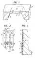
- a depressed portion 2is formed by etching the rear surface (side 1B) of a silicon single-crystal substrate 1, so as to use a membrane or thin-walled portion 3 as a diaphragm, and elongate diffused resistor layers 4 connected into a bridge are disposed in the major surface of the diaphragm 3.
- a pressure differencedevelops in spaces over and under the diaphragm, this diaphragm is deformed in accordance with the pressure difference.
- the diffused resistor layersexpand or shrink to change their resistances.
- the pressure sensorsenses a pressure change by electrically detecting the change of the resistances.
- Figure 2is a view showing the structure of a pressure sensing element which has been thought out by the inventors prior to the present invention.
- metal electrodes 7made of aluminum or the like are connected through contact holes 6 to the diffused resistor layer 4 serving as the pressure sensing element.
- the diffused resistor layer 4whose corner part is bent in the shape of the letter U is formed in the major surface ((100) plane) of the diaphragm 3, and it is held in ohmic contact with the aluminum leads 7 through the contact holes 6.
- the aluminum leads 7are extended as wiring leads on the front surface of the thick-walled semiconductor body 1 around the diaphragm 3.
- Figure 4is a plan view schematically showing the silicon diaphragm portion
- Figures 5(a) and 6(a)are sectional views taken along lines A-A' and B ⁇ B' in Figure 4, respectively.
- the resistor 4a of the corner partundergoes a stress as indicated by arrows in Figure 5(a).
- the resistors 4b of the straight parts which perform an actual pressure sensing operationundergo stresses as indicated by arrows in Figure 6(a).
- Figures 5(b) and 5(c) and Figures 6(b) and 6(c)are views which show in plan the changes of the shapes of the respective resistors 4a and 4b before and after the deformation of the diaphragm.
- the resistor 4ahas the relations of W I >W 2 and R, ⁇ R 2 where W 1 denotes the width of this resistor before the deformation of the diaphragm and R 1 the resistance thereof at that time, and W 2 denotes the width of this resistor after the deformation of the diaphragm and R 2 the resistance thereof at that time.
- each resistor 4bhas the relations of W 3 ⁇ W 4 and R 3 >R 4 where W 3 denotes the width of this resistor before the deformation of the diaphragm and R 3 the resistance thereof at that time, and W 4 denotes the width of this resistor after the deformation of the diaphragm and R 4 the resistance thereof at that time.
- Figure 3is a sectional view taken along line A-A' in Figure 2.
- Figure 3wherein aluminum is directly connected to the resistor layer 4 on the silicon diaphragm, there is the problem that a precise pressure measurement is impossible on account of a strain which arises between the aluminum 7 and an oxide film (Si0 2 film) 8 on the silicon surface.
- Si0 2 filmoxide film
- the strain of the grain boundary of the aluminumstresses the Si0 2 film and the surface of the silicon membrane portion directly below it, with the result that residual strains develop in the diaphragm surface (as indicated by T in Figure 3). It has been revealed that the residual strains exert the evil effects of causing variation in the characteristics of the diaphragm type pressure sensors, etc. and that they set limits to the provision of a pressure sensor of high precision.
- the p--type resistor layer 4is unitarily formed, and hence, the resistance Ra of the corner part thereof is comparatively high.
- Rbdenote the resistance of the straight part of the resistor layer 4
- ⁇ Rbdenote the variation of the resistance Rb based on the deformation of the silicon diaphragm
- the pressure sesnsitivity a of the pressure sensoris substantially given by the following equation: As understood from Equation (1), when the resistance Ra is high, the pressure sensitivity a becomes low.
- the present inventionhas been made in view of the aforementioned problems, and has for its object to provide a semiconductor pressure sensor which exhibits a high sensitivity and a high performance.
- the present inventionis constructed as follows:
- the object of the present inventioncan be accomplished.
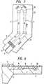
- Figure 7illustrates one embodiment of the present invention and is a plan view showing diffused resistor layers 4 as well as lead-out portions 9 in the pressure sensing element of a silicon diaphragm pressure sensor, while Figure 8 is a sectional view of the diffused resistor layer 4 as well as the lead-out portion 9 on one side shown in Figure 7, taken along the longitudinal direction thereof.
- Each p-type diffused resistor layer 4is formed in the major surface (100) of a diaphragm 3 which is made of an n-type semiconductor (silicon single crystal).
- Each electrode lead-out portion 9is made of a heavily-doped p +- type diffused layer, and is connected with one end of the corresponding p-type diffused resistor layer by overlapping it.
- An aluminum lead 7lies in ohmic contact with the electrode lead-out portion 9 in the place where the latter is led outside the diaphragm 3 (to the peripheral part of a semiconductor body 1).
- the electrode lead-out portions 9 made of the heavily-doped p +- type diffused layers, and a p + diffused layer 10 forming the corner part of the pressure sensing elementare arrayed in the direction of the crystal axis ⁇ 100> or ⁇ 010>.
- Figure 9is a diagram of the orientation- dependence curves of piezoresistive coefficients in the surface of a semiconductor wafer equivalent to the (100) plane.
- the expression "surface equivalent to the (100) plane”signifies the (100), (010) and (001) planes and crystal planes parallel thereto. These planes have the same physical properties, and are generally indicated by the representative plane (100) in this specification.
- the major surface of the semiconductor body 1 (the diaphragm 3) in Figure 9is the (001) plane in the concrete.
- parts denoted by [ ]indicate for reference the corresponding crystal orientations in the case where the (100) plane is used as the major surface of the semiconductor body 1 in the concrete.
- the pressure sensing resistorundergoes two stresses in the longitudinal direction of the resistor and in the direction orthogonal thereto, and the piezoresistive coefficients concerning the respective stresses are denoted by ⁇ 1 and ⁇ t .
- Letting 6 1 and 5denote the stresses in the longitudinal direction of the resistor and the transerse direction orthogonal thereto, respectively, the pressure sensitivity is expressed by
- the crystal orientation dependence of the piezoresistive coefficient ⁇ 1is indicated by a solid line
- that of the piezoresistive coefficient ⁇ tis indicated by a dotted line.
- both the coefficients ⁇ 1 and ⁇ texhibit the maximum values in the directions ⁇ 110> and ⁇ 110>.
- theyassume the minimum values in the directions ⁇ 100> and ⁇ 010>.
- the p-type diffused resistor layers 4pressure sensing semiconductor strips which are the straight parts of the pressure sensing element of the embodiment illustrated in Figure 7 are extended in the direction ⁇ 110> or ⁇ 110> in which the maximum resistance variation is exhibited.
- the heavily-doped p +- type diffused layers 9 serving as the electrode lead-out portions and the p + -type diffused layer 10 for connecting the other ends of the pair of p-type diffused resistor layers 4are formed in the direction ⁇ 100> or ⁇ 010> which define angles of 45 degrees to the aforementioned direction and in which the minimum resistance variation is exhibited.
- the p-type diffused layer 4 constituting the pressure sensing elementhas the greatest piezoresistive coefficient, it has its resistance varied greatly by a strain which develops due to the deformation of the silicon diaphragm. That is, it is very sensitive to a pressure or the like.
- the heavily-doped p + diffused layers 9 and 10are arranged in the orientation of the minimum piezoresistive coefficient, they are the most insensitive to a pressure change. With the above construction, the pressure change is detected as the variation of the resistance of the p-type resistor layer 4 sensitively and at high precision, and the reduction of the resistance variation attributed to the heavily-doped p + diffused layers 9 and 10 is suppressed to be the least. It is therefore possible to provide a silicon diaphragm type pressure sensor of high precision and high reliability.
- the resistor layers other than the resistor layers 4 functioning as the pressure sensing elementthat is, the electrode lead-out resistor layers 9 and the resistor layer 10 of the corner part are formed of the p + diffused layers of low resistivity in which an impurity is introduced at a high concentration. Therefore, the pressure sensitivity a can be enhanced.
- the contact portion between the aluminum electrode 7 and the electrode lead-out resistor layer 9is not formed in the major surface of the silicon diaphragm 3, but it is formed in the peripheral part of the semiconductor body 1 off the diaphragm. Therefore, the influence which is exerted on the deformation of the silicon diaphragm by the residual stress developing in the vicinity of the contact portion can be minimized.
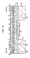
- Figure 10is a schematic top view of the diaphragm type pressure sensor.
- the pressure sensing elementsare disposed in four places, the diffused resistor layers 4 have their longitudinal direction arranged in the direction of the ⁇ 110> axis, and the heavily-doped diffused lead-out portions 9 and the heavily-doped diffused corner parts 10 are formed by setting their longitudinal directions at the direction of the ⁇ 100> or ⁇ 010> axis.
- the resistance variation of the diffused resistor layers resulting from the pressure difference between spaces over and under the diaphragm 3is electrically detected to measure a pressure.
- the arrangement orientations of the resistor layers of the corner part, electrode lead-out portions and pressure sensing portions (straight parts) in the pressure sensing elementare not restricted to the orientations mentioned before.
- Figure 11illustrates the variations of the piezoresistive coefficients "1 and ⁇ t in the case where the (110) plane (or a plane equivalent to the (110) plane) is employed as the major surface of a semiconductor wafer.
- the expression "plane equivalent to the (110) plane”signifies the (110), (110) and (110) planes and planes parallel thereto, and they are generally termed the (110) plane in this specification. Concretely or strictly speaking, the major surface of the semiconductor wafer depicted in Figure 11 is the (110) plane.
- the pressure sensing elementis arranged in orientations illustrated in Figure 12 by way of example. That is, pressure sensing portions 4' made of p--type diffused resistor layers are arranged in the ⁇ 111> direction in which the variations of the piezoresistive coefficients ⁇ t and ⁇ t are the greatest.
- a p +- type diffused layer 10' as the corner part and p +- type diffused layers 9' as the electrode lead-out portionsare arranged in the direction of the ⁇ 001> crystal axis in which the variations of the piezoresistive coefficients are the smallest.
- wiring leads 7' made of aluminum and the contact portions C 1 ' between them and the p +- type diffused layers 9'are provided on the thick-walled part of the semiconductor body outside the silicon diaphragm.
- Figures 13 and 14show a plan view of a pressure sensor in which pressure sensing elements and other active elements coexist on a single semiconductor body, and a sectional view taken along B-B' in Figure 13, respectively.
- a depressed portion 27 corresponding to a diaphragmis formed in the rear surface of a Si semiconductor body having the (100) plane (a Si epitaxial layer 21, a Si substrate 60), substantially at the central part thereof.
- a p +- type isolation layer 23 for isolating pressure sensing elements (active elements)is formed so as to surround the diaphragm.
- the respective sides of the diaphragm (27) surrounded with the isolation layer 23are formed with resistors (diffused resistors), R 1 , R 2 , R 3 and R 4 which are used as the pressure sensing elements.
- the resistorshave the same arrangements and are connected into a bridge by wiring layers 25. Next, the arrangement of each resistor will be explained by taking the resistor R 1 as an example.
- This resistor Ris composed of p-type diffused resistor layers 24 (sheet resistance: 100 ⁇ / ⁇ ) which are formed in the direction of the ⁇ 110> axis, p +- type diffused layers for contacts 28a (sheet resistance: 30 Q/D) which are formed in the direction of the ⁇ 100> axis inclining by 45 degrees with respect to the ⁇ 110> axis, and a p +- type diffused layer 28b (sheet resistance: 30 ⁇ / ⁇ ) which connects the p-type diffused resistor layers 24 extending in parallel with each other.
- the p +- type diffused layer 28ais in the direction of a small piezoresistive effect (in the direction of the ⁇ 100> axis or any axis equivalent thereto), and it is heavily doped, so that the fluctuation of its resistance versus the strain of the diaphragm is small and negligible. Further, the p +- type diffused layer 28b is heavily doped.
- p +- type diffused layers 28a and 28bare formed simultaneously with the emitter and collector regions 28 of a P-N-P transistor (PNP TRS.).
- PNP TRS.P-N-P transistor
- an n +- type diffused layer 30'is formed so as to enclose the p-type diffused resistor layers 24 and the p +- type diffused layers 28a, 28b.
- the n +- type diffused layers 30'are formed simultaneously with the emitter region 30a and collector contact region 30b of an N-P-N transistor (NPN TRS.) and the base contact region 30c of the P-N-P transistor.
- NPN TRS.N-P-N transistor
- the P-N-P transistor and the N-P-N transistor which are located near the periphery of the diaphragmconstitute a temperature compensation circuit, an amplifier circuit or the like.
- External lead-out terminals (bonding pads) 35are disposed in the periphery of the semiconductbr body.
- the present inventionis applicable to any of silicon diaphragm type pressure sensors employing p-type diffused resistor layers and diaphragm type pressure sensors including ICs.
- the pressure sensor according to the present inventionis very effective when applied to pressure control circuits in an automobile, a musical instrument, etc.
Landscapes
- Physics & Mathematics (AREA)
- General Physics & Mathematics (AREA)
- Chemical & Material Sciences (AREA)
- Analytical Chemistry (AREA)
- Pressure Sensors (AREA)
- Measuring Fluid Pressure (AREA)
Description
- The present invention relates to a semiconductor device with pressure sensing elements, and more particularly to a silicon diaphragm type pressure sensor.
- Unlike past mechanical pressure sensors employing a Bourdon tube etc., the semiconductor pressure sensor allows to expect microminiaturization, reduced cost and enhanced performance. The silicon diaphragm type pressure sensor is typical of the semiconductor pressure sensor.
- The structure of the silicon diaphragm type pressure sensor will be briefly explained. As shown in Figure 1 a depressed portion 2 is formed by etching the rear surface (side 1B) of a silicon single-
crystal substrate 1, so as to use a membrane or thin-walledportion 3 as a diaphragm, and elongate diffusedresistor layers 4 connected into a bridge are disposed in the major surface of thediaphragm 3. When a pressure difference develops in spaces over and under the diaphragm, this diaphragm is deformed in accordance with the pressure difference. Owing to the deformation of the diaphragm, the diffused resistor layers expand or shrink to change their resistances. The pressure sensor senses a pressure change by electrically detecting the change of the resistances. - Figure 2 is a view showing the structure of a pressure sensing element which has been thought out by the inventors prior to the present invention. As illustrated in the figure, in the silicon diaphragm type pressure sensor,
metal electrodes 7 made of aluminum or the like are connected throughcontact holes 6 to the diffusedresistor layer 4 serving as the pressure sensing element. - In the structure of Figure 2, the diffused
resistor layer 4 whose corner part is bent in the shape of the letter U is formed in the major surface ((100) plane) of thediaphragm 3, and it is held in ohmic contact with the aluminum leads 7 through thecontact holes 6. The aluminum leads 7 are extended as wiring leads on the front surface of the thick-walled semiconductor body 1 around thediaphragm 3. - The inventors have recognized that the following problems are involved in the pressure sensor of such structure:
- (1) With the U-shaped diffused resistor layer as shown in Figure 2, the changes of the resistance caused by the deformation of the diaphragm are in senses opposite to each other between a straight part and the corner part and are cancelled, so that the resistance change of the whole diffused resistor becomes small. This will be elucidated with reference to Figure 4, Figures 5(a)-5(c) and Figures 6(a)-6(c).
- Figure 4 is a plan view schematically showing the silicon diaphragm portion, and Figures 5(a) and 6(a) are sectional views taken along lines A-A' and B―B' in Figure 4, respectively. Assuming that the
diaphragm 3 has been deformed downwards, theresistor 4a of the corner part undergoes a stress as indicated by arrows in Figure 5(a). On the other hand, theresistors 4b of the straight parts which perform an actual pressure sensing operation undergo stresses as indicated by arrows in Figure 6(a). Figures 5(b) and 5(c) and Figures 6(b) and 6(c) are views which show in plan the changes of the shapes of therespective resistors resistor 4a has the relations of WI>W2 and R,<R2 where W1 denotes the width of this resistor before the deformation of the diaphragm and R1 the resistance thereof at that time, and W2 denotes the width of this resistor after the deformation of the diaphragm and R2 the resistance thereof at that time. Meanwhile, as seen from Figures 6(b) and 6(c), eachresistor 4b has the relations of W3<W4 and R3>R4 where W3 denotes the width of this resistor before the deformation of the diaphragm and R3 the resistance thereof at that time, and W4 denotes the width of this resistor after the deformation of the diaphragm and R4 the resistance thereof at that time. - Thus, even when the pressure change is sensed as the change of the resistance by the
resistors 4b of the straight parts, the resistance change is cancelled because the change of the resistance in theresistor 4a of the corner part is opposite in sense to that in theresistor 4b of the straight part. Therefore, the sensitivity of the pressure sensor becomes low. - (2) Figure 3 is a sectional view taken along line A-A' in Figure 2. With the structure shown in Figure 3 wherein aluminum is directly connected to the
resistor layer 4 on the silicon diaphragm, there is the problem that a precise pressure measurement is impossible on account of a strain which arises between thealuminum 7 and an oxide film (Si02 film) 8 on the silicon surface. More specifically, since the difference between the coefficients of thermal expansion of the aluminum and the Si02 film is great, the strain of the grain boundary of the aluminum stresses the Si02 film and the surface of the silicon membrane portion directly below it, with the result that residual strains develop in the diaphragm surface (as indicated by T in Figure 3). It has been revealed that the residual strains exert the evil effects of causing variation in the characteristics of the diaphragm type pressure sensors, etc. and that they set limits to the provision of a pressure sensor of high precision. - (3) As shown in Figure 2, the p--
type resistor layer 4 is unitarily formed, and hence, the resistance Ra of the corner part thereof is comparatively high. Letting Rb denote the resistance of the straight part of theresistor layer 4, and ΔRb denote the variation of the resistance Rb based on the deformation of the silicon diaphragm, the pressure sesnsitivity a of the pressure sensor is substantially given by the following equation:
- The three problems mentioned above have been found by the inventors.
- The present invention has been made in view of the aforementioned problems, and has for its object to provide a semiconductor pressure sensor which exhibits a high sensitivity and a high performance.
- The present invention is constructed as follows:
- (1) The resistor region of a corner part in a pressure sensing resistor is formed along a crystal orientation whose pressure sensitivity is very low. Thus, the variation of a resistance to arise in the corner part is rendered very small, and the variation of a resistance in each straight part (termed "pressure sensing strip") of the pressure sensing resistor is detected substantially as it is. For example, in a semiconductor diaphragm type sensor whose major surface is the (100) plane of a silicon single-crystal substrate, the resistor layer of the corner part is formed in the direction of a crystal axis equivalent to <100> or <010>.
- (2) The contact portions between the pressure sensing resistor layer and AI leads are provided in a surrounding area outside a silicon diaphragm region. Thus, the influence which strains developing near the contact portions exert on a pressure sensing operation is lessened.
- (3) The resistor of the corner part in the pressure sensing resistor layer is formed of a p+ diffused layer so as to lower the resistance of this part. Thus, the pressure sensitivity is enhanced.
- Owing to the above construction, the object of the present invention can be accomplished.
- Figure 1 is a perspective view showing the structure of a silicon diaphragm type pressure sensor;
- Figure 2 is a plan view showing the pattern of a diffused resistor in a diaphragm type pressure sensor which was studied by the inventors before the present invention;
- Figure 3 is a sectional view taken along A-A' in Figure 2;
- Figure 4 is a plan view showing the pattern of the resistor shown in Figure 2, schematically and for elucidating the operation of the resistor;
- Figures 5(a), 5(b) and 5(c) are views for explaining the situation of the change of the resistance of a resistor (4a) in the case where a diaphragm has been deformed downwards in the pressure sensor illustrated in Figure 4;
- Figures 6(a), 6(b) and 6(c) are views for explaining the situation of the change of the resistance of a resistor (4b) in the case where the diaphragm has been deformed downwards in the pressure sensor illustrated in Figure 4;
- Figure 7 illustrates one embodiment of the present invention, and is a plan view showing the pattern of diffused resistor layers as well as lead-out portions in a pressure sensor;
- Figure 8 is a sectional view of the diffused resistor layer as well as the lead-out portion in Figure 7 as taken along the longitudinal direction thereof;
- Figure 9 is a curve diagram showing the orientation dependences of piezoresistive coefficients in the case where the major surface of a wafer is the (100) plane;
- Figure 10 is a plan view of the upper surface of the pressure sensor;
- Figure 11 is a curve diagram showing the orientation dependences of piezoresistive coefficients in the case where the major surface of a wafer is the (110) plane;
- Figure 12 is a plan view showing the plane pattern of pressure sensing resistor layers in the case where the major surface of the wafer is the (110) plane;
- Figure 13 illustrates still another embodiment of the present invention, and is a plan view of a pressure sensor including active elements; and
- Figure 14 is a sectional view taken along B-B' in Figure 13.
- Figure 7 illustrates one embodiment of the present invention and is a plan view showing diffused
resistor layers 4 as well as lead-outportions 9 in the pressure sensing element of a silicon diaphragm pressure sensor, while Figure 8 is a sectional view of the diffusedresistor layer 4 as well as the lead-outportion 9 on one side shown in Figure 7, taken along the longitudinal direction thereof. - Each p-type diffused
resistor layer 4 is formed in the major surface (100) of adiaphragm 3 which is made of an n-type semiconductor (silicon single crystal). Each electrode lead-outportion 9 is made of a heavily-doped p+-type diffused layer, and is connected with one end of the corresponding p-type diffused resistor layer by overlapping it. Analuminum lead 7 lies in ohmic contact with the electrode lead-outportion 9 in the place where the latter is led outside the diaphragm 3 (to the peripheral part of a semiconductor body 1). The electrode lead-outportions 9 made of the heavily-doped p+-type diffused layers, and a p+ diffusedlayer 10 forming the corner part of the pressure sensing element are arrayed in the direction of the crystal axis <100> or <010>. - Figure 9 is a diagram of the orientation- dependence curves of piezoresistive coefficients in the surface of a semiconductor wafer equivalent to the (100) plane. The expression "surface equivalent to the (100) plane" signifies the (100), (010) and (001) planes and crystal planes parallel thereto. These planes have the same physical properties, and are generally indicated by the representative plane (100) in this specification. The major surface of the semiconductor body 1 (the diaphragm 3) in Figure 9 is the (001) plane in the concrete. In the figure, parts denoted by [ ] indicate for reference the corresponding crystal orientations in the case where the (100) plane is used as the major surface of the
semiconductor body 1 in the concrete. - The pressure sensing resistor undergoes two stresses in the longitudinal direction of the resistor and in the direction orthogonal thereto, and the piezoresistive coefficients concerning the respective stresses are denoted by π1 and πt. Letting 61 and 5, denote the stresses in the longitudinal direction of the resistor and the transerse direction orthogonal thereto, respectively, the pressure sensitivity is expressed by

- As shown in the figure, both the coefficients π1 and πt exhibit the maximum values in the directions <110> and <110>. On the other hand, they assume the minimum values in the directions <100> and <010>. Accordingly, the p-type diffused resistor layers 4 (pressure sensing semiconductor strips) which are the straight parts of the pressure sensing element of the embodiment illustrated in Figure 7 are extended in the direction <110> or <110> in which the maximum resistance variation is exhibited. On the other hand, the heavily-doped p+-type diffused
layers 9 serving as the electrode lead-out portions and the p+-type diffusedlayer 10 for connecting the other ends of the pair of p-type diffusedresistor layers 4 are formed in the direction <100> or <010> which define angles of 45 degrees to the aforementioned direction and in which the minimum resistance variation is exhibited. - Since the p-type diffused
layer 4 constituting the pressure sensing element has the greatest piezoresistive coefficient, it has its resistance varied greatly by a strain which develops due to the deformation of the silicon diaphragm. That is, it is very sensitive to a pressure or the like. In contrast, since the heavily-doped p+ diffusedlayers type resistor layer 4 sensitively and at high precision, and the reduction of the resistance variation attributed to the heavily-doped p+ diffusedlayers - In addition, the resistor layers other than the resistor layers 4 functioning as the pressure sensing element, that is, the electrode lead-out
resistor layers 9 and theresistor layer 10 of the corner part are formed of the p+ diffused layers of low resistivity in which an impurity is introduced at a high concentration. Therefore, the pressure sensitivity a can be enhanced. - Besides, as shown in Figure 8, the contact portion between the
aluminum electrode 7 and the electrode lead-outresistor layer 9 is not formed in the major surface of thesilicon diaphragm 3, but it is formed in the peripheral part of thesemiconductor body 1 off the diaphragm. Therefore, the influence which is exerted on the deformation of the silicon diaphragm by the residual stress developing in the vicinity of the contact portion can be minimized. - Figure 10 is a schematic top view of the diaphragm type pressure sensor. As illustrated in the figure, the pressure sensing elements are disposed in four places, the diffused
resistor layers 4 have their longitudinal direction arranged in the direction of the <110> axis, and the heavily-doped diffused lead-outportions 9 and the heavily-doped diffusedcorner parts 10 are formed by setting their longitudinal directions at the direction of the <100> or <010> axis. By a circuit in which the pressure sensing elements in the four places shown in the figure are connected into a bridge by wiring, the resistance variation of the diffused resistor layers resulting from the pressure difference between spaces over and under thediaphragm 3 is electrically detected to measure a pressure. - The arrangement orientations of the resistor layers of the corner part, electrode lead-out portions and pressure sensing portions (straight parts) in the pressure sensing element are not restricted to the orientations mentioned before.
- Figure 11 illustrates the variations of the piezoresistive coefficients"1 and πt in the case where the (110) plane (or a plane equivalent to the (110) plane) is employed as the major surface of a semiconductor wafer. The expression "plane equivalent to the (110) plane" signifies the (110), (110) and (110) planes and planes parallel thereto, and they are generally termed the (110) plane in this specification. Concretely or strictly speaking, the major surface of the semiconductor wafer depicted in Figure 11 is the (110) plane. As apparent from the figure, in the case of selecting the (110) plane as the major surface of the wafer, the variations of the coefficients"1 and r4 do not correspond but the coefficient πt varies much more than the coefficient π1, unlike the case of the (100) plane. It is also seen that both the variations of the coefficients"1 and πt are great in the direction of the <111> crystal axis and that both the coefficients π1 and πt are minimized in the direction of the <100> crystal axis.
- Therefore, when the (110) plane is used as the major surface of the wafer, the pressure sensing element is arranged in orientations illustrated in Figure 12 by way of example. That is, pressure sensing portions 4' made of p--type diffused resistor layers are arranged in the <111> direction in which the variations of the piezoresistive coefficients πt and πt are the greatest. On the other hand, a p+-type diffused layer 10' as the corner part and p+-type diffused layers 9' as the electrode lead-out portions are arranged in the direction of the <001> crystal axis in which the variations of the piezoresistive coefficients are the smallest. As in
Embodiment 1, wiring leads 7' made of aluminum and the contact portions C1' between them and the p+-type diffused layers 9' are provided on the thick-walled part of the semiconductor body outside the silicon diaphragm. - The two embodiments described above bring forth the following effects:
- (1) The principal parts of a pressure sensing element are arranged in the crystal orientation of great piezoresistive coefficients, and the resistor layer of a corner part and the resistor layers of electrode lead-out portions are arranged in the orientation of the minimum piezoresistive coefficients, whereby the pressure sensitivity can be sharply enhanced.
- (2) Since the contact portions between electrodes of AI or the like and the electrode lead-out resistor layers are provided outside a diaphragm (thin-walled part), strains developing in an Si02 film etc. are prevented from affecting the deformation of the diaphragm, and the pressure sensitivity can be enhanced.
- (3) The resistor layers of the corner part and the electrode lead-out portions are rendered the p+- type of low resistivity, so that a pressure can be detected sensitively.
- Figures 13 and 14 show a plan view of a pressure sensor in which pressure sensing elements and other active elements coexist on a single semiconductor body, and a sectional view taken along B-B' in Figure 13, respectively.
- Referring to Figures 13 and 14, a
depressed portion 27 corresponding to a diaphragm is formed in the rear surface of a Si semiconductor body having the (100) plane (aSi epitaxial layer 21, a Si substrate 60), substantially at the central part thereof. A p+-type isolation layer 23 for isolating pressure sensing elements (active elements) is formed so as to surround the diaphragm. The respective sides of the diaphragm (27) surrounded with theisolation layer 23 are formed with resistors (diffused resistors), R1, R2, R3 and R4 which are used as the pressure sensing elements. As apparent from Figure 13, the resistors have the same arrangements and are connected into a bridge by wiring layers 25. Next, the arrangement of each resistor will be explained by taking the resistor R1 as an example. - This resistor R, is composed of p-type diffused resistor layers 24 (sheet resistance: 100 Ω/□) which are formed in the direction of the <110> axis, p+-type diffused layers for
contacts 28a (sheet resistance: 30 Q/D) which are formed in the direction of the <100> axis inclining by 45 degrees with respect to the <110> axis, and a p+- type diffusedlayer 28b (sheet resistance: 30 Ω/□) which connects the p-type diffused resistor layers 24 extending in parallel with each other. A diffused resistor which extends in the direction of the <110> axis or any axis equivalent thereto exhibits a great piezoresistive effect, and causes a resistance change sensitively to the strain of the diaphragm. Especially in the case of the resistor layer exhibiting the p-conductivity type, this is remarkable. In contrast, the p+-type diffusedlayer 28a is in the direction of a small piezoresistive effect (in the direction of the <100> axis or any axis equivalent thereto), and it is heavily doped, so that the fluctuation of its resistance versus the strain of the diaphragm is small and negligible. Further, the p+-type diffusedlayer 28b is heavily doped. These p+-type diffusedlayers collector regions 28 of a P-N-P transistor (PNP TRS.). In order to prevent the channel leakage between the resistors within the diaphragm, an n+-type diffused layer 30' is formed so as to enclose the p-type diffused resistor layers 24 and the p+-type diffusedlayers emitter region 30a andcollector contact region 30b of an N-P-N transistor (NPN TRS.) and thebase contact region 30c of the P-N-P transistor. The P-N-P transistor and the N-P-N transistor which are located near the periphery of the diaphragm constitute a temperature compensation circuit, an amplifier circuit or the like. External lead-out terminals (bonding pads) 35 are disposed in the periphery of the semiconductbr body. - According to this embodiment, the following effects are attained in addition to the effects mentioned before:
- (1) A p+-type buried
layer 18b (Figure 14) formed around the sensor portion can finish up an isolation region of small width when coupled with a p+-type diffusedlayer 23 which extends from the front surface of an epitaxial n-type Si layer. Therefore, the occupying area of the isolation region can be reduced, and a semiconductor device having a high density of integration can be produced. - (2) n+-type buried layers can be utilized as parts of active elements (the collector of the N-P-N transistor, the base of the lateral P-N-P transistor) in peripheral portions.
- (3) A Si membrane portion or diaphragm can be sufficiently thickened by rendering the epitaxial n-type Si layer thick whereby even a sensor applicable to a high pressure (100 Torr or above) can be manufactured at high precision.
- (4) An IC in which active elements of high withstand voltage and a pressure sensor applicable to a high pressure are integrally combined can be realized by the use of a thick n-type Si layer.
- The present invention is applicable to any of silicon diaphragm type pressure sensors employing p-type diffused resistor layers and diaphragm type pressure sensors including ICs.
- The pressure sensor according to the present invention is very effective when applied to pressure control circuits in an automobile, a musical instrument, etc.


Claims (12)
Applications Claiming Priority (2)
| Application Number | Priority Date | Filing Date | Title |
|---|---|---|---|
| JP236152/83 | 1983-12-16 | ||
| JP58236152AJPS60128673A (en) | 1983-12-16 | 1983-12-16 | Semiconductor pressure-sensing device |
Publications (3)
| Publication Number | Publication Date |
|---|---|
| EP0146709A2 EP0146709A2 (en) | 1985-07-03 |
| EP0146709A3 EP0146709A3 (en) | 1988-09-07 |
| EP0146709B1true EP0146709B1 (en) | 1990-07-18 |
Family
ID=16996528
Family Applications (1)
| Application Number | Title | Priority Date | Filing Date |
|---|---|---|---|
| EP84112321AExpired - LifetimeEP0146709B1 (en) | 1983-12-16 | 1984-10-12 | Pressure sensor |
Country Status (7)
| Country | Link |
|---|---|
| US (1) | US4672411A (en) |
| EP (1) | EP0146709B1 (en) |
| JP (1) | JPS60128673A (en) |
| KR (1) | KR930003148B1 (en) |
| DE (1) | DE3482753D1 (en) |
| HK (1) | HK107391A (en) |
| SG (1) | SG97391G (en) |
Cited By (8)
| Publication number | Priority date | Publication date | Assignee | Title |
|---|---|---|---|---|
| FR2594546A1 (en)* | 1986-02-19 | 1987-08-21 | Flopetrol | Device for measuring the temperature of the diaphragm of a pressure sensor |
| GB2187887A (en)* | 1986-03-10 | 1987-09-16 | Marelli Autronica | Thick-film sensor |
| EP0195232A3 (en)* | 1985-03-20 | 1989-10-25 | Hitachi, Ltd. | Piezoresistive strain sensing device |
| EP0340904A3 (en)* | 1988-05-02 | 1991-02-27 | DELCO ELECTRONICS CORPORATION (a Delaware corp.) | Monolithic pressure sensitive integrated circuit and a process for manufacture thereof |
| US6211772B1 (en) | 1995-01-30 | 2001-04-03 | Hitachi, Ltd. | Semiconductor composite sensor |
| US6234027B1 (en) | 1997-01-15 | 2001-05-22 | Robert Bosch Gmbh | Pressure sensor for semi-conductor |
| EP0729019B1 (en)* | 1995-02-27 | 2001-10-10 | Motorola, Inc. | Piezoresistive sensors with overlapping contacts |
| US9016135B2 (en) | 2011-02-18 | 2015-04-28 | Melexis Technologies Nv | Stress sensor for measuring mechanical stresses in a semiconductor chip and stress compensated hall sensor |
Families Citing this family (30)
| Publication number | Priority date | Publication date | Assignee | Title |
|---|---|---|---|---|
| JPH0197827A (en)* | 1987-07-08 | 1989-04-17 | Ricoh Co Ltd | Semiconductor diffused force sensor |
| DE3814348A1 (en)* | 1988-04-28 | 1989-11-09 | Philips Patentverwaltung | METHOD FOR PRODUCING A POLYCRYSTALLINE SEMICONDUCTIVE RESISTANCE LAYER FROM SILICON ON A SILICON SUPPORT |
| US4977101A (en)* | 1988-05-02 | 1990-12-11 | Delco Electronics Corporation | Monolithic pressure sensitive integrated circuit |
| FR2633133B1 (en)* | 1988-06-17 | 1990-10-05 | Thomson Csf | METHOD FOR CONTROLLING THE FILLING OF THE BUFFER MEMORY OF AN IMAGE ENCODER, AND CONTROLLING DEVICE FOR CARRYING OUT SAID METHOD |
| US5012316A (en)* | 1989-03-28 | 1991-04-30 | Cardiac Pacemakers, Inc. | Multiaxial transducer interconnection apparatus |
| US5170237A (en)* | 1989-11-06 | 1992-12-08 | Matsushita Electronics Corporation | Semiconductor pressure sensor |
| US5289721A (en)* | 1990-09-10 | 1994-03-01 | Nippondenso Co., Ltd. | Semiconductor pressure sensor |
| DE4137624A1 (en)* | 1991-11-15 | 1993-05-19 | Bosch Gmbh Robert | SILICON CHIP FOR USE IN A FORCE SENSOR |
| US5432372A (en)* | 1993-01-14 | 1995-07-11 | Yamatake-Honeywell Co., Ltd. | Semiconductor pressure sensor |
| DE4309207C2 (en)* | 1993-03-22 | 1996-07-11 | Texas Instruments Deutschland | Semiconductor device with a piezoresistive pressure sensor |
| US5508231A (en)* | 1994-03-07 | 1996-04-16 | National Semiconductor Corporation | Apparatus and method for achieving mechanical and thermal isolation of portions of integrated monolithic circuits |
| DE4409687A1 (en)* | 1994-03-16 | 1995-09-21 | Mitsubishi Electric Corp | Semiconductor pressure sensor |
| JP3624597B2 (en)* | 1996-12-10 | 2005-03-02 | 株式会社デンソー | Semiconductor device and manufacturing method thereof |
| US5812047A (en)* | 1997-02-18 | 1998-09-22 | Exar Corporation | Offset-free resistor geometry for use in piezo-resistive pressure sensor |
| US20020003274A1 (en)* | 1998-08-27 | 2002-01-10 | Janusz Bryzek | Piezoresistive sensor with epi-pocket isolation |
| US6796396B2 (en)* | 1999-06-04 | 2004-09-28 | Deka Products Limited Partnership | Personal transporter |
| US6838303B2 (en)* | 2003-03-19 | 2005-01-04 | Asia Pacific Microsystems, Inc. | Silicon pressure sensor and the manufacturing method thereof |
| DE102004023063A1 (en)* | 2004-05-11 | 2005-12-01 | Robert Bosch Gmbh | Micromechanical piezoresistive pressure sensor device |
| JP4925306B2 (en)* | 2007-02-28 | 2012-04-25 | 株式会社山武 | Pressure sensor |
| US20090055033A1 (en)* | 2007-08-23 | 2009-02-26 | Segway Inc. | Apparatus and methods for fault detection at vehicle startup |
| JP5248439B2 (en)* | 2009-07-28 | 2013-07-31 | アルプス電気株式会社 | Semiconductor pressure sensor and manufacturing method thereof |
| CH704509A1 (en)* | 2011-02-18 | 2012-08-31 | Melexis Tessenderlo Nv | Stress sensor for detecting mechanical stress in semiconductor chip, has four resistors that are integrated in active surface of semiconductor chip, to form Wheatstone bridge |
| US9557230B2 (en) | 2011-10-21 | 2017-01-31 | Csem Centre Suisse D'electronique Et De Microtechnique Sa—Recherche Et Developpement | SiC high temperature pressure transducer |
| GB2521163A (en) | 2013-12-11 | 2015-06-17 | Melexis Technologies Nv | Semiconductor pressure sensor |
| US10317297B2 (en) | 2013-12-11 | 2019-06-11 | Melexis Technologies Nv | Semiconductor pressure sensor |
| EP3032235B1 (en) | 2014-12-10 | 2017-09-20 | Melexis Technologies NV | Semiconductor pressure sensor |
| DE102018200064A1 (en)* | 2018-01-04 | 2019-07-04 | Robert Bosch Gmbh | Sensor device and method for producing a sensor device |
| US11099093B2 (en)* | 2019-08-09 | 2021-08-24 | Rosemount Aerospace Inc. | Thermally-matched piezoresistive elements in bridges |
| US11650110B2 (en)* | 2020-11-04 | 2023-05-16 | Honeywell International Inc. | Rosette piezo-resistive gauge circuit for thermally compensated measurement of full stress tensor |
| CN112505438B (en)* | 2020-11-26 | 2021-12-07 | 清华大学 | Miniature electric field sensing device based on electrostatic force and piezoresistive effect |
Family Cites Families (8)
| Publication number | Priority date | Publication date | Assignee | Title |
|---|---|---|---|---|
| US4079508A (en)* | 1975-08-13 | 1978-03-21 | The Board Of Trustees Of The Leland Stanford Junior University | Miniature absolute pressure transducer assembly and method |
| DD133714A1 (en)* | 1977-12-29 | 1979-01-17 | Frank Loeffler | SILICON BENDING PLATE WITH INTEGRATED PIEZORESISTIVAL SEMICONDUCTOR MEASURING ELEMENTS |
| DE2856708A1 (en)* | 1978-12-29 | 1980-07-10 | Siemens Ag | Pressure measurement transducer - has membrane carrying strain gauges used as parallel resistive paths with curved connecting end sections |
| JPS55112864U (en)* | 1979-02-02 | 1980-08-08 | ||
| US4317126A (en)* | 1980-04-14 | 1982-02-23 | Motorola, Inc. | Silicon pressure sensor |
| US4332000A (en)* | 1980-10-03 | 1982-05-25 | International Business Machines Corporation | Capacitive pressure transducer |
| US4345477A (en)* | 1980-12-03 | 1982-08-24 | Honeywell Inc. | Semiconduction stress sensing apparatus |
| US4516148A (en)* | 1982-08-30 | 1985-05-07 | The Board Of Trustees Of The Leland Stanford, Jr. University | Semiconductor device having improved lead attachment |
- 1983
- 1983-12-16JPJP58236152Apatent/JPS60128673A/enactivePending
- 1984
- 1984-10-12DEDE8484112321Tpatent/DE3482753D1/ennot_activeExpired - Lifetime
- 1984-10-12EPEP84112321Apatent/EP0146709B1/ennot_activeExpired - Lifetime
- 1984-11-24KRKR1019840007347Apatent/KR930003148B1/ennot_activeExpired - Fee Related
- 1984-12-13USUS06/681,026patent/US4672411A/ennot_activeExpired - Fee Related
- 1991
- 1991-11-20SGSG973/91Apatent/SG97391G/enunknown
- 1991-12-23HKHK1073/91Apatent/HK107391A/enunknown
Cited By (10)
| Publication number | Priority date | Publication date | Assignee | Title |
|---|---|---|---|---|
| EP0195232A3 (en)* | 1985-03-20 | 1989-10-25 | Hitachi, Ltd. | Piezoresistive strain sensing device |
| FR2594546A1 (en)* | 1986-02-19 | 1987-08-21 | Flopetrol | Device for measuring the temperature of the diaphragm of a pressure sensor |
| GB2187887A (en)* | 1986-03-10 | 1987-09-16 | Marelli Autronica | Thick-film sensor |
| GB2187887B (en)* | 1986-03-10 | 1989-11-15 | Marelli Autronica | Thick-film sensor |
| EP0340904A3 (en)* | 1988-05-02 | 1991-02-27 | DELCO ELECTRONICS CORPORATION (a Delaware corp.) | Monolithic pressure sensitive integrated circuit and a process for manufacture thereof |
| US6211772B1 (en) | 1995-01-30 | 2001-04-03 | Hitachi, Ltd. | Semiconductor composite sensor |
| EP0729019B1 (en)* | 1995-02-27 | 2001-10-10 | Motorola, Inc. | Piezoresistive sensors with overlapping contacts |
| US6234027B1 (en) | 1997-01-15 | 2001-05-22 | Robert Bosch Gmbh | Pressure sensor for semi-conductor |
| DE19701055B4 (en)* | 1997-01-15 | 2016-04-28 | Robert Bosch Gmbh | Semiconductor pressure sensor |
| US9016135B2 (en) | 2011-02-18 | 2015-04-28 | Melexis Technologies Nv | Stress sensor for measuring mechanical stresses in a semiconductor chip and stress compensated hall sensor |
Also Published As
| Publication number | Publication date |
|---|---|
| KR930003148B1 (en) | 1993-04-22 |
| JPS60128673A (en) | 1985-07-09 |
| HK107391A (en) | 1992-01-03 |
| SG97391G (en) | 1992-01-17 |
| EP0146709A3 (en) | 1988-09-07 |
| KR850005144A (en) | 1985-08-21 |
| EP0146709A2 (en) | 1985-07-03 |
| DE3482753D1 (en) | 1990-08-23 |
| US4672411A (en) | 1987-06-09 |
Similar Documents
| Publication | Publication Date | Title |
|---|---|---|
| EP0146709B1 (en) | Pressure sensor | |
| US5714690A (en) | Piezoresistive silicon pressure sensor manufacture implementing long diaphragms with large aspect ratios | |
| US4320664A (en) | Thermally compensated silicon pressure sensor | |
| US4430895A (en) | Piezoresistive accelerometer | |
| US5138414A (en) | Pressure sensitive semiconductor device with cantilevers | |
| US4739381A (en) | Piezoresistive strain sensing device | |
| US5622901A (en) | Method of forming a semiconductor strain sensor | |
| JPH0479420B2 (en) | ||
| US5412993A (en) | Pressure detection gage for semiconductor pressure sensor | |
| EP0456190B1 (en) | Piezoresistive accelerometer | |
| US5432372A (en) | Semiconductor pressure sensor | |
| EP0271062B1 (en) | Wiring structure of semiconductor pressure sensor | |
| EP0729019B1 (en) | Piezoresistive sensors with overlapping contacts | |
| KR20030026872A (en) | Acceleration sensor | |
| US20040164753A1 (en) | Semiconductor sensing device using different resistance types | |
| EP4567393A1 (en) | Piezoresistive sensor element and piezoresistive pressure sensor with minimized long-term drift | |
| JPH05281251A (en) | Acceleration sensor and manufacture thereof | |
| JP2715738B2 (en) | Semiconductor stress detector | |
| JP3330831B2 (en) | Strain detection sensor | |
| JPH0748565B2 (en) | Semiconductor pressure sensor | |
| CN120403417B (en) | Strain-type piezoresistive effect sensitive element and manufacturing method thereof | |
| JPH05340956A (en) | Acceleration sensor | |
| JPH0426051B2 (en) | ||
| JP2936926B2 (en) | Semiconductor acceleration sensor | |
| JP2650623B2 (en) | Semiconductor acceleration sensor |
Legal Events
| Date | Code | Title | Description |
|---|---|---|---|
| PUAI | Public reference made under article 153(3) epc to a published international application that has entered the european phase | Free format text:ORIGINAL CODE: 0009012 | |
| AK | Designated contracting states | Designated state(s):DE FR GB IT | |
| 17P | Request for examination filed | Effective date:19851204 | |
| PUAL | Search report despatched | Free format text:ORIGINAL CODE: 0009013 | |
| AK | Designated contracting states | Kind code of ref document:A3 Designated state(s):DE FR GB IT | |
| 17Q | First examination report despatched | Effective date:19890904 | |
| GRAA | (expected) grant | Free format text:ORIGINAL CODE: 0009210 | |
| AK | Designated contracting states | Kind code of ref document:B1 Designated state(s):DE FR GB IT | |
| REF | Corresponds to: | Ref document number:3482753 Country of ref document:DE Date of ref document:19900823 | |
| ET | Fr: translation filed | ||
| ITF | It: translation for a ep patent filed | ||
| PLBE | No opposition filed within time limit | Free format text:ORIGINAL CODE: 0009261 | |
| STAA | Information on the status of an ep patent application or granted ep patent | Free format text:STATUS: NO OPPOSITION FILED WITHIN TIME LIMIT | |
| 26N | No opposition filed | ||
| ITTA | It: last paid annual fee | ||
| PGFP | Annual fee paid to national office [announced via postgrant information from national office to epo] | Ref country code:GB Payment date:19951002 Year of fee payment:12 | |
| PGFP | Annual fee paid to national office [announced via postgrant information from national office to epo] | Ref country code:FR Payment date:19951018 Year of fee payment:12 | |
| PGFP | Annual fee paid to national office [announced via postgrant information from national office to epo] | Ref country code:DE Payment date:19951221 Year of fee payment:12 | |
| PG25 | Lapsed in a contracting state [announced via postgrant information from national office to epo] | Ref country code:GB Effective date:19961012 | |
| GBPC | Gb: european patent ceased through non-payment of renewal fee | Effective date:19961012 | |
| PG25 | Lapsed in a contracting state [announced via postgrant information from national office to epo] | Ref country code:FR Effective date:19970630 | |
| PG25 | Lapsed in a contracting state [announced via postgrant information from national office to epo] | Ref country code:DE Effective date:19970701 | |
| REG | Reference to a national code | Ref country code:FR Ref legal event code:ST |