EP0140625A1 - Tellurides - Google Patents
TelluridesDownload PDFInfo
- Publication number
- EP0140625A1 EP0140625A1EP84306997AEP84306997AEP0140625A1EP 0140625 A1EP0140625 A1EP 0140625A1EP 84306997 AEP84306997 AEP 84306997AEP 84306997 AEP84306997 AEP 84306997AEP 0140625 A1EP0140625 A1EP 0140625A1
- Authority
- EP
- European Patent Office
- Prior art keywords
- telluride
- hydrogen
- mercury
- substrate
- metal
- Prior art date
- Legal status (The legal status is an assumption and is not a legal conclusion. Google has not performed a legal analysis and makes no representation as to the accuracy of the status listed.)
- Granted
Links
- 150000004772telluridesChemical class0.000titleabstractdescription6
- 229910000059tellaneInorganic materials0.000claimsabstractdescription37
- PORWMNRCUJJQNO-UHFFFAOYSA-Ntellurium atomChemical compound[Te]PORWMNRCUJJQNO-UHFFFAOYSA-N0.000claimsabstractdescription27
- 229910052751metalInorganic materials0.000claimsabstractdescription25
- 239000002184metalSubstances0.000claimsabstractdescription25
- 239000000758substrateSubstances0.000claimsabstractdescription19
- 229910052714telluriumInorganic materials0.000claimsabstractdescription17
- UFHFLCQGNIYNRP-UHFFFAOYSA-NHydrogenChemical compound[H][H]UFHFLCQGNIYNRP-UHFFFAOYSA-N0.000claimsabstractdescription13
- 229910000661Mercury cadmium tellurideInorganic materials0.000claimsabstractdescription12
- MCMSPRNYOJJPIZ-UHFFFAOYSA-Ncadmium;mercury;telluriumChemical compound[Cd]=[Te]=[Hg]MCMSPRNYOJJPIZ-UHFFFAOYSA-N0.000claimsabstractdescription12
- 238000004519manufacturing processMethods0.000claimsabstractdescription4
- 238000000034methodMethods0.000claimsdescription23
- 229910052753mercuryInorganic materials0.000claimsdescription19
- QSHDDOUJBYECFT-UHFFFAOYSA-NmercuryChemical compound[Hg]QSHDDOUJBYECFT-UHFFFAOYSA-N0.000claimsdescription17
- 239000001257hydrogenSubstances0.000claimsdescription12
- 229910052739hydrogenInorganic materials0.000claimsdescription12
- 239000000203mixtureSubstances0.000claimsdescription12
- 125000000217alkyl groupChemical group0.000claimsdescription11
- 229910052793cadmiumInorganic materials0.000claimsdescription9
- XSOKHXFFCGXDJZ-UHFFFAOYSA-Ntelluride(2-)Chemical compound[Te-2]XSOKHXFFCGXDJZ-UHFFFAOYSA-N0.000claimsdescription9
- BDOSMKKIYDKNTQ-UHFFFAOYSA-Ncadmium atomChemical compound[Cd]BDOSMKKIYDKNTQ-UHFFFAOYSA-N0.000claimsdescription6
- 239000007789gasSubstances0.000claimsdescription6
- VCEXCCILEWFFBG-UHFFFAOYSA-Nmercury tellurideChemical compound[Hg]=[Te]VCEXCCILEWFFBG-UHFFFAOYSA-N0.000claimsdescription5
- VQNPSCRXHSIJTH-UHFFFAOYSA-Ncadmium(2+);carbanideChemical compound[CH3-].[CH3-].[Cd+2]VQNPSCRXHSIJTH-UHFFFAOYSA-N0.000claimsdescription4
- 150000004678hydridesChemical class0.000claimsdescription4
- -1organometallic cadmium compoundChemical class0.000claimsdescription4
- 150000002902organometallic compoundsChemical class0.000claimsdescription4
- OAICVXFJPJFONN-UHFFFAOYSA-NPhosphorusChemical compound[P]OAICVXFJPJFONN-UHFFFAOYSA-N0.000claimsdescription3
- 229910052782aluminiumInorganic materials0.000claimsdescription3
- 239000004411aluminiumSubstances0.000claimsdescription3
- XAGFODPZIPBFFR-UHFFFAOYSA-NaluminiumChemical compound[Al]XAGFODPZIPBFFR-UHFFFAOYSA-N0.000claimsdescription3
- 229910052698phosphorusInorganic materials0.000claimsdescription3
- 239000011574phosphorusSubstances0.000claimsdescription3
- 229910052710siliconInorganic materials0.000claimsdescription3
- 239000010703siliconSubstances0.000claimsdescription3
- GYHNNYVSQQEPJS-UHFFFAOYSA-NGalliumChemical compound[Ga]GYHNNYVSQQEPJS-UHFFFAOYSA-N0.000claimsdescription2
- 229910052785arsenicInorganic materials0.000claimsdescription2
- RQNWIZPPADIBDY-UHFFFAOYSA-Narsenic atomChemical compound[As]RQNWIZPPADIBDY-UHFFFAOYSA-N0.000claimsdescription2
- 229910052733galliumInorganic materials0.000claimsdescription2
- 229910052732germaniumInorganic materials0.000claimsdescription2
- GNPVGFCGXDBREM-UHFFFAOYSA-Ngermanium atomChemical compound[Ge]GNPVGFCGXDBREM-UHFFFAOYSA-N0.000claimsdescription2
- 239000003701inert diluentSubstances0.000claimsdescription2
- 229940065285cadmium compoundDrugs0.000claims1
- UJYLYGDHTIVYRI-UHFFFAOYSA-Ncadmium(2+);ethaneChemical compound[Cd+2].[CH2-]C.[CH2-]CUJYLYGDHTIVYRI-UHFFFAOYSA-N0.000claims1
- 238000010438heat treatmentMethods0.000claims1
- 238000006243chemical reactionMethods0.000abstractdescription6
- YZCKVEUIGOORGS-UHFFFAOYSA-NHydrogen atomChemical compound[H]YZCKVEUIGOORGS-UHFFFAOYSA-N0.000abstractdescription2
- 238000005979thermal decomposition reactionMethods0.000abstractdescription2
- 238000010494dissociation reactionMethods0.000abstract1
- 230000005593dissociationsEffects0.000abstract1
- VTLHPSMQDDEFRU-UHFFFAOYSA-NtellaneChemical compound[TeH2]VTLHPSMQDDEFRU-UHFFFAOYSA-N0.000description23
- 239000002019doping agentSubstances0.000description7
- 239000000376reactantSubstances0.000description7
- OKTJSMMVPCPJKN-UHFFFAOYSA-NCarbonChemical compound[C]OKTJSMMVPCPJKN-UHFFFAOYSA-N0.000description5
- 230000015572biosynthetic processEffects0.000description4
- 229910052799carbonInorganic materials0.000description3
- 230000005855radiationEffects0.000description3
- 238000003786synthesis reactionMethods0.000description3
- MARUHZGHZWCEQU-UHFFFAOYSA-N5-phenyl-2h-tetrazoleChemical compoundC1=CC=CC=C1C1=NNN=N1MARUHZGHZWCEQU-UHFFFAOYSA-N0.000description2
- XUIMIQQOPSSXEZ-UHFFFAOYSA-NSiliconChemical compound[Si]XUIMIQQOPSSXEZ-UHFFFAOYSA-N0.000description2
- 239000012535impuritySubstances0.000description2
- 238000011065in-situ storageMethods0.000description2
- JBRZTFJDHDCESZ-UHFFFAOYSA-NAsGaChemical compound[As]#[Ga]JBRZTFJDHDCESZ-UHFFFAOYSA-N0.000description1
- BQQMIJUNICFDJS-UHFFFAOYSA-NCC[Cd]CCChemical compoundCC[Cd]CCBQQMIJUNICFDJS-UHFFFAOYSA-N0.000description1
- 229910001218Gallium arsenideInorganic materials0.000description1
- 239000002253acidSubstances0.000description1
- 150000007513acidsChemical class0.000description1
- 239000007864aqueous solutionSubstances0.000description1
- QVGXLLKOCUKJST-UHFFFAOYSA-Natomic oxygenChemical compound[O]QVGXLLKOCUKJST-UHFFFAOYSA-N0.000description1
- 238000002485combustion reactionMethods0.000description1
- 150000001875compoundsChemical class0.000description1
- 239000002826coolantSubstances0.000description1
- 238000000354decomposition reactionMethods0.000description1
- 239000003085diluting agentSubstances0.000description1
- 238000005868electrolysis reactionMethods0.000description1
- 238000004880explosionMethods0.000description1
- 239000002360explosiveSubstances0.000description1
- 150000002431hydrogenChemical class0.000description1
- WPYVAWXEWQSOGY-UHFFFAOYSA-Nindium antimonideChemical compound[Sb]#[In]WPYVAWXEWQSOGY-UHFFFAOYSA-N0.000description1
- 229910052500inorganic mineralInorganic materials0.000description1
- 239000007788liquidSubstances0.000description1
- 239000011707mineralSubstances0.000description1
- 238000013021overheatingMethods0.000description1
- 229910052760oxygenInorganic materials0.000description1
- 239000001301oxygenSubstances0.000description1
- 238000000197pyrolysisMethods0.000description1
- 229910052594sapphireInorganic materials0.000description1
- 239000010980sapphireSubstances0.000description1
- 229910052596spinelInorganic materials0.000description1
- 239000011029spinelSubstances0.000description1
- 229910001220stainless steelInorganic materials0.000description1
- 239000010935stainless steelSubstances0.000description1
- 238000000927vapour-phase epitaxyMethods0.000description1
- XLYOFNOQVPJJNP-UHFFFAOYSA-NwaterSubstancesOXLYOFNOQVPJJNP-UHFFFAOYSA-N0.000description1
Images
Classifications
- C—CHEMISTRY; METALLURGY
- C30—CRYSTAL GROWTH
- C30B—SINGLE-CRYSTAL GROWTH; UNIDIRECTIONAL SOLIDIFICATION OF EUTECTIC MATERIAL OR UNIDIRECTIONAL DEMIXING OF EUTECTOID MATERIAL; REFINING BY ZONE-MELTING OF MATERIAL; PRODUCTION OF A HOMOGENEOUS POLYCRYSTALLINE MATERIAL WITH DEFINED STRUCTURE; SINGLE CRYSTALS OR HOMOGENEOUS POLYCRYSTALLINE MATERIAL WITH DEFINED STRUCTURE; AFTER-TREATMENT OF SINGLE CRYSTALS OR A HOMOGENEOUS POLYCRYSTALLINE MATERIAL WITH DEFINED STRUCTURE; APPARATUS THEREFOR
- C30B25/00—Single-crystal growth by chemical reaction of reactive gases, e.g. chemical vapour-deposition growth
- C—CHEMISTRY; METALLURGY
- C01—INORGANIC CHEMISTRY
- C01B—NON-METALLIC ELEMENTS; COMPOUNDS THEREOF; METALLOIDS OR COMPOUNDS THEREOF NOT COVERED BY SUBCLASS C01C
- C01B19/00—Selenium; Tellurium; Compounds thereof
- C01B19/007—Tellurides or selenides of metals
- C—CHEMISTRY; METALLURGY
- C23—COATING METALLIC MATERIAL; COATING MATERIAL WITH METALLIC MATERIAL; CHEMICAL SURFACE TREATMENT; DIFFUSION TREATMENT OF METALLIC MATERIAL; COATING BY VACUUM EVAPORATION, BY SPUTTERING, BY ION IMPLANTATION OR BY CHEMICAL VAPOUR DEPOSITION, IN GENERAL; INHIBITING CORROSION OF METALLIC MATERIAL OR INCRUSTATION IN GENERAL
- C23C—COATING METALLIC MATERIAL; COATING MATERIAL WITH METALLIC MATERIAL; SURFACE TREATMENT OF METALLIC MATERIAL BY DIFFUSION INTO THE SURFACE, BY CHEMICAL CONVERSION OR SUBSTITUTION; COATING BY VACUUM EVAPORATION, BY SPUTTERING, BY ION IMPLANTATION OR BY CHEMICAL VAPOUR DEPOSITION, IN GENERAL
- C23C16/00—Chemical coating by decomposition of gaseous compounds, without leaving reaction products of surface material in the coating, i.e. chemical vapour deposition [CVD] processes
- C23C16/22—Chemical coating by decomposition of gaseous compounds, without leaving reaction products of surface material in the coating, i.e. chemical vapour deposition [CVD] processes characterised by the deposition of inorganic material, other than metallic material
- C23C16/30—Deposition of compounds, mixtures or solid solutions, e.g. borides, carbides, nitrides
- C23C16/305—Sulfides, selenides, or tellurides
- C23C16/306—AII BVI compounds, where A is Zn, Cd or Hg and B is S, Se or Te
- C—CHEMISTRY; METALLURGY
- C30—CRYSTAL GROWTH
- C30B—SINGLE-CRYSTAL GROWTH; UNIDIRECTIONAL SOLIDIFICATION OF EUTECTIC MATERIAL OR UNIDIRECTIONAL DEMIXING OF EUTECTOID MATERIAL; REFINING BY ZONE-MELTING OF MATERIAL; PRODUCTION OF A HOMOGENEOUS POLYCRYSTALLINE MATERIAL WITH DEFINED STRUCTURE; SINGLE CRYSTALS OR HOMOGENEOUS POLYCRYSTALLINE MATERIAL WITH DEFINED STRUCTURE; AFTER-TREATMENT OF SINGLE CRYSTALS OR A HOMOGENEOUS POLYCRYSTALLINE MATERIAL WITH DEFINED STRUCTURE; APPARATUS THEREFOR
- C30B29/00—Single crystals or homogeneous polycrystalline material with defined structure characterised by the material or by their shape
- C30B29/10—Inorganic compounds or compositions
- C30B29/46—Sulfur-, selenium- or tellurium-containing compounds
- C30B29/48—AIIBVI compounds wherein A is Zn, Cd or Hg, and B is S, Se or Te
Definitions
- the present inventionrelates to the synthesis of hydrogen telluride and the synthesis of metal tellurides from hydrogen telluride.
- the inventionrelates particularly but not exclusively to the synthesis of binary and ternary mercury tellurides such as Hg 1-x Cd x Te, Hg 1-x Mn x Te and Hg 1-x (Mn 1-y Cd y ) x Te and to photodetectors incorporating such tellurides.
- cadmium and tellurium alkylsform adducts in the vapour phase which decompose at a lower temperature than the decomposition temperature of either of the separate alkyls. Consequently the value of x in the formula Cd x Hg 1-x Te is a complex function of reaction conditions when the cadmium mercury telluride is formed by pyrolysis of mixed cadmium and tellurium alkyls.
- gaseous hydrogen tellurideis uniformly mixed with a gaseous source of said metal, characterised in that flows of pure gaseous hydrogen telluride and gaseous sources of metal M and mercury are mixed and the flowing mixture is thermally decomposed by a heated substrate (14) to form a layer of metal mercury telluride ( M x Hg 1-x Te) on said substrate.
- the gaseous source of the metalmay be the metal vapour itself if the metal is sufficiently volatile
- volatile thermally decomposable organometallic compoundssuch as metal alkyls
- suitable volatile organometallic compoundsinclude dimethyl cadmium, di-ethyl cadmium and hydrogen-substitute metal alkyls.
- the processshould be carried out in the absence of light (which photochemically decomposes hydrogen telluride) and the hydrogen telluride should be free from traces of water, oxygen and other sources of free radicals which may initiate an explosive chain reaction.
- the hydrogen telluridemay suitably be diluted in a suitable inert diluent such as hydrogen and should according to reports be at a partial pressure below 23 Torr at room temperature, since explosions can occur at higher partial pressures.
- Cadmium mercury telluride of controlled compositionmay be made in accordance with the present invention by providing controlled flows of the gaseous hydrogen telluride and at least one of the or each said gaseous sources, allowing said flows to mix and subsequently thermally decomposing substantially all of the flowing mixture over a heated substrate to form a layer of said metal telluride on said substrate.
- the composition of the metal telluridecan be controlled by controlling the relative flow rates of the components of the gas mixture.
- the composition of the metal telluride layermay be varied over its thickness by altering the relative flow rates of the components of the gas mixture.
- the relative flow ratesmay be altered continuously or discontinuously to give corresponding continuous or discontinuous variations in the composition of the layer over its thickness.
- the hydrogen telluridemay be generated in situ under controlled conditions.
- the gaseous source of mercuryis suitably mercury vapour and the value of x in the formula Cd x Hg 1-x Te is suitably controlled by controlling the relative flow rates of the gaseous cadmium source (which is suitably dimethyl cadmium) and the hydrogen telluride.
- the mercury vapourmay be in equilibrium with a hot mercury bath.
- the total partial pressure of the reactantsis suitably between 1 and 10 Torr, which may be supplemented by a sufficient partial pressure of hydrogen or other in ert diluent to bring the total pressure up to approximately atmospheric pressure.
- the substratemay suitably be composed of carbon, in which case it may be locally heated by a microwave or R.F. source.
- a substratesuch as cadmium telluride, indium antimonide, silicon, gallium arsenide, spinel (Mg A1 2 0 4 ) or sapphire (A1 2 0 3 ) may be used, and may be mounted on a carbon susceptor heated by a microwave or R.F. source.
- Doped cadmium mercury telluridemay be grown by a method in accordance with the invention by providing a controlled flow of a thermally decomposable gaseous source of dopant which is decomposed on the hot substrate and co-deposited with the other reactants.
- a thermally decomposable gaseous source of dopantwhich is decomposed on the hot substrate and co-deposited with the other reactants.
- aluminium, gallium, arsenic and phosphorus dopantsmay be obtained from vapours of their respective trimethyl compounds and silicon and germanium dopants may be obtained from their respective hydrides.
- photovoltaic as well as photoconductive cadmium mercury telluride layersmay be grown in accordance with the invention.
- the inventionincludes within its scope infra-red photodetector devices (whether photovoltaic or photoconductive) incorporating cadmium mercury telluride layers grown by any of the novel methods described hereinabove.
- Suitable apparatus for generating gaseous hydrogen telluridecomprises means for passing a flow of molecular hydrogen over a tellurium surface and means for generating microwave radiation at said surface so as to dissociate the flowing hydrogen.
- Said surfacemay be the interior surface of a tellurium tube and the tellurium tube may be surrounded by a microwave cavity.
- the frequency of the microwave radiationis not critical, but may suitably be 2,450MHz.
- the above novel apparatusis particularly suitable for generating hydrogen telluride for use in methods of making high-purity tellurides (particularly cadmium mercury telluride) in accordance with the invention because the only reactants are hydrogen and tellurium, which may both be obtained free from hydride-forming impurities.
- hydrogen telluridemay also be obtained by other methods involving the reaction of atomic hydrogen with tellurium - for example an electric discharge between tellurium electrodes in a hydrogen atmosphere may be used.
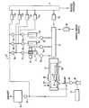
- the apparatus shown(which is generally of stainless steel) comprises a manifold 1 from which purified hydrogen is fed to mass-flow meters 2a, 2b, 2c, 2d and 2e.
- Mass-flow meter 2adirectly feeds a tubular reactor 10 with hydrogen and meters 2b, 2c and 2d feed alkyl bubblers 6b ) 6a and hydrogen telluride generator 7 via pneumatic valves 4a, 4b and 4c respectively.
- Mass-flow meter 2efeeds a bypass line 21.
- Valves 3a, 3b and 3 qmay be opened and valves 5a, 5b and 5c may be closed to turn off the associated hydrogen telluride generator 7 and alkyl bubblers 6a and 6b.
- Alkyl bubbler 6acontains dimethyl cadmium at a controlled temperature and alkyl bubbler 6b (which is similarly temperature-controlled) contains an alkyl of any suitable dopant that is required. Additionally or alternatively, dopants such as phosphorus which are conveniently available as hydrides may be added directly to the system via a mass flow controller 2f.
- Hydrogen telluride generator 7comprises a tellurium tube 9 of high purity (typical impurity levels being less than 1 part per million) in a 2450 MHz microwave cavity 8. The intensity of the microwave radiation is controlled so as to control the hydrogen telluride output, the temperature of the tellurium tube 9 remaining at approximately 25°C.
- Reactor 10is provided with a mercury bath 11 which is heated by a furnace 12 to approximately 150°C to provide a mercury atmosphere which mixes thoroughly with the reactant gases from mixer 22.
- a carbon susceptor 15is locally heated by an R.F. coil 13 and thermally decomposes the hydrogen telluride, cadmium alkyl and dopant sources (if present) in a smoothly controlled reaction to form an epitaxial layer of cadmium mercury telluride of uniform controlled composition on inclined face 14.
- a suitable substrate layersuch as cadmium telluride may be initially deposited on Surface 14 in the absence of a mercury bath. When the layer has reached a suitable thickness, it may be processed by known methods and fabricated into an infra-red photodetector device.
- a liquid coolant jacket 23prevents the reactor from overheating and condenses excess mercury vapour.
- the excess reactant gases and hydrogenare exhausted by a pump 17 and burnt (for safety reasons) after being passed over an activated charcoal bed 19.
- a cold trap 16condenses unreacted reactant gases and the pressure within the system is controlled by valves 18 and 20.
- hydrogen telluridemay be generated in situ over a tellurium tube in reactor 10, a suitable microwave cavity being provided around the reactor. Higher temperatures may then be used.
Landscapes
- Chemical & Material Sciences (AREA)
- Organic Chemistry (AREA)
- Materials Engineering (AREA)
- Inorganic Chemistry (AREA)
- Metallurgy (AREA)
- Engineering & Computer Science (AREA)
- Crystallography & Structural Chemistry (AREA)
- Chemical Kinetics & Catalysis (AREA)
- General Chemical & Material Sciences (AREA)
- Mechanical Engineering (AREA)
- Chemical Vapour Deposition (AREA)
- Crystals, And After-Treatments Of Crystals (AREA)
- Liquid Deposition Of Substances Of Which Semiconductor Devices Are Composed (AREA)
Abstract
Description
- The present invention relates to the synthesis of hydrogen telluride and the synthesis of metal tellurides from hydrogen telluride. The invention relates particularly but not exclusively to the synthesis of binary and ternary mercury tellurides such as Hg1-xCdxTe, Hg1-xMnxTe and Hg1-x (Mn1-yCdy)x Te and to photodetectors incorporating such tellurides.
- Hitherto, such binary and ternary mercury tellurides have commonly been produced by vapour-phase epitaxial methods involving the thermal decomposition of vapourised cadmium and tellurium alkyls in the presence of mercury vapour. However tellurium alkyls only decompose at high temperatures, so that the formation of cadmium mercury telluride by vapour phase epitaxy has hitherto only been possible at temperatures greater than approximately 350°C. This is frequently disadvantageous.
- Furthermore, cadmium and tellurium alkyls form adducts in the vapour phase which decompose at a lower temperature than the decomposition temperature of either of the separate alkyls. Consequently the value of x in the formula CdxHg1-xTe is a complex function of reaction conditions when the cadmium mercury telluride is formed by pyrolysis of mixed cadmium and tellurium alkyls.
- According to one aspect of the present invention, in a controlled method of producing a metal telluride, gaseous hydrogen telluride is uniformly mixed with a gaseous source of said metal, characterised in that flows of pure gaseous hydrogen telluride and gaseous sources of metal M and mercury are mixed and the flowing mixture is thermally decomposed by a heated substrate (14) to form a layer of metal mercury telluride ( MxHg1-xTe) on said substrate.
- The gaseous source of the metal may be the metal vapour itself if the metal is sufficiently volatile,
- Otherwise volatile thermally decomposable organometallic compounds such as metal alkyls may be used- suitable volatile organometallic compounds include dimethyl cadmium, di-ethyl cadmium and hydrogen-substitute metal alkyls.
- The process should be carried out in the absence of light (which photochemically decomposes hydrogen telluride) and the hydrogen telluride should be free from traces of water, oxygen and other sources of free radicals which may initiate an explosive chain reaction. The hydrogen telluride may suitably be diluted in a suitable inert diluent such as hydrogen and should according to reports be at a partial pressure below 23 Torr at room temperature, since explosions can occur at higher partial pressures. Reference is made to the following articles (which relate to the combustion properties of hydrogen telluride) in connection with the safety aspects of the process:
- A S Yushin, RV Pekhomov, Izv. Akad, Nauk. SSSR, Ser. Khim. (12), 2801-3, 1976, (CA 86 100084). V S Mikheev, L I Nikolaev, V Ya. Verkhovskii, A S Yuskin, Izv. Akad. Nauk SSSR, Ser. Khim. (9), 2117-19, 1977 (CA 88: 25066). GP Ustyugov, E N Vigdorovich, Izv. Akad. Nank SSSR, Neorg. Mater., 5(1), 163-5, 1969 (CA 65: 91010).
- However, we have found that pure hydrogen telluride is unexpectedly kinetically stable even at temperatures as high as 250°C.
- Cadmium mercury telluride of controlled composition may be made in accordance with the present invention by providing controlled flows of the gaseous hydrogen telluride and at least one of the or each said gaseous sources, allowing said flows to mix and subsequently thermally decomposing substantially all of the flowing mixture over a heated substrate to form a layer of said metal telluride on said substrate. By this means the composition of the metal telluride can be controlled by controlling the relative flow rates of the components of the gas mixture. The composition of the metal telluride layer may be varied over its thickness by altering the relative flow rates of the components of the gas mixture. The relative flow rates may be altered continuously or discontinuously to give corresponding continuous or discontinuous variations in the composition of the layer over its thickness.
- The hydrogen telluride may be generated in situ under controlled conditions.
- The gaseous source of mercury is suitably mercury vapour and the value of x in the formula CdxHg1-xTe is suitably controlled by controlling the relative flow rates of the gaseous cadmium source (which is suitably dimethyl cadmium) and the hydrogen telluride. The mercury vapour may be in equilibrium with a hot mercury bath. The total partial pressure of the reactants is suitably between 1 and 10 Torr, which may be supplemented by a sufficient partial pressure of hydrogen or other in ert diluent to bring the total pressure up to approximately atmospheric pressure.
- The substrate may suitably be composed of carbon, in which case it may be locally heated by a microwave or R.F. source. Alternatively a substrate such as cadmium telluride, indium antimonide, silicon, gallium arsenide, spinel (Mg A12 04) or sapphire (A1203) may be used, and may be mounted on a carbon susceptor heated by a microwave or R.F. source.
- Doped cadmium mercury telluride may be grown by a method in accordance with the invention by providing a controlled flow of a thermally decomposable gaseous source of dopant which is decomposed on the hot substrate and co-deposited with the other reactants. Thus aluminium, gallium, arsenic and phosphorus dopants may be obtained from vapours of their respective trimethyl compounds and silicon and germanium dopants may be obtained from their respective hydrides. Thus photovoltaic as well as photoconductive cadmium mercury telluride layers may be grown in accordance with the invention.
- The invention includes within its scope infra-red photodetector devices (whether photovoltaic or photoconductive) incorporating cadmium mercury telluride layers grown by any of the novel methods described hereinabove.
- Suitable apparatus for generating gaseous hydrogen telluride comprises means for passing a flow of molecular hydrogen over a tellurium surface and means for generating microwave radiation at said surface so as to dissociate the flowing hydrogen. Said surface may be the interior surface of a tellurium tube and the tellurium tube may be surrounded by a microwave cavity. The frequency of the microwave radiation is not critical, but may suitably be 2,450MHz.
- The above novel apparatus is particularly suitable for generating hydrogen telluride for use in methods of making high-purity tellurides (particularly cadmium mercury telluride) in accordance with the invention because the only reactants are hydrogen and tellurium, which may both be obtained free from hydride-forming impurities. However hydrogen telluride may also be obtained by other methods involving the reaction of atomic hydrogen with tellurium - for example an electric discharge between tellurium electrodes in a hydrogen atmosphere may be used.
- Methods involving the reaction of mineral acids on metal tellurides (for example aluminium telluride) or the electrolysis of aqueous solutions using a tellurium cathode produce impure hydrogen telluride which cannot easily be purified to a sufficient extent.
- A method and apparatus in accordance with the invention will now be described by way of example with reference to the accompanying drawing, which shows apparatus for the production of cadmium mercury telluride layers suitable for photodetector applications.
- The apparatus shown (which is generally of stainless steel) comprises a manifold 1 from which purified hydrogen is fed to mass-
flow meters flow meter 2a directly feeds atubular reactor 10 with hydrogen andmeters feed )6a andalkyl bubblers 6bhydrogen telluride generator 7 viapneumatic valves flow meter 2e feeds abypass line 21. Valves 3a, 3b and 3q may be opened andvalves hydrogen telluride generator 7 andalkyl bubblers bubbler 6a contains dimethyl cadmium at a controlled temperature andalkyl bubbler 6b (which is similarly temperature-controlled) contains an alkyl of any suitable dopant that is required. Additionally or alternatively, dopants such as phosphorus which are conveniently available as hydrides may be added directly to the system via amass flow controller 2f. Hydrogen telluride generator 7 comprises a tellurium tube 9 of high purity (typical impurity levels being less than 1 part per million) in a 2450 MHz microwave cavity 8. The intensity of the microwave radiation is controlled so as to control the hydrogen telluride output, the temperature of the tellurium tube 9 remaining at approximately 25°C.- Since the temperatures of the
alkyl bubblers mixer 22. and thence toreactor 10. The partial pressure of each reactant vapour is of the order of 1 Torr,the total pressure being approximately 1 atmosphere. Reactor 10 is provided with a mercury bath 11 which is heated by afurnace 12 to approximately 150°C to provide a mercury atmosphere which mixes thoroughly with the reactant gases frommixer 22. Acarbon susceptor 15 is locally heated by an R.F.coil 13 and thermally decomposes the hydrogen telluride, cadmium alkyl and dopant sources (if present) in a smoothly controlled reaction to form an epitaxial layer of cadmium mercury telluride of uniform controlled composition oninclined face 14. A suitable substrate layer such as cadmium telluride may be initially deposited onSurface 14 in the absence of a mercury bath. When the layer has reached a suitable thickness, it may be processed by known methods and fabricated into an infra-red photodetector device.- A
liquid coolant jacket 23 prevents the reactor from overheating and condenses excess mercury vapour. The excess reactant gases and hydrogen are exhausted by a pump 17 and burnt (for safety reasons) after being passed over an activatedcharcoal bed 19. Acold trap 16 condenses unreacted reactant gases and the pressure within the system is controlled byvalves 18 and 20. - In an alternative embodiment of the invention, hydrogen telluride may be generated in situ over a tellurium tube in
reactor 10, a suitable microwave cavity being provided around the reactor. Higher temperatures may then be used.
Claims (14)
1. A controlled method of producing a metal telluride wherein gaseous hydrogen telluride is uniformly mixed with a gaseous source of said metal, characterised in that flows of pure gaseous hydrogen telluride and gaseous sources of metal M and mercury are mixed and the flowing mixture is thermally decomposed by a heated substrate (14) to form a layer of metal mercury telluride ( MxHg1-xTe) on said substrate.
2 A method according to Claim 1 wherein the partial pressure of the hydrogen telluride is between 1 and 10 Torr and the hydrogen telluride and gaseous sources of cadmium and mercury are diluted with an inert diluent gas.
3. A method according to Claim 1 or Claim 2 wherein the temperature of said substrate is below 250°C.
4. A method according to any preceding Claim wherein the relative flow rates of the hydrogen telluride and the gaseous source of metal M are varied so as to vary the composition MxHg1-xTe of the deposited telluride layer over its thickness.
5. A method according to any preceding Claim wherein said gaseous source of mercury is mercury vapour.
6. A method according to any preceding Claim wherein said metal M is cadmium and said gaseous source of the metal M is a volatile organometallic cadmium compound.
7. A method according to Claim 6 wherein said organometallic compound is a cadmium alkyl.
8. A method according to Claim 7 wherein said organometallic compound is dimethyl cadmium or diethyl cadmium.
9. A method according to any preceding Claim wherein said substrate is heated by a microwave or R.F. source.
10. A method according to any preceding Claim wherein an alkyl of aluminium, gallium, arsenic or phosphorus, or a hydride of silicon or germanium is decomposed with the hydrogen telluride at said substrate (14) to form a doped telluride layer.
11. A method according to any preceding Claim wherein the hydrogen telluride is generated by an electric discharge between tellurium electrodes in a hydrogen atmosphere.
12. A photodetector device incorporating a cadmium mercury telluride layer grown by a method according to any preceding Claim.
13. Apparatus for forming a binary or ternary mercury telluride from hydrogen telluride and gaseous sources of mercury and optionally a metal M, said apparatus comprising a reactor vessel(10) housing both a substrate (14) and a tellurium surface (9), means (3d,4c,5a) for flowing hydrogen across said surface, a microwave cavity (8) surrounding at least part of said reactor vessel and arranged to dissociate hydrogen at said surface and thereby generate hydrogen telluride, and means (13) for heating said substrate to decompose the hydrogen telluride and gaseous source mercury and said metal M (if present) and form a telluride layer on said substrate.
14. A controlled method of making mercury telluride wherein gaseous hydrogen telluride is uniformly mixed with a gaseous source of mercury and the mixture is thermally decomposed by a hot substrate to form a layer of mercury telluride on said substrate.
Applications Claiming Priority (2)
| Application Number | Priority Date | Filing Date | Title |
|---|---|---|---|
| GB8327994 | 1983-10-19 | ||
| GB8327994 | 1983-10-19 |
Publications (2)
| Publication Number | Publication Date |
|---|---|
| EP0140625A1true EP0140625A1 (en) | 1985-05-08 |
| EP0140625B1 EP0140625B1 (en) | 1988-06-08 |
Family
ID=10550449
Family Applications (1)
| Application Number | Title | Priority Date | Filing Date |
|---|---|---|---|
| EP84306997AExpiredEP0140625B1 (en) | 1983-10-19 | 1984-10-10 | Tellurides |
Country Status (6)
| Country | Link |
|---|---|
| EP (1) | EP0140625B1 (en) |
| JP (1) | JPS60169563A (en) |
| DE (1) | DE3471918D1 (en) |
| DK (1) | DK501084A (en) |
| GB (1) | GB2148945B (en) |
| NO (1) | NO844142L (en) |
Cited By (4)
| Publication number | Priority date | Publication date | Assignee | Title |
|---|---|---|---|---|
| EP0288108A1 (en)* | 1987-04-16 | 1988-10-26 | Philips Electronics Uk Limited | Electronic device manufacture |
| WO1989001988A1 (en)* | 1987-08-31 | 1989-03-09 | Santa Barbara Research Center | In-situ generation of volatile compounds for chemical vapor deposition |
| US4885067A (en)* | 1987-08-31 | 1989-12-05 | Santa Barbara Research Center | In-situ generation of volatile compounds for chemical vapor deposition |
| US8377341B2 (en) | 2007-04-24 | 2013-02-19 | Air Products And Chemicals, Inc. | Tellurium (Te) precursors for making phase change memory materials |
Families Citing this family (1)
| Publication number | Priority date | Publication date | Assignee | Title |
|---|---|---|---|---|
| US7960205B2 (en) | 2007-11-27 | 2011-06-14 | Air Products And Chemicals, Inc. | Tellurium precursors for GST films in an ALD or CVD process |
Citations (8)
| Publication number | Priority date | Publication date | Assignee | Title |
|---|---|---|---|---|
| US2671739A (en)* | 1949-06-22 | 1954-03-09 | Bell Telephone Labor Inc | Plating with sulfides, selenides, and tellurides of chromium, molybdenum, and tungsten |
| GB859588A (en)* | 1957-09-03 | 1961-01-25 | Nat Res Dev | Photosensitive cells, radiation filters and semiconductor materials for use in such cells and filters |
| DE976126C (en)* | 1951-01-24 | 1963-04-04 | Walter Dr Gieseke | Method and device for the production of crystalline metal sulfides, selenides or tellurides with semiconductor properties |
| US3451845A (en)* | 1965-07-09 | 1969-06-24 | Ibm | Method for producing thin films of rare earth chalcogenides |
| US3657006A (en)* | 1969-11-06 | 1972-04-18 | Peter D Fisher | Method and apparatus for depositing doped and undoped glassy chalcogenide films at substantially atmospheric pressure |
| US3761308A (en)* | 1971-11-22 | 1973-09-25 | Ibm | Preparation of photoconductive films |
| US3808035A (en)* | 1970-12-09 | 1974-04-30 | M Stelter | Deposition of single or multiple layers on substrates from dilute gas sweep to produce optical components, electro-optical components, and the like |
| GB2078695A (en)* | 1980-05-27 | 1982-01-13 | Secr Defence | Cadmium Mercury Telluride Deposition |
Family Cites Families (1)
| Publication number | Priority date | Publication date | Assignee | Title |
|---|---|---|---|---|
| US3664866A (en)* | 1970-04-08 | 1972-05-23 | North American Rockwell | Composite, method for growth of ii{11 {14 vi{11 {0 compounds on substrates, and process for making composition for the compounds |
- 1984
- 1984-10-10GBGB08425592Apatent/GB2148945B/ennot_activeExpired
- 1984-10-10EPEP84306997Apatent/EP0140625B1/ennot_activeExpired
- 1984-10-10DEDE8484306997Tpatent/DE3471918D1/ennot_activeExpired
- 1984-10-17NONO844142Apatent/NO844142L/enunknown
- 1984-10-19JPJP59221106Apatent/JPS60169563A/enactivePending
- 1984-10-19DKDK501084Apatent/DK501084A/ennot_activeApplication Discontinuation
Patent Citations (8)
| Publication number | Priority date | Publication date | Assignee | Title |
|---|---|---|---|---|
| US2671739A (en)* | 1949-06-22 | 1954-03-09 | Bell Telephone Labor Inc | Plating with sulfides, selenides, and tellurides of chromium, molybdenum, and tungsten |
| DE976126C (en)* | 1951-01-24 | 1963-04-04 | Walter Dr Gieseke | Method and device for the production of crystalline metal sulfides, selenides or tellurides with semiconductor properties |
| GB859588A (en)* | 1957-09-03 | 1961-01-25 | Nat Res Dev | Photosensitive cells, radiation filters and semiconductor materials for use in such cells and filters |
| US3451845A (en)* | 1965-07-09 | 1969-06-24 | Ibm | Method for producing thin films of rare earth chalcogenides |
| US3657006A (en)* | 1969-11-06 | 1972-04-18 | Peter D Fisher | Method and apparatus for depositing doped and undoped glassy chalcogenide films at substantially atmospheric pressure |
| US3808035A (en)* | 1970-12-09 | 1974-04-30 | M Stelter | Deposition of single or multiple layers on substrates from dilute gas sweep to produce optical components, electro-optical components, and the like |
| US3761308A (en)* | 1971-11-22 | 1973-09-25 | Ibm | Preparation of photoconductive films |
| GB2078695A (en)* | 1980-05-27 | 1982-01-13 | Secr Defence | Cadmium Mercury Telluride Deposition |
Non-Patent Citations (2)
| Title |
|---|
| CHEMICAL ABSTRACTS, vol. 74, no. 10, March 1971, pages 97-98, no. 43957n, Columbus, Ohio, USA; & SU - A - 278 646 (OBOLONCHIK et al.) 21-08-1970* |
| JOURNAL OF THE ELECTROCHEMICAL SOCIETY, vol. 118, no. 4, April 1971, pages 644-647, The Electrochemical Society Inc., Princeton, N.J., USA; H.M. MANASEVIT et al.: "The use of metal-organics in the preparation of semiconductor materials"* |
Cited By (5)
| Publication number | Priority date | Publication date | Assignee | Title |
|---|---|---|---|---|
| EP0288108A1 (en)* | 1987-04-16 | 1988-10-26 | Philips Electronics Uk Limited | Electronic device manufacture |
| US4874634A (en)* | 1987-04-16 | 1989-10-17 | U.S. Philips Corp. | Vapor phase deposition of cadmium and mercury telluride for electronic device manufacture |
| WO1989001988A1 (en)* | 1987-08-31 | 1989-03-09 | Santa Barbara Research Center | In-situ generation of volatile compounds for chemical vapor deposition |
| US4885067A (en)* | 1987-08-31 | 1989-12-05 | Santa Barbara Research Center | In-situ generation of volatile compounds for chemical vapor deposition |
| US8377341B2 (en) | 2007-04-24 | 2013-02-19 | Air Products And Chemicals, Inc. | Tellurium (Te) precursors for making phase change memory materials |
Also Published As
| Publication number | Publication date |
|---|---|
| EP0140625B1 (en) | 1988-06-08 |
| DE3471918D1 (en) | 1988-07-14 |
| JPS60169563A (en) | 1985-09-03 |
| GB2148945A (en) | 1985-06-05 |
| GB2148945B (en) | 1987-01-07 |
| GB8425592D0 (en) | 1984-11-14 |
| NO844142L (en) | 1985-04-22 |
| DK501084A (en) | 1985-04-20 |
| DK501084D0 (en) | 1984-10-19 |
Similar Documents
| Publication | Publication Date | Title |
|---|---|---|
| US10988858B2 (en) | Method for depositing a crystal layer at low temperatures, in particular a photoluminescent IV-IV layer on an IV substrate, and an optoelectronic component having such a layer | |
| US7238596B2 (en) | Method for preparing Ge1-x-ySnxEy (E=P, As, Sb) semiconductors and related Si-Ge-Sn-E and Si-Ge-E analogs | |
| Chen et al. | MOVPE growth of InP using isobutylphosphine and tert-butylphosphine | |
| Parikh et al. | An overview of gallium nitride growth chemistry and its effect on reactor design: Application to a planetary radial-flow CVD system | |
| US5124278A (en) | Amino replacements for arsine, antimony and phosphine | |
| US4368098A (en) | Epitaxial composite and method of making | |
| EP0586321A2 (en) | Supersaturated rare earth doped semiconductor layers by CVD | |
| US4904616A (en) | Method of depositing arsine, antimony and phosphine substitutes | |
| US3382113A (en) | Method of epitaxially growing silicon carbide by pyrolytically decomposing sih4 and ch4 | |
| US4988640A (en) | Method of doping and implanting using arsine, antimony, and phosphine substitutes | |
| US4800173A (en) | Process for preparing Si or Ge epitaxial film using fluorine oxidant | |
| JPH06252057A (en) | Manufacture of semiconductor device | |
| US3338761A (en) | Method and apparatus for making compound materials | |
| US4774195A (en) | Process for the manufacture of semiconductor layers on semiconductor bodies or for the diffusion of impurities from compounds into semiconductor bodies utilizing an additional generation of activated hydrogen | |
| EP0140625A1 (en) | Tellurides | |
| KR20030095166A (en) | Method for producing powders made of gallium nitride and apparatus for producing the same | |
| JP2020007202A (en) | Group III nitride substrate and method for producing group III nitride crystal | |
| US5036022A (en) | Metal organic vapor phase epitaxial growth of group III-V semiconductor materials | |
| EP0780887A1 (en) | Method of N-type doping a compound semiconductor layer | |
| US4895737A (en) | Metal-organic chemical vapor deposition | |
| JPH03274275A (en) | Device for forming thin film utilizing organometallic gas | |
| US20210210348A1 (en) | Method For Depositing A Crystal Layer At Low Temperatures, In Particular A Photoluminescent IV-IV Layer On An IV Substrate, And An Optoelectronic Component Having Such A Layer | |
| EP0245600B1 (en) | Process for the plasma synthesis of hydride compounds and apparatus for carrying out said process | |
| CA1322935C (en) | Branched monoalkyl group v a compounds as mocvd element sources | |
| Woelk et al. | III-Nitride multiwafer MOCVD systems for blue-green LED material |
Legal Events
| Date | Code | Title | Description |
|---|---|---|---|
| PUAI | Public reference made under article 153(3) epc to a published international application that has entered the european phase | Free format text:ORIGINAL CODE: 0009012 | |
| AK | Designated contracting states | Designated state(s):DE FR IT SE | |
| 17P | Request for examination filed | Effective date:19851101 | |
| 17Q | First examination report despatched | Effective date:19861107 | |
| D17Q | First examination report despatched (deleted) | ||
| GRAA | (expected) grant | Free format text:ORIGINAL CODE: 0009210 | |
| AK | Designated contracting states | Kind code of ref document:B1 Designated state(s):DE FR IT SE | |
| ITF | It: translation for a ep patent filed | ||
| REF | Corresponds to: | Ref document number:3471918 Country of ref document:DE Date of ref document:19880714 | |
| ET | Fr: translation filed | ||
| PGFP | Annual fee paid to national office [announced via postgrant information from national office to epo] | Ref country code:DE Payment date:19881227 Year of fee payment:5 | |
| PLBE | No opposition filed within time limit | Free format text:ORIGINAL CODE: 0009261 | |
| STAA | Information on the status of an ep patent application or granted ep patent | Free format text:STATUS: NO OPPOSITION FILED WITHIN TIME LIMIT | |
| 26N | No opposition filed | ||
| PG25 | Lapsed in a contracting state [announced via postgrant information from national office to epo] | Ref country code:SE Effective date:19891011 | |
| PG25 | Lapsed in a contracting state [announced via postgrant information from national office to epo] | Ref country code:FR Effective date:19900629 | |
| PG25 | Lapsed in a contracting state [announced via postgrant information from national office to epo] | Ref country code:DE Effective date:19900703 | |
| REG | Reference to a national code | Ref country code:FR Ref legal event code:ST | |
| EUG | Se: european patent has lapsed | Ref document number:84306997.2 Effective date:19900706 |