EP0138639B1 - Inspection method for mask pattern used in semiconductor device fabrication - Google Patents
Inspection method for mask pattern used in semiconductor device fabricationDownload PDFInfo
- Publication number
- EP0138639B1 EP0138639B1EP84401661AEP84401661AEP0138639B1EP 0138639 B1EP0138639 B1EP 0138639B1EP 84401661 AEP84401661 AEP 84401661AEP 84401661 AEP84401661 AEP 84401661AEP 0138639 B1EP0138639 B1EP 0138639B1
- Authority
- EP
- European Patent Office
- Prior art keywords
- mask pattern
- inspection method
- pattern
- sensor
- video signal
- Prior art date
- Legal status (The legal status is an assumption and is not a legal conclusion. Google has not performed a legal analysis and makes no representation as to the accuracy of the status listed.)
- Expired - Lifetime
Links
Images


Classifications
- G—PHYSICS
- G03—PHOTOGRAPHY; CINEMATOGRAPHY; ANALOGOUS TECHNIQUES USING WAVES OTHER THAN OPTICAL WAVES; ELECTROGRAPHY; HOLOGRAPHY
- G03F—PHOTOMECHANICAL PRODUCTION OF TEXTURED OR PATTERNED SURFACES, e.g. FOR PRINTING, FOR PROCESSING OF SEMICONDUCTOR DEVICES; MATERIALS THEREFOR; ORIGINALS THEREFOR; APPARATUS SPECIALLY ADAPTED THEREFOR
- G03F1/00—Originals for photomechanical production of textured or patterned surfaces, e.g., masks, photo-masks, reticles; Mask blanks or pellicles therefor; Containers specially adapted therefor; Preparation thereof
- G03F1/68—Preparation processes not covered by groups G03F1/20 - G03F1/50
- G03F1/82—Auxiliary processes, e.g. cleaning or inspecting
- G03F1/84—Inspecting
- G—PHYSICS
- G03—PHOTOGRAPHY; CINEMATOGRAPHY; ANALOGOUS TECHNIQUES USING WAVES OTHER THAN OPTICAL WAVES; ELECTROGRAPHY; HOLOGRAPHY
- G03F—PHOTOMECHANICAL PRODUCTION OF TEXTURED OR PATTERNED SURFACES, e.g. FOR PRINTING, FOR PROCESSING OF SEMICONDUCTOR DEVICES; MATERIALS THEREFOR; ORIGINALS THEREFOR; APPARATUS SPECIALLY ADAPTED THEREFOR
- G03F7/00—Photomechanical, e.g. photolithographic, production of textured or patterned surfaces, e.g. printing surfaces; Materials therefor, e.g. comprising photoresists; Apparatus specially adapted therefor
- G03F7/70—Microphotolithographic exposure; Apparatus therefor
- G03F7/70483—Information management; Active and passive control; Testing; Wafer monitoring, e.g. pattern monitoring
- G03F7/70591—Testing optical components
- H—ELECTRICITY
- H01—ELECTRIC ELEMENTS
- H01L—SEMICONDUCTOR DEVICES NOT COVERED BY CLASS H10
- H01L21/00—Processes or apparatus adapted for the manufacture or treatment of semiconductor or solid state devices or of parts thereof
- H01L21/02—Manufacture or treatment of semiconductor devices or of parts thereof
- H01L21/04—Manufacture or treatment of semiconductor devices or of parts thereof the devices having potential barriers, e.g. a PN junction, depletion layer or carrier concentration layer
- H01L21/18—Manufacture or treatment of semiconductor devices or of parts thereof the devices having potential barriers, e.g. a PN junction, depletion layer or carrier concentration layer the devices having semiconductor bodies comprising elements of Group IV of the Periodic Table or AIIIBV compounds with or without impurities, e.g. doping materials
- H01L21/30—Treatment of semiconductor bodies using processes or apparatus not provided for in groups H01L21/20 - H01L21/26
Definitions
- the present inventionrelates to an inspection method as claimed in claim 1 for a mask pattern on a photomask or a wafer used in the fabrication of a semiconductor device such as an integrated circuit (IC) or a large scale integrated circuit.
- ICintegrated circuit
- ICsemiconductor integrated circuit device
- a mother patterncalled a "reticle pattern" on the wafer.
- Oneis a way of applying a photomask
- the otheris a way to print the reticle pattern directly on the wafer.
- Fig. 1 and 2show these patterning processes in the IC fabrication; Fig.1 is for the former and Fig.2 is for the latter.
- the IC patterns of the photomaskare made at first from the reticle pattern by a step and repeat printing method, and next the IC patterns of the photomask are directly printed on the wafer.
- the reticle patternis directly printed on the wafer by a step and repeat method without applying any the photomask.
- reference numeral 100is a reticle
- 200is a photomask
- 300is a wafer.
- the reticle 100is made of a piece of silicate glass for example, on which a mother pattern is printed photographically from an original pattern.
- Reference numeral 101is the mother pattern being called a "reticle pattern" here.
- the reticle pattern 101is the mother pattern, the pattern must be made with high accuracy, therefore the size of the pattern is made so large as 5 to 10 times of actual IC size. So, the reticle pattern is printed on the photomask or the wafer by an optical system having a reduction factor of the value between 1/10 and 1/5.
- the reticle pattern 101 of the reticle 100is exposed on a photographic plate fabricated on the surface of the photomask 200 by an optical system 105 having a reduction factor of the same value between 1/10 and 1/5.
- the exposureis made by a step and repeat procedure moving the photomask 200 in X and Y directions.
- Reference numeral 201shows an individual IC pattern on the photomask 200, and its size is equal to that of an IC pattern on the wafer. Therefore, after fabricating the photomask, the photomask pattern having a plurality of the IC patterns is exposed on the surface of the wafer 300 in equal size; that is, the size of an IC pattern 301 on the wafer 300 is equal to that of the IC pattern 201 on the photomask 200.
- An arrow 205shows this direct printing without reduction or magnification.
- the reticle pattern of the reticle 100is exposed on the surface of the wafer 300 by an optical system 305 having a reduction factor between 1/10 and 1/5 for the same reason as mentioned above in respect of Fig.1.
- the exposure for the printingis also made by the step and repeat procedure similarly to the case of Fig.1 moving the wafer 300 in the X and Y directions.
- Reference numeral 301shows an individual IC pattern on the wafer 300.
- the phrase "printed pattern”will be used hereinafter to designate the printed IC patterns on the photomask 200 or the wafer 300 in Fig.1, and on the wafer 300 in Fig.2, whereas, the phrase “mask pattern” will be used to designate for the IC patterns on the photomask 200 in Fig.1, and the reticle pattern 101 on the reticle 100 in Fig.2.
- the reticle pattern itselfis made by printing an original pattern as mentioned before, the original pattern becomes a mask pattern and the reticle pattern 101 on the reticle 100 becomes a printed pattern in this case.
- the exposing process for the printingis very important in the IC patterning process, and a defect cannot be allowed to exist. However, actually it becomes necessary to pay great attention to the fact that recently the probability for incorrect printing to occur has increased because the IC pattern has become very small and complicated to increase the IC packing density.
- Fig. 3shows examples of defects in the printed patterns with reference to the manufacture of a reticle pattern.
- Fig. 3 (a)shows an original pattern of the reticle pattern
- Fig. 3 (b)shows an example of defect of the printed pattern (reticle pattern) on the reticle
- Fig. 3 (c)shows another example of the defect of the printed reticle pattern.
- the printed pattern 1001has an incorrect part 1011 which is mainly produced in a wrong developing process.
- the printed pattern 1002has a defective part 1012 which is mainly produced in a wrong exposing process.
- the defects of these kindswill occur also in the patterning process of the wafer, and in each case, the defect occurs in the exposing or printing process presupposing that the mask pattern is correct. Therefore, it can be said that the defect can be avoided so long as sufficient attention is paid to the semiconductor patterning process. However, though sufficient attention is paid, if the mask pattern itself has a defect or the dust exists near by the mask pattern, it is not possible to avoid that an abnormality appears on the printed pattern.
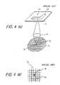
- Fig. 4illustrates this example showing the same patterning process as in Fig. 2; that is, the wafer is printed directly from the reticle pattern of the reticle.
- reference numeral 12is a reticle
- 16is a wafer
- 20is an optical system having a reduction factor of the value between 1/10 and 1/5.
- reference numeral 60is a reticle pattern
- 14is dust. If such dust 14 exists on the reticle 12, a dust pattern 141 is printed on the wafer 16 beside a correct printed pattern 18 of the mask pattern 60.
- Fig. 4 (b)shows an expanded perspective illustration of the printed pattern on the wafer 16. Though it is not shown in the figures, such dust pattern 141 is printed on all of the patterns on the wafer 16.
- the reticle pattern itselfcan be carefully inspected by various methods. Therefore, the probability that failure be caused by the defect of the reticle pattern itself can be rather low.
- the object of the present inventionis to improve the inspection method of the mask pattern so as to find out a defect of an actually exposed mask pattern caused by dust on the mask or defects of the optical system. Defects of this kind have not been able to be detected by the prior art inspection method such as a comparing method.
- Another object of the present inventionis to save time and reduce cost in the IC production.
- the present inventionis performed by applying an image sensor on the stage on which an element such as a wafer or a photomask is mounted.
- An optical image of the mask patternis projected on the image sensor which produces a video signal called a sensor video signal.
- This optical image of the mask patternis almost identical to the actually exposed pattern on the wafer.
- the sensor video signalis compared with a data video signal which is a standard video signal taken from a designating database to fabricate the mask pattern. Said steps are processed before exposing said mask pattern on said fabricating object and said exposing is processed after said mask pattern has been judged to be normal.
- Such a methodin which the almost actually exposed pattern can be inspected, permits to save a lot of time in the patterning process, especially in the event of a complicated IC pattern, and hence to reduce the cost of the IC product.
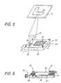
- FIG. 5illustrates a semiconductor patterning system having a reticle, an optical system, and a stage.
- reference numeral 12is a reticle
- 60is a reticle pattern on the reticle 12
- 30is a stage for mounting a wafer
- 26is a wafer
- 22is a first window opened at the surface of the stage 30, the wafer 26 being mounted in the window 22
- 24is a second window opened beside the first window 22 and in which an image sensor 28 is mounted
- 20is an optical system by which an optical image of the reticle pattern 60 is exposed and printed on the wafer 26 and also projected on the image sensor 28 switched by the operator.
- the optical system 20mainly serves to expose and print the reticle pattern 60 on the wafer 26 so that each printed IC pattern is placed in a respective block of a checked pattern 261 by moving the stage 30 sequentially.
- the optical system 20has a reduction factor between 1/10 and 1/5.
- additional functionis provided to inspect the optical image of the reticle pattern 60 before exposing it on the wafer 26. The inspection is done by projecting the optical image toward the image sensor 28 shifting the stage 30.
- This application of the image sensor 28is a point of the present invention.
- the reticle 12, the optical system 20 and the stage 30are installed in the airtight case (not shown) so that the mask pattern and wafer can be kept dust free.
- Fig. 6the same reference numerals designate the same objects as in Fig. 5, and 34 is a case of the stage, 341 is a bottom plate which supports the wafer 26 to the case 34 pushing up the wafer 26 from the bottom, and 32 is a sliding shutter to protect the wafer 26 from the exposure of the light during the inspection by the image sensor.
- Fig. 7shows a block diagram for a control system for the inspection system by the present invention.
- the reference numerals which are the same as in Fig. 5 or 6designate respectively the same objects
- 29is a stage driver which drives the stage 30 in X or Y direction (see Fig.5)
- 36is a scanning unit to switch sequentially the multi-elements of the imaging sensor 28 to convert the optical image corresponding to the multi-elements into electric signals
- 38is a stage controller which controls the scanning of the stage 30 and the scanning unit 36
- V ashows a sensor video signal which is the output signal of the image sensor 28
- 44is a first write-in unit which writes the sensor video signal V a into a first image memory 40
- 50is a magnetic tape (MT) in which the designing data to fabricate the IC pattern are stored
- 48is a video signal generator
- V bshows a data video signal
- 46is a second write-in unit
- 42is a second image memory
- 51is a
- the preparation of the exposureis done by mounting the wafer 26 on the stage 30 as shown in Fig. 6 and installing the reticle 12 as shown in Fig. 5.
- an exposing procedureis advanced; namely, the wafer 26 is brought by moving the stage so that the mask pattern 60 is exposed on a respective position of the wafer 26 by the step and repeat process, then each IC pattern is printed in each square (reference numeral 261 in Fig. 5) that corresponds to each chip of the IC as shown in Fig. 5.
- mask pattern 60is first projected on the second window 24 before beginning the exposing process on the wafer 26.
- the optical image of the reticle pattern 60 projected on the second window 24is scanned by the image sensor 28 converting to a train of video signals which is called herein a sensor video signal V a .
- the sensor video signal V ais memorized sequentially in the first image memory 40 through the first writing unit 44, and therefore, the memorized video signal includes a signal of a defect or dust if they exist on the mask pattern 60 or on the reticle 12.
- designing data of the reticle pattern 60 stored in the MT 50are read out and converted into the data video signal V b , and memorized in the second image memory 42.
- the data video signal V b stored in the second image memory 42is used as a standard signal to inspect the sensor video signal V a stored in the first image memory 40.
- Both video signals V a and V bare read out from the image memories 40 and 42 respectively and sent to the comparator 52 by the control of the read-out unit 51, and the inspection can be made by comparator 52 comparing the sensor video signal V a with the data video signal V b .
- the sensor video signal V amust be equal to the data video signal V b . If the sensor video signal V a had a defect which might be caused by failure in the patterning process for the mask pattern 60, or dust existing on the reticle 12, the comparator 52 detects the abnormality.
- the two-dimensional image sensorconsists of two-dimensional multi-elements of the sensor.
- the size of the sensoris equal to the size of a single block of the check pattern 261 in Fig. 5; it is also equal to the size of the one IC chip pattern to be printed on the wafer 26. Therefore, when the optical image of the reticle pattern 60 is projected on the image sensor, the sensor video signal V a can be provided simultaneously without scanning the stage 30.
- a one-dimensional image sensor(a line sensor) also can be applied. This sensor consists of the multi-elements arranged in a line corresponding the either side of the rectangular reticle pattern 60.
- the sensor video signal V a along the lineis simultaneously provided.
- the two-dimensional video signalcan be obtained by mechanically scanning the stage 30 in Y direction.
- Fig. 7shows the case which uses a one-dimensional image sensor.
- the sensor video signal V amust be synchronized with the scanning (switching) of the scanning unit 36 and the scanning of the stage 30, and this synchronization can be made by the scanning unit 36 and the stage driver 29 controlled by the control signals from the stage controller 38.
- optical system 20 in Fig. 5another type of optical system can be used to project the reticle pattern 60 on the image sensor 28, apart from the optical system for printing the wafer. And the optical image of the reticle pattern on the image sensor might be enlarged with respect to the exposed image on the wafer. This system is effective to satisfy the resolution of the image sensor when the mask pattern is too much complicated and requires many picture elements.
- the video signal generator 48is required to convert the form of the design data in the MT 50 into the form of the data video signal V b to compare easily the sensor video signal V a with the designing data. Because, the data stored in the MT 50 generally has a vector form, therefore, the data is required to convert to the form of the sensor video signal V a .
- the first image memory 40 and the second image memory 42each have memory cells.
- the amount of the memory cellsis defined by the amount of the picture elements of the mask pattern which is also defined by the required resolution with respect to the IC pattern. Considering the above, if the mask pattern can be divided to N lines and M picture elements per each line, the memory cells also can be arranged N lines and M cells per each line, so that the total data capacity of each image memory becomes N x M bits.
- the resolution of the optical system 20is also defined by the resolution of the IC pattern. Therefore, it is not necessary to pay attention to dust when the dust is so tiny that it can not be resolved by the optical system 20.
- the pattern checking method of the present inventionis performed right before actually exposing the printing pattern on the wafer. Therefore it is very effective to decrease the failure due to the defect of the reticle pattern. It is very effective to increase the yield and decrease the manufacturing cost of ICs. And the disclosure has been done for the IC fabrication, but it will be clear that the process can be applied to any of semiconductor device manufacturing.
- the above embodimenthas disclosed the inspection which was performed right before actually exposing the printing pattern from the reticle on the wafer, however similar effect can be obtained by applying the present invention to an optical image of the mask pattern right before exposing the mask pattern from the reticle on the photomask and right before exposing the mask pattern from the photomask on the wafer.
Landscapes
- Physics & Mathematics (AREA)
- General Physics & Mathematics (AREA)
- Engineering & Computer Science (AREA)
- Condensed Matter Physics & Semiconductors (AREA)
- Manufacturing & Machinery (AREA)
- Computer Hardware Design (AREA)
- Microelectronics & Electronic Packaging (AREA)
- Power Engineering (AREA)
- Investigating Materials By The Use Of Optical Means Adapted For Particular Applications (AREA)
- Exposure And Positioning Against Photoresist Photosensitive Materials (AREA)
- Testing Or Measuring Of Semiconductors Or The Like (AREA)
- Preparing Plates And Mask In Photomechanical Process (AREA)
- Exposure Of Semiconductors, Excluding Electron Or Ion Beam Exposure (AREA)
Description
- The present invention relates to an inspection method as claimed in claim 1 for a mask pattern on a photomask or a wafer used in the fabrication of a semiconductor device such as an integrated circuit (IC) or a large scale integrated circuit.
- For the sake of convenience, the short word "IC" will be used as a "semiconductor integrated circuit device" in this disclosure hereinafter.
- In the IC patterning process, there are two ways to print a mother pattern called a "reticle pattern" on the wafer. One is a way of applying a photomask, and the other is a way to print the reticle pattern directly on the wafer. Fig. 1 and 2 show these patterning processes in the IC fabrication; Fig.1 is for the former and Fig.2 is for the latter. In the way of Fig.1, the IC patterns of the photomask are made at first from the reticle pattern by a step and repeat printing method, and next the IC patterns of the photomask are directly printed on the wafer. On the other hand, in the way of Fig.2, the reticle pattern is directly printed on the wafer by a step and repeat method without applying any the photomask.
- In Fig. 1 and 2,
reference numeral 100 is a reticle, 200 is a photomask, and 300 is a wafer. Thereticle 100 is made of a piece of silicate glass for example, on which a mother pattern is printed photographically from an original pattern.Reference numeral 101 is the mother pattern being called a "reticle pattern" here. As thereticle pattern 101 is the mother pattern, the pattern must be made with high accuracy, therefore the size of the pattern is made so large as 5 to 10 times of actual IC size. So, the reticle pattern is printed on the photomask or the wafer by an optical system having a reduction factor of the value between 1/10 and 1/5. - In Fig. 1, the
reticle pattern 101 of thereticle 100 is exposed on a photographic plate fabricated on the surface of thephotomask 200 by anoptical system 105 having a reduction factor of the same value between 1/10 and 1/5. The exposure is made by a step and repeat procedure moving thephotomask 200 in X and Y directions.Reference numeral 201 shows an individual IC pattern on thephotomask 200, and its size is equal to that of an IC pattern on the wafer. Therefore, after fabricating the photomask, the photomask pattern having a plurality of the IC patterns is exposed on the surface of thewafer 300 in equal size; that is, the size of anIC pattern 301 on thewafer 300 is equal to that of theIC pattern 201 on thephotomask 200. Anarrow 205 shows this direct printing without reduction or magnification. - In Fig. 2, the reticle pattern of the
reticle 100 is exposed on the surface of thewafer 300 by anoptical system 305 having a reduction factor between 1/10 and 1/5 for the same reason as mentioned above in respect of Fig.1. The exposure for the printing is also made by the step and repeat procedure similarly to the case of Fig.1 moving thewafer 300 in the X and Y directions.Reference numeral 301 shows an individual IC pattern on thewafer 300. - The phrase "printed pattern" will be used hereinafter to designate the printed IC patterns on the
photomask 200 or thewafer 300 in Fig.1, and on thewafer 300 in Fig.2, whereas, the phrase "mask pattern" will be used to designate for the IC patterns on thephotomask 200 in Fig.1, and thereticle pattern 101 on thereticle 100 in Fig.2. Similarly, as the reticle pattern itself is made by printing an original pattern as mentioned before, the original pattern becomes a mask pattern and thereticle pattern 101 on thereticle 100 becomes a printed pattern in this case. - The exposing process for the printing is very important in the IC patterning process, and a defect cannot be allowed to exist. However, actually it becomes necessary to pay great attention to the fact that recently the probability for incorrect printing to occur has increased because the IC pattern has become very small and complicated to increase the IC packing density.
- Fig. 3 shows examples of defects in the printed patterns with reference to the manufacture of a reticle pattern. Fig. 3 (a) shows an original pattern of the reticle pattern, Fig. 3 (b) shows an example of defect of the printed pattern (reticle pattern) on the reticle, and Fig. 3 (c) shows another example of the defect of the printed reticle pattern. In Fig. 3 (b), the printed
pattern 1001 has anincorrect part 1011 which is mainly produced in a wrong developing process. In Fig. 3 (c), the printedpattern 1002 has adefective part 1012 which is mainly produced in a wrong exposing process. - The defects of these kinds will occur also in the patterning process of the wafer, and in each case, the defect occurs in the exposing or printing process presupposing that the mask pattern is correct. Therefore, it can be said that the defect can be avoided so long as sufficient attention is paid to the semiconductor patterning process. However, though sufficient attention is paid, if the mask pattern itself has a defect or the dust exists near by the mask pattern, it is not possible to avoid that an abnormality appears on the printed pattern.
- Fig. 4 illustrates this example showing the same patterning process as in Fig. 2; that is, the wafer is printed directly from the reticle pattern of the reticle. In the figure,
reference numeral 12 is a reticle, 16 is a wafer, and 20 is an optical system having a reduction factor of the value between 1/10 and 1/5. On thereticle 12,reference numeral 60 is a reticle pattern, and 14 is dust. Ifsuch dust 14 exists on thereticle 12, adust pattern 141 is printed on thewafer 16 beside a correct printedpattern 18 of themask pattern 60. Fig. 4 (b) shows an expanded perspective illustration of the printed pattern on thewafer 16. Though it is not shown in the figures,such dust pattern 141 is printed on all of the patterns on thewafer 16. - If dust exists with the mask pattern or if a mask pattern itself has a defect, the whole patterning process ends in a failure. If such trouble occurs, the IC product suffers damage though every later process is correct. This gives great influence on the IC cost, because the IC patterning process also becomes more complicated as the packing density increases. So, the cause of the defect must be found out and removed as quickly as possible in the early stage of the patterning process.
- Usually, the reticle pattern itself can be carefully inspected by various methods. Therefore, the probability that failure be caused by the defect of the reticle pattern itself can be rather low.
- However, when the reticle pattern, which has been inspected and judged that it had no defect, is printed on the wafer, still the following problems are possible to occur.
- Firstly, when the reticle is mounted on a projecting system as shown by the
reticle 12 in Fig.4(a) and dust happens to be stuck on the reticle, the image of the dust must be printed. Secondly, when the optical system has some defect, the reticle pattern cannot be correctly printed on the wafer. - Thus, though the reticle pattern itself is perfect, the above problems produced after the reticle inspection cause a defect to the actual optical image of the reticle pattern projected on the wafer, and the optical image has not been detected by the prior art reticle inspection.
- Therefore, the object of the present invention is to improve the inspection method of the mask pattern so as to find out a defect of an actually exposed mask pattern caused by dust on the mask or defects of the optical system. Defects of this kind have not been able to be detected by the prior art inspection method such as a comparing method. Another object of the present invention is to save time and reduce cost in the IC production.
- The present invention is performed by applying an image sensor on the stage on which an element such as a wafer or a photomask is mounted. An optical image of the mask pattern is projected on the image sensor which produces a video signal called a sensor video signal. This optical image of the mask pattern is almost identical to the actually exposed pattern on the wafer. Then, in order to judge whether the mask pattern is normal, the sensor video signal is compared with a data video signal which is a standard video signal taken from a designating database to fabricate the mask pattern. Said steps are processed before exposing said mask pattern on said fabricating object and said exposing is processed after said mask pattern has been judged to be normal.
- Such a method, in which the almost actually exposed pattern can be inspected, permits to save a lot of time in the patterning process, especially in the event of a complicated IC pattern, and hence to reduce the cost of the IC product.
- Fig. 1 is a perspective illustration showing a principle of a patterning process for semiconductor devices;
- Fig. 2 is a perspective illustration showing a principle of another patterning process;
- Fig. 3 shows an example of an original pattern and some kinds of defects on the printed pattern of the original pattern;
- Fig. 3 (a) shows an example of the original pattern for the reticle mask pattern;
- Fig. 3 (b) shows an example of a defect on the printed pattern of the original reticle pattern;
- Fig. 3 (c) shows another example of a defect on the printed pattern of the original reticle pattern;
- Fig. 4 shows a prior art fabrication system for semiconductor devices and the detail of the printed pattern in the system;
- Fig. 4 (a) is a perspective illustration showing a semiconductor fabricating system having a reticle, an optical system, and a wafer;
- Fig. 4 (b) shows a partially expanded view of the printed pattern;
- Fig. 5 is a perspective illustration showing an embodiment of the present invention for a semiconductor fabricating system which includes an inspecting system;
- Fig. 6 is a sectional view of a stage at A - A shown in Fig. 5; and
- Fig. 7 is a block diagram of an inspecting system embodying the present invention relating to Fig. 5 and 6.
- A preferred embodiment for the present invention will be disclosed with regard to Figs. 5, 6, and 7. The inspecting object of the present invention is a mask pattern, so it can be applied to any case as shown in Fig. 1 or 2. In this embodiment, the case of Fig. 2 will be disclosed; that is, the reticle pattern is printed directly on the wafer. Fig. 5 illustrates a semiconductor patterning system having a reticle, an optical system, and a stage.
- In Fig. 5,
reference numeral 12 is a reticle, 60 is a reticle pattern on thereticle stage 30, thewafer 26 being mounted in thewindow first window 22 and in which animage sensor 28 is mounted, and 20 is an optical system by which an optical image of thereticle pattern 60 is exposed and printed on thewafer 26 and also projected on theimage sensor 28 switched by the operator. Theoptical system 20 mainly serves to expose and print thereticle pattern 60 on thewafer 26 so that each printed IC pattern is placed in a respective block of a checkedpattern 261 by moving thestage 30 sequentially. Usually theoptical system 20 has a reduction factor between 1/10 and 1/5. In this system, additional function is provided to inspect the optical image of thereticle pattern 60 before exposing it on thewafer 26. The inspection is done by projecting the optical image toward theimage sensor 28 shifting thestage 30. This application of theimage sensor 28 is a point of the present invention. Thereticle 12, theoptical system 20 and thestage 30 are installed in the airtight case (not shown) so that the mask pattern and wafer can be kept dust free. - In Fig. 6, the same reference numerals designate the same objects as in Fig. 5, and 34 is a case of the stage, 341 is a bottom plate which supports the
wafer 26 to thecase 34 pushing up thewafer 26 from the bottom, and 32 is a sliding shutter to protect thewafer 26 from the exposure of the light during the inspection by the image sensor. - Fig. 7 shows a block diagram for a control system for the inspection system by the present invention. In the figure, the reference numerals which are the same as in Fig. 5 or 6 designate respectively the same objects, and 29 is a stage driver which drives the
stage 30 in X or Y direction (see Fig.5), 36 is a scanning unit to switch sequentially the multi-elements of theimaging sensor 28 to convert the optical image corresponding to the multi-elements into electric signals, 38 is a stage controller which controls the scanning of thestage 30 and thescanning unit 36, Va shows a sensor video signal which is the output signal of theimage sensor first image memory first memory 40 and thesecond memory 42 to read out the memorized signal and send it to acomparator - The operation of the embodiment is as follows. At first, the preparation of the exposure is done by mounting the
wafer 26 on thestage 30 as shown in Fig. 6 and installing thereticle 12 as shown in Fig. 5. When the preparation has been made, in the operation of the prior art inspection, an exposing procedure is advanced; namely, thewafer 26 is brought by moving the stage so that themask pattern 60 is exposed on a respective position of thewafer 26 by the step and repeat process, then each IC pattern is printed in each square (reference numeral 261 in Fig. 5) that corresponds to each chip of the IC as shown in Fig. 5. However, in the present invention,mask pattern 60 is first projected on thesecond window 24 before beginning the exposing process on thewafer 26. The optical image of thereticle pattern 60 projected on thesecond window 24 is scanned by theimage sensor 28 converting to a train of video signals which is called herein a sensor video signal Va. The sensor video signal Va is memorized sequentially in thefirst image memory 40 through thefirst writing unit 44, and therefore, the memorized video signal includes a signal of a defect or dust if they exist on themask pattern 60 or on thereticle 12. - At the same time, designing data of the
reticle pattern 60 stored in theMT 50 are read out and converted into the data video signal Vb, and memorized in thesecond image memory 42. The data video signal Vb stored in thesecond image memory 42 is used as a standard signal to inspect the sensor video signal Va stored in thefirst image memory 40. Both video signals Va and Vb are read out from theimage memories comparator 52 by the control of the read-outunit 51, and the inspection can be made bycomparator 52 comparing the sensor video signal Va with the data video signal Vb. As themask pattern 60 was made by an original pattern which was made by the design data, the sensor video signal Va must be equal to the data video signal Vb. If the sensor video signal Va had a defect which might be caused by failure in the patterning process for themask pattern 60, or dust existing on thereticle 12, thecomparator 52 detects the abnormality. - There are several possible kinds of
image sensor 28. For example, a two-dimensional image sensor is applicable as the image sensor. The two-dimensional image sensor consists of two-dimensional multi-elements of the sensor. In this case, the size of the sensor is equal to the size of a single block of thecheck pattern 261 in Fig. 5; it is also equal to the size of the one IC chip pattern to be printed on thewafer 26. Therefore, when the optical image of thereticle pattern 60 is projected on the image sensor, the sensor video signal Va can be provided simultaneously without scanning thestage 30. Instead of this, a one-dimensional image sensor (a line sensor) also can be applied. This sensor consists of the multi-elements arranged in a line corresponding the either side of therectangular reticle pattern 60. The sensor video signal Va along the line is simultaneously provided. For example, if the direction of the sensors is aligned in X direction, the two-dimensional video signal can be obtained by mechanically scanning thestage 30 in Y direction. Fig. 7 shows the case which uses a one-dimensional image sensor. In this case, the sensor video signal Va must be synchronized with the scanning (switching) of thescanning unit 36 and the scanning of thestage 30, and this synchronization can be made by thescanning unit 36 and thestage driver 29 controlled by the control signals from thestage controller 38. - Further, instead of the
optical system 20 in Fig. 5, another type of optical system can be used to project thereticle pattern 60 on theimage sensor 28, apart from the optical system for printing the wafer. And the optical image of the reticle pattern on the image sensor might be enlarged with respect to the exposed image on the wafer. This system is effective to satisfy the resolution of the image sensor when the mask pattern is too much complicated and requires many picture elements. - The
video signal generator 48 is required to convert the form of the design data in theMT 50 into the form of the data video signal Vb to compare easily the sensor video signal Va with the designing data. Because, the data stored in theMT 50 generally has a vector form, therefore, the data is required to convert to the form of the sensor video signal Va. - The
first image memory 40 and thesecond image memory 42 each have memory cells. The amount of the memory cells is defined by the amount of the picture elements of the mask pattern which is also defined by the required resolution with respect to the IC pattern. Considering the above, if the mask pattern can be divided to N lines and M picture elements per each line, the memory cells also can be arranged N lines and M cells per each line, so that the total data capacity of each image memory becomes N x M bits. - The resolution of the
optical system 20 is also defined by the resolution of the IC pattern. Therefore, it is not necessary to pay attention to dust when the dust is so tiny that it can not be resolved by theoptical system 20. - In the above disclosure the description has been done with respect to the case of printing the reticle pattern directly on the wafer, but it will be clear that the process described above can be applied to the case using a photomask.
- In any case the pattern checking method of the present invention is performed right before actually exposing the printing pattern on the wafer. Therefore it is very effective to decrease the failure due to the defect of the reticle pattern. It is very effective to increase the yield and decrease the manufacturing cost of ICs. And the disclosure has been done for the IC fabrication, but it will be clear that the process can be applied to any of semiconductor device manufacturing.
- The above embodiment has disclosed the inspection which was performed right before actually exposing the printing pattern from the reticle on the wafer, however similar effect can be obtained by applying the present invention to an optical image of the mask pattern right before exposing the mask pattern from the reticle on the photomask and right before exposing the mask pattern from the photomask on the wafer.
Claims (14)
- An inspection method for a mask pattern used in a semiconductor fabrication applying an optical system (20) by which said mask pattern (60) is exposed on a fabricating object to print said mask pattern, characterized in that it comprises the steps of:
projecting an optical image of said mask pattern (60) on an image sensor (28) provided on a stage (30) on which said fabricating object (26) is mounted, said image sensor (28) converting said optical image to a sensor video signal (Va); and
judging whether said mask pattern is normal by comparing said sensor video signal (Va) with a data video signal (Vb) taken from designating data having been used in fabricating said mask pattern (60),
and that said steps are processed before exposing said mask pattern (60) on said fabricating object (26) and said exposing is processed after said mask pattern has been judged to be normal. - The inspection method according to claim 1, characterized in that said mask pattern comprises a mask pattern (60) on a reticle (12).
- The inspection method according to claim 1, characterized in that said mask pattern comprises a single pattern (60).
- The inspection method according to claim 3, characterized in that said single mask pattern (60) comprises the mask pattern on a reticle (12).
- The inspection method according to claim 1, characterized in that said mask pattern comprises a plurality of patterns each having a same shape and size.
- The inspection method according to claim 5, characterized in that said plurality of said mask patterns comprise the reticle patterns on a reticle.
- The inspection method according to claim 1, characterized in that said fabricating object comprises a semiconductor wafer (26) to be fabricated.
- The inspection method according to claim 1, characterized in that said fabricating object comprises a photomask (200) to be fabricated.
- The inspection method according to claim 1, characterized in that said optical system comprises a single optical system (20) by which said optical image of said mask pattern is projected on either said fabricating object (26) or said image sensor (28) by means of a reducing projection.
- The inspection method according to claim 1, characterized in that said optical system comprises different optical systems: one being for said fabricating object and the other being for said image sensor.
- The inspection method according to claim 10, characterized in that said optical system for said image sensor comprises a means for having smaller reduction factor than a reduction factor of said optical system for said fabricating object.
- The inspection method according to claim 1, characterized in that said image sensor (28) comprises a two-dimensional image sensor having a plurality of sensor elements arranged in a whole image plane which simultaneously converts said optical image of said mask pattern to said sensor video signal (Va).
- The inspection method according to claim 1, characterized in that said image sensor (28) comprises a one-dimensional image sensor having a plurality of sensor elements arranged on a line parallel to one side of said optical image of said mask pattern, which converts said optical image of said mask pattern to said sensor video signal (Va) by mechanically scanning said stage (30) in a lateral direction to the line of sensor arrangement.
- The inspection method according to claim 1, characterized in that a comparator (52) is used to compare said sensor video signal (Va) and said data video signal (Vb) by reading out the data of a first image memory (40) in which the data of said sensor video signal (Va) are written and the data of a second image memory (42) in which the data of said data video signal (Vb) are written.
Applications Claiming Priority (2)
| Application Number | Priority Date | Filing Date | Title |
|---|---|---|---|
| JP170796/83 | 1983-09-16 | ||
| JP58170796AJPS6062122A (en) | 1983-09-16 | 1983-09-16 | Mask pattern exposure method |
Publications (3)
| Publication Number | Publication Date |
|---|---|
| EP0138639A2 EP0138639A2 (en) | 1985-04-24 |
| EP0138639A3 EP0138639A3 (en) | 1987-11-25 |
| EP0138639B1true EP0138639B1 (en) | 1992-01-22 |
Family
ID=15911507
Family Applications (1)
| Application Number | Title | Priority Date | Filing Date |
|---|---|---|---|
| EP84401661AExpired - LifetimeEP0138639B1 (en) | 1983-09-16 | 1984-08-13 | Inspection method for mask pattern used in semiconductor device fabrication |
Country Status (5)
| Country | Link |
|---|---|
| US (1) | US4641353A (en) |
| EP (1) | EP0138639B1 (en) |
| JP (1) | JPS6062122A (en) |
| KR (1) | KR890003145B1 (en) |
| DE (1) | DE3485474D1 (en) |
Families Citing this family (57)
| Publication number | Priority date | Publication date | Assignee | Title |
|---|---|---|---|---|
| JPS60235136A (en)* | 1984-05-09 | 1985-11-21 | Kyodo Printing Co Ltd | Plate checking method |
| GB8610655D0 (en)* | 1986-05-01 | 1986-06-04 | Smiths Industries Plc | Integrated circuit substrates |
| GB2190215B (en)* | 1986-05-01 | 1989-12-13 | Smiths Industries Plc | Integrated circuit substrates and masks |
| JPS62263646A (en)* | 1986-05-12 | 1987-11-16 | Toshiba Corp | Wafer inspection equipment |
| US4734923A (en)* | 1986-05-19 | 1988-03-29 | Hampshire Instruments, Inc | Lithographic system mask inspection device |
| US4809341A (en)* | 1986-07-18 | 1989-02-28 | Fujitsu Limited | Test method and apparatus for a reticle or mask pattern used in semiconductor device fabrication |
| CA1242815A (en)* | 1987-03-20 | 1988-10-04 | Pak K. Leung | Defect detection method of semiconductor wafer patterns |
| US4758094A (en)* | 1987-05-15 | 1988-07-19 | Kla Instruments Corp. | Process and apparatus for in-situ qualification of master patterns used in patterning systems |
| US5014326A (en)* | 1989-03-03 | 1991-05-07 | Greyhawk Systems, Inc. | Projected image linewidth correction apparatus and method |
| GB9021444D0 (en)* | 1990-10-02 | 1990-11-14 | Delco Electronic Overseas Corp | Light mask |
| JP2667940B2 (en)* | 1992-04-27 | 1997-10-27 | 三菱電機株式会社 | Mask inspection method and mask detection device |
| US5795688A (en)* | 1996-08-14 | 1998-08-18 | Micron Technology, Inc. | Process for detecting defects in photomasks through aerial image comparisons |
| US6091845A (en)* | 1998-02-24 | 2000-07-18 | Micron Technology, Inc. | Inspection technique of photomask |
| US6297879B1 (en)* | 1998-02-27 | 2001-10-02 | Micron Technology, Inc. | Inspection method and apparatus for detecting defects on photomasks |
| US6466314B1 (en)* | 1998-09-17 | 2002-10-15 | Applied Materials, Inc. | Reticle design inspection system |
| US6625800B1 (en) | 1999-12-30 | 2003-09-23 | Intel Corporation | Method and apparatus for physical image based inspection system |
| AU2002353466A1 (en)* | 2002-11-21 | 2004-06-15 | Xtend Networks Ltd. | Apparatus, system and method for the transmission of a dymatic bandwidth signal across a catv network |
| US6950183B2 (en)* | 2003-02-20 | 2005-09-27 | International Business Machines Corporation | Apparatus and method for inspection of photolithographic mask |
| JP4091605B2 (en)* | 2003-03-31 | 2008-05-28 | 富士通株式会社 | Photomask pattern inspection method, photomask pattern inspection apparatus, and photomask pattern inspection program |
| US7221788B2 (en)* | 2003-07-01 | 2007-05-22 | Infineon Technologies Ag | Method of inspecting a mask or reticle for detecting a defect, and mask or reticle inspection system |
| US7271891B1 (en)* | 2003-08-29 | 2007-09-18 | Kla-Tencor Technologies Corporation | Apparatus and methods for providing selective defect sensitivity |
| KR101056142B1 (en)* | 2004-01-29 | 2011-08-10 | 케이엘에이-텐코 코포레이션 | Computerized method for detecting defects in reticle design data |
| JP4125273B2 (en)* | 2004-08-24 | 2008-07-30 | キヤノン株式会社 | Image processing apparatus and method, and program |
| JP4904034B2 (en)* | 2004-09-14 | 2012-03-28 | ケーエルエー−テンカー コーポレイション | Method, system and carrier medium for evaluating reticle layout data |
| DE102005032601A1 (en)* | 2005-01-07 | 2006-07-20 | Heidelberger Druckmaschinen Ag | press |
| JP4664688B2 (en)* | 2005-01-14 | 2011-04-06 | 東芝メモリシステムズ株式会社 | Manufacturing method of industrial products |
| US7769225B2 (en) | 2005-08-02 | 2010-08-03 | Kla-Tencor Technologies Corp. | Methods and systems for detecting defects in a reticle design pattern |
| US7676077B2 (en)* | 2005-11-18 | 2010-03-09 | Kla-Tencor Technologies Corp. | Methods and systems for utilizing design data in combination with inspection data |
| US8041103B2 (en)* | 2005-11-18 | 2011-10-18 | Kla-Tencor Technologies Corp. | Methods and systems for determining a position of inspection data in design data space |
| US7570796B2 (en)* | 2005-11-18 | 2009-08-04 | Kla-Tencor Technologies Corp. | Methods and systems for utilizing design data in combination with inspection data |
| JP2007142275A (en)* | 2005-11-21 | 2007-06-07 | Toshiba Corp | Photomask determination method, semiconductor device manufacturing method, and program |
| JP5427609B2 (en) | 2006-12-19 | 2014-02-26 | ケーエルエー−テンカー・コーポレーション | Inspection recipe creation system and method |
| US8194968B2 (en)* | 2007-01-05 | 2012-06-05 | Kla-Tencor Corp. | Methods and systems for using electrical information for a device being fabricated on a wafer to perform one or more defect-related functions |
| US7738093B2 (en)* | 2007-05-07 | 2010-06-15 | Kla-Tencor Corp. | Methods for detecting and classifying defects on a reticle |
| US7962863B2 (en)* | 2007-05-07 | 2011-06-14 | Kla-Tencor Corp. | Computer-implemented methods, systems, and computer-readable media for determining a model for predicting printability of reticle features on a wafer |
| US8213704B2 (en)* | 2007-05-09 | 2012-07-03 | Kla-Tencor Corp. | Methods and systems for detecting defects in a reticle design pattern |
| US7796804B2 (en)* | 2007-07-20 | 2010-09-14 | Kla-Tencor Corp. | Methods for generating a standard reference die for use in a die to standard reference die inspection and methods for inspecting a wafer |
| US7711514B2 (en)* | 2007-08-10 | 2010-05-04 | Kla-Tencor Technologies Corp. | Computer-implemented methods, carrier media, and systems for generating a metrology sampling plan |
| TWI469235B (en)* | 2007-08-20 | 2015-01-11 | Kla Tencor Corp | Computer-implemented methods for determining if actual defects are potentially systematic defects or potentially random defects |
| US8139844B2 (en)* | 2008-04-14 | 2012-03-20 | Kla-Tencor Corp. | Methods and systems for determining a defect criticality index for defects on wafers |
| JP2009300426A (en)* | 2008-05-16 | 2009-12-24 | Nuflare Technology Inc | Reticle defect inspection device and reticle defect inspection method |
| US9659670B2 (en)* | 2008-07-28 | 2017-05-23 | Kla-Tencor Corp. | Computer-implemented methods, computer-readable media, and systems for classifying defects detected in a memory device area on a wafer |
| US8775101B2 (en) | 2009-02-13 | 2014-07-08 | Kla-Tencor Corp. | Detecting defects on a wafer |
| US8204297B1 (en) | 2009-02-27 | 2012-06-19 | Kla-Tencor Corp. | Methods and systems for classifying defects detected on a reticle |
| US8112241B2 (en)* | 2009-03-13 | 2012-02-07 | Kla-Tencor Corp. | Methods and systems for generating an inspection process for a wafer |
| US8781781B2 (en) | 2010-07-30 | 2014-07-15 | Kla-Tencor Corp. | Dynamic care areas |
| US9170211B2 (en) | 2011-03-25 | 2015-10-27 | Kla-Tencor Corp. | Design-based inspection using repeating structures |
| US9087367B2 (en) | 2011-09-13 | 2015-07-21 | Kla-Tencor Corp. | Determining design coordinates for wafer defects |
| US8831334B2 (en) | 2012-01-20 | 2014-09-09 | Kla-Tencor Corp. | Segmentation for wafer inspection |
| US8826200B2 (en) | 2012-05-25 | 2014-09-02 | Kla-Tencor Corp. | Alteration for wafer inspection |
| US9189844B2 (en) | 2012-10-15 | 2015-11-17 | Kla-Tencor Corp. | Detecting defects on a wafer using defect-specific information |
| US9053527B2 (en) | 2013-01-02 | 2015-06-09 | Kla-Tencor Corp. | Detecting defects on a wafer |
| US9134254B2 (en) | 2013-01-07 | 2015-09-15 | Kla-Tencor Corp. | Determining a position of inspection system output in design data space |
| US9311698B2 (en) | 2013-01-09 | 2016-04-12 | Kla-Tencor Corp. | Detecting defects on a wafer using template image matching |
| KR102019534B1 (en) | 2013-02-01 | 2019-09-09 | 케이엘에이 코포레이션 | Detecting defects on a wafer using defect-specific and multi-channel information |
| US9865512B2 (en) | 2013-04-08 | 2018-01-09 | Kla-Tencor Corp. | Dynamic design attributes for wafer inspection |
| US9310320B2 (en) | 2013-04-15 | 2016-04-12 | Kla-Tencor Corp. | Based sampling and binning for yield critical defects |
Family Cites Families (7)
| Publication number | Priority date | Publication date | Assignee | Title |
|---|---|---|---|---|
| JPS54102837A (en)* | 1978-01-28 | 1979-08-13 | Nippon Telegr & Teleph Corp <Ntt> | Pattern check system |
| JPS5915381B2 (en)* | 1978-10-16 | 1984-04-09 | 日本電信電話株式会社 | Pattern inspection method |
| JPS57198851A (en)* | 1981-05-30 | 1982-12-06 | Nippon Kogaku Kk <Nikon> | Inspecting device for defect of pattern |
| JPS58152243A (en)* | 1982-03-05 | 1983-09-09 | Hitachi Ltd | Detector for foreign matter in reticle |
| US4542404A (en)* | 1982-06-14 | 1985-09-17 | Rca Corporation | Charge coupled device based system and method for inspecting and modifying images |
| US4532650A (en)* | 1983-05-12 | 1985-07-30 | Kla Instruments Corporation | Photomask inspection apparatus and method using corner comparator defect detection algorithm |
| US4555798A (en)* | 1983-06-20 | 1985-11-26 | Kla Instruments Corporation | Automatic system and method for inspecting hole quality |
- 1983
- 1983-09-16JPJP58170796Apatent/JPS6062122A/enactiveGranted
- 1984
- 1984-08-13DEDE8484401661Tpatent/DE3485474D1/ennot_activeExpired - Lifetime
- 1984-08-13EPEP84401661Apatent/EP0138639B1/ennot_activeExpired - Lifetime
- 1984-08-29KRKR1019840005290Apatent/KR890003145B1/ennot_activeExpired
- 1984-09-10USUS06/648,911patent/US4641353A/ennot_activeExpired - Lifetime
Also Published As
| Publication number | Publication date |
|---|---|
| EP0138639A3 (en) | 1987-11-25 |
| JPS6349366B2 (en) | 1988-10-04 |
| KR890003145B1 (en) | 1989-08-23 |
| KR850002681A (en) | 1985-05-15 |
| EP0138639A2 (en) | 1985-04-24 |
| US4641353A (en) | 1987-02-03 |
| DE3485474D1 (en) | 1992-03-05 |
| JPS6062122A (en) | 1985-04-10 |
Similar Documents
| Publication | Publication Date | Title |
|---|---|---|
| EP0138639B1 (en) | Inspection method for mask pattern used in semiconductor device fabrication | |
| US4809341A (en) | Test method and apparatus for a reticle or mask pattern used in semiconductor device fabrication | |
| CN100582754C (en) | System and method for detecting wafer defect | |
| US4628531A (en) | Pattern checking apparatus | |
| US4547895A (en) | Pattern inspection system | |
| JPH05303193A (en) | Method and device for inspecting mask | |
| EP0141548B1 (en) | Photomask pattern inspection | |
| US5125040A (en) | Inspection method of photomask reticle for semiconductor device fabrication | |
| US4778745A (en) | Defect detection method of semiconductor wafer patterns | |
| IE57546B1 (en) | Method of fabricating a photomask pattern | |
| EP0155138B1 (en) | A reticle used in semiconductor device fabrication and a method for inspecting a reticle pattern thereon | |
| US4765744A (en) | Method for testing a photomask | |
| JPH0145735B2 (en) | ||
| JP3014156B2 (en) | Measuring method of LED print head in color printer | |
| JP3092999B2 (en) | Reticle defect inspection method | |
| JPH02110565A (en) | Method and device for photo-mask inspection | |
| JPH058822B2 (en) | ||
| JPS63122119A (en) | Inspective method for photomask for reduction stepper | |
| JPH05107741A (en) | Method for inspecting phase shift reticle | |
| JPS6239816B2 (en) | ||
| JPH048780B2 (en) | ||
| JPS63141312A (en) | Resist pattern inspection | |
| JPH05127365A (en) | Phase shift reticle defect inspection system | |
| JP2007033902A (en) | Pattern inspection apparatus, pattern inspection method, and inspection object | |
| JPH0374823B2 (en) |
Legal Events
| Date | Code | Title | Description |
|---|---|---|---|
| PUAI | Public reference made under article 153(3) epc to a published international application that has entered the european phase | Free format text:ORIGINAL CODE: 0009012 | |
| AK | Designated contracting states | Designated state(s):DE FR GB | |
| PUAL | Search report despatched | Free format text:ORIGINAL CODE: 0009013 | |
| AK | Designated contracting states | Kind code of ref document:A3 Designated state(s):DE FR GB | |
| 17P | Request for examination filed | Effective date:19880518 | |
| 17Q | First examination report despatched | Effective date:19900906 | |
| GRAA | (expected) grant | Free format text:ORIGINAL CODE: 0009210 | |
| AK | Designated contracting states | Kind code of ref document:B1 Designated state(s):DE FR GB | |
| REF | Corresponds to: | Ref document number:3485474 Country of ref document:DE Date of ref document:19920305 | |
| ET | Fr: translation filed | ||
| PLBE | No opposition filed within time limit | Free format text:ORIGINAL CODE: 0009261 | |
| STAA | Information on the status of an ep patent application or granted ep patent | Free format text:STATUS: NO OPPOSITION FILED WITHIN TIME LIMIT | |
| 26N | No opposition filed | ||
| REG | Reference to a national code | Ref country code:GB Ref legal event code:IF02 | |
| PGFP | Annual fee paid to national office [announced via postgrant information from national office to epo] | Ref country code:FR Payment date:20030808 Year of fee payment:20 | |
| PGFP | Annual fee paid to national office [announced via postgrant information from national office to epo] | Ref country code:GB Payment date:20030813 Year of fee payment:20 | |
| PGFP | Annual fee paid to national office [announced via postgrant information from national office to epo] | Ref country code:DE Payment date:20030822 Year of fee payment:20 | |
| PG25 | Lapsed in a contracting state [announced via postgrant information from national office to epo] | Ref country code:GB Free format text:LAPSE BECAUSE OF EXPIRATION OF PROTECTION Effective date:20040812 | |
| REG | Reference to a national code | Ref country code:GB Ref legal event code:PE20 |