EP0135081B1 - Noise reduction by linear interpolation using a dual function amplifier circuit - Google Patents
Noise reduction by linear interpolation using a dual function amplifier circuitDownload PDFInfo
- Publication number
- EP0135081B1 EP0135081B1EP84109015AEP84109015AEP0135081B1EP 0135081 B1EP0135081 B1EP 0135081B1EP 84109015 AEP84109015 AEP 84109015AEP 84109015 AEP84109015 AEP 84109015AEP 0135081 B1EP0135081 B1EP 0135081B1
- Authority
- EP
- European Patent Office
- Prior art keywords
- amplifier
- input
- circuit
- output
- switch
- Prior art date
- Legal status (The legal status is an assumption and is not a legal conclusion. Google has not performed a legal analysis and makes no representation as to the accuracy of the status listed.)
- Expired
Links
Images
Classifications
- H—ELECTRICITY
- H03—ELECTRONIC CIRCUITRY
- H03G—CONTROL OF AMPLIFICATION
- H03G3/00—Gain control in amplifiers or frequency changers
- H03G3/20—Automatic control
- H03G3/30—Automatic control in amplifiers having semiconductor devices
- H03G3/34—Muting amplifier when no signal is present
- H03G3/345—Muting during a short period of time when noise pulses are detected, i.e. blanking
Definitions
- the present inventionrelates to a noise reduction circuit of the type wherein the noise-affected portion of an information signal is linearly interpolated.
- Linear interpolation techniquesare known in the art (US-A-4311963) as a means of reconstructing the portion of audio signals which is disrupted by a noise impulse. As shown and described in the above listed copending U.S. applications, the linear interpolation approach involves the use of two sample-and-hold circuits. The first sample-and-hold circuit is connected in a circuit between input and output terminals for generating a voltage which follows the waveform of the input signal during tracking modes and samples a voltage that occurs immediately prior to the detection of a noise impulse.
- the second sample-and-hold circuitDuring a sampling mode in which the information signal is affected by a noise impulse, the second sample-and-hold circuit generates a voltage that represents the rate at which previous gradient is expected to continue during this period and compensates for the voltage stored on the first sample-and-hold circuit.
- An object of the present inventionis to simplify the configuration of a noise reduction circuit by eliminating the second sample sample-and-hold circuit.
- the noise reduction circuit of the present inventioncomprises a noise detector connected to an input terminal for detecting a noise impulse introduced in an information signal and generating a sampling pulse time-coincident with the portion of the signal affected by a noise impulse.
- a switchis provided for passing the information signal therethrough a node between a capacitor and a noninverting amplifier in the absence of the sampling signal and blocking the signal in response to the sampling pulse.
- a differentiatoris connected in a feedback circuit from the output of the noninverting amplifier to the node.
- the capacitorstores a voltage from the switch during the absence of noise and a voltage from the differentiator when the switch opens in response to the noise
- the differentiatoris disabled when the switch remains closed and, when it opens begins differentiating a voltage which occurred immediately prior to the detection of the noise and supplies it to the capactor to linearly interpolate the portion of the information signal which is disrupted by the noise.
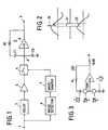
- the noise reduction circuit shown thereincomprises a series combination of a noise detector 6 and a waveshaper 7.
- the noise detectorproduces a pulse output in response to the detection of a noise impulse introduced to an audio signal applied to an input terminal 1.
- the pulse outputis shaped into a sharply defined rectangular pulse and applied as a sampling pulse to a normally closed electronic switch 4 which forms part of sample-and-hold circuit.
- the audio input signalis delayed by a delay circuit 2 so that the portion of the audio signal which is affected by the noise impulse is rendered time coincident with the sampling pulse.
- the delayed audio signalis passed through an amplifier 3 and switch 4 to a dual function amplifier circuit 5.
- This amplifier circuitcomprises a noninverting amplifier 8 and a feedback differentiator formed by a resistor R1 and a capacitor C1 which are series connected from the output of amplifier 8 to the input thereof to which the output of amplifier 3 is also applied through switch 4.
- Amplifier 3 and switch 4form a sample-and-hold circuit with a second capacitor C2 which is grounded at one end and connected at the other end to the first capacitor C1 forming a node A therebetween.
- Dual function amplifier circuit 5operates as a linear amplifier when switch 4 remains closed and as a slope detector when this switch is open to generate a linearly varying voltage for interpolating the noise-affected portion of the input signal.
- This noninverting ampliferhas an input impedance much higher than the output impedance of amplifier 3.
- switch 4In the absence of a noise impulse, switch 4 remains in a closed circuit condition, coupling the input signal to the node A. Since the output impedance of amplifier 3 is much lower than the input impedance of amplifier 8, the feedback differentiator ceases to function or disabled during the closed circuit condition with the result that capacitor C2 is charged to the voltage of the input signal. The voltage on capacitor C2 is amplified and delivered to an output terminal 9. Therefore, the potential atterminal 9 follows the voltage on capacitor C2 as long as the audio signal is not affected by noise impulses.
- a sampling pulse 21is generated and switch 4 changes over to an open circuit condition.
- the voltagewhich appeared at the moment immediately prior to the detection of the noise, is sampled and stored in capacitor C2 and amplified with gain G to appear at the output terminal 9.
- the feedback circuitis now enabled to begin differentiating the output of amplifier 8.
- the differentiated voltageis divided at the node A by capacitors C1 and C2.
- voltage on capacitor C2varies linearly with a positive or negative gradient, slope ratio, depending on the voltage sampled at the instant just prior to the detection of the noise provided that the capacitance ratio C2/C1 substantially equals the gain G of noninverting amplifer 8.
- the noise-affected portion of the audio signalis interpolated with a linearly varying voltage as shown at 22 in Fig. 2. If impulse noise occurs on a positive or uphill slope of the information signal, the interpolating voltage increases linearly, and if it occurs on a negative or downhill slope the voltage will decrease linearly.
- Equation 1A mathematical analysis of the noise reduction circuit of Fig. 1 is given with reference to an equivalent circuit shown in Fig. 3.
- the voltage output Vo(s) which appears at terminal 9 at the instant the open circuit condition occursis given in Laplace transform notation by Equation 1: where R 1 is the value of resistor R1 and e 10 and e 20 represent voltages developed respectively on capacitors C1 and C2 immediately prior to the detection of a noise impulse and I (s) is the current passing through resistor R 1 which is given as follows:
- Equation 8represents a Tailor's series excluding the differential terms of second or higher orders. It is seen from Equation 8 that the compensating voltage varies linearly at a rate V'(t 1 ) which is the first order differentiation of the voltage t time t 1 and with which previous gradient is expected to continue.
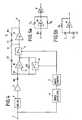
- a second embodiment of the present invention illustrated in Fig. 4is advantageous for audio signals whose higher frequency components are preemphasized.
- the second embodimentdiffers from the previous embodiment in that it additionally includes a deemphasis circuit.
- This deemphasis circuitcomprises an inverting amplifier 10 having a grounded noninverting input terminal and an inverting input terminal which is coupled by a resistor R2 to the output of amplifier 3, and a parallel combination of a resistor R3 and a normally open switch 11 connected across the inverting input and output terminals of amplifier 10.
- Amplifier 10has a low impedance at the output terminal thereof which is connected through normally closed switch 4 to amplifier 8.
- the terminal of capactor C2which is connected to ground in the previous embodiment is connected to a node B between resistor R2 and the inverting input of amplifier 10.
- Switch 11is responsive to the sampling pulse to provide a short-circuit path from node B to ground.
- the circuit of Fig. 4can be represented by an equivalent circuit shown in Fig 5a in the absence of impulse noise and the transfer function G)s) of this equivalent circuit is given by: where T is a time constant C 2 x R 3 . This time constant value is selected so that the noise reduction circuit exhibits a deemphasis characteristic on the higher frequency components of a preemphasized audio signal applied to input terminal 1.
Landscapes
- Amplifiers (AREA)
Description
- The present invention is related to the following copending United States Patent Applications:
- 1) Serial number 516,242, filed July 21, 1983, by Ishigaki et al, titled "circuit for Reconstructing Noise-Affected Signals";
- 2) Serial number 517,985, filed July 29, 1983, by Y. Ishigaki, titled "Circuit Arrangement for Reconstructing Noise-Affected Signals";
- 3) Serial number 585,925, filed March 2, 1983, by Y. Ishigaki et al, titled "Impulse noise reduction by linear interpolation having a deemphasis characteristic"; and
- 4) Serial number 585,926, filed March 2, 1983, by Y. Ishigaki et al, titled "Noise reduction by linear interpolation having immunity to white noise".
- All of the copending applications are assigned to the same assignee as the present invention.
- The present invention relates to a noise reduction circuit of the type wherein the noise-affected portion of an information signal is linearly interpolated.
- Linear interpolation techniques are known in the art (US-A-4311963) as a means of reconstructing the portion of audio signals which is disrupted by a noise impulse. As shown and described in the above listed copending U.S. applications, the linear interpolation approach involves the use of two sample-and-hold circuits. The first sample-and-hold circuit is connected in a circuit between input and output terminals for generating a voltage which follows the waveform of the input signal during tracking modes and samples a voltage that occurs immediately prior to the detection of a noise impulse. During a sampling mode in which the information signal is affected by a noise impulse, the second sample-and-hold circuit generates a voltage that represents the rate at which previous gradient is expected to continue during this period and compensates for the voltage stored on the first sample-and-hold circuit.
- An object of the present invention is to simplify the configuration of a noise reduction circuit by eliminating the second sample sample-and-hold circuit.
- The noise reduction circuit of the present invention comprises a noise detector connected to an input terminal for detecting a noise impulse introduced in an information signal and generating a sampling pulse time-coincident with the portion of the signal affected by a noise impulse. A switch is provided for passing the information signal therethrough a node between a capacitor and a noninverting amplifier in the absence of the sampling signal and blocking the signal in response to the sampling pulse. A differentiator is connected in a feedback circuit from the output of the noninverting amplifier to the node. The capacitor stores a voltage from the switch during the absence of noise and a voltage from the differentiator when the switch opens in response to the noise The differentiator is disabled when the switch remains closed and, when it opens begins differentiating a voltage which occurred immediately prior to the detection of the noise and supplies it to the capactor to linearly interpolate the portion of the information signal which is disrupted by the noise.
- The present invention will be described in further details with reference to the accompanying drawings, in which:
- Fig. 1 is a block diagram of a first embodiment of the present invention;
- Fig. 2 is an illustration of waveforms generated in the circuit of Fig. 1;
- Fig. 3 is an illustration of an equivalent circuit;
- Fig. 4 is a block diagram of a second embodiment of the present invention; and
- Figs. 5a and 5b are illustrations of equivalant circuits of the Fig. 4 circuit.
- Referring now to Fig. 1 there is shown a first embodiment of the present invention. The noise reduction circuit shown therein comprises a series combination of a
noise detector 6 and awaveshaper 7. The noise detector produces a pulse output in response to the detection of a noise impulse introduced to an audio signal applied to an input terminal 1. The pulse output is shaped into a sharply defined rectangular pulse and applied as a sampling pulse to a normally closedelectronic switch 4 which forms part of sample-and-hold circuit. The audio input signal is delayed by adelay circuit 2 so that the portion of the audio signal which is affected by the noise impulse is rendered time coincident with the sampling pulse. - The delayed audio signal is passed through an
amplifier 3 and switch 4 to a dual function amplifier circuit 5. This amplifier circuit comprises anoninverting amplifier 8 and a feedback differentiator formed by a resistor R1 and a capacitor C1 which are series connected from the output ofamplifier 8 to the input thereof to which the output ofamplifier 3 is also applied throughswitch 4. Amplifier 3 and switch 4 form a sample-and-hold circuit with a second capacitor C2 which is grounded at one end and connected at the other end to the first capacitor C1 forming a node A therebetween.- Dual function amplifier circuit 5 operates as a linear amplifier when
switch 4 remains closed and as a slope detector when this switch is open to generate a linearly varying voltage for interpolating the noise-affected portion of the input signal. This noninverting amplifer has an input impedance much higher than the output impedance ofamplifier 3. - In the absence of a noise impulse,
switch 4 remains in a closed circuit condition, coupling the input signal to the node A. Since the output impedance ofamplifier 3 is much lower than the input impedance ofamplifier 8, the feedback differentiator ceases to function or disabled during the closed circuit condition with the result that capacitor C2 is charged to the voltage of the input signal. The voltage on capacitor C2 is amplified and delivered to anoutput terminal 9. Therefore, the potential atterminal 9 follows the voltage on capacitor C2 as long as the audio signal is not affected by noise impulses. - In response to the detection of a noise impulse, shown at 20 in Fig. 2, a
sampling pulse 21 is generated and switch 4 changes over to an open circuit condition. The voltage, which appeared at the moment immediately prior to the detection of the noise, is sampled and stored in capacitor C2 and amplified with gain G to appear at theoutput terminal 9. The feedback circuit is now enabled to begin differentiating the output ofamplifier 8. The differentiated voltage is divided at the node A by capacitors C1 and C2. As will be understood by a mathematical analysis given below, voltage on capacitor C2 varies linearly with a positive or negative gradient, slope ratio, depending on the voltage sampled at the instant just prior to the detection of the noise provided that the capacitance ratio C2/C1 substantially equals the gain G ofnoninverting amplifer 8. The noise-affected portion of the audio signal is interpolated with a linearly varying voltage as shown at 22 in Fig. 2. If impulse noise occurs on a positive or uphill slope of the information signal, the interpolating voltage increases linearly, and if it occurs on a negative or downhill slope the voltage will decrease linearly. - A mathematical analysis of the noise reduction circuit of Fig. 1 is given with reference to an equivalent circuit shown in Fig. 3. The voltage output Vo(s) which appears at
terminal 9 at the instant the open circuit condition occurs is given in Laplace transform notation by Equation 1:

- The voltage input Vi(s) to terminal 1 is given by:


Equation 7 results in the following Equation:
Equation 8 represents a Tailor's series excluding the differential terms of second or higher orders. It is seen fromEquation 8 that the compensating voltage varies linearly at a rate V'(t1) which is the first order differentiation of the voltage t time t1 and with which previous gradient is expected to continue.- A second embodiment of the present invention illustrated in Fig. 4 is advantageous for audio signals whose higher frequency components are preemphasized. The second embodiment differs from the previous embodiment in that it additionally includes a deemphasis circuit. This deemphasis circuit comprises an inverting
amplifier 10 having a grounded noninverting input terminal and an inverting input terminal which is coupled by a resistor R2 to the output ofamplifier 3, and a parallel combination of a resistor R3 and a normallyopen switch 11 connected across the inverting input and output terminals ofamplifier 10.Amplifier 10 has a low impedance at the output terminal thereof which is connected through normally closedswitch 4 toamplifier 8. In this embodiment, the terminal of capactor C2 which is connected to ground in the previous embodiment is connected to a node B between resistor R2 and the inverting input ofamplifier 10.Switch 11 is responsive to the sampling pulse to provide a short-circuit path from node B to ground. - During the closed circuit condition of
switch 4,switch 11 is open and node A is at near ground potential due to the low output impedance ofamplifier 10. The feedback circuit of R1 and C1 is therefore disabled as in the first embodiment. The circuit of Fig. 4 can be represented by an equivalent circuit shown in Fig 5a in the absence of impulse noise and the transfer function G)s) of this equivalent circuit is given by:
- In the presence of a noise impulse,
switch 4 is open and switch 11 is closed. The node B is thus shortcircuited to ground throughswitch 11 and the output terminal ofamplifier 10 to the grounded noninverting input terminal thereof, disabling the deemphasis circuit. The noise reduction circuit is switched to a condition which is represented by an equivalent circuit shown in Fig. 5b which is identical to the previous embodiment.


Claims (6)
Applications Claiming Priority (4)
| Application Number | Priority Date | Filing Date | Title |
|---|---|---|---|
| JP14024183AJPS6031319A (en) | 1983-07-30 | 1983-07-30 | Device for reducing pulse noise |
| JP140241/83 | 1983-07-30 | ||
| JP15004583AJPS6041823A (en) | 1983-08-17 | 1983-08-17 | Reduction device of impulsive noise |
| JP150045/83 | 1983-08-17 |
Publications (3)
| Publication Number | Publication Date |
|---|---|
| EP0135081A2 EP0135081A2 (en) | 1985-03-27 |
| EP0135081A3 EP0135081A3 (en) | 1988-01-07 |
| EP0135081B1true EP0135081B1 (en) | 1990-01-31 |
Family
ID=26472829
Family Applications (1)
| Application Number | Title | Priority Date | Filing Date |
|---|---|---|---|
| EP84109015AExpiredEP0135081B1 (en) | 1983-07-30 | 1984-07-30 | Noise reduction by linear interpolation using a dual function amplifier circuit |
Country Status (3)
| Country | Link |
|---|---|
| US (1) | US4539527A (en) |
| EP (1) | EP0135081B1 (en) |
| DE (1) | DE3481245D1 (en) |
Families Citing this family (17)
| Publication number | Priority date | Publication date | Assignee | Title |
|---|---|---|---|---|
| DE4122520A1 (en)* | 1991-07-08 | 1993-01-14 | Blaupunkt Werke Gmbh | CONTROL DEVICE FOR AN FM RECEIVER WITH MULTIPLE ANTENNAS |
| DE69221434T2 (en)* | 1991-11-15 | 1997-12-11 | Asahi Glass Co Ltd | Image display device and method for controlling the same |
| KR0182943B1 (en)* | 1995-02-04 | 1999-04-15 | 김광호 | Noise filtering circuit for audio signal |
| US6473253B1 (en)* | 1999-04-28 | 2002-10-29 | Koninklijke Philips Electronics N.V. | Read channel with programmable bandwidth control |
| US6781426B2 (en)* | 2001-07-26 | 2004-08-24 | The Regents Of The University Of California | Nanosecond monolithic CMOS readout cell |
| WO2006098323A1 (en)* | 2005-03-17 | 2006-09-21 | Pioneer Corporation | Noise canceller |
| EP2491478A4 (en)* | 2009-10-20 | 2014-07-23 | Cypress Semiconductor Corp | Method and apparatus for reducing coupled noise influence in touch screen controllers. |
| US8583033B2 (en)* | 2010-03-05 | 2013-11-12 | Wilson Electronics, Llc | Oscillation protected amplifier with base station overload and noise floor protection |
| CN102844669B (en)* | 2010-08-24 | 2016-06-15 | 赛普拉斯半导体公司 | Noise suppression circuit and method for capacitive sensing system |
| US9323385B2 (en)* | 2011-04-05 | 2016-04-26 | Parade Technologies, Ltd. | Noise detection for a capacitance sensing panel |
| US8639180B2 (en) | 2011-08-23 | 2014-01-28 | Wilson Electronics, Llc | Verifying and mitigating oscillation in amplifiers |
| US8849187B2 (en) | 2011-08-23 | 2014-09-30 | Wilson Electronics, Llc | Radio frequency amplifier noise reduction system |
| US8874029B2 (en) | 2011-08-23 | 2014-10-28 | Wilson Electronics, Llc | Verifying oscillation in amplifiers and the mitigation thereof |
| US8583034B2 (en) | 2011-08-23 | 2013-11-12 | Wilson Electronics, Llc | Verifying and mitigating oscillation in amplifiers |
| US8874030B2 (en) | 2011-08-23 | 2014-10-28 | Wilson Electronics, Llc | Oscillation detection and oscillation mitigation in amplifiers |
| CA2814303A1 (en) | 2013-04-26 | 2014-10-26 | Cellphone-Mate, Inc. | Apparatus and methods for radio frequency signal boosters |
| US10673518B2 (en) | 2017-06-27 | 2020-06-02 | Wilson Electronics, Llc | Crossover isolation reduction in a signal booster |
Family Cites Families (1)
| Publication number | Priority date | Publication date | Assignee | Title |
|---|---|---|---|---|
| US4311963A (en)* | 1978-07-18 | 1982-01-19 | Matsushita Electric Industrial Co., Ltd. | Noise pulse suppressing system |
- 1984
- 1984-07-27USUS06/635,352patent/US4539527A/ennot_activeExpired - Lifetime
- 1984-07-30DEDE8484109015Tpatent/DE3481245D1/ennot_activeExpired - Fee Related
- 1984-07-30EPEP84109015Apatent/EP0135081B1/ennot_activeExpired
Also Published As
| Publication number | Publication date |
|---|---|
| US4539527A (en) | 1985-09-03 |
| EP0135081A2 (en) | 1985-03-27 |
| EP0135081A3 (en) | 1988-01-07 |
| DE3481245D1 (en) | 1990-03-08 |
Similar Documents
| Publication | Publication Date | Title |
|---|---|---|
| EP0135081B1 (en) | Noise reduction by linear interpolation using a dual function amplifier circuit | |
| US4152659A (en) | Low noise differential amplifier | |
| KR910000368B1 (en) | Nonlinear Signal Processing Device | |
| EP0400725B1 (en) | Sample-and-hold device | |
| US4577161A (en) | Noise reduction by linear interpolation using a dual function amplifier circuit | |
| US4555669A (en) | Noise reduction by linear interpolation using a single sample-and-hold circuit | |
| US4847523A (en) | Lock-in test amplifier | |
| US4140928A (en) | Monostable multivibrator | |
| US4468627A (en) | RIAA Equalizer circuit | |
| US4531095A (en) | Impulse noise reduction by linear interpolation having immunity to white noise | |
| GB2138231A (en) | Signal transmission circuit | |
| US4247823A (en) | Low noise, low phase shift analog signal multiplier | |
| US5793243A (en) | Method of stabilizing an electronic signal integrator | |
| US6028469A (en) | Electric circuit arrangement comprising a switchable feedback branch | |
| US4271535A (en) | Noise eliminating system | |
| EP0322803A2 (en) | Automatic gain control amplifier for compensating cable loss | |
| US4532475A (en) | Impulse noise reduction by linear interpolation having a deemphasis characteristic | |
| US4803701A (en) | Digital detection circuit | |
| JPS6218095B2 (en) | ||
| US4303889A (en) | Filter circuit | |
| US4517534A (en) | Circuit detector and noise reduction network with circuit detector | |
| US4404517A (en) | Impedance measuring device | |
| US2776369A (en) | Video integrator circuits | |
| US3497805A (en) | Circuit including a constant amplitude pulse generator for adjusting the amplitude of pulses produced by a transducer | |
| US3234408A (en) | Pulse producing capacitor circuits including one or more commutating switches |
Legal Events
| Date | Code | Title | Description |
|---|---|---|---|
| PUAI | Public reference made under article 153(3) epc to a published international application that has entered the european phase | Free format text:ORIGINAL CODE: 0009012 | |
| AK | Designated contracting states | Designated state(s):DE FR GB | |
| PUAL | Search report despatched | Free format text:ORIGINAL CODE: 0009013 | |
| AK | Designated contracting states | Kind code of ref document:A3 Designated state(s):DE FR GB | |
| 17P | Request for examination filed | Effective date:19880111 | |
| 17Q | First examination report despatched | Effective date:19890510 | |
| GRAA | (expected) grant | Free format text:ORIGINAL CODE: 0009210 | |
| AK | Designated contracting states | Kind code of ref document:B1 Designated state(s):DE FR GB | |
| REF | Corresponds to: | Ref document number:3481245 Country of ref document:DE Date of ref document:19900308 | |
| ET | Fr: translation filed | ||
| PLBE | No opposition filed within time limit | Free format text:ORIGINAL CODE: 0009261 | |
| STAA | Information on the status of an ep patent application or granted ep patent | Free format text:STATUS: NO OPPOSITION FILED WITHIN TIME LIMIT | |
| 26N | No opposition filed | ||
| REG | Reference to a national code | Ref country code:GB Ref legal event code:IF02 | |
| PGFP | Annual fee paid to national office [announced via postgrant information from national office to epo] | Ref country code:FR Payment date:20020709 Year of fee payment:19 | |
| PGFP | Annual fee paid to national office [announced via postgrant information from national office to epo] | Ref country code:GB Payment date:20020724 Year of fee payment:19 | |
| PGFP | Annual fee paid to national office [announced via postgrant information from national office to epo] | Ref country code:DE Payment date:20020807 Year of fee payment:19 | |
| PG25 | Lapsed in a contracting state [announced via postgrant information from national office to epo] | Ref country code:GB Free format text:LAPSE BECAUSE OF NON-PAYMENT OF DUE FEES Effective date:20030730 | |
| PG25 | Lapsed in a contracting state [announced via postgrant information from national office to epo] | Ref country code:DE Free format text:LAPSE BECAUSE OF NON-PAYMENT OF DUE FEES Effective date:20040203 | |
| GBPC | Gb: european patent ceased through non-payment of renewal fee | Effective date:20030730 | |
| PG25 | Lapsed in a contracting state [announced via postgrant information from national office to epo] | Ref country code:FR Free format text:LAPSE BECAUSE OF NON-PAYMENT OF DUE FEES Effective date:20040331 | |
| REG | Reference to a national code | Ref country code:FR Ref legal event code:ST |