EP0134560B1 - Electrical switch - Google Patents
Electrical switchDownload PDFInfo
- Publication number
- EP0134560B1 EP0134560B1EP84109762AEP84109762AEP0134560B1EP 0134560 B1EP0134560 B1EP 0134560B1EP 84109762 AEP84109762 AEP 84109762AEP 84109762 AEP84109762 AEP 84109762AEP 0134560 B1EP0134560 B1EP 0134560B1
- Authority
- EP
- European Patent Office
- Prior art keywords
- plunger
- casing
- fixed contacts
- switch
- lead terminals
- Prior art date
- Legal status (The legal status is an assumption and is not a legal conclusion. Google has not performed a legal analysis and makes no representation as to the accuracy of the status listed.)
- Expired
Links
- 239000000758substrateSubstances0.000claimsdescription8
- 230000002093peripheral effectEffects0.000claimsdescription7
- 239000000919ceramicSubstances0.000claimsdescription4
- 229920001707polybutylene terephthalatePolymers0.000claimsdescription3
- 229910000881Cu alloyInorganic materials0.000claimsdescription2
- PNEYBMLMFCGWSK-UHFFFAOYSA-Naluminium oxideInorganic materials[O-2].[O-2].[O-2].[Al+3].[Al+3]PNEYBMLMFCGWSK-UHFFFAOYSA-N0.000claimsdescription2
- DMFGNRRURHSENX-UHFFFAOYSA-Nberyllium copperChemical compound[Be].[Cu]DMFGNRRURHSENX-UHFFFAOYSA-N0.000claimsdescription2
- -1polybutylene terephthalatePolymers0.000claimsdescription2
- 239000010935stainless steelSubstances0.000claimsdescription2
- 229910001220stainless steelInorganic materials0.000claimsdescription2
- 239000011347resinSubstances0.000claims1
- 229920005989resinPolymers0.000claims1
- 230000004048modificationEffects0.000description9
- 238000012986modificationMethods0.000description9
- 239000000463materialSubstances0.000description8
- 238000005476solderingMethods0.000description3
- 230000008602contractionEffects0.000description2
- 239000013307optical fiberSubstances0.000description2
- 238000010276constructionMethods0.000description1
- 230000006866deteriorationEffects0.000description1
- 238000010586diagramMethods0.000description1
- 238000006073displacement reactionMethods0.000description1
- 238000010292electrical insulationMethods0.000description1
- 230000001747exhibiting effectEffects0.000description1
- 238000011835investigationMethods0.000description1
- 238000004519manufacturing processMethods0.000description1
- 238000007789sealingMethods0.000description1
- 229920003002synthetic resinPolymers0.000description1
- 239000000057synthetic resinSubstances0.000description1
- 238000003466weldingMethods0.000description1
Images


Classifications
- H—ELECTRICITY
- H01—ELECTRIC ELEMENTS
- H01H—ELECTRIC SWITCHES; RELAYS; SELECTORS; EMERGENCY PROTECTIVE DEVICES
- H01H1/00—Contacts
- H01H1/58—Electric connections to or between contacts; Terminals
- H—ELECTRICITY
- H01—ELECTRIC ELEMENTS
- H01H—ELECTRIC SWITCHES; RELAYS; SELECTORS; EMERGENCY PROTECTIVE DEVICES
- H01H13/00—Switches having rectilinearly-movable operating part or parts adapted for pushing or pulling in one direction only, e.g. push-button switch
- H01H13/02—Details
- H01H13/12—Movable parts; Contacts mounted thereon
- H01H13/14—Operating parts, e.g. push-button
- H01H13/18—Operating parts, e.g. push-button adapted for actuation at a limit or other predetermined position in the path of a body, the relative movement of switch and body being primarily for a purpose other than the actuation of the switch, e.g. door switch, limit switch, floor-levelling switch of a lift
- H—ELECTRICITY
- H01—ELECTRIC ELEMENTS
- H01H—ELECTRIC SWITCHES; RELAYS; SELECTORS; EMERGENCY PROTECTIVE DEVICES
- H01H9/00—Details of switching devices, not covered by groups H01H1/00 - H01H7/00
- H01H9/02—Bases, casings, or covers
Definitions
- the present inventionrelates to an electrical switch according to the preamble of claim 1.
- a switch of this typeis known from US-A-2712047.
- This known switchis provided with movable and fixed contacts which are both sheet- like.
- the movable contactsare provided separately from the plunger and lie behind the same in the axial direction of the switch so that a gap is formed between the plunger and the movable contacts when the plunger is in the free state. This gap forms a play between the plunger and the movable contact which has to be overcome for the switch to respond to a depression of the plunger.
- the switchsince the movable contact, the fixed contacts and the restoring spring are provided at an intermediate portion of and around a plunger the switch may be constructed to be extremely compact in the longitudinal direction of the plunger, and owing to the fact that the sliding span of the plunger may be set comparatively long, while the contacts are formed into a cross bar long, construction through the employment of rod members, highly accurate functioning on the contacts may be achieved. Moreover, by forming the contacts from rod members, the overall cost for the switch may be appreciably reduced.
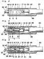
- an electrical switchwhich generally includes an inner casing 1, fixed contacts 8 and 9, lead terminals 10 and 15, a plunger 30, a movable contact 35, bearing members 36 and 37, a return spring 38, and an outer casing 45.
- the inner casing 1is molded as one unit by a proper synthetic resin or the like, and the lead .terminals 10 and 15 are integrally blanked from an electrically conductive metallic thin plate by press work, while the fixed contacts 8 and 9 are prepared by cutting a contact material in the form of a round rod into a predetermined length.
- These fixed contacts 8 and 9are each fixed to projections 11 and 16 of the lead terminals 10 and 15 by spot welding at one end face thereof, and are inserted into through-holes 3 formed in the inner casing 1 in a direction intersecting at right angles with a central bore 2 of said inner casing 1. In the inserted state, the fixed contacts 8 and 9 are exposed at their central portions within the central bore 2 to confront each other.
- the lead terminals 10 and 15have cores 21 of an external cord 20 preliminarily soldered at semi-circular curved portions 12 and 17 thereof, and are fitted into corresponding stepped portions or recesses 4 formed on the outer peripheral surface of the inner casing 1.
- the lead terminals 10 and 15themselves are temporarily fixed to the casing 1 by fitting small projections 5 provided on the recesses 4 into corresponding holes 13 and 18 formed in said lead terminals.
- the recesses 4 referred to aboveare formed in the configuration generally similar to that of the lead terminals 10 and 15 on the outer peripheral surface of the inner casing 1. As shown in Fig.
- a width W1 of the lead terminals 10 and 15 in a free stateis formed to be slightly larger than a width W2 in a circumferential direction of the recess 4, and the lead terminals 10 and 15 are fitted into the recesses 4 in the state where they are deflected to be directed along the outer peripheral surface of the inner casing 1.
- the opposite ends of the respective lead terminals 10 and 15engage the side wall portions 4a of the recesses 4 by a spring force or resiliency of their own so as to be prevented from falling off.
- the side wall portions 4a of the recesses 4are required to have a shape or angle suitable for receiving the spring force of the lead terminals 10 and 15, and in the present embodiment, each of said wall portions 4a has a plane parallel to the direction for attaching the lead terminal 10 or 15. Meanwhile, the lead terminals 10 and 15 are prevented from falling off also by fitting the holes 13 and 18 thereof over the small projections 5.
- the fixing by the side wall portions 4a and the small projections 5is termporary only during assembling, lead terminals 10 and 15 are subjected to a positive fixing as well as an electrical insulation by applying a heat shrinkable tube 22 thereover later.
- heat caulking or staking of the small projections 5may be considered, but this is not necessarily preferable since it would mean an increase of manufacturing steps.
- the plunger 30is slidably provided in the central bore 2 of the inner casing 1 through bearing members 36 and 37 made, for example, of ceramics, with the movable contact 35 being inserted into a hole 31 formed at approximately an intermediate portion of said plunger 30.
- This movable contact 35is prepared by cutting a contact material in the form of a round rod to a predetermined length, i.e. to a length slightly longer than a span of the fixed contacts 8 and 9, and is positioned in a direction to intersect with the fixed contacts 8 and 9.
- groove portions 6are formed so as to allow the opposite end portions of the movable contact 35 to be displaced.
- the return spring 38in a coil-like shape is disposed in a compressed state through a washer 39 (Fig. 4) so as to normally urge the movable contact 35 and the plunger 30 in the direction of the arrow a for providing a contact pressure by which the movable contact 35 is held in pressure contact with the fixed contacts 8 and 9.
- the bearing member 37, return spring 38 and the plunger 30 having the movable contact 35are inserted into the central bore 2 of the inner casing 1, and the fixed contacts 8 and 9 are inserted into the through-openings 3, in the state where the plunger 30 has been pressed into the central bore 2.
- the outer casing 45is made of a metallic cylinder with a thread 46 partly eliminated by a flat plane being formed on the outer peripheral surface thereof.
- the inner casing 1is inserted into the outer casing 45 from its rear end opening and accommodated with the forward end portion of the plunger 30 projecting out of an opening 47 of outer casing 45.
- a bellow-like expansion and contraction rubber member 44is fitted for sealing of the opening 47.
- the movable contact 35normally contacts the fixed contacts 8 and 9 by the spring force of the return spring 38 to keep the switch in the closed state.
- the movable contact 35Upon depression of the plunger 30 in the direction of the arrow a', the movable contact 35 is displaced together with the plunger 30 against the spring force of the return spring 38 in the direction of the arrow a', and thus, the fixed contacts 8 and 9 are spaced from the movable contact 35 for opening.
- the electrical switch as described abovemay be mounted on a panel (not shown) or the like, by inserting the outer casing 45 into a mounting hole (not shown) of the panel, etc. and engaging nuts (not shown) onto the female thread 46 thereof from the front side and rear side of the panel.
- the fixed contacts 8 and 9are immediately opened upon depression of the plunger 30, the movement up to the functioning (PT) being practically zero.
- the functioning accuracy of the contactshas been remarkably improved.
- the plunger 30is supported at the opposite ends by the bearing members 36 and 37, with a comparatively long sliding span L being available, influences due to a side play resulting from dimensional errors, etc. may be eliminated as far as practicable.
- the movable contact 35is provided at approximately the intermediate portion of the plunger 30, while the return spring 38 and the fixed contacts 8 and 9 are disposed around the plunger 30, the space is efficiently utilized to constitute a switch of a compact size. Furthermore, by forming the contacts 8, 9 and 35 from a rod material, especially a round rod, the switch may be produced at low cost.
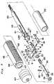
- an electrical switchaccording to a second embodiment of the present invention.
- the arrangement of the inner casing 1, fixed contacts 8 and 9, lead terminals 10 and 15, plunger 30, movable contact 35, and outer casing 45, etc.is generally similar to that of the first embodiment.
- a switching circuitin the form of an IC circuit between the lead terminals 10 and 15 and the external cord 20.
- the above switching circuitincludes two transistors Tr1 and Tr2 forming the known non-contact switch, with a Zener diode ZD for protection and a light emitting diode LED being inserted therebetween.
- the switching circuit as described aboveis formed on a printed substrate 40, with the light emitting diode LED being connected to one end portion of an optical fiber 41 through a transparent heat-shrinkable tube 42.
- a window portion 49(Fig. 6) in a position corresponding to the disposed position of the light emitting diode LED. Accordingly, the light of the light emitting diode LED may be observed at the forward end portion of the optical fiber 41 and the window portion 49 of the outer casing 45.
- the non-contact signals from the transistors Tr1 and Tr2may be derived, and in spite of the fact that the current flowing through the fixed contacts 8 and 9 is of a small quantity, a large amount of current may be caused to flow through the terminals T1 and T2.
- a small amount of currentflows through the contacts 8, 9 and 35 even if a large amount of current is to be opened or closed, deterioration of the contacts may be reduced, so that the switch withstands a repeated use for a long period, with open/close characteristics at high accuracy being maintained.
- connection between each core 21 and the substrate 40may be modified as shown in Figs. 8(a), 8(b) and 8(c).
- pins 61 of a connector 60 attached to one end of the external cord 20are soldered to terminals 51 soldered to fixing holes 40a of the printed substrate 40.
- the terminals 51are formed by press work as a terminal plate 50 so as to be preliminarily connected in one unit at a connecting portion 52, and the connecting portion 52 is adapted to be folded off at groove portions 53 formed into a triangular cross section.
- this terminal plate 50is inserted, at the terminals 51 thereof, into the fixing holes 40a of the printed substrate 40 for soldering, while the pins 61 of the connector 60 are soldered for connection of the wiring on the substrate 40 with the external cord 20, and thereafter, the connecting portion 52 is folded in the direction of an arrow F to break off said portion 52 (Fig. 8(c)) at the groove portions 53.
- the terminals 51are formed into one unit by the connecting portion 52, they may be handled as a comparatively large part, and although the terminals 51 themselves are of symmetrically different shapes, they are not wrongly selected in assembling and can be readily inserted into the fixing holes 40a by one operation. If the terminals 51 were disposed separately, they would move relative to each other during the soldering of the pins 61 of the connector 60. But being provided as one unit as described above, the soldering of the pins 61 is facilitated without an undesirable movement thereof during assembling.
- Fig. 9is shown a further modification of the electrical switch according to the present invention.
- this modificationit is intended to provide a high precision electrical switch in which scattering or deviation of the operating positions is extremely small with respect to temperature variations.
- a high precision contact functioningmay be realized, since the movable contact is immediately spaced from the fixed contacts upon depression of the plunger and thus, the movement up to the functioning (PT) is zero, but it is not necessarily considered so far that the functioning position of the contacts is constant even with respect to the temperature variations.
- the inner casing 1is molded as one unit from PBT (polybutylene terephthalate).
- the lead terminals 10 and 15are integrally blanked from an electrically conductive thin plate by press work, while the fixed contacts 8 and 9 are prepared by cutting a contact material in the form of a round rod made of a beryllium-copper alloy to a predetermined length.
- the plunger 30is composed of ceramics of alumina, and the bearing members 36 and 37 provided in the central bore 2 of the inner casing 1 are made of ceramics.
- the movable contact 35is prepared by a contact material in the form of a round rod, cut into a predetermined length slightly longer than the span of the fixed contacts 8 and 9.
- the outer casing 45is formed into a generally cylindrical shape from a stainless steel material, and has a pair of projections 70 provided at opposite sides in the forward portion thereof, with fixing holes 71 for fixing the switch to a panel or the like by screws being formed in said projections 70.
- Expansion or contraction of the respective members resulting from the temperature variationsexerts influence on a distance L from the center of the fixing hole 71 as the reference position to the forward end of the plunger 30.
- the expansion of the outer casing 45 and the plunger 30acts in the direction of the arrow a
- the expansion of the inner casing 1 and the fixed contacts 8 and 9acts in the direction of the arrow a'.
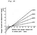
- Fig. 10there is shown a graph showing variation characteristics of functioning points with respect to temperatures in the electrical switch of Fig. 9.
- the abscissarepresents the distance L3 from the forward end of the plunger to the contact point in mm, while the ordinate denotes the variation amount at the forward end of the plunger.
Landscapes
- Physics & Mathematics (AREA)
- Electromagnetism (AREA)
- Push-Button Switches (AREA)
Description
- The present invention relates to an electrical switch according to the preamble of
claim 1. - A switch of this type is known from US-A-2712047. This known switch is provided with movable and fixed contacts which are both sheet- like. The movable contacts are provided separately from the plunger and lie behind the same in the axial direction of the switch so that a gap is formed between the plunger and the movable contacts when the plunger is in the free state. This gap forms a play between the plunger and the movable contact which has to be overcome for the switch to respond to a depression of the plunger.
- It is an object of the invention to provide a switch of the kind defined in the outset which is reliable in operation exhibiting a quick switching response to a displacement of the plunger and which, at the same time, is compact in the axial direction of the switch.
- This object is achieved by a switch as claimed in
claim 1. - According to such an arrangement, since the movable contact, the fixed contacts and the restoring spring are provided at an intermediate portion of and around a plunger the switch may be constructed to be extremely compact in the longitudinal direction of the plunger, and owing to the fact that the sliding span of the plunger may be set comparatively long, while the contacts are formed into a cross bar long, construction through the employment of rod members, highly accurate functioning on the contacts may be achieved. Moreover, by forming the contacts from rod members, the overall cost for the switch may be appreciably reduced.
- Preferred embodiments of the invention are now described with reference to the accompanying drawings, in which;
- Fig. 1 is an exploded perspective view of an electrical switch according to one preferred embodiment of the present invention,
- Fig. 1 (a) is a cross sectional view showing a state where lead terminals are fitted into corresponding recesses of a casing employed in the electrical switch of Fig. 1,
- Fig. 2 is a front elevational view of the electrical switch of Fig. 1 in which an outer casing is sectioned,
- Fig. 3 is a vertical cross section at a central portion of the electrical switch of Fig. 1,
- Fig. 4 is a horizontal cross section at a central portion of the electrical switch of Fig. 1,
- Fig. 5 is an exploded perspective view similar to Fig. 1, which particularly shows a second embodiment thereof,
- Fig. 6 is a vertical cross section at a central portion of the electrical switch of Fig. 1,
- Fig. 7 is an electrical circuit diagram showing a switching circuit of the electrical switch of Fig. 5,
- Figs. 8(a), 8(b) and 8(c) are fragmentary perspective views showing a modification related to the connection between fixed contacts and an external cord,
- Fig. 9 is a cross section similar to Fig. 3, which particularly shows a modification thereof wherein accuracy of functioning positions with respect to temperature variations has been improved, and
- Fig. 10 is a graph showing varying characteristics with respect to the modification of Fig. 9.
- Like parts are designated by like reference numerals throughout the accompanying drawings.
- In Figs. 1 to 4 is shown an electrical switch which generally includes an
inner casing 1, fixedcontacts lead terminals plunger 30, amovable contact 35, bearingmembers return spring 38, and anouter casing 45. - The
inner casing 1 is molded as one unit by a proper synthetic resin or the like, and the lead .terminals fixed contacts fixed contacts projections 11 and 16 of thelead terminals holes 3 formed in theinner casing 1 in a direction intersecting at right angles with acentral bore 2 of saidinner casing 1. In the inserted state, thefixed contacts central bore 2 to confront each other. Thelead terminals cores 21 of anexternal cord 20 preliminarily soldered at semi-circularcurved portions recesses 4 formed on the outer peripheral surface of theinner casing 1. Thelead terminals casing 1 by fittingsmall projections 5 provided on therecesses 4 intocorresponding holes recesses 4 referred to above are formed in the configuration generally similar to that of thelead terminals inner casing 1. As shown in Fig. 1 (a), a width W1 of thelead terminals recess 4, and thelead terminals recesses 4 in the state where they are deflected to be directed along the outer peripheral surface of theinner casing 1. In this case, the opposite ends of therespective lead terminals side wall portions 4a of therecesses 4 by a spring force or resiliency of their own so as to be prevented from falling off. Theside wall portions 4a of therecesses 4 are required to have a shape or angle suitable for receiving the spring force of thelead terminals wall portions 4a has a plane parallel to the direction for attaching thelead terminal lead terminals holes small projections 5. The fixing by theside wall portions 4a and thesmall projections 5 is termporary only during assembling,lead terminals heat shrinkable tube 22 thereover later. - Also heat caulking or staking of the
small projections 5 may be considered, but this is not necessarily preferable since it would mean an increase of manufacturing steps. - The
plunger 30 is slidably provided in thecentral bore 2 of theinner casing 1 through bearingmembers movable contact 35 being inserted into ahole 31 formed at approximately an intermediate portion of saidplunger 30. Thismovable contact 35 is prepared by cutting a contact material in the form of a round rod to a predetermined length, i.e. to a length slightly longer than a span of thefixed contacts fixed contacts - Within the
central bore 2groove portions 6 are formed so as to allow the opposite end portions of themovable contact 35 to be displaced. Around theplunger 30 and between thebearing 37 and themovable contact 35, thereturn spring 38 in a coil-like shape is disposed in a compressed state through a washer 39 (Fig. 4) so as to normally urge themovable contact 35 and theplunger 30 in the direction of the arrow a for providing a contact pressure by which themovable contact 35 is held in pressure contact with thefixed contacts - For assembling the arrangement as described so far, the
bearing member 37, returnspring 38 and theplunger 30 having themovable contact 35 are inserted into thecentral bore 2 of theinner casing 1, and thefixed contacts openings 3, in the state where theplunger 30 has been pressed into thecentral bore 2. - The
outer casing 45 is made of a metallic cylinder with athread 46 partly eliminated by a flat plane being formed on the outer peripheral surface thereof. Theinner casing 1 is inserted into theouter casing 45 from its rear end opening and accommodated with the forward end portion of theplunger 30 projecting out of an opening 47 ofouter casing 45. Into anannular groove 48 of theouter casing 45 and anotherannular groove 32 formed at the forward end of theplunger 30, a bellow-like expansion andcontraction rubber member 44 is fitted for sealing of theopening 47. - In the above arrangement, the
movable contact 35 normally contacts thefixed contacts return spring 38 to keep the switch in the closed state. Upon depression of theplunger 30 in the direction of the arrow a', themovable contact 35 is displaced together with theplunger 30 against the spring force of thereturn spring 38 in the direction of the arrow a', and thus, thefixed contacts movable contact 35 for opening. - The electrical switch as described above may be mounted on a panel (not shown) or the like, by inserting the
outer casing 45 into a mounting hole (not shown) of the panel, etc. and engaging nuts (not shown) onto thefemale thread 46 thereof from the front side and rear side of the panel. - The
fixed contacts plunger 30, the movement up to the functioning (PT) being practically zero. By forming the cross bar contacts by the round bar as contact material, the functioning accuracy of the contacts has been remarkably improved. Moreover, since theplunger 30 is supported at the opposite ends by the bearingmembers - Since the
movable contact 35 is provided at approximately the intermediate portion of theplunger 30, while thereturn spring 38 and thefixed contacts plunger 30, the space is efficiently utilized to constitute a switch of a compact size. Furthermore, by forming thecontacts - Referring to Figs. 5 through 7, there is shown an electrical switch according to a second embodiment of the present invention. In this embodiment adapted to take out a two line type non-contact output the arrangement of the
inner casing 1,fixed contacts lead terminals plunger 30,movable contact 35, andouter casing 45, etc. is generally similar to that of the first embodiment. There is further provided a switching circuit in the form of an IC circuit between thelead terminals external cord 20. As shown in Fig. 7, the above switching circuit includes two transistors Tr1 and Tr2 forming the known non-contact switch, with a Zener diode ZD for protection and a light emitting diode LED being inserted therebetween. - When a power source and a load are connected across terminals T1 and T2 of the switching circuit of Fig. 7, the transistors Tr1 and Tr2 are turned off in the case where the
fixed contacts fixed contacts - The switching circuit as described above is formed on a printed
substrate 40, with the light emitting diode LED being connected to one end portion of anoptical fiber 41 through a transparent heat-shrinkable tube 42. On the upper surface of theouter casing 45, there is formed a window portion 49 (Fig. 6) in a position corresponding to the disposed position of the light emitting diode LED. Accordingly, the light of the light emitting diode LED may be observed at the forward end portion of theoptical fiber 41 and thewindow portion 49 of theouter casing 45. According to the second embodiment as described so far, based on the on/off of the contact signals of thefixed contacts fixed contacts contacts - In the above second embodiment, the connection between each
core 21 and thesubstrate 40 may be modified as shown in Figs. 8(a), 8(b) and 8(c). - More specifically, in the modification of Figs. 8(a), 8(b) and 8(c),
pins 61 of aconnector 60 attached to one end of theexternal cord 20 are soldered toterminals 51 soldered to fixingholes 40a of the printedsubstrate 40. As shown in Figs. 8(a) and 8(b), theterminals 51 are formed by press work as aterminal plate 50 so as to be preliminarily connected in one unit at a connectingportion 52, and the connectingportion 52 is adapted to be folded off atgroove portions 53 formed into a triangular cross section. In the first place, thisterminal plate 50 is inserted, at theterminals 51 thereof, into the fixingholes 40a of the printedsubstrate 40 for soldering, while thepins 61 of theconnector 60 are soldered for connection of the wiring on thesubstrate 40 with theexternal cord 20, and thereafter, the connectingportion 52 is folded in the direction of an arrow F to break off said portion 52 (Fig. 8(c)) at thegroove portions 53. - In the above modification, since the
terminals 51 are formed into one unit by the connectingportion 52, they may be handled as a comparatively large part, and although theterminals 51 themselves are of symmetrically different shapes, they are not wrongly selected in assembling and can be readily inserted into the fixingholes 40a by one operation. If theterminals 51 were disposed separately, they would move relative to each other during the soldering of thepins 61 of theconnector 60. But being provided as one unit as described above, the soldering of thepins 61 is facilitated without an undesirable movement thereof during assembling. - In Fig. 9 is shown a further modification of the electrical switch according to the present invention. By this modification, it is intended to provide a high precision electrical switch in which scattering or deviation of the operating positions is extremely small with respect to temperature variations. In the electrical switches described so far, a high precision contact functioning may be realized, since the movable contact is immediately spaced from the fixed contacts upon depression of the plunger and thus, the movement up to the functioning (PT) is zero, but it is not necessarily considered so far that the functioning position of the contacts is constant even with respect to the temperature variations. In the modification of Fig. 9, the
inner casing 1 is molded as one unit from PBT (polybutylene terephthalate). Thelead terminals contacts plunger 30 is composed of ceramics of alumina, and the bearingmembers central bore 2 of theinner casing 1 are made of ceramics. Themovable contact 35 is prepared by a contact material in the form of a round rod, cut into a predetermined length slightly longer than the span of the fixedcontacts outer casing 45 is formed into a generally cylindrical shape from a stainless steel material, and has a pair ofprojections 70 provided at opposite sides in the forward portion thereof, with fixingholes 71 for fixing the switch to a panel or the like by screws being formed in saidprojections 70. - Here, investigations will be made on the scattering or deviation of the functioning positions with respect to temperature variations in the electrical switch of Fig 9.
- Expansion or contraction of the respective members resulting from the temperature variations, exerts influence on a distance L from the center of the fixing
hole 71 as the reference position to the forward end of theplunger 30. For example, the expansion of theouter casing 45 and theplunger 30 acts in the direction of the arrow a, and the expansion of theinner casing 1 and the fixedcontacts hole 47 to the forward end of the inner casing 1) multiplied by its temperature coefficient A with respect to theouter casing 45, a distance L3 (from the forward end of theplunger 30 to the contact point thereof) multiplied by its temperature coefficient B with respect to theplunger 30, a distance L2 (from the forward end of theinner casing 1 to the fixedcontacts 8 and 9) multiplied by the temperature coefficient C of theinner casing 1, and the diameter d of the fixedcontacts - Accordingly, in the modification of Fig. 9, in order to obtain an amount of
variation 5=0 at the functioning position, the materials and dimensions of the respective members are selected to satisfy the equation,
- In Fig. 10, there is shown a graph showing variation characteristics of functioning points with respect to temperatures in the electrical switch of Fig. 9. In this graph, the abscissa represents the distance L3 from the forward end of the plunger to the contact point in mm, while the ordinate denotes the variation amount at the forward end of the plunger.

Claims (6)

Priority Applications (1)
| Application Number | Priority Date | Filing Date | Title |
|---|---|---|---|
| AT84109762TATE49320T1 (en) | 1983-08-16 | 1984-08-16 | ELECTRICAL SWITCH. |
Applications Claiming Priority (8)
| Application Number | Priority Date | Filing Date | Title |
|---|---|---|---|
| JP127136/83U | 1983-08-16 | ||
| JP1983127136UJPS6035431U (en) | 1983-08-16 | 1983-08-16 | switch |
| JP130721/83U | 1983-08-23 | ||
| JP13072183UJPS6038436U (en) | 1983-08-23 | 1983-08-23 | switch |
| JP14377283UJPS6051837U (en) | 1983-09-16 | 1983-09-16 | switch |
| JP143772/83U | 1983-09-16 | ||
| JP14677683UJPS6054371U (en) | 1983-09-22 | 1983-09-22 | Connection structure between printed circuit board and cable |
| JP146776/83U | 1983-09-22 |
Publications (3)
| Publication Number | Publication Date |
|---|---|
| EP0134560A2 EP0134560A2 (en) | 1985-03-20 |
| EP0134560A3 EP0134560A3 (en) | 1986-04-02 |
| EP0134560B1true EP0134560B1 (en) | 1990-01-03 |
Family
ID=27471272
Family Applications (1)
| Application Number | Title | Priority Date | Filing Date |
|---|---|---|---|
| EP84109762AExpiredEP0134560B1 (en) | 1983-08-16 | 1984-08-16 | Electrical switch |
Country Status (3)
| Country | Link |
|---|---|
| US (2) | US4564730A (en) |
| EP (1) | EP0134560B1 (en) |
| DE (1) | DE3480971D1 (en) |
Cited By (2)
| Publication number | Priority date | Publication date | Assignee | Title |
|---|---|---|---|---|
| US9439651B2 (en) | 2006-05-19 | 2016-09-13 | Ethicon Endo-Surgery, Llc | Methods for cryptographic identification of interchangeable parts for surgical instruments |
| US9554803B2 (en) | 2005-07-26 | 2017-01-31 | Ethicon Endo-Surgery, Llc | Electrically self-powered surgical instrument with manual release |
Families Citing this family (26)
| Publication number | Priority date | Publication date | Assignee | Title |
|---|---|---|---|---|
| EP0134560B1 (en)* | 1983-08-16 | 1990-01-03 | Omron Tateisi Electronics Co. | Electrical switch |
| JPS61118916A (en)* | 1984-11-13 | 1986-06-06 | オムロン株式会社 | Switch |
| US4701582A (en)* | 1985-02-22 | 1987-10-20 | Omron Tateisi Electronics Co. | Plunger sensing switch |
| JPH072995Y2 (en)* | 1987-07-21 | 1995-01-30 | 三菱電機株式会社 | Idle position detection switch of engine |
| US4893101A (en)* | 1988-10-21 | 1990-01-09 | Ericson Manufacturing Company | Resettable ground fault circuit interrupter |
| US5241297A (en)* | 1992-05-27 | 1993-08-31 | Goodman Gregory L | Alarm device |
| US5410115A (en)* | 1993-10-22 | 1995-04-25 | Yazaki Corporation | Rod-type switch |
| US5541375A (en)* | 1994-03-21 | 1996-07-30 | Illinois Tool Works Inc. | Switch for computer pen |
| US5534671A (en)* | 1994-03-21 | 1996-07-09 | Illinois Tool Works Inc. | Switch for computer pen |
| US5763846A (en)* | 1996-01-22 | 1998-06-09 | Madlener; Wolfgang | Switch with a geometrically reproducibly precise switching point |
| US7793111B1 (en)* | 2000-09-28 | 2010-09-07 | Intel Corporation | Mechanism to handle events in a machine with isolated execution |
| US7479608B2 (en) | 2006-05-19 | 2009-01-20 | Ethicon Endo-Surgery, Inc. | Force switch |
| US8627993B2 (en)* | 2007-02-12 | 2014-01-14 | Ethicon Endo-Surgery, Inc. | Active braking electrical surgical instrument and method for braking such an instrument |
| US10314583B2 (en) | 2005-07-26 | 2019-06-11 | Ethicon Llc | Electrically self-powered surgical instrument with manual release |
| US7959050B2 (en)* | 2005-07-26 | 2011-06-14 | Ethicon Endo-Surgery, Inc | Electrically self-powered surgical instrument with manual release |
| US8573462B2 (en) | 2006-05-19 | 2013-11-05 | Ethicon Endo-Surgery, Inc. | Electrical surgical instrument with optimized power supply and drive |
| US8579176B2 (en) | 2005-07-26 | 2013-11-12 | Ethicon Endo-Surgery, Inc. | Surgical stapling and cutting device and method for using the device |
| US9662116B2 (en) | 2006-05-19 | 2017-05-30 | Ethicon, Llc | Electrically self-powered surgical instrument with cryptographic identification of interchangeable part |
| US11751873B2 (en) | 2005-07-26 | 2023-09-12 | Cilag Gmbh International | Electrically powered surgical instrument with manual release |
| AU2012244239B2 (en)* | 2006-05-19 | 2014-09-25 | Ethicon Endo-Surgery, Inc. | Force switch |
| CN101454855B (en)* | 2006-05-19 | 2012-05-30 | 爱惜康内镜外科公司 | force control switch |
| EP2486862B1 (en)* | 2006-05-19 | 2019-03-27 | Ethicon Endo-Surgery, Inc. | Electrical surgical instrument |
| AU2014277865B2 (en)* | 2006-05-19 | 2016-07-07 | Ethicon Endo-Surgery, Inc. | Force switch |
| AU2016238854B2 (en)* | 2006-05-19 | 2017-12-14 | Ethicon Endo-Surgery, Inc. | Force switch |
| US8628358B2 (en)* | 2010-04-16 | 2014-01-14 | Hon Hai Precision Industry Co., Ltd. | Electrical connector having movable central contact |
| KR101838188B1 (en)* | 2016-10-31 | 2018-03-13 | 비앤알(주) | Circular Stapler |
Family Cites Families (14)
| Publication number | Priority date | Publication date | Assignee | Title |
|---|---|---|---|---|
| DE463901C (en)* | 1928-08-06 | Raimund Finsterhoelzl | Pressure contact | |
| US2065904A (en)* | 1934-12-24 | 1936-12-29 | Cutler Hammer Inc | Electric switch |
| US2132428A (en)* | 1936-09-14 | 1938-10-11 | Cutler Hammer Inc | Door-controlled lighting unit for refrigerators and the like |
| US2155765A (en)* | 1938-06-10 | 1939-04-25 | Cutler Hammer Inc | Door-operated electric switch |
| US2436898A (en)* | 1945-01-20 | 1948-03-02 | Jefferson Electric Co | Plunger switch |
| US2439500A (en)* | 1946-12-16 | 1948-04-13 | Richard T Wood | Bridging switch for testing series light circuits |
| US2519329A (en)* | 1949-03-29 | 1950-08-15 | United Carr Fastener Corp | Electrical switch |
| US2712047A (en)* | 1953-06-03 | 1955-06-28 | United Carr Fastener Corp | Electrical assembly |
| US3300600A (en)* | 1961-02-23 | 1967-01-24 | Arthur G Blomquist | Miniature interlock switch |
| US3172981A (en)* | 1962-06-08 | 1965-03-09 | Gen Motors Corp | Plunger type cam actuated switch |
| US3225149A (en)* | 1964-07-27 | 1965-12-21 | Jr Bernard Edward Shlesinger | Programming system-cable tape type switch with deflectable spring contact means |
| US3474198A (en)* | 1967-08-03 | 1969-10-21 | Kinetics Corp | Plunger type electric switch |
| EP0134560B1 (en)* | 1983-08-16 | 1990-01-03 | Omron Tateisi Electronics Co. | Electrical switch |
| JPS61118916A (en)* | 1984-11-13 | 1986-06-06 | オムロン株式会社 | Switch |
- 1984
- 1984-08-16EPEP84109762Apatent/EP0134560B1/ennot_activeExpired
- 1984-08-16USUS06/641,560patent/US4564730A/ennot_activeExpired - Lifetime
- 1984-08-16DEDE8484109762Tpatent/DE3480971D1/ennot_activeExpired - Fee Related
- 1986
- 1986-01-13USUS06/818,237patent/US4795863A/ennot_activeExpired - Lifetime
Cited By (2)
| Publication number | Priority date | Publication date | Assignee | Title |
|---|---|---|---|---|
| US9554803B2 (en) | 2005-07-26 | 2017-01-31 | Ethicon Endo-Surgery, Llc | Electrically self-powered surgical instrument with manual release |
| US9439651B2 (en) | 2006-05-19 | 2016-09-13 | Ethicon Endo-Surgery, Llc | Methods for cryptographic identification of interchangeable parts for surgical instruments |
Also Published As
| Publication number | Publication date |
|---|---|
| US4564730A (en) | 1986-01-14 |
| DE3480971D1 (en) | 1990-02-08 |
| EP0134560A2 (en) | 1985-03-20 |
| US4795863A (en) | 1989-01-03 |
| EP0134560A3 (en) | 1986-04-02 |
Similar Documents
| Publication | Publication Date | Title |
|---|---|---|
| EP0134560B1 (en) | Electrical switch | |
| US6716043B2 (en) | Spring connector with slotted conductive pin | |
| US4258349A (en) | Double-pole rocker switch with thermal protection | |
| KR940003125A (en) | Electrical connector | |
| US4023879A (en) | Adjustable electrical connector with replaceable contact sub-assembly and variable strain relief | |
| US4838815A (en) | Connector assembly | |
| US4860436A (en) | Method of manufacturing a compact switch | |
| US4616112A (en) | Electrical switch having arc-protected contacts | |
| US6220881B1 (en) | Card edge connector | |
| US3975073A (en) | Fluorescent lampholder with means for circuit interruption | |
| US4431253A (en) | Coaxial plug connector | |
| GB1568167A (en) | Electrical connector units | |
| US4600819A (en) | Switch assembly | |
| US4255736A (en) | Thermal protective switch | |
| EP0948008A2 (en) | Sealed slide switch | |
| KR100417663B1 (en) | Thermally actuated switch | |
| KR890001469B1 (en) | switch | |
| US5605478A (en) | Means for attaching a connector body to an electric device | |
| US3410975A (en) | Plunger switch with coiled spring contactor | |
| US4851619A (en) | Miniature switch | |
| US7217896B1 (en) | Staked printed circuit board terminals for switch cases | |
| US4523064A (en) | Snap action switch | |
| US4783671A (en) | Film information reading device for camera | |
| US4831354A (en) | Polymer type PTC assembly | |
| US4182944A (en) | Toggle switch with a light emitting diode element attached to the top end of a knob |
Legal Events
| Date | Code | Title | Description |
|---|---|---|---|
| PUAI | Public reference made under article 153(3) epc to a published international application that has entered the european phase | Free format text:ORIGINAL CODE: 0009012 | |
| 17P | Request for examination filed | Effective date:19840816 | |
| AK | Designated contracting states | Designated state(s):AT BE CH DE FR GB IT LI LU NL SE | |
| PUAL | Search report despatched | Free format text:ORIGINAL CODE: 0009013 | |
| AK | Designated contracting states | Kind code of ref document:A3 Designated state(s):AT BE CH DE FR GB IT LI LU NL SE | |
| 17Q | First examination report despatched | Effective date:19871111 | |
| GRAA | (expected) grant | Free format text:ORIGINAL CODE: 0009210 | |
| AK | Designated contracting states | Kind code of ref document:B1 Designated state(s):AT BE CH DE FR GB IT LI LU NL SE | |
| REF | Corresponds to: | Ref document number:49320 Country of ref document:AT Date of ref document:19900115 Kind code of ref document:T | |
| REF | Corresponds to: | Ref document number:3480971 Country of ref document:DE Date of ref document:19900208 | |
| ITF | It: translation for a ep patent filed | ||
| ET | Fr: translation filed | ||
| PG25 | Lapsed in a contracting state [announced via postgrant information from national office to epo] | Ref country code:LU Free format text:LAPSE BECAUSE OF NON-PAYMENT OF DUE FEES Effective date:19900831 | |
| PLBE | No opposition filed within time limit | Free format text:ORIGINAL CODE: 0009261 | |
| STAA | Information on the status of an ep patent application or granted ep patent | Free format text:STATUS: NO OPPOSITION FILED WITHIN TIME LIMIT | |
| 26N | No opposition filed | ||
| EAL | Se: european patent in force in sweden | Ref document number:84109762.9 | |
| PGFP | Annual fee paid to national office [announced via postgrant information from national office to epo] | Ref country code:SE Payment date:19960827 Year of fee payment:13 Ref country code:NL Payment date:19960827 Year of fee payment:13 Ref country code:CH Payment date:19960827 Year of fee payment:13 Ref country code:AT Payment date:19960827 Year of fee payment:13 | |
| PGFP | Annual fee paid to national office [announced via postgrant information from national office to epo] | Ref country code:BE Payment date:19960913 Year of fee payment:13 | |
| REG | Reference to a national code | Ref country code:GB Ref legal event code:746 Effective date:19970516 | |
| ITPR | It: changes in ownership of a european patent | Owner name:OFFERTA DI LICENZA AL PUBBLICO;AL PUBBLICO | |
| PG25 | Lapsed in a contracting state [announced via postgrant information from national office to epo] | Ref country code:AT Free format text:LAPSE BECAUSE OF NON-PAYMENT OF DUE FEES Effective date:19970816 | |
| PG25 | Lapsed in a contracting state [announced via postgrant information from national office to epo] | Ref country code:SE Free format text:LAPSE BECAUSE OF NON-PAYMENT OF DUE FEES Effective date:19970817 | |
| PG25 | Lapsed in a contracting state [announced via postgrant information from national office to epo] | Ref country code:LI Free format text:LAPSE BECAUSE OF NON-PAYMENT OF DUE FEES Effective date:19970831 Ref country code:CH Free format text:LAPSE BECAUSE OF NON-PAYMENT OF DUE FEES Effective date:19970831 Ref country code:BE Free format text:LAPSE BECAUSE OF NON-PAYMENT OF DUE FEES Effective date:19970831 | |
| BERE | Be: lapsed | Owner name:OMRON TATEISI ELECTRONICS CO. Effective date:19970831 | |
| PG25 | Lapsed in a contracting state [announced via postgrant information from national office to epo] | Ref country code:NL Free format text:LAPSE BECAUSE OF NON-PAYMENT OF DUE FEES Effective date:19980301 | |
| REG | Reference to a national code | Ref country code:CH Ref legal event code:PL | |
| EUG | Se: european patent has lapsed | Ref document number:84109762.9 | |
| NLV4 | Nl: lapsed or anulled due to non-payment of the annual fee | Effective date:19980301 | |
| PGFP | Annual fee paid to national office [announced via postgrant information from national office to epo] | Ref country code:GB Payment date:19980713 Year of fee payment:15 | |
| PGFP | Annual fee paid to national office [announced via postgrant information from national office to epo] | Ref country code:FR Payment date:19980819 Year of fee payment:15 | |
| PG25 | Lapsed in a contracting state [announced via postgrant information from national office to epo] | Ref country code:GB Free format text:LAPSE BECAUSE OF NON-PAYMENT OF DUE FEES Effective date:19990816 | |
| GBPC | Gb: european patent ceased through non-payment of renewal fee | Effective date:19990816 | |
| PG25 | Lapsed in a contracting state [announced via postgrant information from national office to epo] | Ref country code:FR Free format text:LAPSE BECAUSE OF NON-PAYMENT OF DUE FEES Effective date:20000428 | |
| REG | Reference to a national code | Ref country code:FR Ref legal event code:ST | |
| PGFP | Annual fee paid to national office [announced via postgrant information from national office to epo] | Ref country code:DE Payment date:20020903 Year of fee payment:19 | |
| PG25 | Lapsed in a contracting state [announced via postgrant information from national office to epo] | Ref country code:DE Free format text:LAPSE BECAUSE OF NON-PAYMENT OF DUE FEES Effective date:20040302 |