EP0098935B1 - Negative ion beam etching process - Google Patents
Negative ion beam etching processDownload PDFInfo
- Publication number
- EP0098935B1 EP0098935B1EP83104579AEP83104579AEP0098935B1EP 0098935 B1EP0098935 B1EP 0098935B1EP 83104579 AEP83104579 AEP 83104579AEP 83104579 AEP83104579 AEP 83104579AEP 0098935 B1EP0098935 B1EP 0098935B1
- Authority
- EP
- European Patent Office
- Prior art keywords
- hydrogen
- layer
- substrate
- target
- negative
- Prior art date
- Legal status (The legal status is an assumption and is not a legal conclusion. Google has not performed a legal analysis and makes no representation as to the accuracy of the status listed.)
- Expired
Links
- 238000000034methodMethods0.000titleclaimsdescription33
- 238000005530etchingMethods0.000titleclaimsdescription19
- 238000010884ion-beam techniqueMethods0.000titleclaimsdescription6
- 239000001257hydrogenSubstances0.000claimsdescription41
- 229910052739hydrogenInorganic materials0.000claimsdescription41
- 150000002500ionsChemical class0.000claimsdescription38
- 239000000758substrateSubstances0.000claimsdescription37
- UFHFLCQGNIYNRP-UHFFFAOYSA-NHydrogenChemical compound[H][H]UFHFLCQGNIYNRP-UHFFFAOYSA-N0.000claimsdescription33
- VYPSYNLAJGMNEJ-UHFFFAOYSA-Nsilicon dioxideInorganic materialsO=[Si]=OVYPSYNLAJGMNEJ-UHFFFAOYSA-N0.000claimsdescription25
- 229910052681coesiteInorganic materials0.000claimsdescription21
- 229910052906cristobaliteInorganic materials0.000claimsdescription21
- 229910052682stishoviteInorganic materials0.000claimsdescription21
- 229910052905tridymiteInorganic materials0.000claimsdescription21
- XKRFYHLGVUSROY-UHFFFAOYSA-NArgonChemical compound[Ar]XKRFYHLGVUSROY-UHFFFAOYSA-N0.000claimsdescription18
- 239000000463materialSubstances0.000claimsdescription14
- 229910052581Si3N4Inorganic materials0.000claimsdescription12
- 229910052786argonInorganic materials0.000claimsdescription10
- 239000004065semiconductorSubstances0.000claimsdescription8
- -1hydrogen compoundChemical class0.000claimsdescription4
- 239000002184metalSubstances0.000claimsdescription3
- 229910052751metalInorganic materials0.000claimsdescription3
- 150000008040ionic compoundsChemical group0.000claimsdescription2
- 238000002294plasma sputter depositionMethods0.000claimsdescription2
- 239000011810insulating materialSubstances0.000claims2
- 238000004544sputter depositionMethods0.000description32
- 239000007789gasSubstances0.000description24
- 239000002245particleSubstances0.000description10
- HQVNEWCFYHHQES-UHFFFAOYSA-Nsilicon nitrideChemical compoundN12[Si]34N5[Si]62N3[Si]51N64HQVNEWCFYHHQES-UHFFFAOYSA-N0.000description10
- 230000000694effectsEffects0.000description9
- 238000000992sputter etchingMethods0.000description8
- 150000002431hydrogenChemical class0.000description5
- 230000007935neutral effectEffects0.000description5
- 125000004429atomChemical group0.000description4
- 230000003247decreasing effectEffects0.000description4
- 229910052710siliconInorganic materials0.000description3
- 239000000377silicon dioxideSubstances0.000description3
- XUIMIQQOPSSXEZ-UHFFFAOYSA-NSiliconChemical compound[Si]XUIMIQQOPSSXEZ-UHFFFAOYSA-N0.000description2
- QVGXLLKOCUKJST-UHFFFAOYSA-Natomic oxygenChemical compound[O]QVGXLLKOCUKJST-UHFFFAOYSA-N0.000description2
- 150000001875compoundsChemical class0.000description2
- 230000002708enhancing effectEffects0.000description2
- 239000012212insulatorSubstances0.000description2
- 229910001635magnesium fluorideInorganic materials0.000description2
- 238000004519manufacturing processMethods0.000description2
- 150000002739metalsChemical class0.000description2
- 239000001301oxygenSubstances0.000description2
- 229910052760oxygenInorganic materials0.000description2
- 239000010703siliconSubstances0.000description2
- KRHYYFGTRYWZRS-UHFFFAOYSA-MFluoride anionChemical compound[F-]KRHYYFGTRYWZRS-UHFFFAOYSA-M0.000description1
- 229910004299TbF3Inorganic materials0.000description1
- 230000002411adverseEffects0.000description1
- 230000015572biosynthetic processEffects0.000description1
- 230000007423decreaseEffects0.000description1
- 230000005684electric fieldEffects0.000description1
- 230000017525heat dissipationEffects0.000description1
- 239000011261inert gasSubstances0.000description1
- 238000004377microelectronicMethods0.000description1
- 229910052594sapphireInorganic materials0.000description1
- 239000010980sapphireSubstances0.000description1
- 235000012239silicon dioxideNutrition0.000description1
- LKNRQYTYDPPUOX-UHFFFAOYSA-KtrifluoroterbiumChemical compoundF[Tb](F)FLKNRQYTYDPPUOX-UHFFFAOYSA-K0.000description1
- XLYOFNOQVPJJNP-UHFFFAOYSA-NwaterChemical compoundOXLYOFNOQVPJJNP-UHFFFAOYSA-N0.000description1
Images


Classifications
- H—ELECTRICITY
- H01—ELECTRIC ELEMENTS
- H01L—SEMICONDUCTOR DEVICES NOT COVERED BY CLASS H10
- H01L21/00—Processes or apparatus adapted for the manufacture or treatment of semiconductor or solid state devices or of parts thereof
- H01L21/02—Manufacture or treatment of semiconductor devices or of parts thereof
- H01L21/04—Manufacture or treatment of semiconductor devices or of parts thereof the devices having potential barriers, e.g. a PN junction, depletion layer or carrier concentration layer
- H01L21/18—Manufacture or treatment of semiconductor devices or of parts thereof the devices having potential barriers, e.g. a PN junction, depletion layer or carrier concentration layer the devices having semiconductor bodies comprising elements of Group IV of the Periodic Table or AIIIBV compounds with or without impurities, e.g. doping materials
- H01L21/30—Treatment of semiconductor bodies using processes or apparatus not provided for in groups H01L21/20 - H01L21/26
- H01L21/302—Treatment of semiconductor bodies using processes or apparatus not provided for in groups H01L21/20 - H01L21/26 to change their surface-physical characteristics or shape, e.g. etching, polishing, cutting
- H01L21/306—Chemical or electrical treatment, e.g. electrolytic etching
- H01L21/3065—Plasma etching; Reactive-ion etching
Definitions
- This inventionrelates to a negative ion beam etching process.
- etching methodsuse ion beams, neutral atoms, reactive gases, etc. for the removal of layers of different materials, including metals, insulators and semiconductors.
- Negative ionshave been found in low discharge sputtering systems and have been used to produce etched substrates by physical sputtering processes, as described in US ⁇ A ⁇ 4,132,614 and 4,250,009.
- a highly ionic targetis struck by an energetic particle, such as argon atoms, neutrons, ions, or other particles to produce negative ions which are then accelerated to a sample to be etched.
- the ionic targetsare typically compounds which will release negative ion species such as F, Cl, Br, and I.
- the negative ions from the targetwill be accelerated by the fall potential (the potential between the negative target and the plasma) to impinge upon the sample (substrate) in order to etch it.
- the negative ionmay lose electrons in the plasma, it will be sufficiently accelerated to strike the substrate as an energetic neutral particle.
- negative ion etchinghas advantages in the etching of various materials, it would be desirable to be able to control that process in order to provide the selective etching. For example, in the fabrication of semiconductor devices, it is often advantageous to have Si0 2 etch at a much more rapid rate than Si. Further, Si 3 N 4 may also be found on the semiconductor devices and advantages result when Si 3 N 4 has a different etch rate from those of Si and Si0 2 . Heretofore, no good way has been taught or suggested for controlling the relative etch rate of different materials in a negative ion etching system.
- a negative ion beam etching processcomprising plasma sputtering negative ions from a target and accelerating the negative ions to a substrate to cause etching thereof, is characterised, according to the invention, by the plasma containing hydrogen or a hydrogen compound in order to modify the etch-rate of the substrate.
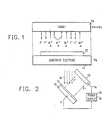
- FIG. 1illustrates the process of the present invention wherein a target 10 is held at a negative potential V T which is measured with respect to the walls of the sputtering chamber (substantially ground).
- a sputtering gascomprising, substantially, argon ions (Ar + ) impinges upon the target 10 to release negative ions therefrom.
- the sputtering gasincludes not only the traditionally used inert gases Ar, Ne, Kr, etc., but also hydrogen.
- the hydrogenis introduced into the sputtering gas as either H 2 , or as a material which will yield hydrogen.
- water vapor and other compounds of hydrogen, preferably gaseous onescan be used for this purpose.
- the presence of hydrogen in the gas used to sputter negative ions from target 10dramatically affects the etch rates achieved in a negative ion etching process.
- the negative ions released from the target 10, indicated by the arrows F-,are accelerated to the full fall potential (the potential between the negative target and the sputtering gas plasma) to a substrate 12 which is to be etched.
- the negative ionswill often lose electrons in the sputtering gas plasma and strike substrate 12 as energetic neutral particles.
- Substrate 12is located on a substrate electrode 14, which can have a small negative bias voltage V B , measured with respect to the chamber wall.
- negative ions and/or energetic neutral particlesare used for etching the substrate 12.
- Positive ionscan be prevented from reaching substrate 12 in accordance with the teachings of aforementioned U.S.-A-4,250,009.
- Substrate 12can be comprised of any material that it is to be etched, including metals, insulators, and semiconductors. Particular examples will be described with respect to Si, Si0 2 , Si 3 N 4 , and AI z 0 3 . In the practice of this invention, it has been found that the presence of hydrogen in the sputtering gas plasma causes dramatic changes in the relative etch rates of the substrate materials, without any accompanying adverse effects.
- the voltage V Tis a negative voltage for the purpose of attracting positive sputtering gas atoms from the plasma to the target, to cause release of negative ions therefrom.
- a typical range of V Tis from about -250V to about -5000 or more volts (with respect to ground).
- the sputtering ionsproduce events at the target which result in the release of these negative ions, which are then extracted by the electric field between the target and the plasma.
- the bias voltage V Bis also a negative voltage with respect to ground, and typically is about -25V to -several hundred volts. It is also of a smaller magnitude than V T . Voltage V, is used to inject electrons into the plasma, thereby enhancing ionization, and thereby also enhancing sputtering of the target.
- the hydrogen in the sputtering gasis present in an amount ranging from a few percent to about 50-75 percent, by volume. If the hydrogen is present in too small an amount, the effect on etch rates is very small while, if there is an excessive amount of hydrogen, for example in excess of 80% by volume, sputtering of the target will diminish by a large amount.
- the targetis at an angle to the direction of the energetic particle beam 16 used to sputter negative ions from target 10.
- Beam 16is produced by known apparatus, as described in U.S. 4,250,009.
- Substrate 10is located on a substrate holder (electrode 18) which is connected to a power supply 20, providing the voltage V T .
- Power supply 20is also connected to substrate 12 to provide the substrate bias V e .
- Energetic particle beam 16is used to sputter negative ions from the target 10, and contains hydrogen in order to provide selective etching of the substrate.
- Beam 16can be comprised of energetic particles such as accelerated Ar + atoms, neutrons, ions, and other particles including combinations of atoms and other subatomic particles, such as Ar + ions or the like.
- Neutral beams 16are often preferred because they do not generate high electrical currents at the target 10.
- an ion beam containing electronsit is often necessary to use means, such as a wire mesh grid, in front of the target to prevent drawing high electrical currents. This is also described in U.S.-A-4,250,009.
- the introduction of the sputtering gasargon.
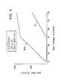
- Figs. 3, 4 and 5are various plots of the etch rates of Si and Si0 2 vs. bias voltage (FIGS. 3 and 4) and substrate temperature (FIG. 5). These curves illustrate the effect of the introduction of hydrogen into the sputtering gas and illustrate the striking differentials in etch rates that occur. The data upon which these curves are based is contained in the following table:
- the targetwas MgF 2 .
- Backed substratescontained a backing of Gain to provide heat dissipation.
- This targethad a three inch diameter and was shielded to provide a two inch opening for the sputtering plasma.
- a Mo substrate holderhad holes therein filled with Si0 2 /Si substrate.
- the target voltage V Twas -2500V and Argon at a pressure of 4 pascals (30 microns hg) was used as the sputtering gas.
- the substrateswere not backed. No hydrogen was introduced into the sputtering gas. From these curves, it is apparent that the etch rates of both Si and Si0 2 increase as the bias voltage V B becomes more negative.
- FIG. 4illustrates the situation in which three microns of hydrogen are present in the sputtering gas stream. Again, the substrates are non-backed. As is apparent from FIG. 4, the etch rate of Si decreases much more rapidly than the etch rate of Si0 2 when this amount of hydrogen is present. Thus, the etch rate ratio SiO 2 /Si is dramatically changed. In fact, the etch rate ratio Si0 2 /Si is about 2/1 without the hydrogen. With 10% hydrogen added to argon, the ratio is almost infinite.
- the etch rate of hot films of Siis reduced from 930 to 84 ⁇ /min, with the introduction of 10% hydrogen, while the etch rate of hot films of Si0 2 is increased from 1900 to 2300 A/min.
- the relative etch rate ratio of Si 3 N 4 %Siis decreased from 780 to 57 A/min, for hot films.
- the addition of 10% hydrogencauses the etch rate of silicon to be reduced to approximately 0, while the etch rate of Si0 2 is decreased 2300 to 1300 ⁇ /min.
- the etch rate ratio Si 3 N 4 /Siis approximately 0.
- a semiconductor devicecomprising layers of silicon (Si), silicon dioxide (Si0 2 ), and silicon nitride (Si 3 N 4 ) was etched.
- the etch rate SiO 2 /Siis about 2/1 in the absence of hydrogen.
- SiO 2 /Siis about 2/1 in the absence of hydrogen.
- Si 3 N 4was etched while it was not etched with a 10% hydrogen addition to the argon sputtering gas.
- the processproduces extreme etch rate differentials between these different materials.
- the presence of hydrogen in the sputtering gascauses visually observable effects.
- the plasmabecomes more brilliant, indicating a higher negative ion yield, such as F-and possibly (HF-) in the case of MgF 2 targets.
- the number of secondary electrons emitted from the targetappeared to increase, causing further enhancement of the plasma.
Landscapes
- Engineering & Computer Science (AREA)
- Physics & Mathematics (AREA)
- Plasma & Fusion (AREA)
- Condensed Matter Physics & Semiconductors (AREA)
- General Physics & Mathematics (AREA)
- Manufacturing & Machinery (AREA)
- Computer Hardware Design (AREA)
- Microelectronics & Electronic Packaging (AREA)
- Power Engineering (AREA)
- Drying Of Semiconductors (AREA)
- Physical Deposition Of Substances That Are Components Of Semiconductor Devices (AREA)
Description
- This invention relates to a negative ion beam etching process.
- Many different techniques are used to etch materials, such techniques having particular importance in the fabrication of micro-electronic devices including semiconductor devices. Those etching methods use ion beams, neutral atoms, reactive gases, etc. for the removal of layers of different materials, including metals, insulators and semiconductors.
- Negative ions have been found in low discharge sputtering systems and have been used to produce etched substrates by physical sputtering processes, as described in US―A―4,132,614 and 4,250,009. In this type of negative ion sputtering process, a highly ionic target is struck by an energetic particle, such as argon atoms, neutrons, ions, or other particles to produce negative ions which are then accelerated to a sample to be etched. The ionic targets are typically compounds which will release negative ion species such as F, Cl, Br, and I. Since the target is at a negative potential and the plasma surrounding the target is at approximately ground potential, the negative ions from the target will be accelerated by the fall potential (the potential between the negative target and the plasma) to impinge upon the sample (substrate) in order to etch it. Although the negative ion may lose electrons in the plasma, it will be sufficiently accelerated to strike the substrate as an energetic neutral particle.
- Aforementioned US-A-4,132,614 and 4,250,009 describe a negative ion etching process and the different types of apparatus used to practice that process. Additionally, reference is made to J. J. Hanak, et al, "Effect of Secondary Electrons and Negative Ions on Sputtering of Films", J. Vac. Sci. Tech., Vol. 13, pp 406―409 (1976), describing an etching process using fluoride negative ions that were generated during sputtering from a TbF3 target
- Since negative ion etching has advantages in the etching of various materials, it would be desirable to be able to control that process in order to provide the selective etching. For example, in the fabrication of semiconductor devices, it is often advantageous to have Si02 etch at a much more rapid rate than Si. Further, Si3N4 may also be found on the semiconductor devices and advantages result when Si3N4 has a different etch rate from those of Si and Si02. Heretofore, no good way has been taught or suggested for controlling the relative etch rate of different materials in a negative ion etching system.
- A negative ion beam etching process comprising plasma sputtering negative ions from a target and accelerating the negative ions to a substrate to cause etching thereof, is characterised, according to the invention, by the plasma containing hydrogen or a hydrogen compound in order to modify the etch-rate of the substrate.
- The presence of hydrogen produces a significant effect on the etch rates of different materials in this negative ion etching system.
- How the invention can be carried out will now be described by way of example, with reference to the accompanying drawings, in which:-
- FIG. 1 schematically illustrates a negative ion etching process according to the invention, in which the substrate is aligned substantially parallel to the target providing the negative etching ions;
- FIG. 2 schematically illustrates another etching process according to the invention, in which the target providing the negative etching ions is disposed at an angle to the beam used to sputter negative ions from the target;
- FIG. 3 is a plot of the etch rate of Si and Si02 vs. bias voltage, for etching of these materials without the presence of hydrogen in the sputtering gas;
- FIG. 4 is a plot of the etch rate of Si and Si02 as a function of bias voltage when hydrogen is present in the sputtering gas; and
- FIG. 5 is a plot of the etch rates of Si and Si02 vs substrate temperature, for a situation in which hydrogen is not present in the sputtering gas and for a situation in which hydrogen is present in the sputtering gas.
- In this description, referenced will be made to aforementioned US-A-4,132,614 and 4,250,009. These patents describe negative ion etching processes and suitable apparatus for these processes. Reference is also made to the previously mentioned Hanak et al article and to the references cited by Hanak et al, particularly those to Honig (Refs. 3, 4). These patents and those referenced articles describe techniques for producing negative ions. The present invention uses the teachings of those patents and technical journal articles for the formation of negative ions, where those negative ions are produced by sputtering from a suitable target providing the negative ions. A particular example is the use of an ionic compound target which will yield negative ions of F, Cl, Br, and 1.
- FIG. 1 illustrates the process of the present invention wherein a
target 10 is held at a negative potential VT which is measured with respect to the walls of the sputtering chamber (substantially ground). A sputtering gas comprising, substantially, argon ions (Ar+) impinges upon thetarget 10 to release negative ions therefrom. In the present invention, the sputtering gas includes not only the traditionally used inert gases Ar, Ne, Kr, etc., but also hydrogen. The hydrogen is introduced into the sputtering gas as either H2, or as a material which will yield hydrogen. For example, water vapor and other compounds of hydrogen, preferably gaseous ones, can be used for this purpose. As will become apparent, the presence of hydrogen in the gas used to sputter negative ions fromtarget 10 dramatically affects the etch rates achieved in a negative ion etching process. - The negative ions released from the
target 10, indicated by the arrows F-, are accelerated to the full fall potential (the potential between the negative target and the sputtering gas plasma) to asubstrate 12 which is to be etched. The negative ions will often lose electrons in the sputtering gas plasma andstrike substrate 12 as energetic neutral particles.Substrate 12 is located on asubstrate electrode 14, which can have a small negative bias voltage VB, measured with respect to the chamber wall. - In this process, negative ions and/or energetic neutral particles are used for etching the
substrate 12. Positive ions can be prevented from reachingsubstrate 12 in accordance with the teachings of aforementioned U.S.-A-4,250,009. Substrate 12 can be comprised of any material that it is to be etched, including metals, insulators, and semiconductors. Particular examples will be described with respect to Si, Si02, Si3N4, andAI z03. In the practice of this invention, it has been found that the presence of hydrogen in the sputtering gas plasma causes dramatic changes in the relative etch rates of the substrate materials, without any accompanying adverse effects.- The voltage VT is a negative voltage for the purpose of attracting positive sputtering gas atoms from the plasma to the target, to cause release of negative ions therefrom. A typical range of VT is from about -250V to about -5000 or more volts (with respect to ground). The sputtering ions produce events at the target which result in the release of these negative ions, which are then extracted by the electric field between the target and the plasma.
- The bias voltage VB is also a negative voltage with respect to ground, and typically is about -25V to -several hundred volts. It is also of a smaller magnitude than VT. Voltage V, is used to inject electrons into the plasma, thereby enhancing ionization, and thereby also enhancing sputtering of the target.
- The hydrogen in the sputtering gas is present in an amount ranging from a few percent to about 50-75 percent, by volume. If the hydrogen is present in too small an amount, the effect on etch rates is very small while, if there is an excessive amount of hydrogen, for example in excess of 80% by volume, sputtering of the target will diminish by a large amount.
- In FIG. 2, the target is at an angle to the direction of the
energetic particle beam 16 used to sputter negative ions fromtarget 10. Beam 16 is produced by known apparatus, as described in U.S. 4,250,009.Substrate 10 is located on a substrate holder (electrode 18) which is connected to apower supply 20, providing the voltage VT. Power supply 20 is also connected tosubstrate 12 to provide the substrate bias Ve. Whenbeam 16 strikestarget 10, negative ions will be released and accelerated towardssubstrate 12, as indicated by the arrows F-. Energetic particle beam 16 is used to sputter negative ions from thetarget 10, and contains hydrogen in order to provide selective etching of the substrate.Beam 16 can be comprised of energetic particles such as accelerated Ar+ atoms, neutrons, ions, and other particles including combinations of atoms and other subatomic particles, such as Ar+ ions or the like.Neutral beams 16 are often preferred because they do not generate high electrical currents at thetarget 10. When an ion beam containing electrons is used, it is often necessary to use means, such as a wire mesh grid, in front of the target to prevent drawing high electrical currents. This is also described in U.S.-A-4,250,009. The introduction of the sputtering gas (argon. etc.) is in accordance with the teaching of aforementioned patents U.S.-A-4,132,614 and 4,250,009. In the practice of the present invention, hydrogen or a species containing hydrogen is also introduced with the sputtering gas. The pressures, voltages, apparatus etc., described herein and in those patents can be used in the practice of the present invention.- Figs. 3, 4 and 5 are various plots of the etch rates of Si and Si02 vs. bias voltage (FIGS. 3 and 4) and substrate temperature (FIG. 5). These curves illustrate the effect of the introduction of hydrogen into the sputtering gas and illustrate the striking differentials in etch rates that occur. The data upon which these curves are based is contained in the following table:

- For the data of the table, the target was MgF2. Backed substrates contained a backing of Gain to provide heat dissipation. This target had a three inch diameter and was shielded to provide a two inch opening for the sputtering plasma. A Mo substrate holder had holes therein filled with Si02/Si substrate.
- In FIG. 3, the target voltage VT was -2500V and Argon at a pressure of 4 pascals (30 microns hg) was used as the sputtering gas. The substrates were not backed. No hydrogen was introduced into the sputtering gas. From these curves, it is apparent that the etch rates of both Si and Si02 increase as the bias voltage VB becomes more negative.
- FIG. 4 illustrates the situation in which three microns of hydrogen are present in the sputtering gas stream. Again, the substrates are non-backed. As is apparent from FIG. 4, the etch rate of Si decreases much more rapidly than the etch rate of Si02 when this amount of hydrogen is present. Thus, the etch rate ratio SiO2/Si is dramatically changed. In fact, the etch rate ratio Si02/Si is about 2/1 without the hydrogen. With 10% hydrogen added to argon, the ratio is almost infinite.
- FIG. 5 plots the etch rates of Si and Si02 as a function of substrate temperature for the situation when no hydrogen is present and when 10% hydrogen is introduced into the argon. For these curves, VT= -2500V, while VB= -150V. Interestingly, the etch rate of Si02 as a function of substrate temperature changes slope when hydrogen is present with the argon gas. At higher temperatures, slight etching of Si was observed. As will be described later, Si3N4 becomes unetched in the presence of 10% hydrogen, an effect which is also observed when the substrates are at high temperatures.

- Studies were also made of the etching of Si3N4 and AI203 (sapphire) in this etching apparatus. These results are illustrated in TABLE II.

- It is observed that the etch rate of hot films of Si is reduced from 930 to 84 Å/min, with the introduction of 10% hydrogen, while the etch rate of hot films of Si02 is increased from 1900 to 2300 A/min. The relative etch rate ratio of Si3N4%Si is decreased from 780 to 57 A/min, for hot films.
- For low temperature films, the addition of 10% hydrogen causes the etch rate of silicon to be reduced to approximately 0, while the etch rate of Si02 is decreased 2300 to 1300 Å/min. The etch rate ratio Si3N4/Si is approximately 0. Some data was obtained for the introduction of 10% oxygen to the system. The presence of oxygen often affected the etch rates of these materials.
- In a particular example, a semiconductor device comprising layers of silicon (Si), silicon dioxide (Si02), and silicon nitride (Si3N4) was etched. The etch rate SiO2/Si is about 2/1 in the absence of hydrogen. With a 10% hydrogen addition to an argon sputtering gas, the etch rate of Si02 decreased by about 1/3, while the etch rate of Si is decreased to 0 A/min. In the absence of hydrogen, Si3N4 was etched while it was not etched with a 10% hydrogen addition to the argon sputtering gas. Thus, the process produces extreme etch rate differentials between these different materials.
- In the practice of this invention, the presence of hydrogen in the sputtering gas causes visually observable effects. The plasma becomes more brilliant, indicating a higher negative ion yield, such as F-and possibly (HF-) in the case of MgF2 targets. Also, the number of secondary electrons emitted from the target appeared to increase, causing further enhancement of the plasma. These effects participate to produce the large effects on etch rates which are observed in this negative ion etching process.


Claims (11)
Applications Claiming Priority (2)
| Application Number | Priority Date | Filing Date | Title |
|---|---|---|---|
| US393838 | 1982-06-30 | ||
| US06/393,838US4414069A (en) | 1982-06-30 | 1982-06-30 | Negative ion beam selective etching process |
Publications (2)
| Publication Number | Publication Date |
|---|---|
| EP0098935A1 EP0098935A1 (en) | 1984-01-25 |
| EP0098935B1true EP0098935B1 (en) | 1986-03-26 |
Family
ID=23556447
Family Applications (1)
| Application Number | Title | Priority Date | Filing Date |
|---|---|---|---|
| EP83104579AExpiredEP0098935B1 (en) | 1982-06-30 | 1983-05-10 | Negative ion beam etching process |
Country Status (4)
| Country | Link |
|---|---|
| US (1) | US4414069A (en) |
| EP (1) | EP0098935B1 (en) |
| JP (1) | JPH06105700B2 (en) |
| DE (1) | DE3362664D1 (en) |
Families Citing this family (16)
| Publication number | Priority date | Publication date | Assignee | Title |
|---|---|---|---|---|
| US4778562A (en)* | 1984-08-13 | 1988-10-18 | General Motors Corporation | Reactive ion etching of tin oxide films using neutral reactant gas containing hydrogen |
| US4544444A (en)* | 1984-08-15 | 1985-10-01 | General Motors Corporation | Reactive ion etching of tin oxide films using silicon tetrachloride reactant gas |
| US4620898A (en)* | 1985-09-13 | 1986-11-04 | The United States Of America As Represented By The Administrator Of The National Aeronautics And Space Administration | Ion beam sputter etching |
| US6942764B1 (en)* | 1995-08-24 | 2005-09-13 | Taiwan Semiconductor Manufacturing Company, Ltd. | Arc-sprayed shield for pre-sputter etching chamber |
| WO2007049402A1 (en)* | 2005-10-26 | 2007-05-03 | Sharp Kabushiki Kaisha | Process for producing film using atmospheric pressure hydrogen plasma, and method and apparatus for producing purification film |
| US7416989B1 (en) | 2006-06-30 | 2008-08-26 | Novellus Systems, Inc. | Adsorption based material removal process |
| US7977249B1 (en) | 2007-03-07 | 2011-07-12 | Novellus Systems, Inc. | Methods for removing silicon nitride and other materials during fabrication of contacts |
| US8187486B1 (en) | 2007-12-13 | 2012-05-29 | Novellus Systems, Inc. | Modulating etch selectivity and etch rate of silicon nitride thin films |
| US7981763B1 (en)* | 2008-08-15 | 2011-07-19 | Novellus Systems, Inc. | Atomic layer removal for high aspect ratio gapfill |
| US8058179B1 (en) | 2008-12-23 | 2011-11-15 | Novellus Systems, Inc. | Atomic layer removal process with higher etch amount |
| US9431268B2 (en) | 2015-01-05 | 2016-08-30 | Lam Research Corporation | Isotropic atomic layer etch for silicon and germanium oxides |
| US9425041B2 (en) | 2015-01-06 | 2016-08-23 | Lam Research Corporation | Isotropic atomic layer etch for silicon oxides using no activation |
| WO2019226341A1 (en) | 2018-05-25 | 2019-11-28 | Lam Research Corporation | Thermal atomic layer etch with rapid temperature cycling |
| JP7461923B2 (en) | 2018-07-09 | 2024-04-04 | ラム リサーチ コーポレーション | Electron-excited atomic layer etching |
| US11887814B2 (en)* | 2020-02-10 | 2024-01-30 | Hitachi High-Tech Corporation | Plasma processing method |
| JP7739434B2 (en) | 2021-02-03 | 2025-09-16 | ラム リサーチ コーポレーション | Control of etching selectivity in atomic layer etching |
Family Cites Families (5)
| Publication number | Priority date | Publication date | Assignee | Title |
|---|---|---|---|---|
| IT1052390B (en)* | 1975-11-24 | 1981-06-20 | Selenia Ind Elettroniche | IMPROVEMENT IN THE MANUFACTURING PROCEDURES OF SEMICONDUCTOR DEVICES, IN PARTICULAR ENGRAVING FOR IONIC EROSION |
| US4132614A (en)* | 1977-10-26 | 1979-01-02 | International Business Machines Corporation | Etching by sputtering from an intermetallic target to form negative metallic ions which produce etching of a juxtaposed substrate |
| US4250009A (en)* | 1979-05-18 | 1981-02-10 | International Business Machines Corporation | Energetic particle beam deposition system |
| JPS5651578A (en)* | 1979-10-01 | 1981-05-09 | Toshiba Corp | Plasma etching method |
| JPS56100421A (en)* | 1980-01-17 | 1981-08-12 | Toshiba Corp | Plasma etching method |
- 1982
- 1982-06-30USUS06/393,838patent/US4414069A/ennot_activeExpired - Lifetime
- 1983
- 1983-05-10EPEP83104579Apatent/EP0098935B1/ennot_activeExpired
- 1983-05-10DEDE8383104579Tpatent/DE3362664D1/ennot_activeExpired
- 1983-05-13JPJP58082856Apatent/JPH06105700B2/ennot_activeExpired - Lifetime
Also Published As
| Publication number | Publication date |
|---|---|
| JPH06105700B2 (en) | 1994-12-21 |
| US4414069A (en) | 1983-11-08 |
| EP0098935A1 (en) | 1984-01-25 |
| DE3362664D1 (en) | 1986-04-30 |
| JPS599925A (en) | 1984-01-19 |
Similar Documents
| Publication | Publication Date | Title |
|---|---|---|
| EP0098935B1 (en) | Negative ion beam etching process | |
| US4259145A (en) | Ion source for reactive ion etching | |
| US3472751A (en) | Method and apparatus for forming deposits on a substrate by cathode sputtering using a focussed ion beam | |
| US4521286A (en) | Hollow cathode sputter etcher | |
| KR102044913B1 (en) | Method for generating ion beam having gallium ion and apparatus therefor | |
| JPH0635323B2 (en) | Surface treatment method | |
| US4716340A (en) | Pre-ionization aided sputter gun | |
| JP2001007041A (en) | Method and apparatus for removing contaminated surface in ion-implantation system | |
| EP0203573B1 (en) | Electron beam-excited ion beam source | |
| Williams | Vacuum coating with a hollow cathode source | |
| Chapman et al. | Electron effects in sputtering and cosputtering | |
| Fancey et al. | Metal clusters in ion plating | |
| US4902647A (en) | Surface modification using low energy ground state ion beams | |
| US6682634B1 (en) | Apparatus for sputter deposition | |
| JP2849771B2 (en) | Sputter type ion source | |
| EP0360994B1 (en) | Apparatus and method for producing diamond films at low temperatures | |
| JPH11238485A (en) | Ion implanting method | |
| Waldorf et al. | Generation of surface layers and microstructures with a low enery plasma beam source | |
| JPS5992995A (en) | Method for forming silicide film of high-melting metal | |
| Seki et al. | High-speed Processing with Cluster Ion Beams | |
| Matsuo et al. | Novel analysis techniques using cluster ion beams | |
| Takeuchi et al. | A compact ion source using a hollow cathode discharge and its application to thin film formation | |
| Van Bommel et al. | A STUDY OF THE H PRODUCTION ON POLY-AND MONOCRYSTALLINE CONVERTERS IN A SURFACE PLASMA SOURCE. | |
| JPS6348933Y2 (en) | ||
| Ishikawa et al. | Neutral and ionized alkaline metal bombardment type heavy negative ion source (NIABNIS) |
Legal Events
| Date | Code | Title | Description |
|---|---|---|---|
| PUAI | Public reference made under article 153(3) epc to a published international application that has entered the european phase | Free format text:ORIGINAL CODE: 0009012 | |
| AK | Designated contracting states | Designated state(s):DE FR GB | |
| 17P | Request for examination filed | Effective date:19840426 | |
| GRAA | (expected) grant | Free format text:ORIGINAL CODE: 0009210 | |
| AK | Designated contracting states | Kind code of ref document:B1 Designated state(s):DE FR GB | |
| ET | Fr: translation filed | ||
| REF | Corresponds to: | Ref document number:3362664 Country of ref document:DE Date of ref document:19860430 | |
| PLBE | No opposition filed within time limit | Free format text:ORIGINAL CODE: 0009261 | |
| STAA | Information on the status of an ep patent application or granted ep patent | Free format text:STATUS: NO OPPOSITION FILED WITHIN TIME LIMIT | |
| 26N | No opposition filed | ||
| PGFP | Annual fee paid to national office [announced via postgrant information from national office to epo] | Ref country code:GB Payment date:19930427 Year of fee payment:11 | |
| PGFP | Annual fee paid to national office [announced via postgrant information from national office to epo] | Ref country code:DE Payment date:19930525 Year of fee payment:11 | |
| PGFP | Annual fee paid to national office [announced via postgrant information from national office to epo] | Ref country code:FR Payment date:19940427 Year of fee payment:12 | |
| PG25 | Lapsed in a contracting state [announced via postgrant information from national office to epo] | Ref country code:GB Effective date:19940510 | |
| GBPC | Gb: european patent ceased through non-payment of renewal fee | Effective date:19940510 | |
| PG25 | Lapsed in a contracting state [announced via postgrant information from national office to epo] | Ref country code:DE Effective date:19950201 | |
| PG25 | Lapsed in a contracting state [announced via postgrant information from national office to epo] | Ref country code:FR Effective date:19960229 | |
| REG | Reference to a national code | Ref country code:FR Ref legal event code:ST | |
| REG | Reference to a national code | Ref country code:FR Ref legal event code:ST |