EP0098460B1 - Control device for an electrical actuator - Google Patents
Control device for an electrical actuatorDownload PDFInfo
- Publication number
- EP0098460B1 EP0098460B1EP83106087AEP83106087AEP0098460B1EP 0098460 B1EP0098460 B1EP 0098460B1EP 83106087 AEP83106087 AEP 83106087AEP 83106087 AEP83106087 AEP 83106087AEP 0098460 B1EP0098460 B1EP 0098460B1
- Authority
- EP
- European Patent Office
- Prior art keywords
- current
- control device
- control
- resistor
- comparator
- Prior art date
- Legal status (The legal status is an assumption and is not a legal conclusion. Google has not performed a legal analysis and makes no representation as to the accuracy of the status listed.)
- Expired
Links
- 239000003990capacitorSubstances0.000description4
- 238000009499grossingMethods0.000description3
- 239000004065semiconductorSubstances0.000description3
- 230000007423decreaseEffects0.000description2
- 230000001939inductive effectEffects0.000description2
- 230000001681protective effectEffects0.000description2
- 230000033228biological regulationEffects0.000description1
- 238000011161developmentMethods0.000description1
- 230000018109developmental processEffects0.000description1
Images
Classifications
- G—PHYSICS
- G05—CONTROLLING; REGULATING
- G05B—CONTROL OR REGULATING SYSTEMS IN GENERAL; FUNCTIONAL ELEMENTS OF SUCH SYSTEMS; MONITORING OR TESTING ARRANGEMENTS FOR SUCH SYSTEMS OR ELEMENTS
- G05B11/00—Automatic controllers
- G05B11/01—Automatic controllers electric
- G05B11/26—Automatic controllers electric in which the output signal is a pulse-train
Definitions
- the inventionis based on a control device according to the preamble of patent claim 1.
- GB-A-2015841is a An horrschal- do g for an inductive actuator in which a ram means of an electromagnet is movable.
- the control circuitcomprises a comparator, to which an analog control signal is supplied which represents the working state of an element actuated by the plunger.
- the control circuitfurther comprises an amplifier circuit with an output amplifier in the form of an output transistor which supplies the control current for the inductive actuator in accordance with the output signal of the comparator.
- the drive circuitfurther comprises a resistor in the positive feedback branch, which is connected to the output connection of the comparator and to one of its input connections, to which the analog control signal is present, and a resistor in the negative feedback branch, which is connected to the output of the output amplifier circuit and a further input of the comparator is switched and in this way influences the on or off state of the output.
- the control device according to the invention with the characterizing features of the main claimhas the advantage of satisfying the requirements of high current accuracy with large tolerances of the actuator as well as the control with low power loss to a large extent and at the same time getting along with a small number of components.
- This control devicecan be controlled directly, in particular by an NMOS computer unit.
- the measures listed in the subclaimspermit advantageous developments and improvements of the control device specified in the main claim.
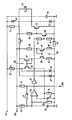
- a terminal 10 connected to the positive pole of a supply voltage sourceis connected to ground via the series connection of a low-resistance resistor 11 (e.g. 0.15 ohm) to an electrical actuator 12 and the switching path of an output stage transistor 13.
- a freewheeling diode 14is connected in parallel with the resistor 11 and the actuator 12.
- a smoothing capacitor 15 for the power circuitis connected between the terminal 10 and ground.
- a protective diode 16is connected in parallel with the switching path of transistor 13.
- a current mirror circuitis usually understood to mean the interconnection of two semiconductor elements in such a way that a current through one semiconductor element results in a corresponding or proportional current through the other semiconductor element (current path). If two transistors are used for a current mirror circuit, the two switching paths of the transistors form the two current paths, the base of one transistor is connected to the base of the other transistor and this base connection is connected to the collector of the transistor, the collector-emitter current of which another transistor to be impressed.
- the two current mirror circuits 18, 20 used hereare made up of transistors which form the current paths.
- a further series circuitwhich consists of an adjustable resistor 22 used as a setpoint generator, the second current path 23, the first current mirror circuit 18 and a resistor 24.
- a smoothing capacitor 25is connected in parallel with the resistor 24.
- the node of the resistor 24 with the current path 23is connected to the inverting input of a comparator 26.
- the non-inverting input of this comparator 26is connected to the tap of a voltage divider consisting of two resistors 27, 28, which is connected between ground and a terminal 29.
- Terminal 29is connected to a stabilized voltage source.
- a capacitor 30is connected in parallel with the resistor 28.
- a resistor 31 connected between the output of the comparator 26 and the non-inverting inputserves as a positive feedback branch for the comparator 26.
- the output of the comparator 26has an open collector, which is why this output is connected to the terminal 29 via a resistor 32 have to be.
- the control signal of a control stage designed in particular as a microcomputer (CPU)is fed to the output of the comparator 26, which continues to operate via the series connection of an inverter 33 with one of two resistors 34, 35 is connected to ground.
- the tap of the voltage divider 34, 35 of a preliminary-control transistoris set 36, whose emitter is connected to ground and its collector to the base of the output transistor 13 and through a resistor 37 to the terminal 29 to the base.
- a further series circuitis arranged between the terminal 29 and ground, which consists of two resistors 38, 39 forming a voltage divider and the second current path 40 of the second current mirror circuit 20.
- the two connections (emitters) of the two current paths 17, 23 facing away from groundare connected to ground via Zener diodes 41, 42.
- an isolating resistor 43is connected between the ground connections of the two parts.
- the non-inverting input of the comparatoris supplied with a fixed voltage, which is specified by the voltage divider 27, 28.
- the resistor 31defines the switching hysteresis in the positive feedback branch. If the current through the actuator 12 rises to such an extent that the upper switching shaft of the comparator 26 is reached, the output stage transistor 36 is switched off via the inverter 33 and the output stage transistor 36. The current through the actuator then decreases continuously in the freewheeling circuit 11, 12, 14. Since the resistor 11 is located in this freewheeling circuit, this current decrease is communicated to the inverting input of the comparator 26 via the current mirror circuit 18. When the lower switching threshold is reached, the comparator 26 therefore switches over and thus the transistor 13 again.
- the current adjustmentthat is to say the setting of a desired value, can take place by varying the resistor 22.
- Regulationtakes place only if a 1 signal (5 volts) is fed to the output of the comparator 26 via the CPU output. Due to the open collector of the output of the comparator 26, this 1 signal can be pressed onto a 0 signal depending on the switching state of the comparator 26. If, on the other hand, the CPU sends a 0 signal to the output of comparator 26, clocking can no longer take place and the control device is deactivated.
- the inverter 33can be omitted in the case of inverse switching commands. In principle, the switching signal can also be inverted by eliminating the pilot transistor 36 when the current through the actuator 12 is correspondingly low.
- the inverter 33can of course also be designed as a pilot transistor or additional pilot transistor.
- the second current mirror circuit 20the current path 40 of which is supplied with a constant current as a result of the stabilized supply voltage from the terminal 29, is used to achieve a higher current accuracy in the event of fluctuations in the supply voltage.
- Current fluctuations in the circuit 17are suppressed via the current mirroring by the current mirror circuit 20.
- the circuit shownis particularly simple and inexpensive if, for example, the transistor circuit CA 3096, which contains five transistors, is used for the five transistors 17, 23, 19, 40, 36.
- the smoothing capacitor 15 and the associated protective diode 16can, for. B. omitted in a simpler version. They serve to suppress voltage peaks in the cable compartment.
Landscapes
- Physics & Mathematics (AREA)
- General Physics & Mathematics (AREA)
- Engineering & Computer Science (AREA)
- Automation & Control Theory (AREA)
- Electronic Switches (AREA)
- Feedback Control In General (AREA)
- Amplifiers (AREA)
- Manipulation Of Pulses (AREA)
Description
Translated fromGermanDie Erfindung geht aus von einer Regelvorrichtung nach dem Oberbegriff des Patentanspruchs 1.The invention is based on a control device according to the preamble of patent claim 1.
- Aus der GB-A-2 015 841 ist eine Ansteuerschal- tung für ein induktives Stellglied bekannt, in dem ein Stössel mittels eines Elektromagneten bewegbar ist. Die Ansteuerschaltung umfasst einen Komparator, dem ein analoges Steuersignal zugeführt wird, das den Arbeitszustand eines vom Stössel betätigten Elements repräsentiert. Die Ansteuerschaltung umfasst weiter eine Verstärkerschaltung mit einem Ausgangsverstärker in Form eines Ausgangstransistors, der den Ansteuerstrom für das induktive Stellglied entsprechend dem Ausgangssignal des Komparators liefert. Die Ansteuerschaltung umfasst weiter einen Widerstand im positiven Rückkopplungszweig, der an den Ausgangsanschluss des Komparators und an einen seiner Eingangsanschlüsse geschaltet ist, an dem das analoge Kontrollsignal anliegt, sowie einen Widerstand im negativen Rückkopplungszweig, der an den Ausgang der Ausgangsverstärkerschaltung und einen weiteren Eingang des Komparators geschaltet ist und auf diese Weise den Ein- bzw. Auszustand des Ausgangs beeinflusst.- From GB-A-2015841 is a Ansteuerschal- dog for an inductive actuator is known in which a ram means of an electromagnet is movable. The control circuit comprises a comparator, to which an analog control signal is supplied which represents the working state of an element actuated by the plunger. The control circuit further comprises an amplifier circuit with an output amplifier in the form of an output transistor which supplies the control current for the inductive actuator in accordance with the output signal of the comparator. The drive circuit further comprises a resistor in the positive feedback branch, which is connected to the output connection of the comparator and to one of its input connections, to which the analog control signal is present, and a resistor in the negative feedback branch, which is connected to the output of the output amplifier circuit and a further input of the comparator is switched and in this way influences the on or off state of the output.
Ähnliche Regelvorrichtungen sind auch aus der US-PS 3 763 645, der DE-A1-3 140 301, sowie der DE-A1-3 200 475 bekannt.Similar control devices are also known from US Pat. No. 3,763,645, DE-A1-3 140 301 and DE-A1-3 200 475.
Bei solchen Regelvorrichtungen besteht grundsätzlich das Problem, auch bei grossen Toleranzen des Stellgliedes eine hohe Stromgenauigkeit des Steuerstroms zu erreichen. Dabei sollte die Ansteuerung des Stellgliedes mit möglichst niedriger Verlustleistung erfolgen. Um solchen Forderungen nachzukommen, muss bei den bekannten Regelvorrichtungen ein hoher Aufwand mit teueren Bauelementen getrieben werden.In such control devices there is basically the problem of achieving a high current accuracy of the control current even with large tolerances of the actuator. The actuator should be controlled with the lowest possible power loss. In order to meet such requirements, a high outlay with expensive components must be made in the known control devices.
Die erfindungsgemässe Regelvorrichtung mit den kennzeichnenden Merkmalen des Hauptanspruchs hat den Vorteil, die Anforderungen einer hohen Stromgenauigkeit bei grossen Toleranzen des Stellglieds sowie die Ansteuerung bei niedriger Verlustleistung in hohem Masse zu befriedigen und gleichzeitig mit einer geringen Bauelementezahl auszukommen. Dabei ist diese Regelvorrichtung insbesondere durch eine NMOS-Rechnereinheit direkt ansteuerbar. Durch die in den Unteransprüchen aufgeführten Massnahmen' sind vorteilhafte Weiterbildungen und Verbesserungen der im Hauptanspruch angegebenen Regelvorrichtung möglich.The control device according to the invention with the characterizing features of the main claim has the advantage of satisfying the requirements of high current accuracy with large tolerances of the actuator as well as the control with low power loss to a large extent and at the same time getting along with a small number of components. This control device can be controlled directly, in particular by an NMOS computer unit. The measures listed in the subclaims permit advantageous developments and improvements of the control device specified in the main claim.
Ein Ausführungsbeispiel der Erfindung ist in der Zeichnung dargestellt und in der nachfolgenden Beschreibung näher erläutert. Die einzige Figur zeigt eine schaltungsmässige Darstellung des Ausführungsbeispiels.An embodiment of the invention is shown in the drawing and explained in more detail in the following description. The single figure shows a circuit representation of the embodiment.
Eine mit dem positiven Pol einer Versorgungsspannungsquelle verbundene Klemme 10 ist über die Reihenschaltung eines niederohmigen Widerstands 11 (z.B. 0,15 Ohm) mit einem elektrischen Stellglied 12 sowie der Schaltstrecke eines Endstufentransistors 13 mit Masse verbunden. Parallel zum Widerstand 11 und zum Stellglied 12 ist eine Freilaufdiode 14 geschaltet. Zwischen die Klemme 10 und Masse ist ein Glättungskondensator 15 für den Leistungskreis geschaltet. Parallel zur Schaltstrecke des Transistors 13 liegt eine Schutzdiode 16.A
Der Verknüpfungspunkt zwischen dem Widerstand 11 und dem Stellglied 12 ist über die Reihenschaltung eines Widerstands 9, des ersten Strompfades 17 einer ersten Stromspiegelschaltung 18, des ersten Strompfads 19 einer zweiten Stromspiegelschaltung 20 sowie eines Widerstands 21 an Masse gelegt. Unter einer Stromspiegelschaltung versteht man üblicherweise die Zusammenschaltung zweier Halbleiterelemente in der Weise, dass ein Strom durch das eine Halbleiterelement einen entsprechenden oder proportionalen Strom durch das andere Halbleiterelement (Strompfad) zur Folge hat. Werden für eine Stromspiegelschaltung zwei Transistoren verwendet, so bilden die beiden Schaltstrecken der Transistoren die beiden Strompfade, die Basis des einen Transistors ist mit der Basis des anderen Transistors verbunden und diese Basisverknüpfung ist an den Kollektor des Transistors angeschlossen, dessen Kollektor-Emitter-Strom dem anderen Transistor aufgeprägt werden soll. Die beiden hier verwendeten Stromspiegelschaltungen 18, 20 sind aus Transistoren aufgebaut, die die Strompfade bilden.The point of connection between the
Zwischen der Klemme 10 und Masse liegt eine weitere Reihenschaltung, die aus einem als Sollwertgeber verwendeten einstellbaren Widerstand 22, dem zweiten Strompfad 23, der ersten Stromspiegelschaltung 18 und einem Widerstand 24 besteht. Parallel zum Widerstand 24 ist ein Glättungskondensator 25 geschaltet. Der Verknüpfungspunkt des Widerstands 24 mit dem Strompfad 23 ist an den invertierenden Eingang eines Komparators 26 gelegt. Der nicht invertierende Eingang dieses Komparators 26 ist mit dem Abgriff eines aus zwei Widerständen 27, 28 bestehenden Spannungsteilers verbunden, der zwischen Masse und eine Klemme 29 gelegt ist. Die Klemme 29 ist dabei mit einer stabilisierten Spannungsquelle verbunden. Zum Schutz gegen Störungen der stabilisierten Spannung ist parallel zum Widerstand 28 ein Kondensator 30 geschaltet. Ein zwischen den Ausgang des Komparators 26 und den nicht invertierenden Eingang geschalteter Widerstand 31 dient als Mitkopplungszweig für den Komparator 26. Der Ausgang des Komparators 26 weist einen offenen Kollektor (open collector) auf, weswegen dieser Ausgang über einen Widerstand 32 mit der Klemme 29 verbunden sein muss.Between the
Das Steuersignal einer insbesondere als Mikrorechner (CPU) ausgebildeten Steuerstufe ist dem Ausgang des Komparators 26 zugeführt, der weiterhin über die Reihenschaltung eines Inverters 33 mit einem aus zwei Widerständen 34, 35 bestehenden Spannungsteilers an Masse gelegt ist. Der Abgriff des Spannungsteilers 34, 35 ist an die Ba- sis eines Vorsteuertransistors 36 gelegt, dessen Emitter an Masse und dessen Kollektor an die Basis des Endstufentransistors 13 sowie über einen Widerstand 37 an die Klemme 29 gelegt ist.The control signal of a control stage designed in particular as a microcomputer (CPU) is fed to the output of the
Zwischen die Klemme 29 und Masse ist eine weitere Reihenschaltung gelegt, die aus zwei einen Spannungsteiler bildenden Widerständen 38, 39 sowie dem zweiten Strompfad 40 der zweiten Stromspiegelschaltung 20 besteht.A further series circuit is arranged between the
Die beiden von Masse abgewandten Anschlüsse (Emitter) der beiden Strompfade 17, 23 sind über Z-Dioden 41, 42 mit Masse verbunden.The two connections (emitters) of the two
Um den Einfluss des hohen Spannungshubs im Leistungsteil 13 bis 16 sowie 34 bis 37 auf das Steuerteil 17 bis 33 sowie 38 bis 40 zu mindern, ist ein Trennwiderstand 43 zwischen die Masseanschlüsse der beiden Teile geschaltet.In order to reduce the influence of the high voltage swing in the
Wenn der Endstufentransistor 13 leitet, so fliesst über den Widerstand 11, das Stellglied 12 sowie die Schaltstrecke dieses Transistors 13 ein Steuerstrom. Durch die Induktivität des Stellglieds 12 steigt der Strom kontinuierlich an. In Abhängigkeit des Spannungsabfalls am Widerstand 11 fliesst ebenfalls ein Strom von diesem Widerstand 11 aus über den Widerstand 9, die beiden Strompfade 17, 19 sowie den Widerstand 21. Dieser Strom ist somit proportional zum Strom durch das Stellglied 12, also zum Strom-Istwert. Durch die Stromspiegelung in der Stromspiegelschaltung 18 fliesst ein entsprechender Strom über die Reihenschaltung der Bauteile 22, 23, 24. Die Spannung am invertierenden Eingang des Komparators 26 ist somit direkt proportional zum Strom der durch den Widerstand 11, bzw. das Stellglied 12 fliesst, d.h. zum Strom-Istwert durch das Stellglied 12. Der nicht invertierende Eingang des Komparators ist mit einer festen Spannung beaufschlagt, die durch den Spannungsteiler 27, 28 vorgegeben wird. Der Widerstand 31 legt im Mitkopplungszweig die Schalthysterese fest. Steigt der Strom durch das Stellglied 12 soweit an, dass die obere Schaltwelle des Komparators 26 erreicht ist, so wird der Endstufentransistor 36 über den Inverter 33 und den Vorstufentransistor 36 abgeschaltet. Der Strom durch das Stellglied nimmt dann kontinuierlich im Freilaufkreis 11, 12, 14 ab. Da in diesem Freilaufkreis der Widerstand 11 liegt, wird diese Stromabnahme über die Stromspiegelschaltung 18 dem invertierenden Eingang des Komparators 26 mitgeteilt. Bei Erreichung der unteren Schaltschwelle schaltet daher der Komparator 26 um und damit den Transistor 13 wieder ein.When the
Der Stromabgleich, also die Einstellung eines Sollwerts, kann durch Variation des Widerstandes 22 erfolgen.The current adjustment, that is to say the setting of a desired value, can take place by varying the
Eine Regelung erfolgt nur dann, wenn über den CPU-Ausgang dem Ausgang des Komparators 26 ein 1-Signal (5 Volt) zugeführt wird. Durch den offenen Kollektor des Ausgangs des Komparators 26 kann dieses 1-Signal in Abhängigkeit des Schaltzustands des Komparators 26 auf ein 0-Signal gedrückt werden. Wird dagegen von der CPU ein 0-Signal dem Ausgang des Komparators 26 zugeführt, so kann keine Taktung mehr erfolgen und die Regelvorrichtung ist ausser Betrieb gesetzt. Es versteht sich, dass bei inversen Schaltbefehlen der Inverter 33 entfallen kann. Ebenfalls kann prinzipiell eine Invertierung des Schaltsignals dadurch erfolgen, dass bei entsprechend geringem Strom durch das Stellglied 12 der Vorsteuertransistor 36 entfällt. Der Inverter 33 kann natürlich ebenfalls als Vorsteuertransistor bzw. zusätzlicher Vorsteuertransistor ausgebildet sein.Regulation takes place only if a 1 signal (5 volts) is fed to the output of the
Die zweite Stromspiegelschaltung 20, deren Strompfad 40 mit einem konstanten Strom infolge der stabilisierten Versorgungsspannung von der Klemme 29 beaufschlagt ist, dient zur Erreichung einer höheren Stromgenauigkeit bei Schwankungen der Versorgungsspannung. Über die Stromspiegelung durch die Stromspiegelschaltung 20 werden Stromschwankungen im Stromkreis 17-unterdrückt.The second
Da z.B. im 12-Voit-Batteriebetrieb oft Störspannungsspitzen bis zu 100 Volt auftreten können, ist ein Schutz für die Stromspiegelschaltung erforderlich. Dieser Schutz ist durch die beiden Z-Dioden 41, 42 gegeben, die Spannungsspitzen z. B. über 35 Volt kurzschliessen. Da der Strom durch den niederohmigen Widerstand 11 sehr hoch sein kann, wäre dazu eine Z-Diode 41 mit hohem zulässigen Strom erforderlich. Da solche Z-Dioden sehr teuer sind, ist der Strombegrenzungswiderstand 9 in diesen Stromkreis geschaltet. Bei der Z-Diode 42 ist dies nicht erforderlich, da eine Strombegrenzung durch den variablen Widerstand 22 erfolgt.Because e.g. Protection against the current mirror circuit is necessary in 12-Voit battery operation, which can often lead to interference voltage peaks of up to 100 volts. This protection is given by the two Z diodes 41, 42, the voltage peaks z. B. Short circuit over 35 volts. Since the current through the low-
Die aufgezeigte Schaltung wird besonders einfach und billig, wenn für die fünf Transistoren 17, 23, 19, 40, 36 beispielsweise der Transistorschaltkreis CA 3096 Verwendung findet, der fünf Transistoren enthält.The circuit shown is particularly simple and inexpensive if, for example, the transistor circuit CA 3096, which contains five transistors, is used for the five
Der Glättungskondensator 15 und die zugehörige Schutzdiode 16 können z. B. bei einer einfacheren Version entfallen. Sie dienen zur Unterdrükkung von Spannungsspitzen im Kabelraum.The smoothing
Claims (7)
Applications Claiming Priority (2)
| Application Number | Priority Date | Filing Date | Title |
|---|---|---|---|
| DE19823225157DE3225157A1 (en) | 1982-07-06 | 1982-07-06 | CONTROL DEVICE FOR AN ELECTRICAL ACTUATOR |
| DE3225157 | 1982-07-06 |
Publications (3)
| Publication Number | Publication Date |
|---|---|
| EP0098460A2 EP0098460A2 (en) | 1984-01-18 |
| EP0098460A3 EP0098460A3 (en) | 1984-08-01 |
| EP0098460B1true EP0098460B1 (en) | 1987-11-19 |
Family
ID=6167700
Family Applications (1)
| Application Number | Title | Priority Date | Filing Date |
|---|---|---|---|
| EP83106087AExpiredEP0098460B1 (en) | 1982-07-06 | 1983-06-22 | Control device for an electrical actuator |
Country Status (4)
| Country | Link |
|---|---|
| US (1) | US4496885A (en) |
| EP (1) | EP0098460B1 (en) |
| JP (1) | JPS599702A (en) |
| DE (2) | DE3225157A1 (en) |
Families Citing this family (8)
| Publication number | Priority date | Publication date | Assignee | Title |
|---|---|---|---|---|
| DE3404317A1 (en)* | 1984-02-08 | 1985-08-08 | Robert Bosch Gmbh, 7000 Stuttgart | PROTECTIVE CIRCUIT FOR DEVICES CONTROLLED BY ELECTRICAL SIGNALS |
| DE3434644A1 (en)* | 1984-09-21 | 1986-04-03 | Vdo Adolf Schindling Ag, 6000 Frankfurt | METHOD AND DEVICE FOR GENERATING A CLOCKED OPERATING VOLTAGE |
| GB8727070D0 (en)* | 1987-11-19 | 1987-12-23 | Nat Res Dev | Electrical drive circuits |
| KR930011196B1 (en)* | 1988-11-16 | 1993-11-25 | 롬 가부시끼가이샤 | Motor drive circuit |
| DE19609971A1 (en)* | 1996-03-14 | 1997-09-18 | Philips Patentverwaltung | Regulated supply voltage source |
| CN102354241B (en)* | 2011-07-29 | 2015-04-01 | 开曼群岛威睿电通股份有限公司 | Voltage/current conversion circuit |
| US20140009990A1 (en)* | 2012-07-09 | 2014-01-09 | Qualcomm Incorporated | Method and apparatus for characterizing power supply impedance for power delivery networks |
| CN104714476A (en)* | 2015-03-31 | 2015-06-17 | 宁波摩米创新工场电子科技有限公司 | Automatic control system of closed-loop machine tool |
Family Cites Families (12)
| Publication number | Priority date | Publication date | Assignee | Title |
|---|---|---|---|---|
| US3568017A (en)* | 1969-08-04 | 1971-03-02 | Voumard Machines Co Sa | Push-pull oscillator for sustaining the oscillations of a resonator |
| US3649893A (en)* | 1970-08-11 | 1972-03-14 | Allegheny Ludlum Ind Inc | Synchronized driver for electrical utilization devices |
| US3763745A (en)* | 1972-01-28 | 1973-10-09 | Chandler Evans Inc | Closed center valve control system |
| DE2612914C2 (en)* | 1976-03-26 | 1983-11-10 | Robert Bosch Gmbh, 7000 Stuttgart | Device for the current-regulated control of electromagnetic injection valves assigned to an internal combustion engine |
| US4123729A (en)* | 1977-07-22 | 1978-10-31 | General Motors Corporation | Displacement transducer |
| JPS6032327B2 (en)* | 1978-03-06 | 1985-07-27 | 自動車機器株式会社 | Electrical-mechanical converter drive circuit using solenoid coils |
| CA1101967A (en)* | 1978-07-14 | 1981-05-26 | Bata Industries Limited | Control circuit for electromagnetic apparatus |
| US4418323A (en)* | 1980-03-07 | 1983-11-29 | Pioneer Electronic Corporation | Oscillator having capacitor charged and discharged by current mirror circuits |
| US4350904A (en)* | 1980-09-22 | 1982-09-21 | Bell Telephone Laboratories, Incorporated | Current source with modified temperature coefficient |
| US4336507A (en)* | 1981-01-29 | 1982-06-22 | Motorola, Inc. | Current output relaxation oscillator |
| US4338646A (en)* | 1981-04-27 | 1982-07-06 | Motorola, Inc. | Current limiting circuit |
| US4435678A (en)* | 1982-02-26 | 1984-03-06 | Motorola, Inc. | Low voltage precision current source |
- 1982
- 1982-07-06DEDE19823225157patent/DE3225157A1/enactiveGranted
- 1983
- 1983-05-24USUS06/497,505patent/US4496885A/ennot_activeExpired - Fee Related
- 1983-06-21JPJP58110283Apatent/JPS599702A/enactiveGranted
- 1983-06-22EPEP83106087Apatent/EP0098460B1/ennot_activeExpired
- 1983-06-22DEDE8383106087Tpatent/DE3374614D1/ennot_activeExpired
Also Published As
| Publication number | Publication date |
|---|---|
| JPH0352081B2 (en) | 1991-08-08 |
| EP0098460A3 (en) | 1984-08-01 |
| EP0098460A2 (en) | 1984-01-18 |
| DE3225157A1 (en) | 1984-01-12 |
| JPS599702A (en) | 1984-01-19 |
| DE3374614D1 (en) | 1987-12-23 |
| DE3225157C2 (en) | 1990-06-07 |
| US4496885A (en) | 1985-01-29 |
Similar Documents
| Publication | Publication Date | Title |
|---|---|---|
| DE2132717A1 (en) | ACTUATION CIRCUIT FOR HIGH SWITCHING SPEED SOLENOID VALVES, IN PARTICULAR A HYDRAULIC CONTROL DEVICE | |
| DE3509714A1 (en) | COUPLING CIRCUIT AND METHOD FOR MAKING SAME | |
| EP1050965A2 (en) | Electrical circuit for driving a load | |
| EP0178446A1 (en) | Semiconductor type chopper device | |
| EP0098460B1 (en) | Control device for an electrical actuator | |
| EP0986039B1 (en) | Device for supplying power to a current loop transmitter | |
| DE3044150A1 (en) | VOLTAGE REGULATOR INTERFACE CIRCUIT | |
| DE3233536A1 (en) | DEVICE FOR THE CLOCKED REGULATION OF A COIL FLOWING THROUGH | |
| DE4403375A1 (en) | Device and method for controlling an inductive load | |
| EP0944159B1 (en) | DC-DC converter | |
| DE3626088C2 (en) | ||
| EP0141166B1 (en) | Switch arrangement for electrical tools | |
| EP0373240A1 (en) | Self regulating driver circuit with saturation level regulation for the base current of a power transistor | |
| DE2404850C3 (en) | Electronic fuse for a push-pull amplifier | |
| DE68911196T2 (en) | Operating circuit. | |
| EP1326338B1 (en) | Device for controlling an electric power component | |
| DE102015212412A1 (en) | Electronically adjustable inductive proximity switch | |
| DE2032227C3 (en) | Arrangement for speed control of a direct current motor fed by controllable semiconductors | |
| EP0698840A2 (en) | Circuit arrangement for voltage limitation | |
| EP2629419B1 (en) | Device for generating short electric impulses | |
| DE2100929A1 (en) | Control circuit for supplying an inductive consumer | |
| DE10020927C2 (en) | Circuit arrangement for limiting the current of a voltage-controlled load | |
| DE2031577C3 (en) | Circuit arrangement for controlling the speed of a direct current motor fed by controllable semiconductors, in particular thyristors | |
| DE2003587B2 (en) | Circuit arrangement for controlling the average resistance of an electronic switching element by means of pulse width modulation | |
| DE2242276C3 (en) | Series control device equipped with an electronic short-circuit and overcurrent protection |
Legal Events
| Date | Code | Title | Description |
|---|---|---|---|
| PUAI | Public reference made under article 153(3) epc to a published international application that has entered the european phase | Free format text:ORIGINAL CODE: 0009012 | |
| 17P | Request for examination filed | Effective date:19830622 | |
| AK | Designated contracting states | Designated state(s):CH DE FR GB IT LI SE | |
| PUAL | Search report despatched | Free format text:ORIGINAL CODE: 0009013 | |
| AK | Designated contracting states | Designated state(s):CH DE FR GB IT LI SE | |
| GRAA | (expected) grant | Free format text:ORIGINAL CODE: 0009210 | |
| AK | Designated contracting states | Kind code of ref document:B1 Designated state(s):CH DE FR GB IT LI SE | |
| REF | Corresponds to: | Ref document number:3374614 Country of ref document:DE Date of ref document:19871223 | |
| ET | Fr: translation filed | ||
| GBT | Gb: translation of ep patent filed (gb section 77(6)(a)/1977) | ||
| ITF | It: translation for a ep patent filed | ||
| PLBE | No opposition filed within time limit | Free format text:ORIGINAL CODE: 0009261 | |
| STAA | Information on the status of an ep patent application or granted ep patent | Free format text:STATUS: NO OPPOSITION FILED WITHIN TIME LIMIT | |
| 26N | No opposition filed | ||
| ITTA | It: last paid annual fee | ||
| PGFP | Annual fee paid to national office [announced via postgrant information from national office to epo] | Ref country code:GB Payment date:19920505 Year of fee payment:10 | |
| PGFP | Annual fee paid to national office [announced via postgrant information from national office to epo] | Ref country code:SE Payment date:19920605 Year of fee payment:10 | |
| PGFP | Annual fee paid to national office [announced via postgrant information from national office to epo] | Ref country code:FR Payment date:19920629 Year of fee payment:10 | |
| PGFP | Annual fee paid to national office [announced via postgrant information from national office to epo] | Ref country code:DE Payment date:19920825 Year of fee payment:10 | |
| PGFP | Annual fee paid to national office [announced via postgrant information from national office to epo] | Ref country code:CH Payment date:19920924 Year of fee payment:10 | |
| PG25 | Lapsed in a contracting state [announced via postgrant information from national office to epo] | Ref country code:GB Effective date:19930622 | |
| PG25 | Lapsed in a contracting state [announced via postgrant information from national office to epo] | Ref country code:SE Effective date:19930623 | |
| PG25 | Lapsed in a contracting state [announced via postgrant information from national office to epo] | Ref country code:LI Effective date:19930630 Ref country code:CH Effective date:19930630 | |
| GBPC | Gb: european patent ceased through non-payment of renewal fee | Effective date:19930622 | |
| PG25 | Lapsed in a contracting state [announced via postgrant information from national office to epo] | Ref country code:FR Effective date:19940228 | |
| REG | Reference to a national code | Ref country code:CH Ref legal event code:PL | |
| PG25 | Lapsed in a contracting state [announced via postgrant information from national office to epo] | Ref country code:DE Effective date:19940301 | |
| REG | Reference to a national code | Ref country code:FR Ref legal event code:ST | |
| EUG | Se: european patent has lapsed | Ref document number:83106087.6 Effective date:19940110 |