EP0076105B1 - Method of producing a bipolar transistor - Google Patents
Method of producing a bipolar transistorDownload PDFInfo
- Publication number
- EP0076105B1 EP0076105B1EP82305023AEP82305023AEP0076105B1EP 0076105 B1EP0076105 B1EP 0076105B1EP 82305023 AEP82305023 AEP 82305023AEP 82305023 AEP82305023 AEP 82305023AEP 0076105 B1EP0076105 B1EP 0076105B1
- Authority
- EP
- European Patent Office
- Prior art keywords
- layer
- insulating layer
- region
- base electrode
- base
- Prior art date
- Legal status (The legal status is an assumption and is not a legal conclusion. Google has not performed a legal analysis and makes no representation as to the accuracy of the status listed.)
- Expired
Links
Images


Classifications
- H—ELECTRICITY
- H10—SEMICONDUCTOR DEVICES; ELECTRIC SOLID-STATE DEVICES NOT OTHERWISE PROVIDED FOR
- H10D—INORGANIC ELECTRIC SEMICONDUCTOR DEVICES
- H10D48/00—Individual devices not covered by groups H10D1/00 - H10D44/00
- H10D48/30—Devices controlled by electric currents or voltages
- H10D48/32—Devices controlled by only the electric current supplied, or only the electric potential applied, to an electrode which does not carry the current to be rectified, amplified or switched
- H10D48/34—Bipolar devices
- H10D48/345—Bipolar transistors having ohmic electrodes on emitter-like, base-like, and collector-like regions
- H—ELECTRICITY
- H01—ELECTRIC ELEMENTS
- H01L—SEMICONDUCTOR DEVICES NOT COVERED BY CLASS H10
- H01L21/00—Processes or apparatus adapted for the manufacture or treatment of semiconductor or solid state devices or of parts thereof
- H01L21/02—Manufacture or treatment of semiconductor devices or of parts thereof
- H01L21/027—Making masks on semiconductor bodies for further photolithographic processing not provided for in group H01L21/18 or H01L21/34
- H01L21/033—Making masks on semiconductor bodies for further photolithographic processing not provided for in group H01L21/18 or H01L21/34 comprising inorganic layers
- H—ELECTRICITY
- H01—ELECTRIC ELEMENTS
- H01L—SEMICONDUCTOR DEVICES NOT COVERED BY CLASS H10
- H01L21/00—Processes or apparatus adapted for the manufacture or treatment of semiconductor or solid state devices or of parts thereof
- H01L21/02—Manufacture or treatment of semiconductor devices or of parts thereof
- H01L21/04—Manufacture or treatment of semiconductor devices or of parts thereof the devices having potential barriers, e.g. a PN junction, depletion layer or carrier concentration layer
- H01L21/18—Manufacture or treatment of semiconductor devices or of parts thereof the devices having potential barriers, e.g. a PN junction, depletion layer or carrier concentration layer the devices having semiconductor bodies comprising elements of Group IV of the Periodic Table or AIIIBV compounds with or without impurities, e.g. doping materials
- H01L21/28—Manufacture of electrodes on semiconductor bodies using processes or apparatus not provided for in groups H01L21/20 - H01L21/268
- H01L21/283—Deposition of conductive or insulating materials for electrodes conducting electric current
- H01L21/285—Deposition of conductive or insulating materials for electrodes conducting electric current from a gas or vapour, e.g. condensation
- H01L21/28506—Deposition of conductive or insulating materials for electrodes conducting electric current from a gas or vapour, e.g. condensation of conductive layers
- H01L21/28512—Deposition of conductive or insulating materials for electrodes conducting electric current from a gas or vapour, e.g. condensation of conductive layers on semiconductor bodies comprising elements of Group IV of the Periodic Table
- H—ELECTRICITY
- H10—SEMICONDUCTOR DEVICES; ELECTRIC SOLID-STATE DEVICES NOT OTHERWISE PROVIDED FOR
- H10D—INORGANIC ELECTRIC SEMICONDUCTOR DEVICES
- H10D64/00—Electrodes of devices having potential barriers
- H10D64/20—Electrodes characterised by their shapes, relative sizes or dispositions
- H10D64/27—Electrodes not carrying the current to be rectified, amplified, oscillated or switched, e.g. gates
- H10D64/281—Base electrodes for bipolar transistors
- Y—GENERAL TAGGING OF NEW TECHNOLOGICAL DEVELOPMENTS; GENERAL TAGGING OF CROSS-SECTIONAL TECHNOLOGIES SPANNING OVER SEVERAL SECTIONS OF THE IPC; TECHNICAL SUBJECTS COVERED BY FORMER USPC CROSS-REFERENCE ART COLLECTIONS [XRACs] AND DIGESTS
- Y10—TECHNICAL SUBJECTS COVERED BY FORMER USPC
- Y10S—TECHNICAL SUBJECTS COVERED BY FORMER USPC CROSS-REFERENCE ART COLLECTIONS [XRACs] AND DIGESTS
- Y10S148/00—Metal treatment
- Y10S148/01—Bipolar transistors-ion implantation
- Y—GENERAL TAGGING OF NEW TECHNOLOGICAL DEVELOPMENTS; GENERAL TAGGING OF CROSS-SECTIONAL TECHNOLOGIES SPANNING OVER SEVERAL SECTIONS OF THE IPC; TECHNICAL SUBJECTS COVERED BY FORMER USPC CROSS-REFERENCE ART COLLECTIONS [XRACs] AND DIGESTS
- Y10—TECHNICAL SUBJECTS COVERED BY FORMER USPC
- Y10S—TECHNICAL SUBJECTS COVERED BY FORMER USPC CROSS-REFERENCE ART COLLECTIONS [XRACs] AND DIGESTS
- Y10S148/00—Metal treatment
- Y10S148/04—Dopants, special
Definitions
- the present inventionrelates to a method of producing semiconductor devices. More particularly, it relates to a method of producing bipolar transistors in an integrated circuit.
- an integrated circuitcomprising bipolar transistors, i.e. a bipolar IC, denser.
- a base region and an emitter region of each of the bipolar transistorsare decreased to increase the density, the accuracy of alignment of the emitter region in relation to the base region may become a problem.
- openings for a base electrode, an emitter electrode, and a collector electrodeare simultaneously formed in an insulating layer, if the position of the openings for the electrodes is shifted from a predetermined position, a short-circuit between the emitter and collector, or a decrease in the breakdown voltage between the emitter and collector, may occur.
- an N-type silicon expitaxial layer 2is grown, as illustrated in Figure 1.
- An N +- type buried layer 3( Figure 1) for reducing the resistance of the collector is formed by a well-known process.
- An anti-oxidizing masking layer 4for example a silicon nitride (Si 3 N 4 ) layer, having a thickness of, for example, 100 nm, is formed on the epitaxial layer 2. and then is selectively removed by a photoetching process to leave portions corresponding to an isolation-providing region, a collector-providing region, and a base-providing region.
- the epitaxial layer 2is selectively thermally oxidized by using the silicon nitride layer 4 as a mask so that a relatively thick silicon dioxide (Si0 2 ) layer (i.e. a so-called field oxide layer or field insulating layer) 5 is formed, as illustrated in Figure 2.
- Si0 2silicon dioxide
- P-type impuritiese.g., boron
- P-type impuritiesare introduced into a portion of the expitaxial layer 2 by an ion-implantation process by using the field oxide layer 5 and a patterned photoresist layer (not shown) as a mask to form a P-type isolation region 6.
- N-type impurities(donor e.g., phosphorus (P)) are introduced into another portion of the expitaxial layer 2 by an ion-implantation process by using the field oxide layer 5 and another patterned photoresist layer (not shown) as another mask to form an N-type collector contact region 7. Then the obtained semiconductor body is annealed so as to activate the isolation region 6 and the collector contact region 7.
- Pphosphorus
- the silicon nitride layer 4is removed by etching to expose portions of the epitaxial layer 2.
- the exposed portionsare thermally oxidized to form a relatively thin silicon dioxide layer 8 having a thickness of e.g., 100 nm, as illustrated in Figure 3.
- a photoresist layer 9is coated, exposed, and developed to form an opening 10 above a base-providing region.
- P-type impurities(acceptor e.g., boron (B)) are introduced into the epitaxial layer 2 through the opening 10 and the silicon dioxide layer 8 by an ion-implantation process to form a base region 11.
- a silicon oxide layer 12is formed on the thick field oxide layer 5 and on the thin silicon dioxide layer 8 by a chemical vapor deposition (CVD) process, as illustrated in Figure 4.
- the oxide layers 12 and 8are selectively etched by a conventional photoetching process to form a collector electrode opening 13, an emitter electrode opening 14, and a base electrode opening 15, simultaneously.
- a polycrystalline silicon layer 16( Figure 5) having a thickness of, e.g., 100 nm is formed on the silicon oxide layer 12 and exposed portions of the epitaxial layer 2 within the openings 13, 14, and 15 by a CVD process.
- N-type impuritiese.g., arsenic (As)
- Asarsenic
- a conductive layersuch as an aluminum (AI) layer
- AIaluminum
- the aluminum layer 'is selectively etched by a conventional photoetching process to form a collector electrode 19, an emitter electrode 20, a base electrode 21, and conductive lines (not shown).
- the portion of the polycrystalline silicon layer 16 which is not covered with the electrodes 19,20, and 21 and the conductive linesis etched with a suitable etchant.
- the bipolar transistor shown in Figure 5is produced.
- the silicon oxide layers 12 and 8are selectively etched to form the openings 13, 14, and 15 for the collector electrode 19, the emitter electrode 20, and the base electrode 21, respectively, in the above-mentioned production process, there is the possibility of shifting of the position of the openings 13, 14, and 15 from the predetermined position.
- the emitter electrode opening 14is shifted to etch a portion of the thick field oxide layer 5, as illustrated in Figure 6, the emitter region 18 is formed at the end portion of the base region 11, whereby a short-circuit 22 between the collector and emitter is formed.
- a second insulating layeris formed over the polysilicon layer and thinly covers the edges of the polysilicon layer, the first insulating layer and the base electrode within the opening.
- the second insulating layeracts as a mask, within the opening, for the subsequent formation of an emitter region by introduction of impurities into the base region.
- An object of the present inventionis to provide an improved bipolar transistor.
- a method of producing a bipolar_transistor having a base region, an emitter region, and a base electrodecomprising the steps of depositing a high-melting-point metal on the base region to form the base electrode; forming a first insulating layer on the base electrode; selectively etching the. first insulating layer and the base electrode to form an opening in which a portion of the base region is exposed; forming a second insulating layer covering the edges of the base electrode and the first insulating layer within the opening; and introducing impurities into the base region by using the second insulating layer within the opening as a mask to form.
- the second insulating layeris formed with a greater thickness than the total thickness of the first insulating layer and the base electrode; and in that the second insulating layer is anisotropically dry etched to remove the major part of the second insulating layer but leaving portions of the second insulating layer covering the edge of the base electrode and the first insulating layer within the opening.
- the starting materialis a semiconductor substrate 31 being, for example, P-type single crystalline silicon.
- An N-type silicon epitaxial layer 32is grown on the silicon substrate 31.
- An N I- type buried layer 33is formed by a conventional process.
- a silicon nitride layeris formed on the epitaxial layer 32 and then is selectively etched by a conventional photoetching process to leave portions 34A, 34B, and 34C corresponding to an isolation-providing region, a collector-providing region, and a base-providing region, respectively.
- the epitaxial layer 32is selectively thermally oxidized to form a thick silicon dioxide layer (i.e., a field oxide layer) 35, as illustrated in Figure 8.
- P-type impuritiese.g., boron (B)
- B-type impuritiesare selectively introduced into the epitaxial layer 32 through the silicon nitride layer portion 34A by a conventional ion-implantation process to form a P-type isolation region 36.
- N-type impuritiese.g., phosphorus (P)
- Pphosphorus
- the above-mentioned production stepsare the same as those of the prior art mentioned in rotation to Figures 1 and 2.
- the silicon nitride layer portion 34Ais removed by a photoetching process.
- An annealing treatmentis carried out under an oxidizing atmosphere so that the silicon of the isolation region 36 is thermally oxidized to form an insulating layer 38 of silicon dioxide and, simultaneously, the doped regions 36 and 37 expand to reach the silicon substrate 31 and the buried layer 33, respectively, as illustrated in Figure 9.
- a photoresist layer 39is coated, exposed, and developed to form an opening 40 ( Figure 9) above a base-providing region.
- P-type impuritiese.g., boron
- a high-melting-point metal layer 42 for a base electrodeis formed on the exposed surfaces of the oxide layer 35 (and 38) and the base region 41 (and the collector contact region 37) by a sputtering process or a vacuum evaporation process, as illustrated in Figure 10.
- the high-melting-point metalis a metal having a melting point higher than the temperature of the heat treatments (e.g., annealing) in the production process.
- Gold (Au), molybdenum (Mo), or tungsten (W)can be used as the high-melting-point metal.
- an alloy layer of titanium-palladium (Ti-Pd) or titanium-platinum (Ti-Pt)should be formed between the epitaxial layer and the gold layer so as to prevent a reaction between the gold layer and the silicon of the epitaxial layer.
- the high-melting-point metal layer 42consists of the alloy layer and the gold layer.
- the titanium-platinum layer having a thickness of approximately 50 nmis formed on the exposed surfaces by a sputtering process and the gold layer having a thickness of approximately 400 nm is formed on the titanium-platinum layer by a vacuum evaporation process.
- a first insulating layer 43 having a thickness of, e.g., approximately 1 pmis formed by depositing phosphosilicate glass (PSG) or silicon nitride on the high-melting-point metal layer 42 by a conventional CVD process, as illustrated in Figure 10.
- PSGphosphosilicate glass
- silicon nitridesilicon nitride
- a photoresist layer 44 having a base electrode patternis formed on the first insulating layer 43, as illustrated in Figure 11.
- the first insulating layer 43is selectively etched by a suitable etching process, e.g., a sputter etching process, by using trifluoromethane (CHF 3 ) gas.
- CHF 3trifluoromethane
- the high-melting-point metal layer 42is selectively etched by using the photoresist layer 44 and/or the first insulating layer 43 as a mask to form a base electrode having an opening 45 (Figure 11).
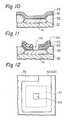
- Figure 12is a plan view of a bipolar transistor in the intermediate stage of production shown in Figure 11.
- the metal layer 42is made of molybdenum or tungsten, this layer can be etched by a sputter etching process.
- the metal layer 42consists of a gold layer and an alloy layer of titanium-palladium or titanium-platinum, the gold layer is etched by an ion-beam etching process by using argon ion-beam bombarding at right angles to the substrate and the alloy layer is etched by a wet etching process by using a suitable etching solution.
- the alloy layeris used as a stopper.
- a second insulating layer 46is formed by depositing phosphosilicate glass or silicon nitride on the exposed surface by a CVD process, as illustrated in Figure 13.
- the thickness (T) of the second insulating layer 46should be larger than the total thickness (T 1 ) of the first insulating layer 43 and the base electrode 42.
- the thickness (T 2 ) of a portion of the second insulating layer 46 near the edges of the first insulating layer 43is approximately 2 times thicker than the thickness (T) of a portion of the second insulating layer 46 on the flat surface and the inclined surface.
- the second insulating layer 46is anisotropically etched by a reactive sputter etching process by using, e.g., CHF 3 gas, or a reactive ion-beam etching process by using carbon tetrafluoride (CF 4 ) gas to form an opening 47 for defining an emitter-providing region, as illustrated in Figure 14.
- a reactive sputter etching processby using, e.g., CHF 3 gas
- CF 4carbon tetrafluoride
- a polycrystalline silicon layer 48(having a thickness of, e.g., 100 nm) on the exposed surface by a CVD process so as to prevent the reaction between emitter region and electrode metal (e.g., Al). Then a photoresist layer (not shown) serving as a mask during an ion-implantation process is formed on the polycrystalline silicon layer 48. N-type impurities (e.g., arsenic (As)) are introduced (i.e., doped) into the base region 41 through the polycrystalline silicon layer 48 by an ion-implantation process by using the photoresist layer and the first and second insulating layers 43 and 46 as a mask so that an emitter region 49 ( Figure 14) is formed.
- N-type impuritiese.g., arsenic (As)
- Asarsenic
- an N *- type region 50( Figure 15) is preferably formed in the collector contact region 37.
- annealingis carried out, for example, at 900°C for approximately 30 minutes under a dry nitrogen (N 2 ) atmosphere.
- the polycrystalline silicon layer 48has a good electric conductivity due to the introduction of N-type impurities into it.
- a metal layeris formed by depositing a metal having a good electric conductivity, such as aluminum, on the exposed surface by means of a vacuum evaporation process and is selectively etched to form an emitter electrode 51 and a collector electrode 52 by means of a photoetching process, as illustrated in Figure 15. Then the polycrystalline silicon layer 48 is also selectively etched with a suitable etchant. Thus, a bipolar transistor is produced.
- a metal having a good electric conductivitysuch as aluminum
- the opening for defining the emitter-providing regioncan be formed in approximately the middle of the base region. If the opening is shifted somewhat toward or away from the middle, the undesirable short-circuiting between the collector and emitter does not occur since the thick field oxide layer covered with the metal layer and the first insulating layer is not etched.
- the base electrode and the emitter. electrodeare formed, respectively, and are arranged in a like multilayer structure, whereby it is possible to reduce the base region area. Therefore, the density of a bipolar IC can be increased as compared with a conventional bipolar IC. Furthermore, it is possible to reduce the external base resistance and the parasitic capacity between the collector and base so that the frequency characteristic (f T ) is improved.
- a PNP-type bipolar transistorcan be produced instead of the NPN-type bipolar transistor set forth above.
- Another isolation systeme.g., dielectric isolation
- silicidee.g., MoSi 2 , WSi 2 , TiSi 2 , and the like
Landscapes
- Engineering & Computer Science (AREA)
- Physics & Mathematics (AREA)
- Condensed Matter Physics & Semiconductors (AREA)
- General Physics & Mathematics (AREA)
- Manufacturing & Machinery (AREA)
- Computer Hardware Design (AREA)
- Microelectronics & Electronic Packaging (AREA)
- Power Engineering (AREA)
- Chemical & Material Sciences (AREA)
- Inorganic Chemistry (AREA)
- Bipolar Transistors (AREA)
- Electrodes Of Semiconductors (AREA)
Description
- The present invention relates to a method of producing semiconductor devices. More particularly, it relates to a method of producing bipolar transistors in an integrated circuit.
- Recently, there have been attempts to make an integrated circuit (IC) comprising bipolar transistors, i.e. a bipolar IC, denser. When a base region and an emitter region of each of the bipolar transistors are decreased to increase the density, the accuracy of alignment of the emitter region in relation to the base region may become a problem. In a case where openings for a base electrode, an emitter electrode, and a collector electrode are simultaneously formed in an insulating layer, if the position of the openings for the electrodes is shifted from a predetermined position, a short-circuit between the emitter and collector, or a decrease in the breakdown voltage between the emitter and collector, may occur.
- A conventional method of producing a bipolar transistor will now be explained and the above-mentioned disadvantages will be explained with reference to Figures 1 to 6 of the accompanying drawings.
- On a P-type single crystalline silicon (Si) substrate (i.e. a P-type silicon wafer) 1 an N-type silicon
expitaxial layer 2 is grown, as illustrated in Figure 1. An N+-type buried layer 3 (Figure 1) for reducing the resistance of the collector is formed by a well-known process. Ananti-oxidizing masking layer 4, for example a silicon nitride (Si3N4) layer, having a thickness of, for example, 100 nm, is formed on theepitaxial layer 2. and then is selectively removed by a photoetching process to leave portions corresponding to an isolation-providing region, a collector-providing region, and a base-providing region. - The
epitaxial layer 2 is selectively thermally oxidized by using thesilicon nitride layer 4 as a mask so that a relatively thick silicon dioxide (Si02) layer (i.e. a so-called field oxide layer or field insulating layer) 5 is formed, as illustrated in Figure 2. P-type impurities (e.g., boron) are introduced into a portion of theexpitaxial layer 2 by an ion-implantation process by using thefield oxide layer 5 and a patterned photoresist layer (not shown) as a mask to form a P-type isolation region 6. N-type impurities (donor e.g., phosphorus (P)) are introduced into another portion of theexpitaxial layer 2 by an ion-implantation process by using thefield oxide layer 5 and another patterned photoresist layer (not shown) as another mask to form an N-typecollector contact region 7. Then the obtained semiconductor body is annealed so as to activate theisolation region 6 and thecollector contact region 7. - The
silicon nitride layer 4 is removed by etching to expose portions of theepitaxial layer 2. The exposed portions are thermally oxidized to form a relatively thinsilicon dioxide layer 8 having a thickness of e.g., 100 nm, as illustrated in Figure 3. A photoresist layer 9 is coated, exposed, and developed to form an opening 10 above a base-providing region. P-type impurities (acceptor e.g., boron (B)) are introduced into theepitaxial layer 2 through theopening 10 and thesilicon dioxide layer 8 by an ion-implantation process to form abase region 11. - After removal of the photoresist layer 9, a
silicon oxide layer 12 is formed on the thickfield oxide layer 5 and on the thinsilicon dioxide layer 8 by a chemical vapor deposition (CVD) process, as illustrated in Figure 4. Theoxide layers collector electrode opening 13, an emitter electrode opening 14, and a base electrode opening 15, simultaneously. - A polycrystalline silicon layer 16 (Figure 5) having a thickness of, e.g., 100 nm is formed on the
silicon oxide layer 12 and exposed portions of theepitaxial layer 2 within theopenings openings collector contact region 7 and thebase region 11 through thepolycrystalline silicon layer 16 by an ion-implantation process by using the photoresist layer as a mask so that an N*-typecollector contact region 17 and an N+-type emitter region 18 are formed, as illustrated in Figure 5. An annealing treatment is carried out and then a conductive layer, such as an aluminum (AI) layer, is formed on the exposed surface of thepolycrystalline silicon layer 16 by a vacuum evaporation. The aluminum layer'is selectively etched by a conventional photoetching process to form acollector electrode 19, anemitter electrode 20, abase electrode 21, and conductive lines (not shown). The portion of thepolycrystalline silicon layer 16 which is not covered with theelectrodes - When the
silicon oxide layers openings collector electrode 19, theemitter electrode 20, and thebase electrode 21, respectively, in the above-mentioned production process, there is the possibility of shifting of the position of theopenings emitter electrode opening 14 is shifted to etch a portion of the thickfield oxide layer 5, as illustrated in Figure 6, theemitter region 18 is formed at the end portion of thebase region 11, whereby a short-circuit 22 between the collector and emitter is formed. In a case where the degree of shift of the position of the openings is less than that of the degree of shift shown in Figure 6, if the end of the emitter region is very close to the end of the base region, the breakdown voltage between the emitter and collector is decreased. In order to prevent the above-mentioned disadvantages from occurring, it is possible to make the base region large. However, such an enlarged base region hinders an increase of the density of the bipolar IC. - An article "Bipolar transistor structure with extended metal base contacts and diffused or implanted emitter" by T. H. Ning and H. N. Yu, in IBM Technical Disclosure Bulletin,
Volume 22, No. 5, October 1979, pages 2123-2126 discloses a method of producing a bipolar transistor in which a high-melting-point metal is deposited on a base region to form a base electrode. A first insulating layer is then formed on the base electrode, a polysilicon layer is formed over the first insulating layer, and thereafter the polysilicon layer, the insulating layer and the base electrode are etched to form an opening through which a portion of the base region is exposed. A second insulating layer is formed over the polysilicon layer and thinly covers the edges of the polysilicon layer, the first insulating layer and the base electrode within the opening. The second insulating layer acts as a mask, within the opening, for the subsequent formation of an emitter region by introduction of impurities into the base region. - An object of the present invention is to provide an improved bipolar transistor.
- According .to the present invention there is provided a method of producing a bipolar_transistor having a base region, an emitter region, and a base electrode, comprising the steps of depositing a high-melting-point metal on the base region to form the base electrode; forming a first insulating layer on the base electrode; selectively etching the. first insulating layer and the base electrode to form an opening in which a portion of the base region is exposed; forming a second insulating layer covering the edges of the base electrode and the first insulating layer within the opening; and introducing impurities into the base region by using the second insulating layer within the opening as a mask to form. an emitter region; characterised in that the second insulating layer is formed with a greater thickness than the total thickness of the first insulating layer and the base electrode; and in that the second insulating layer is anisotropically dry etched to remove the major part of the second insulating layer but leaving portions of the second insulating layer covering the edge of the base electrode and the first insulating layer within the opening.
- An embodiment of the present invention will now be described, by way of example, with reference to the accompanying drawings, wherein:
- Figures 1 to 5 are schematic sectional views of a bipolar transistor in various stages of production in accordance with the prior art, as described above;
- Figure 6 is a partially enlarged sectional view of a bipolar transistor made by the method according to the prior art;
- Figures 7 through 11 are schematic sectional views of a bipolar transistor in various stages of production in accordance with the present invention;
- Figure 12 is a plan view of a bipolar transistor in the stage of production shown in Figure 11; and
- Figures 13 through 15 are schematic sectional views of a bipolar transistor made by the method in accordance with the present invention.
- In a first stage of production of a transistor shown in Figure 7, the starting material is a
semiconductor substrate 31 being, for example, P-type single crystalline silicon. An N-type siliconepitaxial layer 32 is grown on thesilicon substrate 31. An NI-type buriedlayer 33 is formed by a conventional process. A silicon nitride layer is formed on theepitaxial layer 32 and then is selectively etched by a conventional photoetching process to leaveportions - The
epitaxial layer 32 is selectively thermally oxidized to form a thick silicon dioxide layer (i.e., a field oxide layer) 35, as illustrated in Figure 8. P-type impurities (e.g., boron (B)) are selectively introduced into theepitaxial layer 32 through the siliconnitride layer portion 34A by a conventional ion-implantation process to form a P-type isolation region 36. N-type impurities (e.g., phosphorus (P)) are selectively introduced into theepitaxial layer 32 through the siliconnitride layer portion 34B by an ion-implantation process to form an N-type collector contact region 37 (Figure 8). The above-mentioned production steps are the same as those of the prior art mentioned in rotation to Figures 1 and 2. - The silicon
nitride layer portion 34A is removed by a photoetching process. An annealing treatment is carried out under an oxidizing atmosphere so that the silicon of theisolation region 36 is thermally oxidized to form aninsulating layer 38 of silicon dioxide and, simultaneously, thedoped regions silicon substrate 31 and the buriedlayer 33, respectively, as illustrated in Figure 9. Aphotoresist layer 39 is coated, exposed, and developed to form an opening 40 (Figure 9) above a base-providing region. P-type impurities (e.g., boron) are introduced into theepitaxial layer 32 through the opening 40 and through the siliconnitride layer portion 34C by an ion-implantation process to form a base.region 41. - The
silicon nitride portions point metal layer 42 for a base electrode is formed on the exposed surfaces of the oxide layer 35 (and 38) and the base region 41 (and the collector contact region 37) by a sputtering process or a vacuum evaporation process, as illustrated in Figure 10. In the case of the present invention, the high-melting-point metal is a metal having a melting point higher than the temperature of the heat treatments (e.g., annealing) in the production process. Gold (Au), molybdenum (Mo), or tungsten (W) can be used as the high-melting-point metal. In a case where gold is used for the metal layer, an alloy layer of titanium-palladium (Ti-Pd) or titanium-platinum (Ti-Pt) should be formed between the epitaxial layer and the gold layer so as to prevent a reaction between the gold layer and the silicon of the epitaxial layer. Namely, the high-melting-point metal layer 42 consists of the alloy layer and the gold layer. For example, the titanium-platinum layer having a thickness of approximately 50 nm is formed on the exposed surfaces by a sputtering process and the gold layer having a thickness of approximately 400 nm is formed on the titanium-platinum layer by a vacuum evaporation process. Then a first insulatinglayer 43 having a thickness of, e.g., approximately 1 pm is formed by depositing phosphosilicate glass (PSG) or silicon nitride on the high-melting-point metal layer 42 by a conventional CVD process, as illustrated in Figure 10. - A
photoresist layer 44 having a base electrode pattern is formed on the first insulatinglayer 43, as illustrated in Figure 11. The first insulatinglayer 43 is selectively etched by a suitable etching process, e.g., a sputter etching process, by using trifluoromethane (CHF3) gas. Then the high-melting-point metal layer 42 is selectively etched by using thephotoresist layer 44 and/or the first insulatinglayer 43 as a mask to form a base electrode having an opening 45 (Figure 11). Figure 12 is a plan view of a bipolar transistor in the intermediate stage of production shown in Figure 11. In a case where themetal layer 42 is made of molybdenum or tungsten, this layer can be etched by a sputter etching process. In a case where themetal layer 42 consists of a gold layer and an alloy layer of titanium-palladium or titanium-platinum, the gold layer is etched by an ion-beam etching process by using argon ion-beam bombarding at right angles to the substrate and the alloy layer is etched by a wet etching process by using a suitable etching solution. In the ion-beam etching process, the etch rate of gold is 3 times greater than that of other materials, because of the conditions of the ion-beam etching process: the degree of vacuum of the argon (Ar) ion is up to 2x10⁻⁴ Torr (1 Torr=133,32 Pa), the acceleration voltage is from 0.5 to 1.0 kV, and the ion current density is up to 1 mA/cm2. In this case, the alloy layer is used as a stopper. - A second insulating
layer 46 is formed by depositing phosphosilicate glass or silicon nitride on the exposed surface by a CVD process, as illustrated in Figure 13. The thickness (T) of the second insulatinglayer 46 should be larger than the total thickness (T1) of the first insulatinglayer 43 and thebase electrode 42. As a result of the formation of the second insulatinglayer 46, the thickness (T2) of a portion of the second insulatinglayer 46 near the edges of the first insulatinglayer 43 is approximately 2 times thicker than the thickness (T) of a portion of the second insulatinglayer 46 on the flat surface and the inclined surface. - The second insulating
layer 46 is anisotropically etched by a reactive sputter etching process by using, e.g., CHF3 gas, or a reactive ion-beam etching process by using carbon tetrafluoride (CF4) gas to form anopening 47 for defining an emitter-providing region, as illustrated in Figure 14. In this case, since the thickness of the portion of the second insulatinglayer 46 near the sides of the first insulatinglayer 43 and thebase electrode 42 is thicker than the remaining portion, small portions of thelayer 46 remain on the sides of thebase electrode 42 and the first insulatinglayer 43. Therefore, small portions of thelayer 46 remaining within theopening 45 form theopening 47 in which a portion of thebase region 41 is exposed. It is preferable to form a polycrystalline silicon layer 48 (having a thickness of, e.g., 100 nm) on the exposed surface by a CVD process so as to prevent the reaction between emitter region and electrode metal (e.g., Al). Then a photoresist layer (not shown) serving as a mask during an ion-implantation process is formed on thepolycrystalline silicon layer 48. N-type impurities (e.g., arsenic (As)) are introduced (i.e., doped) into thebase region 41 through thepolycrystalline silicon layer 48 by an ion-implantation process by using the photoresist layer and the first and second insulatinglayers collector contact region 37. In order to activate thebase region 41, theemitter region 49, and the N'-type region 50, annealing is carried out, for example, at 900°C for approximately 30 minutes under a dry nitrogen (N2) atmosphere. Thepolycrystalline silicon layer 48 has a good electric conductivity due to the introduction of N-type impurities into it. - A metal layer is formed by depositing a metal having a good electric conductivity, such as aluminum, on the exposed surface by means of a vacuum evaporation process and is selectively etched to form an
emitter electrode 51 and acollector electrode 52 by means of a photoetching process, as illustrated in Figure 15. Then thepolycrystalline silicon layer 48 is also selectively etched with a suitable etchant. Thus, a bipolar transistor is produced. - In performing the present invention, the opening for defining the emitter-providing region can be formed in approximately the middle of the base region. If the opening is shifted somewhat toward or away from the middle, the undesirable short-circuiting between the collector and emitter does not occur since the thick field oxide layer covered with the metal layer and the first insulating layer is not etched. The base electrode and the emitter. electrode are formed, respectively, and are arranged in a like multilayer structure, whereby it is possible to reduce the base region area. Therefore, the density of a bipolar IC can be increased as compared with a conventional bipolar IC. Furthermore, it is possible to reduce the external base resistance and the parasitic capacity between the collector and base so that the frequency characteristic (fT) is improved.
- It will be obvious that the present invention is not restricted to the above-mentioned embodiments, and that many variations are possible by persons with ordinary skill in the art. For example, a PNP-type bipolar transistor can be produced instead of the NPN-type bipolar transistor set forth above. Another isolation system (e.g., dielectric isolation) may be used instead of the P-N junction isolation system set forth above. It is possible to use silicide (e.g., MoSi2, WSi2, TiSi2, and the like) as a material for the high-melting-point metal layer instead of the above-mentioned metals.
Claims (5)
Applications Claiming Priority (2)
| Application Number | Priority Date | Filing Date | Title |
|---|---|---|---|
| JP151987/81 | 1981-09-28 | ||
| JP56151987AJPS5866359A (en) | 1981-09-28 | 1981-09-28 | Manufacturing method of semiconductor device |
Publications (3)
| Publication Number | Publication Date |
|---|---|
| EP0076105A2 EP0076105A2 (en) | 1983-04-06 |
| EP0076105A3 EP0076105A3 (en) | 1984-08-01 |
| EP0076105B1true EP0076105B1 (en) | 1986-12-10 |
Family
ID=15530578
Family Applications (1)
| Application Number | Title | Priority Date | Filing Date |
|---|---|---|---|
| EP82305023AExpiredEP0076105B1 (en) | 1981-09-28 | 1982-09-23 | Method of producing a bipolar transistor |
Country Status (4)
| Country | Link |
|---|---|
| US (1) | US4590666A (en) |
| EP (1) | EP0076105B1 (en) |
| JP (1) | JPS5866359A (en) |
| DE (1) | DE3274698D1 (en) |
Cited By (2)
| Publication number | Priority date | Publication date | Assignee | Title |
|---|---|---|---|---|
| DE202010000042U1 (en) | 2010-01-14 | 2010-06-02 | Papiersackfabrik Tenax Gmbh & Co. Kg | Valve bag with ventilation device |
| DE202013102644U1 (en) | 2013-06-19 | 2013-07-24 | Papiersackfabrik Tenax Gmbh & Co. Kg | Valve bag with ventilation devices |
Families Citing this family (20)
| Publication number | Priority date | Publication date | Assignee | Title |
|---|---|---|---|---|
| FR2549293B1 (en)* | 1983-07-13 | 1986-10-10 | Silicium Semiconducteur Ssc | HIGH FREQUENCY BIPOLAR TRANSISTOR AND MANUFACTURING METHOD THEREOF |
| JPS6080267A (en)* | 1983-10-07 | 1985-05-08 | Toshiba Corp | Semiconductor ic device and manufacture thereof |
| JPS6146063A (en)* | 1984-08-10 | 1986-03-06 | Hitachi Ltd | Manufacturing method of semiconductor device |
| JPS61268065A (en)* | 1985-05-23 | 1986-11-27 | Matsushita Electronics Corp | Semiconductor device |
| US4721682A (en)* | 1985-09-25 | 1988-01-26 | Monolithic Memories, Inc. | Isolation and substrate connection for a bipolar integrated circuit |
| JPH0622238B2 (en)* | 1985-10-02 | 1994-03-23 | 沖電気工業株式会社 | Method for manufacturing bipolar semiconductor integrated circuit device |
| JPS62290173A (en)* | 1986-06-09 | 1987-12-17 | Oki Electric Ind Co Ltd | Manufacture of semiconductor integrated circuit device |
| US4782030A (en)* | 1986-07-09 | 1988-11-01 | Kabushiki Kaisha Toshiba | Method of manufacturing bipolar semiconductor device |
| JPS63107167A (en)* | 1986-10-24 | 1988-05-12 | Oki Electric Ind Co Ltd | Manufacture of semiconductor integrated circuit device |
| US4740478A (en)* | 1987-01-30 | 1988-04-26 | Motorola Inc. | Integrated circuit method using double implant doping |
| US5067002A (en)* | 1987-01-30 | 1991-11-19 | Motorola, Inc. | Integrated circuit structures having polycrystalline electrode contacts |
| US4837176A (en)* | 1987-01-30 | 1989-06-06 | Motorola Inc. | Integrated circuit structures having polycrystalline electrode contacts and process |
| JPS63134885U (en)* | 1987-02-13 | 1988-09-05 | ||
| GB2218565B (en)* | 1988-05-10 | 1992-04-01 | Stc Plc | Varicap diode structure |
| JPH0226032A (en)* | 1988-07-14 | 1990-01-29 | Matsushita Electric Ind Co Ltd | Manufacturing method of semiconductor device |
| US5236851A (en)* | 1988-07-14 | 1993-08-17 | Matsushita Electric Industrial Co., Ltd. | Method for fabricating semiconductor devices |
| JPH0817180B2 (en)* | 1989-06-27 | 1996-02-21 | 株式会社東芝 | Method for manufacturing semiconductor device |
| JP3393544B2 (en)* | 1997-02-26 | 2003-04-07 | シャープ株式会社 | Method for manufacturing semiconductor device |
| JP2001217317A (en)* | 2000-02-07 | 2001-08-10 | Sony Corp | Semiconductor device and method of manufacturing the same |
| USD848384S1 (en)* | 2017-08-17 | 2019-05-14 | Epistar Corporation | Transistor |
Family Cites Families (13)
| Publication number | Priority date | Publication date | Assignee | Title |
|---|---|---|---|---|
| DE1934820A1 (en)* | 1969-07-09 | 1971-01-14 | Siemens Ag | Method for manufacturing a germanium planar transistor |
| US3686080A (en)* | 1971-07-21 | 1972-08-22 | Rca Corp | Method of fabrication of semiconductor devices |
| JPS532129B2 (en)* | 1973-07-23 | 1978-01-25 | ||
| US4054484A (en)* | 1975-10-23 | 1977-10-18 | Bell Telephone Laboratories, Incorporated | Method of forming crossover connections |
| US4157269A (en)* | 1978-06-06 | 1979-06-05 | International Business Machines Corporation | Utilizing polysilicon diffusion sources and special masking techniques |
| NL7900280A (en)* | 1979-01-15 | 1980-07-17 | Philips Nv | SEMICONDUCTOR DEVICE AND METHOD OF MANUFACTURE THEREOF |
| US4309812A (en)* | 1980-03-03 | 1982-01-12 | International Business Machines Corporation | Process for fabricating improved bipolar transistor utilizing selective etching |
| US4318751A (en)* | 1980-03-13 | 1982-03-09 | International Business Machines Corporation | Self-aligned process for providing an improved high performance bipolar transistor |
| US4319932A (en)* | 1980-03-24 | 1982-03-16 | International Business Machines Corporation | Method of making high performance bipolar transistor with polysilicon base contacts |
| US4381953A (en)* | 1980-03-24 | 1983-05-03 | International Business Machines Corporation | Polysilicon-base self-aligned bipolar transistor process |
| US4322883A (en)* | 1980-07-08 | 1982-04-06 | International Business Machines Corporation | Self-aligned metal process for integrated injection logic integrated circuits |
| FR2508704B1 (en)* | 1981-06-26 | 1985-06-07 | Thomson Csf | METHOD FOR MANUFACTURING INTEGRATED BIPOLAR TRANSISTORS OF VERY SMALL DIMENSIONS |
| JPS5946105B2 (en)* | 1981-10-27 | 1984-11-10 | 日本電信電話株式会社 | Bipolar transistor device and its manufacturing method |
- 1981
- 1981-09-28JPJP56151987Apatent/JPS5866359A/enactiveGranted
- 1982
- 1982-09-23EPEP82305023Apatent/EP0076105B1/ennot_activeExpired
- 1982-09-23DEDE8282305023Tpatent/DE3274698D1/ennot_activeExpired
- 1985
- 1985-01-31USUS06/696,884patent/US4590666A/ennot_activeExpired - Lifetime
Cited By (4)
| Publication number | Priority date | Publication date | Assignee | Title |
|---|---|---|---|---|
| DE202010000042U1 (en) | 2010-01-14 | 2010-06-02 | Papiersackfabrik Tenax Gmbh & Co. Kg | Valve bag with ventilation device |
| EP2345595A1 (en) | 2010-01-14 | 2011-07-20 | Papiersackfabrik Tenax GmbH & Co. KG | Valve sack with ventilation device |
| DE202013102644U1 (en) | 2013-06-19 | 2013-07-24 | Papiersackfabrik Tenax Gmbh & Co. Kg | Valve bag with ventilation devices |
| EP2684813A2 (en) | 2013-06-19 | 2014-01-15 | Papiersackfabrik Tenax GmbH & Co. KG | Valve bag with venting devices |
Also Published As
| Publication number | Publication date |
|---|---|
| EP0076105A3 (en) | 1984-08-01 |
| EP0076105A2 (en) | 1983-04-06 |
| US4590666A (en) | 1986-05-27 |
| JPS5866359A (en) | 1983-04-20 |
| JPS6152584B2 (en) | 1986-11-13 |
| DE3274698D1 (en) | 1987-01-22 |
Similar Documents
| Publication | Publication Date | Title |
|---|---|---|
| EP0076105B1 (en) | Method of producing a bipolar transistor | |
| EP0110211B1 (en) | Bipolar transistor integrated circuit and method for manufacturing | |
| US4549927A (en) | Method of selectively exposing the sidewalls of a trench and its use to the forming of a metal silicide substrate contact for dielectric filled deep trench isolated devices | |
| US5296391A (en) | Method of manufacturing a bipolar transistor having thin base region | |
| US4757028A (en) | Process for preparing a silicon carbide device | |
| EP0139371B1 (en) | Process for manufacturing a mos integrated circuit employing a method of forming refractory metal silicide areas | |
| US4481706A (en) | Process for manufacturing integrated bi-polar transistors of very small dimensions | |
| EP0043942B1 (en) | Method for forming integrated circuits having a pattern of narrow dimensioned dielectric regions | |
| EP0380327B1 (en) | Structure of semiconductor device with funnel-shaped inter-level connection and method of manufacturing it | |
| EP0540446B1 (en) | Self-aligned contact studs for semiconductor structures | |
| US4641416A (en) | Method of making an integrated circuit structure with self-aligned oxidation to isolate extrinsic base from emitter | |
| US4348802A (en) | Process for producing a semiconductor device | |
| US5793155A (en) | Microelectronic vacuum triode structure and method of fabrication | |
| US5897359A (en) | Method of manufacturing a silicon/silicon germanium heterojunction bipolar transistor | |
| US4425379A (en) | Polycrystalline silicon Schottky diode array | |
| EP0078501B1 (en) | Transistor-like semiconductor device and method of producing the same | |
| JPH01274470A (en) | Bipolar transistor device and its manufacturing method | |
| US4691219A (en) | Self-aligned polysilicon base contact structure | |
| EP0107437B1 (en) | Method of producing a semiconductor device comprising a bipolar transistor and a schottky barrier diode | |
| JPH0241170B2 (en) | ||
| JPH04280456A (en) | Semiconductor device and its manufacturing method | |
| US4464825A (en) | Process for fabrication of high-speed radiation hard bipolar semiconductor devices | |
| JPH0371772B2 (en) | ||
| EP0146760B1 (en) | One mask technique for substrate contacting in integrated circuits | |
| JP2622047B2 (en) | Semiconductor device and method of manufacturing the same |
Legal Events
| Date | Code | Title | Description |
|---|---|---|---|
| PUAI | Public reference made under article 153(3) epc to a published international application that has entered the european phase | Free format text:ORIGINAL CODE: 0009012 | |
| AK | Designated contracting states | Designated state(s):DE FR GB | |
| PUAL | Search report despatched | Free format text:ORIGINAL CODE: 0009013 | |
| AK | Designated contracting states | Designated state(s):DE FR GB | |
| 17P | Request for examination filed | Effective date:19840828 | |
| GRAA | (expected) grant | Free format text:ORIGINAL CODE: 0009210 | |
| AK | Designated contracting states | Kind code of ref document:B1 Designated state(s):DE FR GB | |
| ET | Fr: translation filed | ||
| REF | Corresponds to: | Ref document number:3274698 Country of ref document:DE Date of ref document:19870122 | |
| PLBE | No opposition filed within time limit | Free format text:ORIGINAL CODE: 0009261 | |
| STAA | Information on the status of an ep patent application or granted ep patent | Free format text:STATUS: NO OPPOSITION FILED WITHIN TIME LIMIT | |
| 26N | No opposition filed | ||
| PGFP | Annual fee paid to national office [announced via postgrant information from national office to epo] | Ref country code:FR Payment date:19990909 Year of fee payment:18 | |
| PGFP | Annual fee paid to national office [announced via postgrant information from national office to epo] | Ref country code:GB Payment date:19990922 Year of fee payment:18 | |
| PGFP | Annual fee paid to national office [announced via postgrant information from national office to epo] | Ref country code:DE Payment date:19990927 Year of fee payment:18 | |
| PG25 | Lapsed in a contracting state [announced via postgrant information from national office to epo] | Ref country code:GB Free format text:LAPSE BECAUSE OF NON-PAYMENT OF DUE FEES Effective date:20000923 | |
| GBPC | Gb: european patent ceased through non-payment of renewal fee | Effective date:20000923 | |
| PG25 | Lapsed in a contracting state [announced via postgrant information from national office to epo] | Ref country code:FR Free format text:LAPSE BECAUSE OF NON-PAYMENT OF DUE FEES Effective date:20010531 | |
| PG25 | Lapsed in a contracting state [announced via postgrant information from national office to epo] | Ref country code:DE Free format text:LAPSE BECAUSE OF NON-PAYMENT OF DUE FEES Effective date:20010601 | |
| REG | Reference to a national code | Ref country code:FR Ref legal event code:ST |