EP0075926B1 - Semiconductor integrated circuit device - Google Patents
Semiconductor integrated circuit deviceDownload PDFInfo
- Publication number
- EP0075926B1 EP0075926B1EP82108968AEP82108968AEP0075926B1EP 0075926 B1EP0075926 B1EP 0075926B1EP 82108968 AEP82108968 AEP 82108968AEP 82108968 AEP82108968 AEP 82108968AEP 0075926 B1EP0075926 B1EP 0075926B1
- Authority
- EP
- European Patent Office
- Prior art keywords
- wiring layer
- integrated circuit
- semiconductor integrated
- circuit device
- layer
- Prior art date
- Legal status (The legal status is an assumption and is not a legal conclusion. Google has not performed a legal analysis and makes no representation as to the accuracy of the status listed.)
- Expired
Links
Images


Classifications
- H—ELECTRICITY
- H01—ELECTRIC ELEMENTS
- H01L—SEMICONDUCTOR DEVICES NOT COVERED BY CLASS H10
- H01L21/00—Processes or apparatus adapted for the manufacture or treatment of semiconductor or solid state devices or of parts thereof
- H—ELECTRICITY
- H10—SEMICONDUCTOR DEVICES; ELECTRIC SOLID-STATE DEVICES NOT OTHERWISE PROVIDED FOR
- H10D—INORGANIC ELECTRIC SEMICONDUCTOR DEVICES
- H10D84/00—Integrated devices formed in or on semiconductor substrates that comprise only semiconducting layers, e.g. on Si wafers or on GaAs-on-Si wafers
- H10D84/01—Manufacture or treatment
- H—ELECTRICITY
- H01—ELECTRIC ELEMENTS
- H01L—SEMICONDUCTOR DEVICES NOT COVERED BY CLASS H10
- H01L23/00—Details of semiconductor or other solid state devices
- H01L23/52—Arrangements for conducting electric current within the device in operation from one component to another, i.e. interconnections, e.g. wires, lead frames
- H01L23/522—Arrangements for conducting electric current within the device in operation from one component to another, i.e. interconnections, e.g. wires, lead frames including external interconnections consisting of a multilayer structure of conductive and insulating layers inseparably formed on the semiconductor body
- H01L23/525—Arrangements for conducting electric current within the device in operation from one component to another, i.e. interconnections, e.g. wires, lead frames including external interconnections consisting of a multilayer structure of conductive and insulating layers inseparably formed on the semiconductor body with adaptable interconnections
- H01L23/5252—Arrangements for conducting electric current within the device in operation from one component to another, i.e. interconnections, e.g. wires, lead frames including external interconnections consisting of a multilayer structure of conductive and insulating layers inseparably formed on the semiconductor body with adaptable interconnections comprising anti-fuses, i.e. connections having their state changed from non-conductive to conductive
- H01L23/5254—Arrangements for conducting electric current within the device in operation from one component to another, i.e. interconnections, e.g. wires, lead frames including external interconnections consisting of a multilayer structure of conductive and insulating layers inseparably formed on the semiconductor body with adaptable interconnections comprising anti-fuses, i.e. connections having their state changed from non-conductive to conductive the change of state resulting from the use of an external beam, e.g. laser beam or ion beam
- H—ELECTRICITY
- H01—ELECTRIC ELEMENTS
- H01L—SEMICONDUCTOR DEVICES NOT COVERED BY CLASS H10
- H01L23/00—Details of semiconductor or other solid state devices
- H01L23/552—Protection against radiation, e.g. light or electromagnetic waves
- H—ELECTRICITY
- H01—ELECTRIC ELEMENTS
- H01L—SEMICONDUCTOR DEVICES NOT COVERED BY CLASS H10
- H01L2924/00—Indexing scheme for arrangements or methods for connecting or disconnecting semiconductor or solid-state bodies as covered by H01L24/00
- H01L2924/0001—Technical content checked by a classifier
- H01L2924/0002—Not covered by any one of groups H01L24/00, H01L24/00 and H01L2224/00
Definitions
- the present inventionrelates to a programmable semiconductor integrated circuit device, and more particularly to a semiconductor integrated circuit device which includes within its circuit wiring, wiring for programming and a laser masking pattern for realizing high productivity without requiring a high precision in laser irradiation for the programming, and a method of producing said device.
- Figures 1(a) and 1(b)show an example of the prior art. It is a programming method wherein a wiring lead 3 of polycrystalline Si or AI which is electrically insulated from an Si substrate 1 by an Si0 2 film 2 is cut by irradiating it with a laser beam 5 through an overlying passivation film 4.
- a wiring lead 3 of polycrystalline Si or AIwhich is electrically insulated from an Si substrate 1 by an Si0 2 film 2 is cut by irradiating it with a laser beam 5 through an overlying passivation film 4.
- R. P. Cenker et al. (1979 ISSCC Digest of Technical Papers)have reported that the result of an experiment in which the wiring of decoders in a MOS memory was so altered that the defective cells of the memory connected to the decoders were separated and replaced with non-defective cells connected to dummy decoders.
- FIGs 2(a) and 2(b)show another example of the prior art.
- a high-resistivity polycrystalline Si wiring lead (resistance Z 10 9 f)) 3bwhich is electrically insulated from an Si substrate 1 by an Si0 2 film 2 and which is held between low-resistivity polycrystalline Si wiring lead 3a, is irradiated with a laser 5 through an overlying passivation film 4 and thus turned into low resistivity and connected as illustrated in Figure 2(b).
- Figures 3(a) and 3(c)are views illustrating a problem in the case where a function element is arranged around the wiring lead to be cut or connected in the prior art.
- Figure 3(a)is a plan view
- Figures 3(b) and 3(c)are views of section A-B and section C-D in Figure 3(a), respectively.
- Numeral 7indicates FSG (phosphosilicate glass), numeral 8 Si 3 N 4 (silicon nitride), numeral 11 a first layer of AI wiring, and numeral 12 a second layer of AI wiring.
- a Poly-Si (polycrystalline silicon) or AI wiring lead 3dwhich is disposed on an Si substrate 1 with an Si0 2 film 2 intervening therebetween, is irradiated with a laser 5 from above the Si substrate 1, to cut the Poly-Si or AI wiring lead 3d or to connect the Poly-Si wiring lead 3d. Since, however, an apparatus bears a heavy burden when positioning the laser beam to the wiring part of 2-3 um at high precision and performing processing at high speed, the size of the laser 5 to irradiate the wiring lead 3d cannot help becoming considerably larger than that of the wiring lead 3d in practical use.
- a semiconductor integrated circuit devicecomprising a semiconductor body, an insulating film provided thereon, and a circuit programming wiring layer formed on said insulating film, wherein the programming wiring layer is made of sichrome and is severed by about one tenth of the laser power required to severe A1 conductor lines.
- An object of the present inventionis to eliminate the disadvantages of the prior arts described above and to provide a semiconductor integrated circuit device and a method of producing said device which allows an integrated circuit of high packaging density to be programmed at high accuracy, high speed and high reliability.
- the inventionprovides a semiconductor integrated circuit device comprising:
- the inventionfurther provides a method of producing a semiconductor integrated circuit device, wherein a circuit programming wiring layer of polycristalline silicon or of metal is formed on an insulating film which is provided on a semiconductor body and said circuit programming wiring layer is irradiated with a laser beam, characterized in that a light shielding protective mask material is deposited around said circuit programming wiring layer except a program part thereof or along the longitudinal sides of said circuit programming wiring layer, prior to the irradiating step and that an insulating film is interposed between said protective mask material and said circuit programming wiring layer.
- a part to be irradiated with a laserhad no AI deposited therein and the outer sides thereof are covered with a second layer of AI film, so as to prevent the laser beam from invading impertinent parts, whereby function parts are allowed to be arranged also around the wiring which needs to be subjected to programming such as cutting and connection by the laser, and the programming can be performed at high speed and at high precision without remarkably enhancing the function of a prior-art device.
- the second layer of AI filmis made at least two times as thick as the first layer of AI film by considering the machining threshold value of laser power, lest the second layer of masking AI should be removed down to its bottom even when the first layer of AI wiring has been cut.
- Figures 4(a), 4(b) and 4(c)show an embodiment of the present invention.
- Figure 4(a)is a plan view
- Figure 4(b)is a view of section A-B in Figure 4(a)
- Figure 4(c)is a view of section C-D in Figure 4(a).
- a high-resistivity polycrystalline Si wiring lead 3eis fabricated which is electrically insulated from a Si substrate 1 by an Si0 2 film 2 and which is held between low-resistivity polycrystalline Si wiring leads 3d of sheet resistance several tens ohms/D.
- a second layer of AI filmis formed on the wiring lead 3e with a PSG insulating film 7 intervening therebetween, a second layer of A) 17 is provided.
- the second layer of AI 17has a window through which the high-resistivity Poly-Si wiring lead 3e of several gigaohms/D including its perimeter about 1 ⁇ m wide can be sufficiently seen, and which covers the perimeter of about 20 microns square.
- the high-resistivity Poly-Si wiring lead 3eis irradiated through the window of the second layer of AI film 17 with a pulse laser beam 5 by one to several hundred pulses; the pulse laser beam having a beam diameter of 10 pm, a positional accuracy of ⁇ 4 pm, a pulse width of several nano - several tens nanoseconds, a power density on the order of 10 5 ⁇ 10 7 W/cm 2 , and wavelengths of near-infrared to ultraviolet radiation (250 nm-1.2 ⁇ m) adapted to permeate through the PSG insulating film.
- the resistance valuechanges every pulse of the laser irradiation. Therefore, the decrease of the resistance value may be monitored by erecting a whisker on a probing pad (not shown) on a chip, and the irradiation with the laser pulses may be stopped when a predetermined resistance value has been reached.
- the machining limit power density of an AI wiring lead approximately 1 ⁇ m thickis at least 5 x 10 8 W/cm 2 . Therefore, the AI wiring lead is not machined, and the part covered with AI is not affected at all even when the laser has impinged thereon.
- the perimeter of the high-resistivity Poly-Si wiring lead 3e to have its resistance lowered by the laser irradiationis covered with the AI mask, whereby the damage of adjacent parts in the Si substrate 1 ascribable to the laser irradiation can be prevented. Accordingly, even when function regions are disposed in the adjacent parts, the high-resistivity polycrystalline silicon is allowed to be processed at a low positional accuracy of the laser irradiation. Therefore, it has become possible to raise the speed of the processing, and to make the integrated circuit still higher in density than in the prior arts.
- Numeral 8indicates an Si 3 N 4 film.
- Figures 5(a), 5(b) and 5(c)show another embodiment of the present invention.
- Figure 5(a)is a plan view of the embodiment
- Figure 5(b)is a view of section A-B in Figure 5(a)
- Figure 5(c)is a view of section C-D in Figure 5(a).
- a low-resistivity Poly-Si wiring lead 3d of several tens ohms/Dwhich is electrically insulated from an Si substrate 1 by an Si0 2 film 2.
- the low-resistivity Poly-Si wiring lead 3d to be cutis overlaid wiht second-layer AI films 18, 19a and 19b, having thicknesses of about 0.6-2 ⁇ m, in a manner to interpose a PSG insulating film 7 therebetween, it is exposed by several microns, and a mask of AI is simultaneously formed so as to cover the perimeter of the position to-be-cut of about 20 ⁇ m square with a left AI mask 19b, which covers the lower part of the wiring lead 3d and the left side of the middle part thereof to be cut and which is separate from a second layer of AI wiring lead 18, and a right AI mask 19a, which covers the upper part of the wiring lead 3d and the right side of the middle part thereof to be cut and which is separate from the second layer of AI wiring lead 18.
- the AI mask 19a and 19b thus disposedare irradiated with a pulse laser beam 5 by one pulse from above; the pulse laser beam having a beam diameter of about 10 um, a positional accuracy of ⁇ 3 ⁇ m, a pulse width of several nonoseconds - several tens nanoseconds, and a power density on the order of 10 7 ⁇ 3 x 10 8 W/cm 2 . Then, the Poly-Si wiring lead 3d exposed between AI masks is instantly removed to end the cutting. If necessary, a protective coating is provided after the cutting of the wiring lead.
- the portion other than the place to be cutis covered with the two separate AI masks 19a and 19b, whereby the required minimum range to be cut can be effectively irradiated with the laser, and the other portion is protected by the separate AI masks 19a, 19b and is not affected at all.
- the cut Poly-Si wiring lead 3dhas been partly short-circuited to the left AI mask 19b or/and the right AI mask 19a, the short circuit poses no problem because each of the AI masks 19a and 19b does not have any conduction to another part.
- the Poly-Si wiring lead 3d in Figures 5(a), 5(b) and 5(c)is applied to a first layer of AI wiring
- similar right and left AI masks 19a, 19bare provided, the thickness of which is made at least two times that of the first layer of AI wiring.
- the AI wiring lead 3d to be fabricated simultaneously with the first layer of AI 11is 1 um thick
- the second-layer AI wiring leads 18, 19a and 19b to be fabricated simultaneously with the AI masks 19a and 19bare made at least 2 ⁇ m thick so as to have thicknesses not less than double the thickness of the first layer of Al 11.
- the place to be cutis irradiated with the pulse laser beam 5 from above the AI masks, the laser beam having as beam diameter of about 10 ⁇ m, a positional accuracy of ⁇ 3 ⁇ m, a pulse width of several nanoseconds - several tens nanoseconds, and a power density on the order of 5 x 10 8 ⁇ 10 9 W/cm 2 .
- the AI wiring lead 3dis removed instantly. Even when the peripheral parts of the AI masks have been somewhat damaged, they do not penetrate through the underlying part to affect function parts within the Si substrate 1.
- the cut part of the AI wiring leadhas short-circuited to the right or left AI mask 19a, 19b, no problem occurs because the mask portion has no conduction to another part. If necessary, a protective cord is provided after the cutting of the wiring lead.
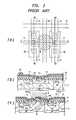
- FIG. 6shows another embodiment of the present invention.
- AI layers 23such as AI wiring leads are arranged in a manner to hold the program part 22 therebetween.
- the thickness of each of the AI layers on both the sidesis made approximately 0.5-2 ⁇ m, and in a case where the programming wiring lead 21 is of AI, the AI layers which are at least two times as thick as the programming AI are provided on both the sides.
- the width of each lead and the interval of the leadsare 2 um, even when a laser beam 5 having a spot diameter of 8 um is used, this laser beam impinges on the adjacent programming wiring lead 25 in only a case where a positional deviation of at least 3 pm has taken place.
- a function element 26can be brought as close to the programming wiring lead 21 as 2 um by causing a part thereof to get under the Al wiring lead 23, and it can be brought as close as 3 um even when a safety width of 1 um is set.
- the laser beam for irradiationis made a rectangular beam based on the projection of a rectangular opening, not a circular beam, the range of the laser irradiation become preciser. Even with the same irradiated size, therefore, the function element can be similarly brought close.
- the present inventionconsists in a semiconductor integrated circuit device in which, in the process of a second layer of Al, a required protective mask is disposed around a part where a wiring lead is to be cut or connected. Therefore, the following functional effects are attained:
Landscapes
- Physics & Mathematics (AREA)
- Engineering & Computer Science (AREA)
- Power Engineering (AREA)
- General Physics & Mathematics (AREA)
- Computer Hardware Design (AREA)
- Microelectronics & Electronic Packaging (AREA)
- Condensed Matter Physics & Semiconductors (AREA)
- Health & Medical Sciences (AREA)
- Electromagnetism (AREA)
- Toxicology (AREA)
- Manufacturing & Machinery (AREA)
- Design And Manufacture Of Integrated Circuits (AREA)
- Internal Circuitry In Semiconductor Integrated Circuit Devices (AREA)
- Semiconductor Memories (AREA)
- Semiconductor Integrated Circuits (AREA)
Description
- The present invention relates to a programmable semiconductor integrated circuit device, and more particularly to a semiconductor integrated circuit device which includes within its circuit wiring, wiring for programming and a laser masking pattern for realizing high productivity without requiring a high precision in laser irradiation for the programming, and a method of producing said device.
- An integrated circuit chip already manufactured can be programmed by disconnecting or short-circuiting parts of the wiring of an integrated circuit. This programming method has heretofore been used for, e.g., the programming of a read- only memory (ROM). In addition, it is recently utilized for the repair of defective cells in a memory device. These prior-art measures have usually employed the following expedients:
- (1) Afuse is blown out by current, thereby to cut a wiring lead.
- (2) Energy is externally applied optically by laser pulses, thereby to cut or connect a wiring lead.
- Figures 1(a) and 1(b) show an example of the prior art. It is a programming method wherein a
wiring lead 3 of polycrystalline Si or AI which is electrically insulated from anSi substrate 1 by an Si02 film 2 is cut by irradiating it with alaser beam 5 through anoverlying passivation film 4. As an example of this method, R. P. Cenker et al. (1979 ISSCC Digest of Technical Papers) have reported that the result of an experiment in which the wiring of decoders in a MOS memory was so altered that the defective cells of the memory connected to the decoders were separated and replaced with non-defective cells connected to dummy decoders. - However, the method in which the elements are disconnected in this manner has the following disadvantages:
- (1) The energy of the laser needs to be high. Moreover, during the cutting, a
material 6 in or around the molten and scattered wiring part damages thepassivation film 4 near by as illustrated in Figure 1 (b), or thelaser beam 5 is prone to damage the substrate near by. Therefore, the layout requires a sufficient margin and results in a large area. - (2) Even with the large area, a satisfactorily high positional accuracy such as ±1 pm for a 3 um pattern is needed for preventing any influence on the surrounding part in case of the laser irradiation of the part to-be-cut. In order to perform processing at high speed in case of mass production, it is required of an apparatus to simultaneously meet the mutually contradictory specifications of the high speed and the high accuracy. Even when the apparatus can be realized, it becomes very expensive. Moreover, from the standpoint of reliability, it is difficult to locate a function element around the part to-be-cut.
- (3) It is sufficient to use only the expedient of cutting. The use of short-circuiting is sometimes advantageous on the occupying area of a chip.
- Figures 2(a) and 2(b) show another example of the prior art. There has been proposed the technique wherein a high-resistivity polycrystalline Si wiring lead (resistanceZ109f)) 3b, which is electrically insulated from an
Si substrate 1 by an Si02 film 2 and which is held between low-resistivity polycrystallineSi wiring lead 3a, is irradiated with alaser 5 through anoverlying passivation film 4 and thus turned into low resistivity and connected as illustrated in Figure 2(b). - However, the method in which the wiring leads are connected in this manner has the following disadvantages:
- (1) The laser irradiation is liable to damage the substrate near by. Therefore the layout requires a sufficient margin and results in a large area.
- (2) Even with large areas, a satisfactorily high positional accuracy is need for suppressing influence on the surrounding part in case of the laser irradiation of the part to-be-connected. In order to perform processing at high speed in case of mass production, an apparatus becomes considerably expensive. Moreover, locating a function element around the part to-be-connected is difficult from the standpoint of reliability.
- (3) It is insufficient to use only the procedure of connection. The combined use with cutting is sometimes advantageous on the occupying area of a chip.
- Figures 3(a) and 3(c) are views illustrating a problem in the case where a function element is arranged around the wiring lead to be cut or connected in the prior art. Figure 3(a) is a plan view, and Figures 3(b) and 3(c) are views of section A-B and section C-D in Figure 3(a), respectively.
Numeral 7 indicates FSG (phosphosilicate glass),numeral 8 Si3N4 (silicon nitride), numeral 11 a first layer of AI wiring, and numeral 12 a second layer of AI wiring. - A Poly-Si (polycrystalline silicon) or
AI wiring lead 3d, which is disposed on anSi substrate 1 with an Si02 film 2 intervening therebetween, is irradiated with alaser 5 from above theSi substrate 1, to cut the Poly-Si orAI wiring lead 3d or to connect the Poly-Si wiring lead 3d. Since, however, an apparatus bears a heavy burden when positioning the laser beam to the wiring part of 2-3 um at high precision and performing processing at high speed, the size of thelaser 5 to irradiate thewiring lead 3d cannot help becoming considerably larger than that of thewiring lead 3d in practical use. Then, incase of this prior-art example,function parts 16 located on both the sides of thewiring lead 3d are partly irradiated with the laser beam, andfunction parts 15 feared to have been thermally influenced arise. Therefore, in order to realize the fast processing at the sacrifice of some precision, the function parts must be spaced from the laser irradiation part to the utmost. This inevitably makes the area of a chip large. - From GB-A-20 47 963 a semiconductor integrated circuit device is known comprising a semiconductor body, an insulating film provided thereon, and a circuit programming wiring layer formed on said insulating film, wherein the programming wiring layer is made of sichrome and is severed by about one tenth of the laser power required to severe A1 conductor lines.
- An object of the present invention is to eliminate the disadvantages of the prior arts described above and to provide a semiconductor integrated circuit device and a method of producing said device which allows an integrated circuit of high packaging density to be programmed at high accuracy, high speed and high reliability.
- To accomplish said object, the invention provides a semiconductor integrated circuit device comprising:
- A semiconductor integrated circuit device comprising a semiconductor body, an insulating film provided on said semiconductor body, and a circuit programming wiring layer formed on said insulating film, characterized in that the semiconductor integrated circuit device further comprises a light shielding protective mask material deposited around said circuit programming wiring layer except a program part thereof or along the longitudinal sides of said circuit programming wiring layer, and an insulating film interposed between said protective mask material and said circuit programming wiring layer.
- To accomplish said object, the invention further provides a method of producing a semiconductor integrated circuit device, wherein a circuit programming wiring layer of polycristalline silicon or of metal is formed on an insulating film which is provided on a semiconductor body and said circuit programming wiring layer is irradiated with a laser beam, characterized in that a light shielding protective mask material is deposited around said circuit programming wiring layer except a program part thereof or along the longitudinal sides of said circuit programming wiring layer, prior to the irradiating step and that an insulating film is interposed between said protective mask material and said circuit programming wiring layer. According to the present invention, in a semiconductor integrated circuit device, at the stage of processing a second layer of AI wiring, a part to be irradiated with a laser had no AI deposited therein and the outer sides thereof are covered with a second layer of AI film, so as to prevent the laser beam from invading impertinent parts, whereby function parts are allowed to be arranged also around the wiring which needs to be subjected to programming such as cutting and connection by the laser, and the programming can be performed at high speed and at high precision without remarkably enhancing the function of a prior-art device. Particularly in case of cutting a first layer of Al, the second layer of AI film is made at least two times as thick as the first layer of AI film by considering the machining threshold value of laser power, lest the second layer of masking AI should be removed down to its bottom even when the first layer of AI wiring has been cut.
- Figures 1(a) and 1(b) are views showing a prior-art example of the cutting of wiring by a laser;
- Figures 2(a) and 2(b) are views showing a prior-art example of the connection of wiring by a laser;
- Figure 3(a) is a plan view illustrating the problem of the laser cutting and connection in the prior arts, Figure 3(b) is a view of section A-B in Figure 3(a), and Figure 3(c) is a view of section C-D in Figure 3(a);
- Figure 4(a) is a plan view showing an embodiment of the semiconductor integrated circuit device of the present invention, Figure 4(b) is a view of section A-B in Figure 4(a), and Figure 4(c) is a view of section C-D in Figure 4(a);
- Figure 5(a) is a plan view showing another embodiment of the semiconductor integrated circuit device of the present invention, Figure 5(b) is a view of section A-B in Figure 5(a), and Figure 5(c) is a view of section C-D in Figure 5(a); and
- Figure 6 is a view showing still another embodiment of the semiconductor integrated circuit device of the present invention.
- Hereunder, the present invention will be concretely described in conjunction with embodiments shown in the drawings.
- Figures 4(a), 4(b) and 4(c) show an embodiment of the present invention. Figure 4(a) is a plan view, Figure 4(b) is a view of section A-B in Figure 4(a), and Figure 4(c) is a view of section C-D in Figure 4(a). A high-resistivity polycrystalline
Si wiring lead 3e is fabricated which is electrically insulated from aSi substrate 1 by an Si02 film 2 and which is held between low-resistivity polycrystalline Si wiring leads 3d of sheet resistance several tens ohms/D. When a second layer of AI film is formed on thewiring lead 3e with aPSG insulating film 7 intervening therebetween, a second layer of A) 17 is provided. The second layer ofAI 17 has a window through which the high-resistivity Poly-Siwiring lead 3e of several gigaohms/D including its perimeter about 1 µm wide can be sufficiently seen, and which covers the perimeter of about 20 microns square. The high-resistivity Poly-Siwiring lead 3e is irradiated through the window of the second layer ofAI film 17 with apulse laser beam 5 by one to several hundred pulses; the pulse laser beam having a beam diameter of 10 pm, a positional accuracy of ± 4 pm, a pulse width of several nano - several tens nanoseconds, a power density on the order of 105―107 W/cm2, and wavelengths of near-infrared to ultraviolet radiation (250 nm-1.2 µm) adapted to permeate through the PSG insulating film. Then, Phosphorus with which the low-resistivity Poly-Si wiring leads 3d on both sides of the high-resistivity Poly-Siwiring lead 3e is doped, and Phosphorus in the overlying PSG layer diffuse into the high-resistivity polycrystalline Si, to lower its sheet resistance into 102―103 ohms/D and to change it from an insulating state into a conductive state circuit-wise. - At this time, the resistance value changes every pulse of the laser irradiation. Therefore, the decrease of the resistance value may be monitored by erecting a whisker on a probing pad (not shown) on a chip, and the irradiation with the laser pulses may be stopped when a predetermined resistance value has been reached. In addition, the machining limit power density of an AI wiring lead approximately 1 µm thick is at least 5 x 10⁸W/cm2. Therefore, the AI wiring lead is not machined, and the part covered with AI is not affected at all even when the laser has impinged thereon.
- In this manner, the perimeter of the high-resistivity Poly-
Si wiring lead 3e to have its resistance lowered by the laser irradiation is covered with the AI mask, whereby the damage of adjacent parts in theSi substrate 1 ascribable to the laser irradiation can be prevented. Accordingly, even when function regions are disposed in the adjacent parts, the high-resistivity polycrystalline silicon is allowed to be processed at a low positional accuracy of the laser irradiation. Therefore, it has become possible to raise the speed of the processing, and to make the integrated circuit still higher in density than in the prior arts. Numeral 8 indicates an Si3N4 film.- Figures 5(a), 5(b) and 5(c) show another embodiment of the present invention. Figure 5(a) is a plan view of the embodiment, Figure 5(b) is a view of section A-B in Figure 5(a), and Figure 5(c) is a view of section C-D in Figure 5(a). There is provided a low-resistivity Poly-
Si wiring lead 3d of several tens ohms/D which is electrically insulated from anSi substrate 1 by an Si02 film 2. When the low-resistivity Poly-Si wiring lead 3d to be cut is overlaid wiht second-layer AI films PSG insulating film 7 therebetween, it is exposed by several microns, and a mask of AI is simultaneously formed so as to cover the perimeter of the position to-be-cut of about 20 µm square with aleft AI mask 19b, which covers the lower part of thewiring lead 3d and the left side of the middle part thereof to be cut and which is separate from a second layer ofAI wiring lead 18, and aright AI mask 19a, which covers the upper part of thewiring lead 3d and the right side of the middle part thereof to be cut and which is separate from the second layer ofAI wiring lead 18. - The
AI mask pulse laser beam 5 by one pulse from above; the pulse laser beam having a beam diameter of about 10 um, a positional accuracy of ±3 µm, a pulse width of several nonoseconds - several tens nanoseconds, and a power density on the order of 107―3 x 10⁸ W/cm2. Then, the Poly-Si wiring lead 3d exposed between AI masks is instantly removed to end the cutting. If necessary, a protective coating is provided after the cutting of the wiring lead. - In this manner, the portion other than the place to be cut is covered with the two
separate AI masks separate AI masks Si wiring lead 3d has been partly short-circuited to theleft AI mask 19b or/and theright AI mask 19a, the short circuit poses no problem because each of the AI masks 19a and 19b does not have any conduction to another part. - As a result, it has become possible to perform the required wiring lead cutting processing at a low positional accuracy of the laser irradiation, and to realize fast production. Moreover, it has become possible to gather function elements also around the part to-be-cut, and to render the packaging density of an integrated circuit higher than in the priors arts.
- Also in a case where the Poly-
Si wiring lead 3d in Figures 5(a), 5(b) and 5(c) is applied to a first layer of AI wiring, similar right and leftAI masks AI wiring lead 3d to be fabricated simultaneously with the first layer ofAI 11 is 1 um thick, the second-layer AI wiring leads 18, 19a and 19b to be fabricated simultaneously with the AI masks 19a and 19b are made at least 2 µm thick so as to have thicknesses not less than double the thickness of the first layer ofAl 11. The place to be cut is irradiated with thepulse laser beam 5 from above the AI masks, the laser beam having as beam diameter of about 10 µm, a positional accuracy of ±3 µm, a pulse width of several nanoseconds - several tens nanoseconds, and a power density on the order of 5 x 10⁸―109 W/cm2. Then, theAI wiring lead 3d is removed instantly. Even when the peripheral parts of the AI masks have been somewhat damaged, they do not penetrate through the underlying part to affect function parts within theSi substrate 1. In addition, even when the cut part of the AI wiring lead has short-circuited to the right or leftAI mask - In this way, it has become possible to perform the required AI wiring cutting processing at a comparatively low accuracy, and to realize fast production. Moreover, it has become possible to gather function elements around the part to-be-cut, and to render the packaging density of an integrated circuit higher than in the prior arts.
- Figure 6 shows another embodiment of the present invention. Near a
program part 22 of aprogramming wiring lead 21, AI layers 23 such as AI wiring leads are arranged in a manner to hold theprogram part 22 therebetween. In a case where theprogramming wiring lead 21 is of Poly-Si, the thickness of each of the AI layers on both the sides is made approximately 0.5-2 µm, and in a case where theprogramming wiring lead 21 is of AI, the AI layers which are at least two times as thick as the programming AI are provided on both the sides. Supposing herein that the width of each lead and the interval of the leads are 2 um, even when alaser beam 5 having a spot diameter of 8 um is used, this laser beam impinges on the adjacentprogramming wiring lead 25 in only a case where a positional deviation of at least 3 pm has taken place. In addition, when the width of each of the AI wiring leads 23 on both the sides is made at least 4 pm, afunction element 26 can be brought as close to theprogramming wiring lead 21 as 2 um by causing a part thereof to get under theAl wiring lead 23, and it can be brought as close as 3 um even when a safety width of 1 um is set. - When the laser beam for irradiation is made a rectangular beam based on the projection of a rectangular opening, not a circular beam, the range of the laser irradiation become preciser. Even with the same irradiated size, therefore, the function element can be similarly brought close.
- As set forth above, the present invention consists in a semiconductor integrated circuit device in which, in the process of a second layer of Al, a required protective mask is disposed around a part where a wiring lead is to be cut or connected. Therefore, the following functional effects are attained:
- (1) An irradiating laser beam for the cutting or connection can be used in a large size which is not restricted by a pattern size.
- (2) The irradiating positional accuracy of the beam may be within ±3 pm for pattern sizes of at most 5 µm, and a conspicuously high accuracy of ±1 µm as in the prior art is not required. Therefore, a table speed can be raised, and the speed of the cutting or connecting processing can be sharply raised.
- (3) Function elements are allowed to be arranged around a wiring lead to-be-cut or -connected, and the packaging density of an integrated circuit can be made higher than in the prior art.
Claims (10)
Applications Claiming Priority (2)
| Application Number | Priority Date | Filing Date | Title |
|---|---|---|---|
| JP153695/81 | 1981-09-30 | ||
| JP56153695AJPS5856355A (en) | 1981-09-30 | 1981-09-30 | Semiconductor integrated circuit device |
Publications (3)
| Publication Number | Publication Date |
|---|---|
| EP0075926A2 EP0075926A2 (en) | 1983-04-06 |
| EP0075926A3 EP0075926A3 (en) | 1985-05-08 |
| EP0075926B1true EP0075926B1 (en) | 1987-12-16 |
Family
ID=15568105
Family Applications (1)
| Application Number | Title | Priority Date | Filing Date |
|---|---|---|---|
| EP82108968AExpiredEP0075926B1 (en) | 1981-09-30 | 1982-09-28 | Semiconductor integrated circuit device |
Country Status (5)
| Country | Link |
|---|---|
| US (1) | US4581628A (en) |
| EP (1) | EP0075926B1 (en) |
| JP (1) | JPS5856355A (en) |
| KR (1) | KR900002087B1 (en) |
| DE (1) | DE3277855D1 (en) |
Families Citing this family (36)
| Publication number | Priority date | Publication date | Assignee | Title |
|---|---|---|---|---|
| JPS59957A (en)* | 1982-06-25 | 1984-01-06 | Fujitsu Ltd | semiconductor equipment |
| JPS59201441A (en)* | 1983-04-30 | 1984-11-15 | Toshiba Corp | Fuse cutting method utilizing converged ion beam |
| CA1186070A (en)* | 1983-06-17 | 1985-04-23 | Iain D. Calder | Laser activated polysilicon connections for redundancy |
| US4924287A (en)* | 1985-01-20 | 1990-05-08 | Avner Pdahtzur | Personalizable CMOS gate array device and technique |
| JPH0789567B2 (en)* | 1985-02-25 | 1995-09-27 | 株式会社日立製作所 | Semiconductor device |
| JPH0719842B2 (en)* | 1985-05-23 | 1995-03-06 | 三菱電機株式会社 | Redundant circuit of semiconductor device |
| JPH0821623B2 (en)* | 1985-09-20 | 1996-03-04 | 株式会社日立製作所 | Laser processing method |
| US4681778A (en)* | 1985-11-14 | 1987-07-21 | Optical Materials, Inc. | Method and apparatus for making electrical connections utilizing a dielectric-like metal film |
| US5329152A (en)* | 1986-11-26 | 1994-07-12 | Quick Technologies Ltd. | Ablative etch resistant coating for laser personalization of integrated circuits |
| IL82113A (en)* | 1987-04-05 | 1992-08-18 | Zvi Orbach | Fabrication of customized integrated circuits |
| US5223735A (en)* | 1988-09-30 | 1993-06-29 | Mitsubishi Denki Kabushiki Kaisha | Semiconductor integrated circuit device in which circuit functions can be remedied or changed and the method for producing the same |
| US4974048A (en)* | 1989-03-10 | 1990-11-27 | The Boeing Company | Integrated circuit having reroutable conductive paths |
| JP2816394B2 (en)* | 1989-10-24 | 1998-10-27 | セイコークロック株式会社 | Semiconductor device |
| DE69333881T2 (en) | 1992-07-31 | 2006-07-13 | Hughes Electronics Corp., El Segundo | Integrated circuit safety system and method with implanted connections |
| TW278229B (en)* | 1994-12-29 | 1996-06-11 | Siemens Ag | Fuse structure for an integrated circuit device and method for manufacturing a fuse structure |
| JPH0935917A (en)* | 1995-07-17 | 1997-02-07 | Mitsubishi Electric Corp | Trimming device and method for hybrid integrated circuit |
| US5783846A (en)* | 1995-09-22 | 1998-07-21 | Hughes Electronics Corporation | Digital circuit with transistor geometry and channel stops providing camouflage against reverse engineering |
| US5986319A (en)* | 1997-03-19 | 1999-11-16 | Clear Logic, Inc. | Laser fuse and antifuse structures formed over the active circuitry of an integrated circuit |
| JP3037191B2 (en)* | 1997-04-22 | 2000-04-24 | 日本電気アイシーマイコンシステム株式会社 | Semiconductor device |
| US5973375A (en)* | 1997-06-06 | 1999-10-26 | Hughes Electronics Corporation | Camouflaged circuit structure with step implants |
| JP4255142B2 (en)* | 1998-02-05 | 2009-04-15 | 株式会社ルネサステクノロジ | Semiconductor device |
| US6396368B1 (en) | 1999-11-10 | 2002-05-28 | Hrl Laboratories, Llc | CMOS-compatible MEM switches and method of making |
| US7217977B2 (en)* | 2004-04-19 | 2007-05-15 | Hrl Laboratories, Llc | Covert transformation of transistor properties as a circuit protection method |
| US6815816B1 (en) | 2000-10-25 | 2004-11-09 | Hrl Laboratories, Llc | Implanted hidden interconnections in a semiconductor device for preventing reverse engineering |
| US6791191B2 (en) | 2001-01-24 | 2004-09-14 | Hrl Laboratories, Llc | Integrated circuits protected against reverse engineering and method for fabricating the same using vias without metal terminations |
| US7294935B2 (en)* | 2001-01-24 | 2007-11-13 | Hrl Laboratories, Llc | Integrated circuits protected against reverse engineering and method for fabricating the same using an apparent metal contact line terminating on field oxide |
| US6740942B2 (en)* | 2001-06-15 | 2004-05-25 | Hrl Laboratories, Llc. | Permanently on transistor implemented using a double polysilicon layer CMOS process with buried contact |
| US6774413B2 (en) | 2001-06-15 | 2004-08-10 | Hrl Laboratories, Llc | Integrated circuit structure with programmable connector/isolator |
| US6897535B2 (en)* | 2002-05-14 | 2005-05-24 | Hrl Laboratories, Llc | Integrated circuit with reverse engineering protection |
| US6700161B2 (en)* | 2002-05-16 | 2004-03-02 | International Business Machines Corporation | Variable resistor structure and method for forming and programming a variable resistor for electronic circuits |
| US7049667B2 (en) | 2002-09-27 | 2006-05-23 | Hrl Laboratories, Llc | Conductive channel pseudo block process and circuit to inhibit reverse engineering |
| US6979606B2 (en)* | 2002-11-22 | 2005-12-27 | Hrl Laboratories, Llc | Use of silicon block process step to camouflage a false transistor |
| WO2004055868A2 (en)* | 2002-12-13 | 2004-07-01 | Hrl Laboratories, Llc | Integrated circuit modification using well implants |
| US7242063B1 (en) | 2004-06-29 | 2007-07-10 | Hrl Laboratories, Llc | Symmetric non-intrusive and covert technique to render a transistor permanently non-operable |
| US7675796B2 (en)* | 2005-12-27 | 2010-03-09 | Semiconductor Energy Laboratory Co., Ltd. | Semiconductor device |
| US8168487B2 (en)* | 2006-09-28 | 2012-05-01 | Hrl Laboratories, Llc | Programmable connection and isolation of active regions in an integrated circuit using ambiguous features to confuse a reverse engineer |
Family Cites Families (11)
| Publication number | Priority date | Publication date | Assignee | Title |
|---|---|---|---|---|
| US3584183A (en)* | 1968-10-03 | 1971-06-08 | North American Rockwell | Laser encoding of diode arrays |
| JPS5130437B1 (en)* | 1970-03-25 | 1976-09-01 | ||
| BE794202A (en)* | 1972-01-19 | 1973-05-16 | Intel Corp | FUSE LINK FOR INTEGRATED CIRCUIT ON SEMICONDUCTOR SUBSTRATE FOR MEMORIES |
| JPS5910587B2 (en)* | 1977-08-10 | 1984-03-09 | 株式会社日立製作所 | Semiconductor device protection device |
| US4272775A (en)* | 1978-07-03 | 1981-06-09 | National Semiconductor Corporation | Laser trim protection process and structure |
| US4228451A (en)* | 1978-07-21 | 1980-10-14 | Monolithic Memories, Inc. | High resistivity semiconductor resistor device |
| JPS582439B2 (en)* | 1978-11-27 | 1983-01-17 | 富士通株式会社 | bootstrap circuit |
| US4238839A (en)* | 1979-04-19 | 1980-12-09 | National Semiconductor Corporation | Laser programmable read only memory |
| DE3036869C2 (en)* | 1979-10-01 | 1985-09-05 | Hitachi, Ltd., Tokio/Tokyo | Semiconductor integrated circuit and circuit activation method |
| JPS5775442A (en)* | 1980-10-29 | 1982-05-12 | Toshiba Corp | Semiconductor device |
| JPS58170A (en)* | 1981-06-24 | 1983-01-05 | Mitsubishi Electric Corp | semiconductor equipment |
- 1981
- 1981-09-30JPJP56153695Apatent/JPS5856355A/enactiveGranted
- 1982
- 1982-09-27USUS06/424,370patent/US4581628A/ennot_activeExpired - Fee Related
- 1982-09-28EPEP82108968Apatent/EP0075926B1/ennot_activeExpired
- 1982-09-28DEDE8282108968Tpatent/DE3277855D1/ennot_activeExpired
- 1982-09-29KRKR8204389Apatent/KR900002087B1/ennot_activeExpired
Also Published As
| Publication number | Publication date |
|---|---|
| JPS5856355A (en) | 1983-04-04 |
| JPH0312464B2 (en) | 1991-02-20 |
| US4581628A (en) | 1986-04-08 |
| EP0075926A2 (en) | 1983-04-06 |
| DE3277855D1 (en) | 1988-01-28 |
| KR900002087B1 (en) | 1990-03-31 |
| EP0075926A3 (en) | 1985-05-08 |
| KR840001777A (en) | 1984-05-16 |
Similar Documents
| Publication | Publication Date | Title |
|---|---|---|
| EP0075926B1 (en) | Semiconductor integrated circuit device | |
| US4751197A (en) | Make-link programming of semiconductor devices using laser enhanced thermal breakdown of insulator | |
| US4665295A (en) | Laser make-link programming of semiconductor devices | |
| US4912066A (en) | Make-link programming of semiconductor devices using laser-enhanced thermal breakdown of insulator | |
| EP0162145B1 (en) | Method of melting a fuse using a laser beam | |
| US4628590A (en) | Method of manufacture of a semiconductor device | |
| US8115274B2 (en) | Fuse structure and method for manufacturing same | |
| KR20010007252A (en) | Semiconductor device with repair fuses and laser trimming method used therefor | |
| EP0720230B1 (en) | Fuse structure for an integrated circuit device | |
| KR100276746B1 (en) | Semiconductor device with laser make-link programmable fuse | |
| EP0324407B1 (en) | Trimming process by a laser beam | |
| US3846905A (en) | Assembly method for semiconductor chips | |
| KR950001753B1 (en) | Semiconductor device and manufacturing method | |
| JPS61194740A (en) | Semiconductor device | |
| JPS6193643A (en) | Semiconductor programmable with laser beam and manufacture thereof | |
| EP0602271B1 (en) | Testing and repairing process for memory chips on a wafer, each chip having a redundancy circuit | |
| JP2508293B2 (en) | Semiconductor device and manufacturing method thereof | |
| EP0887858A2 (en) | Protection layer for laser blown fuses in semiconductor devices | |
| KR100206916B1 (en) | Pad protecting method of semiconductor chip against di water | |
| JPH08274178A (en) | Method for manufacturing semiconductor device | |
| KR100301806B1 (en) | Semiconductor device | |
| KR101033987B1 (en) | Repair method of semiconductor device | |
| CN114864547A (en) | Semiconductor structure and method for manufacturing semiconductor structure | |
| JPS61176135A (en) | Semiconductor device | |
| HK1003959A (en) | Fuse structure for an integrated circuit device |
Legal Events
| Date | Code | Title | Description |
|---|---|---|---|
| PUAI | Public reference made under article 153(3) epc to a published international application that has entered the european phase | Free format text:ORIGINAL CODE: 0009012 | |
| AK | Designated contracting states | Designated state(s):DE FR GB IT | |
| PUAL | Search report despatched | Free format text:ORIGINAL CODE: 0009013 | |
| AK | Designated contracting states | Designated state(s):DE FR GB IT | |
| 17P | Request for examination filed | Effective date:19850513 | |
| 17Q | First examination report despatched | Effective date:19860827 | |
| GRAA | (expected) grant | Free format text:ORIGINAL CODE: 0009210 | |
| AK | Designated contracting states | Kind code of ref document:B1 Designated state(s):DE FR GB IT | |
| REF | Corresponds to: | Ref document number:3277855 Country of ref document:DE Date of ref document:19880128 | |
| ET | Fr: translation filed | ||
| ITF | It: translation for a ep patent filed | ||
| PLBE | No opposition filed within time limit | Free format text:ORIGINAL CODE: 0009261 | |
| STAA | Information on the status of an ep patent application or granted ep patent | Free format text:STATUS: NO OPPOSITION FILED WITHIN TIME LIMIT | |
| 26N | No opposition filed | ||
| ITTA | It: last paid annual fee | ||
| PGFP | Annual fee paid to national office [announced via postgrant information from national office to epo] | Ref country code:FR Payment date:19980916 Year of fee payment:17 | |
| PGFP | Annual fee paid to national office [announced via postgrant information from national office to epo] | Ref country code:GB Payment date:19980918 Year of fee payment:17 | |
| PGFP | Annual fee paid to national office [announced via postgrant information from national office to epo] | Ref country code:DE Payment date:19981127 Year of fee payment:17 | |
| PG25 | Lapsed in a contracting state [announced via postgrant information from national office to epo] | Ref country code:GB Free format text:LAPSE BECAUSE OF NON-PAYMENT OF DUE FEES Effective date:19990928 | |
| GBPC | Gb: european patent ceased through non-payment of renewal fee | Effective date:19990928 | |
| PG25 | Lapsed in a contracting state [announced via postgrant information from national office to epo] | Ref country code:FR Free format text:LAPSE BECAUSE OF NON-PAYMENT OF DUE FEES Effective date:20000531 | |
| PG25 | Lapsed in a contracting state [announced via postgrant information from national office to epo] | Ref country code:DE Free format text:LAPSE BECAUSE OF NON-PAYMENT OF DUE FEES Effective date:20000701 | |
| REG | Reference to a national code | Ref country code:FR Ref legal event code:ST |