EP0050583B1 - Alternating voltage to direct current converter and oscillator circuit comprising said converter - Google Patents
Alternating voltage to direct current converter and oscillator circuit comprising said converterDownload PDFInfo
- Publication number
- EP0050583B1 EP0050583B1EP81810349AEP81810349AEP0050583B1EP 0050583 B1EP0050583 B1EP 0050583B1EP 81810349 AEP81810349 AEP 81810349AEP 81810349 AEP81810349 AEP 81810349AEP 0050583 B1EP0050583 B1EP 0050583B1
- Authority
- EP
- European Patent Office
- Prior art keywords
- transistor
- converter
- current
- terminal
- gate
- Prior art date
- Legal status (The legal status is an assumption and is not a legal conclusion. Google has not performed a legal analysis and makes no representation as to the accuracy of the status listed.)
- Expired
Links
- 239000003990capacitorSubstances0.000claimsdescription11
- 238000012886linear functionMethods0.000claimsdescription5
- 230000003247decreasing effectEffects0.000claimsdescription4
- 230000010355oscillationEffects0.000abstractdescription6
- 230000001105regulatory effectEffects0.000abstract1
- 230000000630rising effectEffects0.000abstract1
- 238000012423maintenanceMethods0.000description9
- 230000007423decreaseEffects0.000description6
- 238000010586diagramMethods0.000description5
- 229910021420polycrystalline siliconInorganic materials0.000description2
- 239000010453quartzSubstances0.000description2
- VYPSYNLAJGMNEJ-UHFFFAOYSA-Nsilicon dioxideInorganic materialsO=[Si]=OVYPSYNLAJGMNEJ-UHFFFAOYSA-N0.000description2
- 230000000295complement effectEffects0.000description1
- 230000001419dependent effectEffects0.000description1
- 230000000694effectsEffects0.000description1
- 235000021183entréeNutrition0.000description1
- 230000001747exhibiting effectEffects0.000description1
- 238000004519manufacturing processMethods0.000description1
Images

Classifications
- G—PHYSICS
- G04—HOROLOGY
- G04G—ELECTRONIC TIME-PIECES
- G04G19/00—Electric power supply circuits specially adapted for use in electronic time-pieces
- G04G19/02—Conversion or regulation of current or voltage
- G04G19/06—Regulation
- H—ELECTRICITY
- H03—ELECTRONIC CIRCUITRY
- H03L—AUTOMATIC CONTROL, STARTING, SYNCHRONISATION OR STABILISATION OF GENERATORS OF ELECTRONIC OSCILLATIONS OR PULSES
- H03L5/00—Automatic control of voltage, current, or power
Definitions
- the present inventionrelates to a converter of an alternating voltage into a direct current, of the type comprising supply terminals, an input terminal and an output terminal.
- the inventionalso relates to an oscillator circuit applying this converter.
- the inventionrelates, more particularly, to oscillators with very low current consumption which are used in watches.
- a regulator circuitmaintains the amplitude of the oscillation signal at a low value, in order to minimize the current consumption of this oscillator.
- the amplitude of the oscillation signalmust however be sufficient to allow the use of this signal in the following circuits such as: amplifiers, frequency divider, etc.
- This known circuitwhich is represented in FIG. 1, comprises a maintenance circuit 1 for the vibrations of a quartz resonator 2, and an amplitude regulator 3.
- the maintenance circuit 1comprises a polarized amplifier MOS transistor 4 by a resistor 5; the drain-source path of transistor 4 is connected in series with that of another MOS transistor 6, between the + V and - V terminals of a supply voltage source.
- the transistor 6plays the role of an adjustable current source supplying the amplifier transistor 4 of the maintenance circuit 1.
- the control terminal of the current source 6, which is the gate 6a of this transistor 6,receives a signal from control provided by the regulator circuit 3 which itself receives on its input 3a via a decoupling capacitor 7, an oscillation signal from the oscillator, signal present on an input terminal 8 of the oscillator circuit.
- the regulator circuit 3comprises four MOS transistors 9 to 12 connected in pairs in mirrors and forming a closed loop whose gain is limited by a resistance constituted by a fifth transistor 13.
- the regulator circuit 3 and the transistor 6together constitute a converter d '' an alternating input voltage into a direct current.
- This known converterby design, requires a bias network of the transistors comprising resistors 14, 15 of very high value constituted by diodes produced in polycrystalline silicon. As a result, this known circuit can only be produced in a technology in which the gates of the MOS transistors are produced in highly doped polycrystalline silicon.
- the object of the present inventionis in particular to propose a converter from an alternating voltage to a direct current, which can be produced in any technology.
- the converter according to the preamble of claim 1comprises a first elementary converter supplying, in response to an input alternating voltage, a pulsed direct current i 1 whose average value is a function strongly increasing the amplitude A of said alternating voltage, and a second elementary converter supplying, in response to the current i 1 , the current i 3 whose value is a strongly decreasing function of i 1 , a function such that we have, in a certain range of values of A, substantially: where Ci is a constant parameter and A M a particular value of A located in said range of values.
- This value of i 3is therefore a linearly decreasing function at A.
- the first elementary convertercomprises a first MOS transistor, the gate of which is connected to the input terminal of the converter by means of a decoupling capacitor, and means for biasing this first transistor.
- These biasing meansadvantageously comprise a circuit responding to the input alternating voltage for applying between the gate and the source of this MOS transistor a biasing voltage whose mean value is a substantially linear function of the amplitude A of the alternating voltage .
- This circuit responding to alternating voltage inputcomprises advantageously: a second MOS transistor one of the channel terminals of which is connected to the gate of the first transistor, and a bias circuit of this second transistor, arranged to apply between the second channel terminal and the gate of the second transistor, a constant voltage chosen so that the impedance of this second transistor is high.
- the second elementary convertercomprises a third, a fourth and a fifth MOS transistor, means responding to the current i 2 flowing in the fourth transistor to apply between the gate and the source of the third transistor a control voltage which is a linear function of the average value of said current flowing in the fourth transistor, this control voltage being such that the third transistor always operates at low inversion, the fourth and fifth transistors having their gates connected together and their sources connected to the same supply terminal, the drain of the fifth transistor being connected to the output terminal of the converter, and means responding to the current i 1 supplied by the first converter to apply a gate-source bias voltage to the fourth transistor such that the average value of the current in the third transistor is equal to the v average value of current i i .
- the drains of the first and third transistorsare connected together as well as to the gate of the fourth transistor and to an armature of a capacitor (forming part of the means responding to the current i 1 ) the other armature of which is connected to a first supply terminal, the gate of the third transistor receives a constant potential while the source of said third transistor is connected to the drain of the fourth transistor and to a terminal of a resistor (forming part of the means responding to the current i 2 ) the other terminal of which is connected to the second supply terminal, the source of the fourth transistor being connected to the said first supply terminal, the components of the converter being dimensioned so that the current passing through the fourth transistor is generally large vis-à-vis that which flows in the third transistor.
- This converteris advantageously used in an oscillator circuit comprising: a first and a second supply terminal, a maintenance circuit comprising an input terminal, an output terminal, a first and a second terminal for the connection of a resonator, at least one active amplifier element and means for biasing this active element, this oscillation circuit being characterized in that it further comprises a converter as described above comprising an input terminal and an output terminal, the input terminal of said converter being connected to the input terminal or to the output terminal of the maintenance circuit, the output terminal of said converter being connected to the current path of the active element .
- the circuit of FIG. 2comprises a first + V and a second M supply terminal, a maintenance circuit 1 comprising terminals 16 and 17 for the connection of a resonator 2, a input terminal 8 and an output terminal 18.
- the maintenance circuit shown in FIG. 2comprises two complementary MOS transistors connected as an inverter 19 and 20. This type of inverter circuit being well known per se, it will not be further described here.
- a current source produced in the form of an MOS transistor 6is connected in series with the drain-source paths of the active elements 19, 20.
- the control terminal (gate 6a) of the current source 6receives a control signal supplied by a regulator circuit forming with the current source 6 a converter 300 of an alternating input voltage SP into a direct current i 3 , converter whose structure differs fundamentally from that of converter shown in Figure 1.
- the converter 300comprises three parts: a voltage-current converter part 21, a current-current converter part 22, and a bias circuit 23.
- Part 21includes a MOS transistor 24, one channel terminal 24a of which receives, via a capacitor 7, the oscillation signal SP or control signal present on the input terminal 8 of the maintenance circuit 1.
- the other terminal channel 24breceives a constant potential U 1 supplied by the bias circuit 23, and the gate 24c of the transistor 24 receives a constant potential U 2 supplied by the bias circuit 23.
- the voltage U 1is supplied by a channel MOS transistor P 25 whose gate is connected to the drain and whose source is connected to the + V terminal.
- the potential U 2is, in absolute value, greater than the potential U 1 by about a threshold voltage value.
- This potential U 2is supplied by a second P-channel MOS transistor 26, the gate of which is connected to the drain, and the source of which is connected to the drain of transistor 25.
- the signal SPis zero and the P-channel transistor 24 is controlled by a gate-source voltage which is of the order of magnitude of that of a threshold voltage, so that this transistor 24 will behave like a high value resistance traversed by a very low current.
- the signal SPis different from zero and the operation of the transistor 24 will be different according to the sign of the signal SP which is applied to it on its channel terminal 24a.
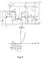
- FIG. 3we have plotted on the abscissa the potential difference between the potential U A of terminal 24a and the potential U B of terminal 24b of transistor 24.
- the current I flowing in the drain-source path of transistor 24On the ordinate of the diagram of FIG. 3, we have represented the current I flowing in the drain-source path of transistor 24.
- the operation of the transistor 24is as follows: during the negative half-waves of the signal SP, the terminal 24a is negative with respect to the terminal 24b, so that the transistor 24 is traversed by a low current substantially independent of the value of the potential of the terminal 24a. During the positive half-waves of the signal SP, the terminal 24a becomes positive with respect to the terminal 24b, so that the current i flowing through the transistor 24 increases exponentially as a function of the potential of the terminal 24a. However due to the presence of the capacitor 7, the charge fidt during a negative alternation must be equal to the charge during a positive alternation of the signal SP.
- the terminal 24abecomes positive with respect to the terminal 24b only for a very short time coinciding with the positive peaks of the signal SP. During this time, the potential of terminal 24a remains close to that of terminal 24b, that is to say that the potential of terminal 24a remains close to the value U 1 .
- the voltage signal P 1 present on terminal 24a and represented in FIG. 3has an average value P 1 , the value of which is a substantially linear function of the amplitude A of the signal SP.
- the signal P 1is applied to the gate 27a of a P channel transistor 27 whose source 27b is connected to the supply terminal + V, and whose drain 27c is connected to the input terminal 22a of the converter circuit current-current 22.
- the transistor 27delivers to the converter 22 a pulsed direct current i 1 whose average value i 1 is strongly dependent on the amplitude A of the alternating input signal SP.
- the current i 1which it supplies increases as an exponential function with the absolute value of the voltage signal P 1 applied to its gate 27a.
- the increase in current i 1 during the negative alternation of the signal SPgreatly exceeds the reduction in current i 1 during the positive alternation of this signal SP.
- the average voltage P 1also decreases with the amplitude A of the signal SP, the current i 1 increases considerably as a function of this amplitude A.
- the role of the current-current converteris to supply, in response to the current i 1 supplied by the transistor 27, a current i 3 whose value is a decreasing function of i 1 .
- i 3must become zero for a given value A M of the amplitude of the input signal SP and it must, in a wide range close to zero, decrease roughly linearly as a function of the amplitude A of the signal SP input.
- the amplitude regulator 300is used in a looped system which need not be necessarily stable. In this set, it is desirable that the transfer function of the regulator circuit is well defined and remains reproducible despite the influence of the parameters of the circuit's manufacturing process.
- the current-to-current converter 22includes an N-channel MOS transistor 28; the gate 28a of the transistor 28 receives a constant potential U 3 supplied by an N-channel MOS transistor 29 whose gate is connected to the drain and whose source is connected to the supply terminal M.
- the drain 28b of the transistor 28is connected at the input 22a of the converter 22.
- the transistor 28is therefore controlled by a voltage U R applied to its source 28c.
- the transistor 28works in low inversion, there is an exponential dependence between the current flowing in this transistor 28 and the control voltage U R of this transistor.
- the voltage U Ris produced by the voltage drop due to the circulation of a current i 2 in a resistor 30, the current i 2 being supplied by a P-channel MOS transistor 31 whose drain-source path is connected in series with resistor 30 between the supply terminals + V and M.
- the gate 31a of the transistor 31is connected to the input 22a of the converter 22, as well as to an armature of a capacitor 32 whose other armature is connected to the supply terminal + V.
- the role of the capacitor 32is maintain roughly constant for a period of the input signal SP, the voltage of the gate 31a and therefore the voltage of the drain 28b of the transistor 28.
- the components of the circuit 300are dimensioned so that the current flowing in the transistor 28 can generally be considered negligible compared to the current flowing in the transistor 31.
- the transistor 6can be dimensioned with respect to the transistor 31 so as to supply a current i 3 suitable for controlling the maintenance circuit 1.
- the transistors 25, 26 and 29 supplying the constant voltages U 1 , U 2 and U 3form part of the bias circuit 23 which further comprises: a current source 33 connected in series, between the supply terminals + V and M , with the drain-source path of transistor 29, and a fourth N-channel transistor 34, the drain-source path of which is connected between the supply terminal M and the drain of transistor 26.
- the sources 6b and 31 of the transistors 6 and 31are connected to the supply terminal + V while the drain 6c of the transistor 6 is connected to the output terminal S of the converter 300.
- the transistor 6is P-channel.
- the starting current i 30 supplied by the transistor 6can be adjusted to the desired value.
- the value 10 of the current supplied by the current source 33 of the bias circuit 23does not play any role as long as the transistors 28 and 29 and 34 work in low inversion.
- This current 1 0therefore does not need to be stabilized, for example vis-à-vis fluctuations in the supply voltage provided by the + V, M.
- the threshold voltages of the transistorsdo not intervene .
- the only factor involved in the transfer function of the converter 300is the transconductance of the transistors 24 and 27; this transconductivity is however a characteristic exhibiting good reproducibility which is in any case sufficient for the application envisaged here.
Landscapes
- Engineering & Computer Science (AREA)
- Power Engineering (AREA)
- Physics & Mathematics (AREA)
- General Physics & Mathematics (AREA)
- Amplifiers (AREA)
- Dc-Dc Converters (AREA)
- Oscillators With Electromechanical Resonators (AREA)
- Rectifiers (AREA)
- Inductance-Capacitance Distribution Constants And Capacitance-Resistance Oscillators (AREA)
- Measurement Of Current Or Voltage (AREA)
- Details Of Television Scanning (AREA)
Abstract
Description
Translated fromFrenchLa présente invention concerne un convertisseur d'une tension alternative en un courant continu, du type comportant des bornes d'alimentation, une borne d'entrée et une borne de sortie.The present invention relates to a converter of an alternating voltage into a direct current, of the type comprising supply terminals, an input terminal and an output terminal.
L'invention concerne aussi un circuit d'oscillateur faisant application de ce convertisseur.The invention also relates to an oscillator circuit applying this converter.
L'invention concerne, plus particulièrement, les oscillateurs à très faible consommation de courant qui sont utilisés dans les montres.The invention relates, more particularly, to oscillators with very low current consumption which are used in watches.
Dans de tels oscillateurs, un circuit régulateur maintient l'amplitude du signal d'oscillation à une valeur faible, afin de minimiser la consommation de courant de cet oscillateur. L'amplitude du signal d'oscillation doit toutefois être suffisante pour permettre l'utilisation de ce signal dans des circuits suivants tels que : amplificateurs, diviseur de fréquence, etc.In such oscillators, a regulator circuit maintains the amplitude of the oscillation signal at a low value, in order to minimize the current consumption of this oscillator. The amplitude of the oscillation signal must however be sufficient to allow the use of this signal in the following circuits such as: amplifiers, frequency divider, etc.
Dans l'article de E. A. VITTOZ « Quartz oscilla- tors for watches publié dans les actes du dixième Congrès International de Chronométrie, Genève, Septembre 1979, volume 3, pages 131-140, on décrit un circuit d'oscillateur du type susmentionné. Ce circuit connu, qui est représenté sur la figure 1, comprend un circuit d'entretien 1 des vibrations d'un résonateur à quartz 2, et un régulateur d'amplitude 3. Le circuit d'entretien 1 comporte un transistor MOS amplificateur 4 polarisé par une résistance 5 ; le trajet drain-source du transistor 4 est branché en série avec celui d'un autre transistor MOS 6, entre les bornes + V et - V d'une source de tension d'alimentation. Le transistor 6 joue le rôle d'une source de courant réglable alimentant le transistor amplificateur 4 du circuit d'entretien 1. La borne de commande de la source de courant 6, qui est la grille 6a de ce transistor 6, reçoit un signal de commande fourni par le circuit régulateur 3 qui reçoit lui-même sur son entrée 3a via un condensateur de découplage 7, un signal d'oscillation de l'oscillateur, signal présent sur une borne d'entrée 8 du circuit d'oscillateur. Le circuit régulateur 3 comprend quatre transistors MOS 9 à 12 connectés deux à deux en miroirs et formant une boucle fermée dont le gain est limité par une résistance constituée par un cinquième transistor 13. Le circuit régulateur 3 et le transistor 6 constituent ensemble un convertisseur d'une tension alternative d'entrée en un courant continu. Ce convertisseur connu, de par sa conception, nécessite un réseau de polarisation des transistors comportant des résistances 14, 15 de très haute valeur constituées par des diodes réalisées dans le silicium polycristallin. Il en résulte que ce circuit connu ne peut être réalisé que dans une technologie dans laquelle les grilles des transistors MOS sont réalisées en silicium polycristallin fortement dopé.In the article by E. A. VITTOZ “Oscillating quartz for watches published in the proceedings of the tenth International Chronometry Congress, Geneva, September 1979,
C'est pourquoi la présente invention a notamment pour objet de proposer un convertisseur d'une tension alternative en un courant continu, pouvant être réalisé dans n'importe quelle technologie.This is why the object of the present invention is in particular to propose a converter from an alternating voltage to a direct current, which can be produced in any technology.
Ce but est atteint conformément à l'invention du fait que le convertisseur selon le préambule de la revendication 1 comprend un premier convertisseur élémentaire fournissant en réponse à une tension alternative d'entrée, un courant continu pulsé i1 dont la valeur moyenne est une fonction fortement croissante de l'amplitude A de ladite tension alternative, et un second convertisseur élémentaire fournissant, en réponse au courant i1, le courant i3 dont la valeur est une fonction fortement décroissante de i1, fonction telle que l'on ait, dans un certain domaine de valeurs de A, sensiblement :
Avantageusement, le premier convertisseur élémentaire est agencé pour fournir un courant i1 tel que i1 = i10 exp A/Uc où i10 et Uc sont des paramètres constants,Advantageously, the first elementary converter is arranged to supply a current i1 such that i1 = i10 exp A / Uc where i10 and Uc are constant parameters,
et le second convertisseur élémentaire est agencé pour fournir un courant i3 tel que i3 = i30 - C1 In (il) où i3o est une constante.and the second elementary converter is arranged to supply a current i3 such that i3 = i30 - C1 In (il) where i3o is a constant.
Il en résulte que l'on a :
Cette valeur de i3 est donc bien une fonction décroissant linéairement en A.This value of i3 is therefore a linearly decreasing function at A.
Les caractéristiques respectivement exponentielles et logarithmiques de ces convertisseurs élémentaires peuvent chacune être obtenues en première approximation au moyen de transistors MOS travaillant sensiblement en faible inversion, sans nécessiter l'utilisation de résistances de haute valeur. Il est en effet bien connu qu'un transistor MOS auquel on applique une tension de polarisation grille-source dont la valeur est inférieure à celle du seuil théorique, ce transistor fournit sur son trajet drain-source un courant dont la valeur est une fonction exponentielle de celle de ladite tension de polarisation.The respectively exponential and logarithmic characteristics of these elementary converters can each be obtained as a first approximation by means of MOS transistors working substantially in low inversion, without requiring the use of high value resistors. It is indeed well known that a MOS transistor to which a gate-source bias voltage is applied whose value is less than that of the theoretical threshold, this transistor provides a current on its drain-source path whose value is an exponential function that of said bias voltage.
Selon un mode de réalisation particulier, le premier convertisseur élémentaire comprend un premier transistor MOS dont la grille est connectée à la borne d'entrée du convertisseur par l'intermédiaire d'un condensateur de découplage, et des moyens de polarisation de ce premier transistor. Ces moyens de polarisation comprennent avantageusement un circuit répondant à la tension alternative d'entrée pour appliquer entre la grille et la source de ce transistor MOS une tension de polarisation dont la valeur moyenne est une fonction sensiblement linéaire de l'amplitude A de la tension alternative.According to a particular embodiment, the first elementary converter comprises a first MOS transistor, the gate of which is connected to the input terminal of the converter by means of a decoupling capacitor, and means for biasing this first transistor. These biasing means advantageously comprise a circuit responding to the input alternating voltage for applying between the gate and the source of this MOS transistor a biasing voltage whose mean value is a substantially linear function of the amplitude A of the alternating voltage .
Ce circuit répondant à la tension alternative d'entrée comprend avantageusement : un deuxième transistor MOS dont l'une des bornes de canal est connectée à la grille du premier transistor, et un circuit de polarisation de ce deuxième transistor, agencé pour appliquer entre la deuxième borne de canal et la grille du deuxième transistor, une tension constante choisie pour que l'impédance de ce deuxième transistor soit élevée.This circuit responding to alternating voltage input comprises advantageously: a second MOS transistor one of the channel terminals of which is connected to the gate of the first transistor, and a bias circuit of this second transistor, arranged to apply between the second channel terminal and the gate of the second transistor, a constant voltage chosen so that the impedance of this second transistor is high.
Selon un exemple de réalisation de l'invention, le second convertisseur élémentaire comprend un troisième, un quatrième et un cinquième transistor MOS, des moyens répondant au courant i2 circulant dans le quatrième transistor pour appliquer entre la grille et la source du troisième transistor une tension de commande qui est une fonction linéaire de la valeur moyenne dudit courant circulant dans le quatrième transistor, cette tension de commande étant telle que le troisième transistor fonctionne toujours en faible inversion, les quatrième et cinquième transistors ayant leurs grilles connectées ensemble et leurs sources connectées à une même borne d'alimentation, le drain du cinquième transistor étant relié à la borne de sortie du convertisseur, et des moyens répondant au courant i1 fourni par le premier convertisseur pour appliquer sur le quatrième transistor une tension de polarisation grille-source telle que la valeur moyenne du courant dans le troisième transistor soit égale à la valeur moyenne du courant ii.According to an exemplary embodiment of the invention, the second elementary converter comprises a third, a fourth and a fifth MOS transistor, means responding to the current i2 flowing in the fourth transistor to apply between the gate and the source of the third transistor a control voltage which is a linear function of the average value of said current flowing in the fourth transistor, this control voltage being such that the third transistor always operates at low inversion, the fourth and fifth transistors having their gates connected together and their sources connected to the same supply terminal, the drain of the fifth transistor being connected to the output terminal of the converter, and means responding to the current i1 supplied by the first converter to apply a gate-source bias voltage to the fourth transistor such that the average value of the current in the third transistor is equal to the v average value of current ii .
Selon un mode particulier de réalisation du second convertisseur élémentaire, les drains des premier et troisième transistors sont connectés entre eux ainsi qu'à la grille du quatrième transistor et à une armature d'un condensateur (faisant partie des moyens répondant au courant i1) dont l'autre armature est reliée à une première borne d'alimentation, la grille du troisième transistor reçoit un potentiel constant tandis que la source dudit troisième transistor est connectée au drain du quatrième transistor et à une borne d'une résistance (faisant partie des moyens répondant au courant i2) dont l'autre borne est reliée à la deuxième borne d'alimentation, la source du quatrième transistor étant reliée à ladite première borne d'alimentation, les composants du convertisseur étant dimensionnés de façon que le courant traversant le quatrième transistor soit généralement grand vis-à-vis de celui qui circule dans le troisième transistor.According to a particular embodiment of the second elementary converter, the drains of the first and third transistors are connected together as well as to the gate of the fourth transistor and to an armature of a capacitor (forming part of the means responding to the current i1 ) the other armature of which is connected to a first supply terminal, the gate of the third transistor receives a constant potential while the source of said third transistor is connected to the drain of the fourth transistor and to a terminal of a resistor (forming part of the means responding to the current i2 ) the other terminal of which is connected to the second supply terminal, the source of the fourth transistor being connected to the said first supply terminal, the components of the converter being dimensioned so that the current passing through the fourth transistor is generally large vis-à-vis that which flows in the third transistor.
Ce convertisseur est avantageusement utilisé dans un circuit d'oscillateur comprenant : une première et une deuxième borne d'alimentation, un circuit d'entretien comportant une borne d'entrée, une borne de sortie, une première et une deuxième borne pour le branchement d'un résonateur, au moins un élément actif amplificateur et des moyens de polarisation de cet élément actif, ce circuit d'oscillation étant caractérisé en ce qu'il comprend en outre un convertisseur tel que décrit ci-dessus comportant une borne d'entrée et une borne de sortie, la borne d'entrée dudit convertisseur étant branchée à la borne d'entrée ou à la borne de sortie du circuit d'entretien, la borne de sortie dudit convertisseur étant branchée sur le trajet de courant de l'élément actif.This converter is advantageously used in an oscillator circuit comprising: a first and a second supply terminal, a maintenance circuit comprising an input terminal, an output terminal, a first and a second terminal for the connection of a resonator, at least one active amplifier element and means for biasing this active element, this oscillation circuit being characterized in that it further comprises a converter as described above comprising an input terminal and an output terminal, the input terminal of said converter being connected to the input terminal or to the output terminal of the maintenance circuit, the output terminal of said converter being connected to the current path of the active element .
Les caractéristiques et avantages de l'invention seront mieux compris à la lecture de la description qui va suivre d'un mode de réalisation de l'invention, description faite en référence aux figures 2 et 3 des dessins annexés dans lesquels :
- la figure 1 déjà décrite représente le schéma électrique d'un circuit d'oscillateur selon un art antérieur ;
- la figure 2 est le schéma électrique d'un circuit d'oscillateur selon un mode de réalisation de l'invention ; et
- la figure 3 représente le diagramme du courant drain-source d'un transistor du premier convertisseur en fonction de la différence de potentiel existant entre les deux électrodes de canal de ce transistor.
- Figure 1 already described shows the electrical diagram of an oscillator circuit according to a prior art;
- FIG. 2 is the electrical diagram of an oscillator circuit according to an embodiment of the invention; and
- FIG. 3 represents the diagram of the drain-source current of a transistor of the first converter as a function of the potential difference existing between the two channel electrodes of this transistor.
Sur la figure 2, les éléments analogues à ceux du circuit de la figure 1 sont repérés par les mêmes références. Comme le circuit de la figure 1, le circuit de la figure 2 comporte une première + V et une deuxième M borne d'alimentation, un circuit d'entretien 1 comprenant des bornes 16 et 17 pour le branchement d'un résonateur 2, une borne d'entrée 8 et une borne de sortie 18. Le circuit d'entretien représenté sur la figure 2 comporte deux transistors MOS complémentaires branchés en inverseur 19 et 20. Ce type de circuit à inverseur étant bien connu en soi, il ne sera pas davantage décrit ici.In FIG. 2, elements similar to those of the circuit of FIG. 1 are identified by the same references. Like the circuit of FIG. 1, the circuit of FIG. 2 comprises a first + V and a second M supply terminal, a
Tout comme dans le circuit de la figure 1, une source de courant réalisée sous la forme d'un transistor MOS 6 est branchée en série avec les trajets drain-source des éléments actifs 19, 20. La borne de commande (grille 6a) de la source de courant 6 reçoit un signal de commande fourni par un circuit régulateur formant avec la source de courant 6 un convertisseur 300 d'une tension alternative d'entrée SP en un courant continu i3, convertisseur dont la structure diffère fondamentalement de celle du convertisseur représenté sur la figure 1.As in the circuit of FIG. 1, a current source produced in the form of an MOS transistor 6 is connected in series with the drain-source paths of the
Comme le montre la figure 2, le convertisseur 300 comprend trois parties : une partie convertisseur tension-courant 21, une partie convertisseur courant-courant 22, et un circuit de polarisation 23.As shown in FIG. 2, the
La partie 21 comprend un transistor MOS 24 dont une borne de canal 24a reçoit, via un condensateur 7, le signal d'oscillation SP ou signal de pilotage présent sur la borne d'entrée 8 du circuit d'entretien 1. L'autre borne de canal 24b reçoit un potentiel constant U1 fourni par le circuit de polarisation 23, et la grille 24c du transistor 24 reçoit un potentiel constant U2 fourni par le circuit de polarisation 23. La tension U1 est fournie par un transistor MOS à canal P 25 dont la grille est connectée au drain et dont la source est reliée à la borne + V. Le potentiel U2 est, en valeur absolue, supérieur au potentiel U1 d'environ une valeur de tension de seuil. Ce potentiel U2 est fourni par un second transistor MOS à canal P 26 dont la grille est connectée au drain, et dont la source est connectée au drain du transistor 25.
Au repos, le signal SP est nul et le transistor à canal P 24 est commandé par une tension grille-source qui est de l'ordre de grandeur de celle d'une tension de seuil, de sorte que ce transistor 24 se comportera comme une résistance de haute valeur parcourue par un très faible courant. Lorsque l'oscillateur oscille, le signal SP est différent de zéro et le fonctionnement du transistor 24 sera différent suivant le signe du signal SP qui lui est appliqué sur sa borne de canal 24a. Sur le diagramme de la figure 3, on a porté en abscisse la différence de potentiel entre le potentiel UA de la borne 24a et le potentiel UB de la borne 24b du transistor 24. En ordonnée du diagramme de la figure 3, on a représenté le courant I circulant dans le trajet drain-source du transistor 24.At rest, the signal SP is zero and the P-
Le fonctionnement du transistor 24 est le suivant : durant les alternances négatives du signal SP, la borne 24a est négative par rapport à la borne 24b, de sorte que le transistor 24 est parcouru par un faible courant sensiblement indépendant de la valeur du potentiel de la borne 24a. Durant les alternances positives du signal SP, la borne 24a devient positive par rapport à la borne 24b, de sorte que le courant i parcourant le transistor 24 augmente exponentiellement en fonction du potentiel de la borne 24a. Cependant en raison de la présence du condensateur 7, la charge fidt durant une alternance négative doit être égale à la charge durant une alternance positive du signal SP. Il en résulte que la borne 24a ne devient positive par rapport à la borne 24b que pendant un temps très court coïncidant avec les pointes positives du signal SP. Durant ce temps, le potentiel de la borne 24a reste voisin de celui de la borne 24b, c'est-à-dire que le potentiel de la borne 24a reste voisin de la valeur U1. Ainsi, le signal de tension P1 présent sur la borne 24a et représenté sur la figure 3 présente une valeur moyenne P1 dont la valeur est une fonction sensiblement linéaire de l'amplitude A du signal SP.The operation of the
Le signal P1 est appliqué sur la grille 27a d'un transistor à canal P 27 dont la source 27b est reliée à la borne d'alimentation + V, et dont le drain 27c est relié à la borne d'entrée 22a du circuit convertisseur courant-courant 22. Le transistor 27 délivre au convertisseur 22 un courant continu pulsé i1 dont la valeur moyenne i1 est fortement dépendante de l'amplitude A du signal alternatif d'entrée SP.The signal P1 is applied to the gate 27a of a P channel transistor 27 whose source 27b is connected to the supply terminal + V, and whose
En raison de la caractéristique non linéaire du transistor 27, le courant i1 qu'il fournit croît comme une fonction exponentielle avec la valeur absolue du signal de tension P1 appliqué sur sa grille 27a. En effet, même si la valeur moyenne P1 du signal de tension P1 reste constante, l'augmentation du courant i1 durant l'alternance négative du signal SP dépasse fortement la réduction de courant i1 pendant l'alternance positive de ce signal SP. Vu que, cependant, la tension moyenne P1 diminue également avec l'amplitude A du signal SP, le courant i1 augmente considérablement en fonction de cette amplitude A.Due to the non-linear characteristic of transistor 27, the current i1 which it supplies increases as an exponential function with the absolute value of the voltage signal P1 applied to its gate 27a. In fact, even if the average value P1 of the voltage signal P1 remains constant, the increase in current i1 during the negative alternation of the signal SP greatly exceeds the reduction in current i1 during the positive alternation of this signal SP. Since, however, the average voltage P1 also decreases with the amplitude A of the signal SP, the current i1 increases considerably as a function of this amplitude A.
Le rôle du convertisseur courant-courant est de fournir, en réponse au courant i1 fourni par le transistor 27, un courant i3 dont la valeur est une fonction décroissante de i1. De plus, i3 doit devenir nul pour une valeur donnée AM de l'amplitude du signal d'entrée SP et il doit, dans un large domaine voisin de zéro, diminuer à peu près linéairement en fonction de l'amplitude A du signal d'entrée SP.The role of the current-current converter is to supply, in response to the current i1 supplied by the transistor 27, a current i3 whose value is a decreasing function of i1 . In addition, i3 must become zero for a given value AM of the amplitude of the input signal SP and it must, in a wide range close to zero, decrease roughly linearly as a function of the amplitude A of the signal SP input.
Il est à noter que le régulateur d'amplitude 300 est utilisé dans un système bouclé qui ne doit pas être nécessairement stable. Dans cet ensemble, il est souhaitable que la fonction de transfert du circuit régulateur soit bien définie et reste reproductible malgré l'influence des paramètres de procédé de fabrication du circuit.It should be noted that the
Le convertisseur courant-courant 22 comprend un transistor MOS à canal N 28 ; la grille 28a du transistor 28 reçoit un potentiel constant U3 fourni par un transistor MOS à canal N 29 dont la grille est connectée au drain et dont la source est connectée à la borne d'alimentation M. Le drain 28b du transistor 28 est relié à l'entrée 22a du convertisseur 22. Le transistor 28 est donc commandé par une tension UR appliquée sur sa source 28c.The current-to-
Comme cela est connu, lorsque le transistor 28 travaille en faible inversion, il existe une dépendance exponentielle entre le courant circulant dans ce transistor 28 et la tension de commande UR de ce transistor. La tension UR est produite par la chute de tension due à la circulation d'un courant i2 dans une résistance 30, le courant i2 étant fourni par un transistor MOS à canal P 31 dont le trajet drain-source est branché en série avec la résistance 30 entre les bornes d'alimentation + V et M.As is known, when the
La grille 31a du transistor 31 est connectée à l'entrée 22a du convertisseur 22, ainsi qu'à une armature d'un condensateur 32 dont l'autre armature est connectée à la borne d'alimentation + V. Le rôle du condensateur 32 est de maintenir à peu près constante pendant une période du signal d'entrée SP, la tension de la grille 31a et donc la tension du drain 28b du transistor 28.The
Les composants du circuit 300 sont dimensionnés de telle sorte que le courant circulant dans le transistor 28 peut généralement être considéré comme négligeable par rapport au courant circulant dans le transistor 31.The components of the
Les transistors 28 et 31 forment un système bouclé à contre-réaction dont le fonctionnement est le suivant :
- Un courant i1 infecté sur l'entrée 22a du convertisseur 22 décharge le condensateur 32 de sorte que le potentiel de la borne 22a croît et le courant circulant dans le transistor 31 décroît. En conséquence, la tension de commande UR devient plus faible, de sorte que le courant dans le
transistor 28 augmente, ce qui a pour effet que, à l'état d'équilibre du circuit, le courant circulant dans letransistor 28 est égal au courant injecté i1 sur la borne 22a.
- A current i1 infected on the input 22a of the
converter 22 discharges thecapacitor 32 so that the potential of the terminal 22a increases and the current flowing in the transistor 31 decreases. Consequently, the control voltage UR becomes lower, so that the current in thetransistor 28 increases, which has the effect that, in the equilibrium state of the circuit, the current flowing in thetransistor 28 is equal to the current injected i1 on terminal 22a.
En raison de la caractéristique non linéaire du transistor 28, pour une augmentation exponentielle du courant i1 alimenté, la tension de commande UR doit diminuer de façon linéaire, ce qui signifie que le courant circulant dans le transistor 31 diminue également de façon linéaire.Due to the nonlinear characteristic of
Vu que le courant i1 fourni par le transistor 27 croît lui aussi comme une fonction exponentielle de l'amplitude A du signal d'entrée SP, il résulte que le courant i2 fourni par le transistor 31 diminue à peu près linéairement en fonction de l'amplitude A croissante du signal SP.Since the current i1 supplied by the transistor 27 also increases as an exponential function of the amplitude A of the input signal SP, it follows that the current i2 supplied by the transistor 31 decreases roughly linearly as a function of the increasing amplitude A of the signal SP.
Le transistor 6 peut être dimensionné par rapport au transistor 31 de manière à fournir un courant i3 convenable pour commander le circuit d'entretien 1.The transistor 6 can be dimensioned with respect to the transistor 31 so as to supply a current i3 suitable for controlling the
Les transistors 25, 26 et 29 fournissant les tensions constantes U1, U2 et U3 font partie du circuit de polarisation 23 qui comprend en outre : une source de courant 33 branchée en série, entre les bornes d'alimentation + V et M, avec le trajet drain-source du transistor 29, et un quatrième transistor 34 à canal N, dont le trajet drain-source est branché entre la borne d'alimentation M et le drain du transistor 26.The
Il est avantageux de réaliser le circuit 300 de la manière suivante :
Les transistors transistor 25 est n fois plus large que le transistor 27. Dans ce cas, on démontre que, lorsque A = 0, on a :
source 33 et i4 est le courant circulant dans lestransistors et 34.

- The
transistors transistor 25 is n times wider than the transistor 27. In this case, we demonstrate that, when A = 0, we have:source 33 and i4 is the current flowing in thetransistors
Typiquement, i1 est multiplié par 100 quand A varie de 0 à 400 mV ; il en résulte que n = 100, AM étant égal à 400 mV.Typically, i1 is multiplied by 100 when A varies from 0 to 400 mV; it follows that n = 100, AM being equal to 400 mV.
Les sources 6b et 31 des transistors 6 et 31 sont connectées à la borne d'alimentation + V tandis que le drain 6c du transistor 6 est connecté à la borne de sortie S du convertisseur 300. Le transistor 6 est à canal P.The sources 6b and 31 of the transistors 6 and 31 are connected to the supply terminal + V while the
Par un dimensionnement convenable de la résistance 30 et du transistor 6, on peut régler le courant de démarrage i30 fourni par le transistor 6 à la valeur désirée.By suitable dimensioning of the resistor 30 and of the transistor 6, the starting current i30 supplied by the transistor 6 can be adjusted to the desired value.
Il faut noter que la valeur 10 du courant fourni par la source de courant 33 du circuit de polarisation 23 ne joue aucun rôle tant que les transistors 28 et 29 et 34 travaillent en faible inversion. Ce courant 10 n'a donc pas besoin d'être stabilisé par exemple vis-à-vis des fluctuations de la tension d'alimentation fournie par les bornes + V, M. Les tensions de seuil des transistors n'interviennent pas non plus. Seul intervient dans la fonction de transfert du convertisseur 300 la transconduc- tance des transistors 24 et 27 ; cette transconduc- tance est cependant une caractéristique présentant une bonne reproductibilité qui est en tout cas suffisante pour l'application envisagée ici.It should be noted that the value10 of the current supplied by the
Claims (7)

Applications Claiming Priority (2)
| Application Number | Priority Date | Filing Date | Title |
|---|---|---|---|
| CH773080ACH642228B (en) | 1980-10-16 | 1980-10-16 | CONVERTER OF AN ALTERNATIVE VOLTAGE INTO A DIRECT CURRENT AND OSCILLATOR CIRCUIT INCLUDING CONVERTER. |
| CH7730/80 | 1980-10-16 |
Publications (2)
| Publication Number | Publication Date |
|---|---|
| EP0050583A1 EP0050583A1 (en) | 1982-04-28 |
| EP0050583B1true EP0050583B1 (en) | 1984-07-04 |
Family
ID=4329617
Family Applications (1)
| Application Number | Title | Priority Date | Filing Date |
|---|---|---|---|
| EP81810349AExpiredEP0050583B1 (en) | 1980-10-16 | 1981-08-27 | Alternating voltage to direct current converter and oscillator circuit comprising said converter |
Country Status (5)
| Country | Link |
|---|---|
| US (1) | US4433371A (en) |
| EP (1) | EP0050583B1 (en) |
| JP (1) | JPH0628516B2 (en) |
| CH (1) | CH642228B (en) |
| DE (1) | DE3164572D1 (en) |
Families Citing this family (5)
| Publication number | Priority date | Publication date | Assignee | Title |
|---|---|---|---|---|
| JPS586606A (en)* | 1981-07-03 | 1983-01-14 | Seiko Instr & Electronics Ltd | Generating circuit for low electric power reference pulse |
| NL8702122A (en)* | 1987-09-08 | 1989-04-03 | Philips Nv | OSCILLATOR CIRCUIT WITH AMPLITUDER CONTROLLER. |
| US4845444A (en)* | 1988-03-07 | 1989-07-04 | Motorola, Inc. | Frequency doubling crystal oscillator via a current mirror |
| EP0384938B1 (en)* | 1989-03-03 | 1994-11-30 | Siemens Aktiengesellschaft | Integrable amplitude-controllable oscillator |
| US5550495A (en)* | 1994-05-12 | 1996-08-27 | Sierra Semiconductor Corporation | All MOS voltage to current converter |
Family Cites Families (12)
| Publication number | Priority date | Publication date | Assignee | Title |
|---|---|---|---|---|
| US3660768A (en)* | 1970-12-21 | 1972-05-02 | Bell Telephone Labor Inc | Precision rectifier with improved transient response |
| US3763444A (en)* | 1971-10-01 | 1973-10-02 | Tavis Corp | Amplitude stabilized oscillator circuit |
| US4015216A (en)* | 1974-07-31 | 1977-03-29 | Hitachi, Ltd. | Frequency-voltage converter and a stabilized pulse generator using it |
| US3904988A (en)* | 1974-09-11 | 1975-09-09 | Motorola Inc | CMOS voltage controlled oscillator |
| JPS5912825Y2 (en)* | 1975-04-17 | 1984-04-17 | 日本電子株式会社 | Oscillation circuit stabilizer |
| US4006369A (en)* | 1975-06-09 | 1977-02-01 | Tektronix, Inc. | Current generator including a rate discriminator |
| NL7508771A (en)* | 1975-07-23 | 1977-01-25 | Philips Nv | RECTIFYING. |
| JPS5240371A (en)* | 1975-09-27 | 1977-03-29 | Citizen Watch Co Ltd | Electronic watch |
| JPS52143822A (en)* | 1976-05-26 | 1977-11-30 | Fuji Photo Optical Co Ltd | Exposure control circuit for camera |
| US4097767A (en)* | 1977-01-17 | 1978-06-27 | Dbx, Incorporated | Operational rectifier |
| CH623450GA3 (en)* | 1977-12-20 | 1981-06-15 | Quartz oscillator with low current consumption for timepiece | |
| NL7902545A (en)* | 1979-04-02 | 1980-10-06 | Philips Nv | RECTANGULAR CIRCUIT WITH NULL CORRECTION. |
- 1980
- 1980-10-16CHCH773080Apatent/CH642228B/enunknown
- 1981
- 1981-08-27EPEP81810349Apatent/EP0050583B1/ennot_activeExpired
- 1981-08-27DEDE8181810349Tpatent/DE3164572D1/ennot_activeExpired
- 1981-09-24USUS06/305,276patent/US4433371A/ennot_activeExpired - Lifetime
- 1981-10-14JPJP56162924Apatent/JPH0628516B2/ennot_activeExpired - Lifetime
Also Published As
| Publication number | Publication date |
|---|---|
| EP0050583A1 (en) | 1982-04-28 |
| CH642228GA3 (en) | 1984-04-13 |
| US4433371A (en) | 1984-02-21 |
| JPS5797367A (en) | 1982-06-17 |
| DE3164572D1 (en) | 1984-08-09 |
| JPH0628516B2 (en) | 1994-04-13 |
| CH642228B (en) |
Similar Documents
| Publication | Publication Date | Title |
|---|---|---|
| EP0332547B1 (en) | Current measuring circuit | |
| FR2814608A1 (en) | OPERATIONAL AMPLIFIER CIRCUIT | |
| FR2677793A1 (en) | Circuit for producing an internal supply voltage | |
| FR2819064A1 (en) | VOLTAGE REGULATOR WITH IMPROVED STABILITY | |
| CH633670B5 (en) | RECTANGULAR WAVE OSCILLATOR CIRCUIT FOR TIME MEASUREMENT. | |
| FR2485829A1 (en) | ||
| FR2844404A1 (en) | CONTROL CIRCUIT CONNECTED TO PULSE SHAPING CIRCUITS AND ITS OPERATING METHOD | |
| EP1326154A1 (en) | Charge pump with a very wide output voltage range | |
| EP0651502A1 (en) | Amplifier element with current mode diffential structure | |
| EP0756223B1 (en) | Reference voltage and/or current generator in integrated circuit | |
| EP1380913A1 (en) | Linear voltage regulator | |
| EP0050583B1 (en) | Alternating voltage to direct current converter and oscillator circuit comprising said converter | |
| FR2835664A1 (en) | METHOD OF GENERATING A VOLTAGE RAMP AT THE TERMINALS OF A CAPACITOR, AND CORRESPONDING ELECTRONIC DEVICE, IN PARTICULAR FOR A CUT-OFF POWER SUPPLY OF A CELLULAR MOBILE TELEPHONE | |
| EP0022015A1 (en) | Amplifier arrangement and method of amplification for audio frequencies | |
| EP0116492B1 (en) | Compensation device of the gain deviation with temperature of a hyperfrequency signal amplifier | |
| FR2490895A1 (en) | MAINTENANCE CIRCUIT FOR OSCILLATOR WITH LOW POWER CONSUMPTION | |
| FR2470483A1 (en) | CROSS-CURRENT CONTROL AMPLIFIER AND METHOD OF USE | |
| FR2611283A1 (en) | DEVICE COMPRISING AN ELECTRONIC CIRCUIT FOR PROCESSING AN ANALOG SIGNAL | |
| EP0829796B1 (en) | Voltage controller with attenuated temperature sensitivity | |
| EP0308293B1 (en) | Controlled output power device for a class-c amplifier | |
| FR2562356A1 (en) | NOISE ATTENUATING INTERFACE CIRCUIT FOR CLOCK SIGNAL GENERATORS WITH TWO NON-SUPERPOSED PHASES | |
| EP1313309A1 (en) | Calibrating device for a video input stage | |
| EP1352302A1 (en) | Voltage regulator with static gain in reduced open loop | |
| EP1109088A1 (en) | Voltage regulator with ballast-transistor and current limiting | |
| EP0156694A1 (en) | Biasing device for a transistor amplification stage, and its use in such a stage |
Legal Events
| Date | Code | Title | Description |
|---|---|---|---|
| PUAI | Public reference made under article 153(3) epc to a published international application that has entered the european phase | Free format text:ORIGINAL CODE: 0009012 | |
| AK | Designated contracting states | Designated state(s):DE FR GB | |
| 17P | Request for examination filed | Effective date:19820616 | |
| GRAA | (expected) grant | Free format text:ORIGINAL CODE: 0009210 | |
| AK | Designated contracting states | Designated state(s):DE FR GB | |
| REF | Corresponds to: | Ref document number:3164572 Country of ref document:DE Date of ref document:19840809 | |
| PLBE | No opposition filed within time limit | Free format text:ORIGINAL CODE: 0009261 | |
| STAA | Information on the status of an ep patent application or granted ep patent | Free format text:STATUS: NO OPPOSITION FILED WITHIN TIME LIMIT | |
| 26N | No opposition filed | ||
| REG | Reference to a national code | Ref country code:FR Ref legal event code:CD | |
| PGFP | Annual fee paid to national office [announced via postgrant information from national office to epo] | Ref country code:GB Payment date:19980724 Year of fee payment:18 | |
| PGFP | Annual fee paid to national office [announced via postgrant information from national office to epo] | Ref country code:FR Payment date:19980818 Year of fee payment:18 | |
| PGFP | Annual fee paid to national office [announced via postgrant information from national office to epo] | Ref country code:DE Payment date:19980821 Year of fee payment:18 | |
| PG25 | Lapsed in a contracting state [announced via postgrant information from national office to epo] | Ref country code:GB Free format text:LAPSE BECAUSE OF NON-PAYMENT OF DUE FEES Effective date:19990827 | |
| GBPC | Gb: european patent ceased through non-payment of renewal fee | Effective date:19990827 | |
| PG25 | Lapsed in a contracting state [announced via postgrant information from national office to epo] | Ref country code:FR Free format text:LAPSE BECAUSE OF NON-PAYMENT OF DUE FEES Effective date:20000428 | |
| PG25 | Lapsed in a contracting state [announced via postgrant information from national office to epo] | Ref country code:DE Free format text:LAPSE BECAUSE OF NON-PAYMENT OF DUE FEES Effective date:20000601 | |
| REG | Reference to a national code | Ref country code:FR Ref legal event code:ST |