EP0033137B1 - Semiconductor laser device - Google Patents
Semiconductor laser deviceDownload PDFInfo
- Publication number
- EP0033137B1 EP0033137B1EP81100461AEP81100461AEP0033137B1EP 0033137 B1EP0033137 B1EP 0033137B1EP 81100461 AEP81100461 AEP 81100461AEP 81100461 AEP81100461 AEP 81100461AEP 0033137 B1EP0033137 B1EP 0033137B1
- Authority
- EP
- European Patent Office
- Prior art keywords
- semiconductor
- layer
- current
- laser device
- electrode
- Prior art date
- Legal status (The legal status is an assumption and is not a legal conclusion. Google has not performed a legal analysis and makes no representation as to the accuracy of the status listed.)
- Expired
Links
- 239000004065semiconductorSubstances0.000titleclaimsdescription59
- 239000000758substrateSubstances0.000claimsdescription13
- 239000012535impuritySubstances0.000claimsdescription8
- 230000010355oscillationEffects0.000claimsdescription8
- 230000003287optical effectEffects0.000claimsdescription6
- 239000013078crystalSubstances0.000claimsdescription5
- 238000002347injectionMethods0.000claimsdescription3
- 239000007924injectionSubstances0.000claimsdescription3
- 229910001218Gallium arsenideInorganic materials0.000description12
- 238000005253claddingMethods0.000description10
- 238000000034methodMethods0.000description9
- 238000009792diffusion processMethods0.000description7
- NBIIXXVUZAFLBC-UHFFFAOYSA-NPhosphoric acidChemical compoundOP(O)(O)=ONBIIXXVUZAFLBC-UHFFFAOYSA-N0.000description6
- 238000005229chemical vapour depositionMethods0.000description6
- 239000007788liquidSubstances0.000description4
- 229910000147aluminium phosphateInorganic materials0.000description3
- 229910052737goldInorganic materials0.000description3
- 230000010354integrationEffects0.000description3
- 239000000463materialSubstances0.000description3
- 239000011259mixed solutionSubstances0.000description3
- DDFHBQSCUXNBSA-UHFFFAOYSA-N5-(5-carboxythiophen-2-yl)thiophene-2-carboxylic acidChemical compoundS1C(C(=O)O)=CC=C1C1=CC=C(C(O)=O)S1DDFHBQSCUXNBSA-UHFFFAOYSA-N0.000description2
- KRHYYFGTRYWZRS-UHFFFAOYSA-NFluoraneChemical compoundFKRHYYFGTRYWZRS-UHFFFAOYSA-N0.000description2
- MHAJPDPJQMAIIY-UHFFFAOYSA-NHydrogen peroxideChemical compoundOOMHAJPDPJQMAIIY-UHFFFAOYSA-N0.000description2
- 230000000694effectsEffects0.000description2
- 229910000040hydrogen fluorideInorganic materials0.000description2
- 238000005468ion implantationMethods0.000description2
- 230000003071parasitic effectEffects0.000description2
- 229910052710siliconInorganic materials0.000description2
- 229910001020Au alloyInorganic materials0.000description1
- 229910017401Au—GeInorganic materials0.000description1
- XUIMIQQOPSSXEZ-UHFFFAOYSA-NSiliconChemical compound[Si]XUIMIQQOPSSXEZ-UHFFFAOYSA-N0.000description1
- 229910045601alloyInorganic materials0.000description1
- 239000000956alloySubstances0.000description1
- 238000012512characterization methodMethods0.000description1
- 238000004891communicationMethods0.000description1
- 239000000470constituentSubstances0.000description1
- 238000010276constructionMethods0.000description1
- 238000005530etchingMethods0.000description1
- 238000001704evaporationMethods0.000description1
- 230000005669field effectEffects0.000description1
- 125000005842heteroatomChemical group0.000description1
- 238000002513implantationMethods0.000description1
- 238000004519manufacturing processMethods0.000description1
- 230000004048modificationEffects0.000description1
- 238000012986modificationMethods0.000description1
- 229910052759nickelInorganic materials0.000description1
- 238000000206photolithographyMethods0.000description1
- 230000005855radiationEffects0.000description1
- 230000006798recombinationEffects0.000description1
- 238000005215recombinationMethods0.000description1
- 239000010703siliconSubstances0.000description1
- XLYOFNOQVPJJNP-UHFFFAOYSA-NwaterSubstancesOXLYOFNOQVPJJNP-UHFFFAOYSA-N0.000description1
Images


Classifications
- H—ELECTRICITY
- H01—ELECTRIC ELEMENTS
- H01S—DEVICES USING THE PROCESS OF LIGHT AMPLIFICATION BY STIMULATED EMISSION OF RADIATION [LASER] TO AMPLIFY OR GENERATE LIGHT; DEVICES USING STIMULATED EMISSION OF ELECTROMAGNETIC RADIATION IN WAVE RANGES OTHER THAN OPTICAL
- H01S5/00—Semiconductor lasers
- H01S5/06—Arrangements for controlling the laser output parameters, e.g. by operating on the active medium
- H01S5/062—Arrangements for controlling the laser output parameters, e.g. by operating on the active medium by varying the potential of the electrodes
- H01S5/06203—Transistor-type lasers
- H—ELECTRICITY
- H01—ELECTRIC ELEMENTS
- H01S—DEVICES USING THE PROCESS OF LIGHT AMPLIFICATION BY STIMULATED EMISSION OF RADIATION [LASER] TO AMPLIFY OR GENERATE LIGHT; DEVICES USING STIMULATED EMISSION OF ELECTROMAGNETIC RADIATION IN WAVE RANGES OTHER THAN OPTICAL
- H01S5/00—Semiconductor lasers
- H01S5/20—Structure or shape of the semiconductor body to guide the optical wave ; Confining structures perpendicular to the optical axis, e.g. index or gain guiding, stripe geometry, broad area lasers, gain tailoring, transverse or lateral reflectors, special cladding structures, MQW barrier reflection layers
- H01S5/22—Structure or shape of the semiconductor body to guide the optical wave ; Confining structures perpendicular to the optical axis, e.g. index or gain guiding, stripe geometry, broad area lasers, gain tailoring, transverse or lateral reflectors, special cladding structures, MQW barrier reflection layers having a ridge or stripe structure
- H01S5/227—Buried mesa structure ; Striped active layer
- H—ELECTRICITY
- H10—SEMICONDUCTOR DEVICES; ELECTRIC SOLID-STATE DEVICES NOT OTHERWISE PROVIDED FOR
- H10H—INORGANIC LIGHT-EMITTING SEMICONDUCTOR DEVICES HAVING POTENTIAL BARRIERS
- H10H29/00—Integrated devices, or assemblies of multiple devices, comprising at least one light-emitting semiconductor element covered by group H10H20/00
- H10H29/10—Integrated devices comprising at least one light-emitting semiconductor component covered by group H10H20/00
- H—ELECTRICITY
- H01—ELECTRIC ELEMENTS
- H01S—DEVICES USING THE PROCESS OF LIGHT AMPLIFICATION BY STIMULATED EMISSION OF RADIATION [LASER] TO AMPLIFY OR GENERATE LIGHT; DEVICES USING STIMULATED EMISSION OF ELECTROMAGNETIC RADIATION IN WAVE RANGES OTHER THAN OPTICAL
- H01S5/00—Semiconductor lasers
- H01S5/06—Arrangements for controlling the laser output parameters, e.g. by operating on the active medium
- H01S5/062—Arrangements for controlling the laser output parameters, e.g. by operating on the active medium by varying the potential of the electrodes
- H01S5/06209—Arrangements for controlling the laser output parameters, e.g. by operating on the active medium by varying the potential of the electrodes in single-section lasers
- H01S5/0622—Controlling the frequency of the radiation
- H—ELECTRICITY
- H01—ELECTRIC ELEMENTS
- H01S—DEVICES USING THE PROCESS OF LIGHT AMPLIFICATION BY STIMULATED EMISSION OF RADIATION [LASER] TO AMPLIFY OR GENERATE LIGHT; DEVICES USING STIMULATED EMISSION OF ELECTROMAGNETIC RADIATION IN WAVE RANGES OTHER THAN OPTICAL
- H01S5/00—Semiconductor lasers
- H01S5/20—Structure or shape of the semiconductor body to guide the optical wave ; Confining structures perpendicular to the optical axis, e.g. index or gain guiding, stripe geometry, broad area lasers, gain tailoring, transverse or lateral reflectors, special cladding structures, MQW barrier reflection layers
- H01S5/22—Structure or shape of the semiconductor body to guide the optical wave ; Confining structures perpendicular to the optical axis, e.g. index or gain guiding, stripe geometry, broad area lasers, gain tailoring, transverse or lateral reflectors, special cladding structures, MQW barrier reflection layers having a ridge or stripe structure
- H01S5/227—Buried mesa structure ; Striped active layer
- H01S5/2275—Buried mesa structure ; Striped active layer mesa created by etching
Definitions
- This inventionprovides a novel structure which permits the direct modulation of a semiconductor laser device. Also, this invention provides a novel structure which permits the mode control of a semiconductor laser device.
- the present inventionis generally based on the principle known from the above US specification and has for its object to provide a semiconductor laser device which permits an even better control of the laser current path at a reduced width of the overall laser structure.
- Figure 1is a sectional view of a device showing a typical example of this invention. The figure illustrates a section perpendicular to the traveling direction of a laser beam.
- Numeral 1designates a p-type GaAs substrate, numeral 2 a first cladding layer which is a p-type Ga O . 7 AI 0 . 3 As layer, numeral 3 an n-type GaAs layer which serves as an active layer of a laser device, numeral 4 a second cladding layer which is an n-type Ga o .,Al o . 3 As layer, and numeral 7 an n-type ' GaAs layer.
- the respective semiconductor layersare successively formed on the GaAs substrate 1. Subsequently, the mesa-etching of selected parts is performed to form a stripe-shaped stacked semiconductor region.
- a GaAs layer of high resistivity 5is grown on both sides of the stacked semiconductor region.
- This structureis the so-called BH type structure (Buried Hetero Structure).
- the relations of the cladding layers and the active layer which constitute the semiconductor laser device portionare made the same as in conventional semicondcutor lasers. That is, the cladding layers have a greater forbidden band gap and a smaller refractive index than the active layer.
- the first and second cladding layershave conductivity types opposite to each other.
- the semiconductor laser device of this exampleis formed with island regions 6 of the p-conductivity type for causing depletion regions in the semicondutor layers. For forming the island regions, it may satisfactorily be resorted to such an expedient as selective diffusion and ion implantation. Electrodes 8 and 9 are disposed through an insulating layer 10 as lead-out electrodes.
- an electrode 11is formed on the rear surface of the GaAs substrate 1.
- surfaces perpendicular to the stripe directionare Fabry-Perot reflective surfaces.
- the external lead-out electrodesare interconnected so that the electrode 9 may serve as a source electrode of an FET and that the electrode 11 may serve as a drain electrode.
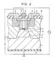
- the electrodes 8serve as gate electrodes of the FET. As illustrated in Figure 2, when voltages are applied to the respective electrodes, depletion regions 12 are formed by a gate bias, and the region of a current to flow through the active layer 3 of the laser device is limited to a part 13.
- a modulation signalis superposed on the gate bias, whereby the laser oscillation can be modulated.
- the stripe width in the active layer of the semiconductor laser deviceis greatly influential on the oscillation mode of the laser.
- the oscillation mode of the lasercan be controlled by controlling the gate bias.
- the semiconductor laser of this inventionincludes the type in which the depletion region extends to the active layer, and the type in which the depletion region does not extend to the active layer. Examples of the former are Embodiments
- Embodiments 4-6belong to the latter.
- the gain of the laseris varied by means of the depletion regions themselves, and hence, a faster modulation than in the prior-art current modulations system is possible.
- the depletion regionsextend to the active layer in which the recombination between electrons and holes develops, the number of electrons within the active layer is forcibly changed by the depletion regions, to change the power of the laser device. This change is much faster than in the system in which the current to be externally supplied is modulated.
- an electroop- tic effect in the active layer as based on the appearance of the depletion regions in the vicinity of the active layerchanges the refractive index of this semiconductor layer.
- Embodiment 4is such an example.
- the change of the refractive indexresults in a change in the effect of optical confinement within the active layer and the power of the laser device can be modulated. This modulation system exploiting the loss of the gain can make the modulation of the laser device faster than the prior-art modulation based on the supplied current.
- a p-type GaAs substratehole density p ⁇ 10 18 /cm 3
- a p-Ga 0.65 Al 0.35 As layerp ⁇ 10 18 /cm 3 , 1.6 ⁇ m thick
- undoped Ga 0.95 Al 0.05 As layer0.1 pm thick
- an n-Ga 0.65 Al 0.35 As layern ⁇ 5x10 18 /cm 3 , 2 ⁇ m thick
- an n-GaAs layer0.2 pm thick
- an Si0 2 film having a thickness of 500 nmwas formed by the CVD (Chemical Vapor Deposition) process.
- the Si0 2 filmwas etched into the shape of stripes being 5 pm wide with the well-known photolithographic technique.
- the semiconductor layers 2, 3, 4 and 7were etched with an etchant which was a mixed solution consisting of phosphoric acid, hydrogen peroxide and water.
- a Ga o . 7 Al o . 3 As layerwas grown as a burying semiconductor layer 5 by relying on the liquid epitaxial growth again. This layer was made a high resistivity (1 k ⁇ cm).
- an insulating film made up of two layers of AI 2 0 3 being 0.2 pm thick and Si0 2 being 0.3 pm thickwas formed by the well-known CVD process.
- Those two parts of the double-layered insulating film which corresponded to gate electrode leading-out portions of the semi- conductor laser device of this inventionwere provided with openings at an interval of 2 pm.
- Etchantswere a mixed solution consisting of hydrogen fluoride and ammonium fluoride (at 1:6 for Si0 2 ) and phosphoric acid (for AI 2 0 3 ).
- the resultant double-layered Si0 2 -AI 2 0 3 filmserved as a mask for selective diffusion.
- Znwas diffused through the openings so as to reach the second cladding layer 4, by the use of the well-known selective diffusion process. Shown at 6 are the Zn diffused regions.
- the double-layered insulating film serving as the mask for the selective diffusionwas removed, and an Si0 2 film 10 having a thickness of 500 nm was formed by the CVD process anew.
- the Si0 2 film 10was provided with openings for leading out electrodes.
- a source lead-out electrode 9an Au-Ge alloy, Ni and Au were evaporated as three layers to a thickness of 0.8 pm.
- Cr-Auwas evaporated for gate electrodes 8. Subsequently, the rear surface of the semiconductor substrate 1 was polished and lightly etched, whereupon a Cr-Au alloy was evaporated as a p-side electrode 11.
- crystal planeswere cloven along planes normal to the traveling direction of a laser beam, to construct an optical resonator.
- the cavity lengthwas made 300 pm.
- the semiconductor laser devicewas oscillated under conditions of an oscillation wavelength of 837 nm and a threshold current of 30 mA. With a D.C. voltage of -1.5 V applied to the gates of the FET, the laser device could be modulated by applying a high-frequency input of 0.5 V. The high-frequency modulation was possible up to about 5 GHz.
- the impurity island regions 6 functioning as the gateswere formed by the diffusion process in the above example, another method, for example, the ion implantation process may well be resorted to.
- the present inventionis not restricted to the GaAs-GaAIAs-based material, but that it can be realized with other semiconductor materials.
- the semiconductor light- emitting device of this inventioncan be realized by a construction to be stated below.
- an InP substrate (Sn-doped, 3x10 18 /cm 3 ) 1 having the (100) plane as its upper surfacewas used.
- an n-type InP layer (Te-doped, n ⁇ 3x10 18 /cm 3 )as a first cladding layer 2 to a thickness of 3 ⁇ m, a p-type In 0.73 Ga 0.27 As 0.59 P 0.41 layer (Zn-doped, p1 x 10 18 /cm 3 ) as an active layer 3 to a thickness of 0.2 ⁇ m a p-type InP layer (Zn-doped, p ⁇ 2x10 18 / cm 3 ) as a second cladding layer 4 to a thickness of 2 pm, and further a p-type In 0.73 Ga 0.27 As 0.59 P 0.41 layer to a thickness of 0.2 pm. Since the last- mentioned layer is necessary for the crystal growth and is
- an impurity such as Si and Snwas diffused to form n-type island regions 6.
- a drain electrode 9 of the FET and gate electrodes 8 thereofwere respectively formed of Cr-Au and Au-Ge-Ni through an insulating layer 10.
- Au-Ge-Niwas evaporated as a source electrode.
- crystal planeswere cloven along planes normal to the traveling direction of the laser beam, to construct an optical resonator.
- the modulationwas possible up to about 5.3 GHz.
- This embodimentgives a modification of the island regions functioning as the gates of the FET. It will be described with reference to Figure 3.
- n-type GaAs substrate (electron density n ⁇ 10 18 /cm 3 ) 14 having the (100) face as its upper surfacethe following layers were formed by the well-known liquid epitaxial growth.
- an insultating film made up of two layers of A1 2 0 3 being 0.2 ⁇ m thick and Si0 2 being 0.3 pm thickwas formed by the well-known CVD (Chemical Vapor Deposition) process.
- Those parts of the double-layered insulating film which corresponded to island regions 17 to construct gate portions of an FETwere provided with openings, and the resultant insulating film was used as a mask for selective diffusion.
- Etchantswere a mixed solution consisting of hydrogen fluoride and ammonium fluoride (at 1:6 for Si0 2 ) and phosphoric acid (for AI 2 0 3 ). Zn was diffused through the openings by the well-known selective diffusion process so that the depth reaches the semiconductor substrate 14.
- island regions of high resistivity 19were formed by the implantation of protons so as to cut off a lateral current path in the semiconductor layer 21.
- a drain electrode 23 and gate electrodes 24were simultaneously formed by evaporating Cr-Au, and Au-Ge-Ni was evaporated as a source electrode 25.
- Shown at 26is an insulating layer. It was as previously stated that an optical resonator was constructed by cleaving crystal faces along planes normal to the traveling direction of a laser beam. In operation, depletion regions 15 were created, so that current was confined.
Landscapes
- Physics & Mathematics (AREA)
- Condensed Matter Physics & Semiconductors (AREA)
- General Physics & Mathematics (AREA)
- Electromagnetism (AREA)
- Optics & Photonics (AREA)
- Geometry (AREA)
- Semiconductor Lasers (AREA)
Description
- This invention provides a novel structure which permits the direct modulation of a semiconductor laser device. Also, this invention provides a novel structure which permits the mode control of a semiconductor laser device.
- Since semiconductor laser devices are small in size and high in efficiency and are capable of fast modulation, the optical communication and various other applications such as data buses and computer links are considered.
- In order to modulate a semiconductor laser device, current pulses of 30-200 mA are usually impressed on the device. However, when the modulation signal obtains a high speed on the order of 1-2 Gbits/sec, it is difficult to produce such fast current pulses and directly modulate the laser device by means of a conventional silicon transistor.
- In recent years, therefore, attempts to employ a GaAs-based material capable of faster modulation and to integrate a laser device and a field- effect transistor (hereinbelow, abbreviated to "FET") have been made. An example is described in a paper by I. Ury et al. contained in Appi. Phys. Lett. 34(7), 1 April 1979, pp. 430-431. Such examples, however, merely integrate the semi- conductor laser and the FET on a single substrate.
- Another prior art device which includes the features set forth in the pre-characterisation part of claim 1 and which thus uses the function of a FET for controlling the current of a semiconductor laser is known from US Patent Specification 3,959,808. That semiconductor laser device is provided, on the same surface on which one of the current injection electrodes is disposed, with additional electrodes which serve to produce depletion regions in the path of the laser current so as to confine the current path.
- The present invention is generally based on the principle known from the above US specification and has for its object to provide a semiconductor laser device which permits an even better control of the laser current path at a reduced width of the overall laser structure.
- This object is met in accordance with the teaching of claim 1. As a result of the impurity island region(s) and the additional provision of a high resistivity layer on both sides of the semi- conductor assembly, the lasing current is confined and the depletion region does not extend unnecessarily so that modulation can be done with high efficiency; at the same time, the impurity island regions can be made small.
- While it is known from US Patent Specification 4,127,792 to provide impurity regions producing depletion zones to confine a current path, this document relates to a luminescent semiconductor device rather than to a laser and discloses neither the presence of a high resistivity layer in cooperation with the impurity island regions nor the extension of the depletion layers to the p-n junction at which the radiation is generated. Summary of the invention
- Figure 1 is a sectional view of a device showing a typical example of this invention. The figure illustrates a section perpendicular to the traveling direction of a laser beam.
- Numeral 1 designates a p-type GaAs substrate, numeral 2 a first cladding layer which is a p-type GaO.7AI0.3As layer,
numeral 3 an n-type GaAs layer which serves as an active layer of a laser device, numeral 4 a second cladding layer which is an n-type Gao.,Alo.3As layer, andnumeral 7 an n-type'GaAs layer. The respective semiconductor layers are successively formed on the GaAs substrate 1. Subsequently, the mesa-etching of selected parts is performed to form a stripe-shaped stacked semiconductor region. Subsequently a GaAs layer ofhigh resistivity 5 is grown on both sides of the stacked semiconductor region. This structure is the so-called BH type structure (Buried Hetero Structure). Needless to say, the relations of the cladding layers and the active layer which constitute the semiconductor laser device portion are made the same as in conventional semicondcutor lasers. That is, the cladding layers have a greater forbidden band gap and a smaller refractive index than the active layer. In addition, the first and second cladding layers have conductivity types opposite to each other. Further, the semiconductor laser device of this example is formed withisland regions 6 of the p-conductivity type for causing depletion regions in the semicondutor layers. For forming the island regions, it may satisfactorily be resorted to such an expedient as selective diffusion and ion implantation.Electrodes insulating layer 10 as lead-out electrodes. - On the other hand, an
electrode 11 is formed on the rear surface of the GaAs substrate 1. Naturally, surfaces perpendicular to the stripe direction are Fabry-Perot reflective surfaces. - The external lead-out electrodes are interconnected so that the
electrode 9 may serve as a source electrode of an FET and that theelectrode 11 may serve as a drain electrode. Theelectrodes 8 serve as gate electrodes of the FET. As illustrated in Figure 2, when voltages are applied to the respective electrodes,depletion regions 12 are formed by a gate bias, and the region of a current to flow through theactive layer 3 of the laser device is limited to apart 13. - In case where the laser beam needs to be modulated, a modulation signal is superposed on the gate bias, whereby the laser oscillation can be modulated.
- The stripe width in the active layer of the semiconductor laser device is greatly influential on the oscillation mode of the laser. According to the semiconductor laser device of this invention, the oscillation mode of the laser can be controlled by controlling the gate bias.
- The semiconductor laser of this invention includes the type in which the depletion region extends to the active layer, and the type in which the depletion region does not extend to the active layer. Examples of the former are Embodiments
- 1-3 to be described later and Embodiments 4-6 belong to the latter.
- The semiconductor laser of this invention has the following advantages:
- (1) Since the laser device and the modulating FET are formed in a manner to be stacked in the vertical direction, the semiconductor laser can be made very small in size.
- (2) The semiconductor laser can be manufactured by the use of the ordinary liquid epitaxial growth, and the manufacturing process is easy.
- (3) A laser device needs, in general, a current of several tens to 100 mA, and an FET to be combined therewith is required to allow such great current and must have a high mutual conductance (gm). Since the vertical FET employed in this invention can freely control the interval of the two gate electrodes, an FET having desired specifications can be realized without hindrance. Accordingly, the required FET is easily obtained, and also the chip size can be made small.
- (4) Unlike the mere integration, the integration in the vertical type is adopted. Therefore, interconnections between the semiconductor laser device and the FET are substantially unnecessary, and parasitic capacitances can be reduced. Further, the type in which the depletion region reaches the active layer has the following features:
- (1) Not only the mere direct modulation, but also the control of a lateral mode is possible because the depletion regions substantially limit the current path.
- (2) The integration of the semiconductor laser device and the FET in the prior art has been made without interconnecting the respective devices externally. Accordingly, the parasitic capacitances and inductances of interconnections have become lower than in case of assembling the separate devices, but the limit of high-frequency modulation characteristics has been determined by the current modulation limit of the laser device. This is approximately 1 GHz-2 GHz.
- In contrast, in this invention, the gain of the laser is varied by means of the depletion regions themselves, and hence, a faster modulation than in the prior-art current modulations system is possible. In the case where the depletion regions extend to the active layer in which the recombination between electrons and holes develops, the number of electrons within the active layer is forcibly changed by the depletion regions, to change the power of the laser device. This change is much faster than in the system in which the current to be externally supplied is modulated.
- Further, even in the case where the depletion regions are short of the active layer, an electroop- tic effect in the active layer as based on the appearance of the depletion regions in the vicinity of the active layer changes the refractive index of this semiconductor layer.
Embodiment 4 is such an example. The change of the refractive index results in a change in the effect of optical confinement within the active layer and the power of the laser device can be modulated. This modulation system exploiting the loss of the gain can make the modulation of the laser device faster than the prior-art modulation based on the supplied current. - Figures 1 and 3 are sectional views each showing a semiconductor laser device of this invention, and
- Figure 2 is a sectional view for explaining the operation of the semiconductor laser device in Figure 1.
- Description will be made with reference to Figure 1.
- On a p-type GaAs substrate (hole density p≈1018/cm3) which has the (100) face as its upper surface, there were grown the respective layers of a p-Ga0.65Al0.35As layer (p~1018/cm3, 1.6 µm thick) 2, and undoped Ga0.95Al0.05As layer (0.1 pm thick) 3, an n-Ga0.65Al0.35As layer (n~5x10¹⁸/cm3, 2 µm thick) 4 and an n-GaAs layer (0.2 pm thick) 7.
- On the surface of the
semiconductor layer 7, an Si02 film having a thickness of 500 nm was formed by the CVD (Chemical Vapor Deposition) process. The Si02 film was etched into the shape of stripes being 5 pm wide with the well-known photolithographic technique. Using the resultant Si02 film as a mask, the semiconductor layers 2, 3, 4 and 7 were etched with an etchant which was a mixed solution consisting of phosphoric acid, hydrogen peroxide and water. - A Gao.7Alo.3As layer was grown as a burying
semiconductor layer 5 by relying on the liquid epitaxial growth again. This layer was made a high resistivity (1 kΩ·cm). - Subsequently, an insulating film made up of two layers of AI203 being 0.2 pm thick and Si02 being 0.3 pm thick was formed by the well-known CVD process. Those two parts of the double-layered insulating film which corresponded to gate electrode leading-out portions of the semi- conductor laser device of this invention were provided with openings at an interval of 2 pm. Etchants were a mixed solution consisting of hydrogen fluoride and ammonium fluoride (at 1:6 for Si02) and phosphoric acid (for AI203). The resultant double-layered Si02-AI203 film served as a mask for selective diffusion. Zn was diffused through the openings so as to reach the
second cladding layer 4, by the use of the well-known selective diffusion process. Shown at 6 are the Zn diffused regions. - The double-layered insulating film serving as the mask for the selective diffusion was removed, and an Si02 film 10 having a thickness of 500 nm was formed by the CVD process anew. Using the conventional photolithography, the Si02 film 10 was provided with openings for leading out electrodes. As a source lead-out
electrode 9, an Au-Ge alloy, Ni and Au were evaporated as three layers to a thickness of 0.8 pm. Cr-Au was evaporated forgate electrodes 8. Subsequently, the rear surface of the semiconductor substrate 1 was polished and lightly etched, whereupon a Cr-Au alloy was evaporated as a p-side electrode 11. - Lastly, crystal planes were cloven along planes normal to the traveling direction of a laser beam, to construct an optical resonator. The cavity length was made 300 pm. The semiconductor laser device was oscillated under conditions of an oscillation wavelength of 837 nm and a threshold current of 30 mA. With a D.C. voltage of -1.5 V applied to the gates of the FET, the laser device could be modulated by applying a high-frequency input of 0.5 V. The high-frequency modulation was possible up to about 5 GHz.
- Although the
impurity island regions 6 functioning as the gates were formed by the diffusion process in the above example, another method, for example, the ion implantation process may well be resorted to. - It is needless to say that the present invention is not restricted to the GaAs-GaAIAs-based material, but that it can be realized with other semiconductor materials.
- By way of example, the semiconductor light- emitting device of this invention can be realized by a construction to be stated below.
- Since the basic process is the same as in the foregoing example, the principal constituents will be briefly described with reference to Figure 1.
- As a semiconductor substrate, an InP substrate (Sn-doped, 3x10¹⁸/cm3) 1 having the (100) plane as its upper surface was used. On the substrate 1, there were formed by the liquid epitaxial growth an n-type InP layer (Te-doped, n≈3x10¹⁸/cm3)as a first cladding layer 2 to a thickness of 3 µm, a p-type In0.73Ga0.27As0.59P0.41 layer (Zn-doped, p=1 x 10¹⁸/cm3) as an
active layer 3 to a thickness of 0.2 µm a p-type InP layer (Zn-doped, p≈2x10¹⁸/ cm3) as asecond cladding layer 4 to a thickness of 2 pm, and further a p-type In0.73Ga0.27As0.59P0.41 layer to a thickness of 0.2 pm. Since the last- mentioned layer is necessary for the crystal growth and is not always necessary for the device structure, it may well be omitted in the process. - For the gate operation of an FET, an impurity such as Si and Sn was diffused to form n-
type island regions 6. - It was the same as in Embodiment 1 that a
drain electrode 9 of the FET andgate electrodes 8 thereof were respectively formed of Cr-Au and Au-Ge-Ni through an insulatinglayer 10. On the rear surface of the semiconductor substrate 1, Au-Ge-Ni was evaporated as a source electrode. Lastly, crystal planes were cloven along planes normal to the traveling direction of the laser beam, to construct an optical resonator. - When the laser device was oscillated at an oscillation wavelength of 1.3 um and a threshold current of 50 mA, the modulation was possible up to about 5.3 GHz.
- This embodiment gives a modification of the island regions functioning as the gates of the FET. It will be described with reference to Figure 3.
- On an n-type GaAs substrate (electron density n≈1018/cm3) 14 having the (100) face as its upper surface, the following layers were formed by the well-known liquid epitaxial growth.
- As a
semiconductor layer 16 serving as a first cladding layer, an n-type Ga0.7Al0.3As layer (n≈5x10¹⁷/cm3) was formed to a thickness of 2 um; as a semiconductor layer'18 serving as an active layer, an n-type GaAs layer (n≈1016/cm3) was formed to a thickness of 0.1 pm; as asemiconductor layer 21 serving as a second cladding layer, a p-type Ga0.7Al0.3As layer (hole density p=5x 10¹⁷/cm3) was formed to a thickness of 1 pm; and as asemiconductor layer 22, a p-type GaAs layer (p≈1x10¹⁸/cm3) was formed to a thickness of 0.3 pm. - Subsequently, an insultating film made up of two layers of A1203 being 0.2 µm thick and Si02 being 0.3 pm thick was formed by the well-known CVD (Chemical Vapor Deposition) process. Those parts of the double-layered insulating film which corresponded to island regions 17 to construct gate portions of an FET were provided with openings, and the resultant insulating film was used as a mask for selective diffusion. Etchants were a mixed solution consisting of hydrogen fluoride and ammonium fluoride (at 1:6 for Si02) and phosphoric acid (for AI203). Zn was diffused through the openings by the well-known selective diffusion process so that the depth reaches the
semiconductor substrate 14. Thereafter, island regions ofhigh resistivity 19 were formed by the implantation of protons so as to cut off a lateral current path in thesemiconductor layer 21. A drain electrode 23 andgate electrodes 24 were simultaneously formed by evaporating Cr-Au, and Au-Ge-Ni was evaporated as asource electrode 25. Shown at 26 is an insulating layer. It was as previously stated that an optical resonator was constructed by cleaving crystal faces along planes normal to the traveling direction of a laser beam. In operation,depletion regions 15 were created, so that current was confined.
Claims (2)
Applications Claiming Priority (2)
| Application Number | Priority Date | Filing Date | Title |
|---|---|---|---|
| JP575580AJPS56104488A (en) | 1980-01-23 | 1980-01-23 | Semiconductor laser element |
| JP5755/80 | 1980-01-23 |
Publications (3)
| Publication Number | Publication Date |
|---|---|
| EP0033137A2 EP0033137A2 (en) | 1981-08-05 |
| EP0033137A3 EP0033137A3 (en) | 1983-05-11 |
| EP0033137B1true EP0033137B1 (en) | 1988-05-04 |
Family
ID=11619928
Family Applications (1)
| Application Number | Title | Priority Date | Filing Date |
|---|---|---|---|
| EP81100461AExpiredEP0033137B1 (en) | 1980-01-23 | 1981-01-22 | Semiconductor laser device |
Country Status (5)
| Country | Link |
|---|---|
| US (1) | US4430741A (en) |
| EP (1) | EP0033137B1 (en) |
| JP (1) | JPS56104488A (en) |
| CA (1) | CA1152624A (en) |
| DE (1) | DE3176735D1 (en) |
Families Citing this family (20)
| Publication number | Priority date | Publication date | Assignee | Title |
|---|---|---|---|---|
| JPS5710992A (en)* | 1980-06-24 | 1982-01-20 | Sumitomo Electric Ind Ltd | Semiconductor device and manufacture therefor |
| GB2111743B (en)* | 1981-08-25 | 1985-11-27 | Handotai Kenkyu Shinkokai | Semiconductor laser |
| US4445218A (en)* | 1981-09-28 | 1984-04-24 | Bell Telephone Laboratories, Incorporated | Semiconductor laser with conductive current mask |
| JPS58106885A (en)* | 1981-12-18 | 1983-06-25 | Matsushita Electric Ind Co Ltd | semiconductor laser |
| JPS58151087A (en)* | 1982-03-03 | 1983-09-08 | Nippon Telegr & Teleph Corp <Ntt> | Semiconductor laser device |
| JPS58182287A (en)* | 1982-04-19 | 1983-10-25 | Sanyo Electric Co Ltd | Double hetero junction type semiconductor laser |
| US4513423A (en)* | 1982-06-04 | 1985-04-23 | The United States Of America As Represented By The Administrator Of The National Aeronautics And Space Administration | Arrangement for damping the resonance in a laser diode |
| JPS5918694A (en)* | 1982-07-22 | 1984-01-31 | Fujitsu Ltd | Optical semiconductor integrated circuit device |
| JPS59222987A (en)* | 1983-06-01 | 1984-12-14 | Matsushita Electric Ind Co Ltd | Compound semiconductor element and manufacture thereof |
| US4631729A (en)* | 1983-12-01 | 1986-12-23 | Trw Inc. | Semiconductor laser structure |
| JPS60154689A (en)* | 1984-01-25 | 1985-08-14 | Hitachi Ltd | Light emitting element and lighr communication equipment using the same |
| GB2154059B (en)* | 1984-01-25 | 1987-10-28 | Hitachi Ltd | Light emitting chip and communication apparatus using the same |
| JPS60216591A (en)* | 1984-04-12 | 1985-10-30 | Matsushita Electric Ind Co Ltd | Semiconductor light emitting element |
| US4884119A (en)* | 1988-04-22 | 1989-11-28 | American Telephone & Telegraph Company | Integrated multiple quantum well photonic and electronic devices |
| US4878222A (en)* | 1988-08-05 | 1989-10-31 | Eastman Kodak Company | Diode laser with improved means for electrically modulating the emitted light beam intensity including turn-on and turn-off and electrically controlling the position of the emitted laser beam spot |
| JPH0834308B2 (en)* | 1988-11-08 | 1996-03-29 | 三菱電機株式会社 | Optoelectronic integrated circuit |
| US4987576A (en)* | 1988-11-30 | 1991-01-22 | Siemens Aktiengesellschaft | Electrically tunable semiconductor laser with ridge waveguide |
| JP2550711B2 (en)* | 1989-06-27 | 1996-11-06 | 三菱電機株式会社 | Semiconductor laser |
| KR100567346B1 (en)* | 2004-03-23 | 2006-04-04 | 학교법인 포항공과대학교 | Al epispheric epitaxial etchant and method of manufacturing semiconductor device using same |
| TW202220315A (en)* | 2020-05-26 | 2022-05-16 | 立陶宛商布羅利思感測科技公司 | Optoelectronic devices with tunable optical mode and carrier distribution in the waveguides |
Citations (2)
| Publication number | Priority date | Publication date | Assignee | Title |
|---|---|---|---|---|
| US3824133A (en)* | 1971-12-02 | 1974-07-16 | Bell Telephone Labor Inc | Fabrication of electrically insulating regions in optical devices by proton bombardment |
| US4127792A (en)* | 1976-06-01 | 1978-11-28 | Mitsubishi Denki Kabushiki Kaisha | Luminescent semiconductor display device including gate control electrodes |
Family Cites Families (7)
| Publication number | Priority date | Publication date | Assignee | Title |
|---|---|---|---|---|
| DE2420517A1 (en)* | 1974-04-27 | 1975-11-06 | Licentia Gmbh | Opto-electronic semiconductor element - has substrate with deposited semiconductor layers of opposite conductivity with substrate dependent pn-junction |
| JPS5628038B2 (en)* | 1974-05-31 | 1981-06-29 | ||
| JPS571912B2 (en)* | 1974-05-31 | 1982-01-13 | ||
| US3959808A (en)* | 1974-09-19 | 1976-05-25 | Northern Electric Company Limited | Variable stripe width semiconductor laser |
| US4152711A (en)* | 1976-04-01 | 1979-05-01 | Mitsubishi Denki Kabuchiki Kaisha | Semiconductor controlled luminescent device |
| US4166278A (en)* | 1978-03-29 | 1979-08-28 | Mitsubishi Denki Kabushiki Kaisha | Semiconductor injection laser device |
| US4217561A (en) | 1978-06-26 | 1980-08-12 | Xerox Corporation | Beam scanning using radiation pattern distortion |
- 1980
- 1980-01-23JPJP575580Apatent/JPS56104488A/enactiveGranted
- 1981
- 1981-01-15USUS06/225,399patent/US4430741A/ennot_activeExpired - Lifetime
- 1981-01-22EPEP81100461Apatent/EP0033137B1/ennot_activeExpired
- 1981-01-22DEDE8181100461Tpatent/DE3176735D1/ennot_activeExpired
- 1981-01-22CACA000369083Apatent/CA1152624A/ennot_activeExpired
Patent Citations (2)
| Publication number | Priority date | Publication date | Assignee | Title |
|---|---|---|---|---|
| US3824133A (en)* | 1971-12-02 | 1974-07-16 | Bell Telephone Labor Inc | Fabrication of electrically insulating regions in optical devices by proton bombardment |
| US4127792A (en)* | 1976-06-01 | 1978-11-28 | Mitsubishi Denki Kabushiki Kaisha | Luminescent semiconductor display device including gate control electrodes |
Also Published As
| Publication number | Publication date |
|---|---|
| US4430741A (en) | 1984-02-07 |
| JPH0156548B2 (en) | 1989-11-30 |
| EP0033137A3 (en) | 1983-05-11 |
| EP0033137A2 (en) | 1981-08-05 |
| JPS56104488A (en) | 1981-08-20 |
| CA1152624A (en) | 1983-08-23 |
| DE3176735D1 (en) | 1988-06-09 |
Similar Documents
| Publication | Publication Date | Title |
|---|---|---|
| EP0033137B1 (en) | Semiconductor laser device | |
| EP0089980B1 (en) | Semiconductor laser with conductive current mask | |
| US6256331B1 (en) | Semiconductor laser device, optical communication system using the same, and method for producing compound semiconductor | |
| US4212020A (en) | Solid state electro-optical devices on a semi-insulating substrate | |
| US4366567A (en) | Semiconductor laser device | |
| US4958202A (en) | Semiconductor light-emitting device and method of manufacturing the same | |
| JPH0553317B2 (en) | ||
| EP0486128A2 (en) | A semiconductor optical device and a fabricating method therefor | |
| US5801071A (en) | Method for producing semiconductor laser diode | |
| US5383216A (en) | Semiconductor laser with light modulator | |
| US5442649A (en) | Semiconductor laser device | |
| US5228048A (en) | Semiconductor laser device | |
| EP0487192B1 (en) | Opto-electronic integrated circuit having a transmitter of long wavelength | |
| US5149670A (en) | Method for producing semiconductor light emitting device | |
| US4941024A (en) | Semiconductor apparatus | |
| US4791647A (en) | Semiconductor laser | |
| US5084410A (en) | Method of manufacturing semiconductor devices | |
| US4377865A (en) | Semiconductor laser | |
| US4517674A (en) | Zinc-diffused narrow stripe AlGaAs/GaAs double heterostructure laser | |
| US5360763A (en) | Method for fabricating an optical semiconductor device | |
| US4521887A (en) | W-shaped diffused stripe GaAs/AlGaAs laser | |
| JP2973215B2 (en) | Semiconductor laser device | |
| JP2555984B2 (en) | Semiconductor laser and manufacturing method thereof | |
| JPH11112096A (en) | Semiconductor laser device and optical communication system using the same | |
| JPH07235725A (en) | Semiconductor laser device and manufacturing method thereof |
Legal Events
| Date | Code | Title | Description |
|---|---|---|---|
| PUAI | Public reference made under article 153(3) epc to a published international application that has entered the european phase | Free format text:ORIGINAL CODE: 0009012 | |
| AK | Designated contracting states | Designated state(s):DE FR GB NL | |
| 17P | Request for examination filed | Effective date:19811015 | |
| PUAF | Information related to the publication of a search report (a3 document) modified or deleted | Free format text:ORIGINAL CODE: 0009199SEPU | |
| D17D | Deferred search report published (deleted) | ||
| PUAL | Search report despatched | Free format text:ORIGINAL CODE: 0009013 | |
| AK | Designated contracting states | Designated state(s):DE FR GB NL | |
| GRAA | (expected) grant | Free format text:ORIGINAL CODE: 0009210 | |
| AK | Designated contracting states | Kind code of ref document:B1 Designated state(s):DE FR GB NL | |
| PG25 | Lapsed in a contracting state [announced via postgrant information from national office to epo] | Ref country code:NL Effective date:19880504 | |
| REF | Corresponds to: | Ref document number:3176735 Country of ref document:DE Date of ref document:19880609 | |
| ET | Fr: translation filed | ||
| NLV1 | Nl: lapsed or annulled due to failure to fulfill the requirements of art. 29p and 29m of the patents act | ||
| PLBE | No opposition filed within time limit | Free format text:ORIGINAL CODE: 0009261 | |
| STAA | Information on the status of an ep patent application or granted ep patent | Free format text:STATUS: NO OPPOSITION FILED WITHIN TIME LIMIT | |
| 26N | No opposition filed | ||
| PGFP | Annual fee paid to national office [announced via postgrant information from national office to epo] | Ref country code:GB Payment date:19940112 Year of fee payment:14 | |
| PGFP | Annual fee paid to national office [announced via postgrant information from national office to epo] | Ref country code:FR Payment date:19940120 Year of fee payment:14 | |
| PGFP | Annual fee paid to national office [announced via postgrant information from national office to epo] | Ref country code:DE Payment date:19940328 Year of fee payment:14 | |
| PG25 | Lapsed in a contracting state [announced via postgrant information from national office to epo] | Ref country code:GB Effective date:19950122 | |
| GBPC | Gb: european patent ceased through non-payment of renewal fee | Effective date:19950122 | |
| PG25 | Lapsed in a contracting state [announced via postgrant information from national office to epo] | Ref country code:FR Effective date:19950929 | |
| PG25 | Lapsed in a contracting state [announced via postgrant information from national office to epo] | Ref country code:DE Effective date:19951003 | |
| REG | Reference to a national code | Ref country code:FR Ref legal event code:ST |