EP0032197B1 - Test procedures for integrated semi-conductor circuits allowing the electric determination of certain tolerances during the photolithographic stages - Google Patents
Test procedures for integrated semi-conductor circuits allowing the electric determination of certain tolerances during the photolithographic stagesDownload PDFInfo
- Publication number
- EP0032197B1 EP0032197B1EP80107638AEP80107638AEP0032197B1EP 0032197 B1EP0032197 B1EP 0032197B1EP 80107638 AEP80107638 AEP 80107638AEP 80107638 AEP80107638 AEP 80107638AEP 0032197 B1EP0032197 B1EP 0032197B1
- Authority
- EP
- European Patent Office
- Prior art keywords
- resistive element
- resistors
- configurations
- semiconductor wafer
- chosen
- Prior art date
- Legal status (The legal status is an assumption and is not a legal conclusion. Google has not performed a legal analysis and makes no representation as to the accuracy of the status listed.)
- Expired
Links
Images


Classifications
- G—PHYSICS
- G03—PHOTOGRAPHY; CINEMATOGRAPHY; ANALOGOUS TECHNIQUES USING WAVES OTHER THAN OPTICAL WAVES; ELECTROGRAPHY; HOLOGRAPHY
- G03F—PHOTOMECHANICAL PRODUCTION OF TEXTURED OR PATTERNED SURFACES, e.g. FOR PRINTING, FOR PROCESSING OF SEMICONDUCTOR DEVICES; MATERIALS THEREFOR; ORIGINALS THEREFOR; APPARATUS SPECIALLY ADAPTED THEREFOR
- G03F7/00—Photomechanical, e.g. photolithographic, production of textured or patterned surfaces, e.g. printing surfaces; Materials therefor, e.g. comprising photoresists; Apparatus specially adapted therefor
- G03F7/70—Microphotolithographic exposure; Apparatus therefor
- G03F7/70483—Information management; Active and passive control; Testing; Wafer monitoring, e.g. pattern monitoring
- G03F7/7055—Exposure light control in all parts of the microlithographic apparatus, e.g. pulse length control or light interruption
- G03F7/70558—Dose control, i.e. achievement of a desired dose
- G—PHYSICS
- G01—MEASURING; TESTING
- G01R—MEASURING ELECTRIC VARIABLES; MEASURING MAGNETIC VARIABLES
- G01R31/00—Arrangements for testing electric properties; Arrangements for locating electric faults; Arrangements for electrical testing characterised by what is being tested not provided for elsewhere
- G01R31/28—Testing of electronic circuits, e.g. by signal tracer
- G01R31/2851—Testing of integrated circuits [IC]
- G01R31/2884—Testing of integrated circuits [IC] using dedicated test connectors, test elements or test circuits on the IC under test
- G—PHYSICS
- G03—PHOTOGRAPHY; CINEMATOGRAPHY; ANALOGOUS TECHNIQUES USING WAVES OTHER THAN OPTICAL WAVES; ELECTROGRAPHY; HOLOGRAPHY
- G03F—PHOTOMECHANICAL PRODUCTION OF TEXTURED OR PATTERNED SURFACES, e.g. FOR PRINTING, FOR PROCESSING OF SEMICONDUCTOR DEVICES; MATERIALS THEREFOR; ORIGINALS THEREFOR; APPARATUS SPECIALLY ADAPTED THEREFOR
- G03F7/00—Photomechanical, e.g. photolithographic, production of textured or patterned surfaces, e.g. printing surfaces; Materials therefor, e.g. comprising photoresists; Apparatus specially adapted therefor
- G03F7/70—Microphotolithographic exposure; Apparatus therefor
- G03F7/70483—Information management; Active and passive control; Testing; Wafer monitoring, e.g. pattern monitoring
- G03F7/70605—Workpiece metrology
- G03F7/70616—Monitoring the printed patterns
- G03F7/70633—Overlay, i.e. relative alignment between patterns printed by separate exposures in different layers, or in the same layer in multiple exposures or stitching
- G—PHYSICS
- G03—PHOTOGRAPHY; CINEMATOGRAPHY; ANALOGOUS TECHNIQUES USING WAVES OTHER THAN OPTICAL WAVES; ELECTROGRAPHY; HOLOGRAPHY
- G03F—PHOTOMECHANICAL PRODUCTION OF TEXTURED OR PATTERNED SURFACES, e.g. FOR PRINTING, FOR PROCESSING OF SEMICONDUCTOR DEVICES; MATERIALS THEREFOR; ORIGINALS THEREFOR; APPARATUS SPECIALLY ADAPTED THEREFOR
- G03F7/00—Photomechanical, e.g. photolithographic, production of textured or patterned surfaces, e.g. printing surfaces; Materials therefor, e.g. comprising photoresists; Apparatus specially adapted therefor
- G03F7/70—Microphotolithographic exposure; Apparatus therefor
- G03F7/70483—Information management; Active and passive control; Testing; Wafer monitoring, e.g. pattern monitoring
- G03F7/70605—Workpiece metrology
- G03F7/70653—Metrology techniques
- G03F7/70658—Electrical testing
- H—ELECTRICITY
- H01—ELECTRIC ELEMENTS
- H01L—SEMICONDUCTOR DEVICES NOT COVERED BY CLASS H10
- H01L22/00—Testing or measuring during manufacture or treatment; Reliability measurements, i.e. testing of parts without further processing to modify the parts as such; Structural arrangements therefor
- H01L22/30—Structural arrangements specially adapted for testing or measuring during manufacture or treatment, or specially adapted for reliability measurements
- H01L22/34—Circuits for electrically characterising or monitoring manufacturing processes, e. g. whole test die, wafers filled with test structures, on-board-devices incorporated on each die, process control monitors or pad structures thereof, devices in scribe line
- H—ELECTRICITY
- H01—ELECTRIC ELEMENTS
- H01L—SEMICONDUCTOR DEVICES NOT COVERED BY CLASS H10
- H01L22/00—Testing or measuring during manufacture or treatment; Reliability measurements, i.e. testing of parts without further processing to modify the parts as such; Structural arrangements therefor
- H01L22/10—Measuring as part of the manufacturing process
- H01L22/12—Measuring as part of the manufacturing process for structural parameters, e.g. thickness, line width, refractive index, temperature, warp, bond strength, defects, optical inspection, electrical measurement of structural dimensions, metallurgic measurement of diffusions
- H—ELECTRICITY
- H01—ELECTRIC ELEMENTS
- H01L—SEMICONDUCTOR DEVICES NOT COVERED BY CLASS H10
- H01L2924/00—Indexing scheme for arrangements or methods for connecting or disconnecting semiconductor or solid-state bodies as covered by H01L24/00
- H01L2924/0001—Technical content checked by a classifier
- H01L2924/0002—Not covered by any one of groups H01L24/00, H01L24/00 and H01L2224/00
Definitions
- the present inventionrelates to the testing and control of semiconductor wafers. It relates more particularly to test methods allowing the electrical determination of certain characteristics such as the image size and overlap tolerances, during the photolithographic steps.
- the masking layers (or masks) used in the manufacture of integrated circuitsare deviate from the specifications desired by the circuit designer, due to unwanted phenomena, such as over-exposure or under-exposure of sensitive resins during the production of said masking layers (or said masks).
- the masking layer (or the mask)has the nominal width of a desired line (W)
- an over-etching or under-etching of the insulating layergives diffused regions which are either too wide or too thin comp edges at nominal (design) width. Lines produced with large variations in width ( ⁇ W) compared to the nominal width (W) can cause reliability problems due to undesirable short circuits or open circuits and must therefore be detected as soon as possible during the process. Manufacturing.
- diffused regionsresistances, lines, capacities, ...) produced through an insulating layer etched according to a desired configuration capable of having tolerances on the dimensions, can lead to components of incorrect values and cause problems during operation.
- the reference FR-A-2 296 852describes a method and a test structure for the determination of the tolerance of dimensions, by measurements, which in certain cases, can be essentially electrical. This process results in a relation in fractional form, the numerator of which consists of a difference of two relatively large quantities. This process is therefore very imprecise.
- a first object of the inventionis to provide test structures and test methods which allow the direct determination of image size tolerances by essentially electrical measurements.
- Another object of the inventionis to replace the visual inspection procedures, which are long, costly and inexpensive. safe, by a test method particularly suitable for automatic testing which makes it very easy to build up statistical databases capable of providing, on demand, slice maps highlighting good or bad blocks.
- Yet another object of the inventionis to provide test structures and a test method which in combination with the previous ones allow the electrical determination of the overlap or alignment tolerances of two superimposed images.
- the present inventiontherefore relates firstly to a test method according to the first claim which allows the determination of the tolerances of image dimensions from electrical measurements.
- the structuresinclude two resistance bridges integrated into a semiconductor substrate typically made of silicon, which when a current is injected along a first diagonal makes it possible to measure a potential difference on the other diagonal, respectively ⁇ V1 and AV2 for each resistance bridge.
- the dimensions of the resistorsare chosen so that the dimensional tolerance is directly related to these measured voltages.
- the dimension tolerance ⁇ Wis linked to the electrical quantities ⁇ V1 and AV2 by a relation of the kind
- the present inventionalso relates to the application of this test method to the measurement of overlap tolerances ⁇ A during the superposition of two images, according to claim 4.
- the present inventionfirst proposes two resistance bridges which allow the determination of the tolerances on the image dimensions which are due to the lithography steps, very numerous in the course of the process for processing semiconductor blocks.
- the dimensions of the resistorsare chosen so that the tolerance sought is a direct function of the voltages which are actually measured.
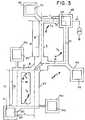
- FIG. 1shows the topology of a first test structure constituted by a first resistance bridge 10 ;
- This figurecan be understood as showing the shape of the P-type resistors implanted or diffused in an N-type silicon substrate, these resistors being formed by the introduction of doping impurities through a masking layer, for example made of Si0 2. according to perfectly known techniques and which will therefore not be detailed here.
- This figurecan also be understood as showing the form of resistors deposited and etched on an insulating layer, and constituted by a material having a sufficient resistivity to allow a measurement of the imbalance of the bridge, for example polycrystalline silicon or metal.
- a symmetrical resistance bridgehaving practically the shape of a rectangle has been chosen.
- the contact regions 13a and 14aare preferably aligned with the second diagonal to reduce the unwanted effects of end resistances of said contacts.
- the shape of these regions of contactis preferably that shown because, this arrangement facilitates the measurement of potentials (a weak current in fact crosses the intermediate regions 13c and 14c). It is therefore on the contacts 11b, 12b, ... that we will apply the test probes (not shown) to explain or measure currents or potentials.
- the resistors R1 and R2respectively have different lengths designated L1 and L2, and the same width designated W.
- the tolerance (or error, or variation) on the dimensions of the width for the lithography stepis given by ⁇ W.
- the masks used to achieve the desired resistive configuration on the silicon waferare generally manufactured from a layer of chromium deposited on a delimited glass plate using the known lithography techniques.
- the over-exposure (or under-exposure) of the resin during the delimitation stepcreates variations in the line width in the configuration of the mask compared to the nominal value desired by the circuit designer.
- over-stripping (or under-stripping) of chromealso adds its own variations.
- variations caused by over-stripping (or under-stripping) of the masking layerIt is all of these variations that ultimately causes this error ⁇ W with respect to the desired nominal width (W).
- Regions 25a and 26acan be added symmetrically to regions 23a and 24a with respect to the second diagonal in order to approximate the potential difference ⁇ V 2 more precisely by averaging
- the tolerance on the image dimension(AW / W) can be obtained from simple electrical measurements.
- FIG. 4shows the topology of the mask corresponding to a test structure which allows the electrical determination of the overlap tolerances.
- the topologyis characterized by the presence of a first image or configuration 41 in the form of an r composed of two parts 41a and 41b and of seven enlarged regions or contact regions 42 to 48 which will allow different electrical measurements to be made later.
- a marker 40is associated with this region.
- the topologyalso includes a second configuration 50 composed of two separate parts 50a and 50b arranged in the form of an r. It also includes a marker 49.
- the element 50awill be aligned with the element 41a but slightly offset in the direction of the Y direction, when the markers 40 and 49 will be aligned and the configurations 41 and 50 will be superimposed.
- the element 50bis parallel to the element 41b but slightly offset in the direction of the X.
- the two configurationsare only necessary if one wishes to know the alignment tolerance along the two axes X and Y.
- the slice of siliconwhich is previously covered with an insulating layer (or resistive: metal or polysilicon) and with a layer of photosensitive resin is exposed successively through configuration 41 then configuration 50. This is obtained simply by the translation of the mask carrying these configurations. If we wanted to include the mask-specific tolerances in the measurement, we would have to use two separate masks, one with configuration 50 and the other configuration 41.
- a structure 52is obtained composed of two resistors 52a and 52b which are shown in FIG. 5 in solid lines. In the case of a resistive layer, these resistances would be obtained directly by selective etching of the resistive layer.
- the resistors 52a and 52bare used to determine the X and Y alignment tolerances respectively.
- the width of these resistorsdepends on the tolerances on the dimensions of the configurations 41 and 50 but also on the misalignment resulting from the superposition of these two configurations. This misalignment is expressed by a so-called alignment tolerance or overlap ⁇ A.
- ⁇ Aalignment tolerance or overlap
- ⁇ W A and ⁇ W Bare obtained from the test structures described using Figures 1 to 3. It is assumed that this calculation is valid, the test structures being close on the silicon wafer. They are in fact carried out either on a specialized block (test site) or on the edge of the block itself (kerf).
- W A and W Bare the widths that are specified by the circuit designer.
- the resistors 52a and 52bcan be replaced by resistance bridges, these can be oriented differently depending on whether it is '' an X or Y misalignment measurement.
Landscapes
- Engineering & Computer Science (AREA)
- Physics & Mathematics (AREA)
- General Physics & Mathematics (AREA)
- Manufacturing & Machinery (AREA)
- Computer Hardware Design (AREA)
- Microelectronics & Electronic Packaging (AREA)
- General Engineering & Computer Science (AREA)
- Automation & Control Theory (AREA)
- Power Engineering (AREA)
- Testing Or Measuring Of Semiconductors Or The Like (AREA)
- Exposure And Positioning Against Photoresist Photosensitive Materials (AREA)
- Semiconductor Integrated Circuits (AREA)
Description
Translated fromFrenchLa présente invention concerne le test et le contrôle des tranches semi-conductrices. Elle concerne plus particulièrement des procédés de test permettant la détermination électrique de certaines caractéristiques telles que les tolérances de dimensions d'images et de recouvrement, lors des étapes photolithographiques.The present invention relates to the testing and control of semiconductor wafers. It relates more particularly to test methods allowing the electrical determination of certain characteristics such as the image size and overlap tolerances, during the photolithographic steps.
Il est bien connu que parmi les très nombreuses étapes de fabrication de circuits intégrés à semi-conducteurs (diffusion, épitaxie, métallurgie, etc...) les étapes de lithographie sont les plus importantes : d'abord parce qu'elles sont très fréquentes, (environ 10 étapes de masquage pour un MOSFET, environ 15 étapes de masquage pour un transistor bipolaire), ensuite parce qu'elles déterminent finalement la densité des circuits. La recherche d'une densité accrue, a développé considérablement ce domaine de la lithographie de l'exposition par radiations ultraviolettes, on est passé à l'exposition par faisceaux électroniques, et par des rayons X. En même temps que les procédés conduisaient à des résolutions de plus en plus"fines (0,5 à 1 micron), ces étapes sont devenues plus critiques. En effet, il est bien connu que les couches de masquage (ou les masques) utilisés dans la fabrication des circuits intégrés, s'écartent des spécifications désirées par le concepteur de circuit, en raison de phénomènes non désirés, tels que la sur-exposition ou la sous-exposition des résines sensibles pendant la fabrication desdites couches de masquages (ou desdits masques). Egalement, on sait aussi que même si la couche de masquage (ou le masque) présente la largeur nominale d'une ligne désirée (W), un sur-décapage ou un sous-décapage de la couche isolante donne des régions diffusées qui sont soit trop larges, soit trop fines comparées à la largeur nominale (de conception). Des lignes réalisées avec des variations importantes de largeurs (ΔW) par rapport à la largeur nominale (W) peuvent poser des problèmes de fiabilité dus, à des court-circuits ou circuits ouverts indésirables et doivent être par conséquent détectées aussitôt que possible durant le procédé de fabrication.It is well known that among the very numerous stages of manufacturing of semiconductor integrated circuits (diffusion, epitaxy, metallurgy, etc.) the lithography stages are the most important: firstly because they are very frequent , (about 10 masking steps for a MOSFET, about 15 masking steps for a bipolar transistor), secondly because they ultimately determine the density of the circuits. The search for increased density has considerably developed this area of lithography of exposure by ultraviolet radiation, we have moved on to exposure by electron beams and by X-rays. At the same time as the processes led to increasingly fine resolutions (0.5 to 1 micron), these steps have become more critical. Indeed, it is well known that the masking layers (or masks) used in the manufacture of integrated circuits, are deviate from the specifications desired by the circuit designer, due to unwanted phenomena, such as over-exposure or under-exposure of sensitive resins during the production of said masking layers (or said masks). Also, it is also known that even if the masking layer (or the mask) has the nominal width of a desired line (W), an over-etching or under-etching of the insulating layer gives diffused regions which are either too wide or too thin comp edges at nominal (design) width. Lines produced with large variations in width (ΔW) compared to the nominal width (W) can cause reliability problems due to undesirable short circuits or open circuits and must therefore be detected as soon as possible during the process. Manufacturing.
Une autre caractéristique importante est que les régions diffusées (résistances, lignes, capacités, ...) réalisées à travers une couche isolante gravée selon une configuration désirée susceptible de présenter des tolérances sur les dimensions, peuvent conduire à des composants de valeurs incorrectes et causer des problèmes lors du fonctionnement.Another important characteristic is that the diffused regions (resistances, lines, capacities, ...) produced through an insulating layer etched according to a desired configuration capable of having tolerances on the dimensions, can lead to components of incorrect values and cause problems during operation.
Il est donc important de maîtriser les défauts d'alignement et autres qui conduisent à des déplacements des images, ces déplacements ou variations (ΔW) exprimant les tolérances de dimension : on recherche une gravure de largeur W, mais on obtient une gravure de largeur ΔW + W (ΔW étant positif ou négatif). La tolérance relative est définie par le rapport ΔW/W.It is therefore important to control the alignment defects and others which lead to displacements of the images, these displacements or variations (ΔW) expressing the dimensional tolerances: an engraving of width W is sought, but an engraving of width ΔW is obtained + W (ΔW being positive or negative). The relative tolerance is defined by the ΔW / W ratio.
Par ailleurs, il est souvent utile de connaître la tolérance de recouvrement ou d'alignement de deux images superposées, cette tolérance est habituellement mesurée et contrôlée visuellement, avec les mêmes inconvénients que ceux indiqués ci-dessus.In addition, it is often useful to know the tolerance of overlap or alignment of two superimposed images, this tolerance is usually measured and checked visually, with the same drawbacks as those indicated above.
La référence FR-A-2 296 852 décrit un procédé et une structure de test pour la détermination de la tolérance de dimensions, par des mesures, qui dans certains cas, peuvent être essentiellement électriques. Ce procédé aboutit à une relation sous forme fractionnaire dont le numérateur est constitué par une différence de deux grandeurs relativement importantes. Ce procédé est donc très imprécis.The reference FR-A-2 296 852 describes a method and a test structure for the determination of the tolerance of dimensions, by measurements, which in certain cases, can be essentially electrical. This process results in a relation in fractional form, the numerator of which consists of a difference of two relatively large quantities. This process is therefore very imprecise.
La référence « Bridge and Van der Paun Sheet Resistors for characterizing the line width of Conducting Layers », J.E.S. Vol. 125, n° 4, avril 1978, pages 650 à 654 se rapporte à un procédé et à des structures de test pour la détermination des largeurs de lignes conductrices. Le problème de la détermination des tolérances de dimensions n'est pas posé et encore moins résolu. Le document « A Four Point Electrical Measurement Technique for Characterizing Mask Superposition errors on S/C Wafers », IEEE, JSSC Vol. SC-13, n° 4, août 1978, pages 436-444 décrit un procédé et une structure de test pour la détermination des erreurs de superposition de masques sur les tranches semi-conductrices à partir de mesures de résistivité de feuille par la classique méthode des quatre points.The reference "Bridge and Van der Paun Sheet Resistors for characterizing the line width of Conducting Layers", J.E.S. Flight. 125, no. 4, April 1978, pages 650 to 654 relates to a method and to test structures for determining the widths of conductive lines. The problem of determining the tolerances of dimensions is not posed and even less solved. The document "A Four Point Electrical Measurement Technique for Characterizing Mask Superposition errors on S / C Wafers", IEEE, JSSC Vol. SC-13, No. 4, August 1978, pages 436-444 describes a method and a test structure for the determination of mask overlap errors on semiconductor wafers from sheet resistivity measurements by the conventional method of the four points.
Enfin la référence publiée dans l'IBM Technical Disclosure Bulletin Vol. 14, n° 12, mai 1972, pages 3707-3708 intitulée : « Dembell Type Resistance Testing Structure », se rapporte à la détermination de la résistivité d'une région base d'un transistor, par la classique méthode des quatre points.Finally, the reference published in the IBM Technical Disclosure Bulletin Vol. 14, n ° 12, May 1972, pages 3707-3708 entitled: "Dembell Type Resistance Testing Structure", relates to the determination of the resistivity of a base region of a transistor, by the classic four point method.
Un premier but de l'invention est de fournir des structures de test et des procédés de test qui permettent la détermination directe des tolérances de dimension d'image grâce à des mesures essentiellement électriques.A first object of the invention is to provide test structures and test methods which allow the direct determination of image size tolerances by essentially electrical measurements.
Un autre but de l'invention est de remplacer les procédés d'inspection visuelle, longs, coûteux et peu sûrs, par un procédé de test particulièrement approprié au test automatique qui permet de constituer très facilement des bases de données statistiques susceptibles de fournir, à la demande, des cartes de tranches mettant en évidence les blocs bons ou mauvais.Another object of the invention is to replace the visual inspection procedures, which are long, costly and inexpensive. safe, by a test method particularly suitable for automatic testing which makes it very easy to build up statistical databases capable of providing, on demand, slice maps highlighting good or bad blocks.
Encore un autre but de l'invention est de fournir des structures de test et un procédé de test qui en combinaison avec les précédents permettent la détermination électrique des tolérances de recouvrement ou d'alignement de deux images superposées.Yet another object of the invention is to provide test structures and a test method which in combination with the previous ones allow the electrical determination of the overlap or alignment tolerances of two superimposed images.
La présente invention concerne donc en premier lieu un procédé de test selon la première revendication qui permet la détermination des tolérances de dimensions d'image à partir de mesures électriques. Les structures comprennent deux ponts de résistances intégrées dans un substrat semiconducteur typiquement en silicium, qui lorsqu'on injecte un courant selon une première diagonale permet de mesurer une différence de potentiel sur l'autre diagonale, respectivement ΔV1 et AV2 pour chaque pont de résistances. Les dimensions des résistances sont choisies de telle sorte que, la tolérance de dimensions soit reliée directement à ces tensions mesurées. Ainsi dans un mode de réalisation préféré, la tolérance de dimension ΔW est reliée aux grandeurs électriques ΔV1 et AV2 par une relation du genreThe present invention therefore relates firstly to a test method according to the first claim which allows the determination of the tolerances of image dimensions from electrical measurements. The structures include two resistance bridges integrated into a semiconductor substrate typically made of silicon, which when a current is injected along a first diagonal makes it possible to measure a potential difference on the other diagonal, respectively ΔV1 and AV2 for each resistance bridge. The dimensions of the resistors are chosen so that the dimensional tolerance is directly related to these measured voltages. Thus in a preferred embodiment, the dimension tolerance ΔW is linked to the electrical quantities ΔV1 and AV2 by a relation of the kind

La présente invention concerne également l'application de ce procédé de test à la mesure des tolérances de recouvrement ΔA lors de la superposition de deux images, selon la revendication 4.The present invention also relates to the application of this test method to the measurement of overlap tolerances ΔA during the superposition of two images, according to claim 4.
Les buts caractéristiques et avantages de la présente invention ressortiront mieux de l'exposé qui suit, fait en référence aux dessins annexés à ce texte, qui représentent un mode de réalisation préféré de celle-ci.The characteristic objects and advantages of the present invention will emerge more clearly from the following description, made with reference to the drawings appended to this text, which represent a preferred embodiment of the latter.
- La figure 1 représente la topologie d'un premier pont de résistances constituant une partie de la structure de test et de contrôle de la tolérance de dimension intégrée sur une tranche de silicium.FIG. 1 represents the topology of a first resistance bridge constituting a part of the test and control structure of the dimension tolerance integrated on a silicon wafer.
- La figure 2 représente la topologie d'un deuxième pont de résistances constituant une autre partie de la structure de test et de contrôle de la tolérance de dimension intégrée sur une tranche de silicium.FIG. 2 represents the topology of a second resistance bridge constituting another part of the test and control structure of the dimension tolerance integrated on a silicon wafer.
- La figure 3 représente une autre structure de test unique combinant en une seule topologie les deux ponts de résistance mentionnés précédemment.FIG. 3 represents another unique test structure combining in a single topology the two resistance bridges mentioned above.
- La figure 4 représente la topologie du masque destiné à permettre la mesure de la tolérance de recouvrement et comportant deux configurations distinctes pour permettre cette mesure selon deux axes perpendiculaires.FIG. 4 represents the topology of the mask intended to allow the measurement of the overlap tolerance and comprising two distinct configurations to allow this measurement according to two perpendicular axes.
- La figure 5 représente la structure de test permettant de mesurer la tolérance de recouvrement, intégrée sur la tranche semi-conductrice après superposition des deux configurations montrées sur la figure 4.FIG. 5 represents the test structure making it possible to measure the overlap tolerance, integrated on the semiconductor wafer after superposition of the two configurations shown in FIG. 4.
La présente invention propose d'abord deux ponts de résistances qui permettent la détermination des tolérances sur les dimensions d'images qui sont dues aux étapes de lithographie, très nombreuses dans le cours du procédé de traitement des blocs semi-conducteurs.The present invention first proposes two resistance bridges which allow the determination of the tolerances on the image dimensions which are due to the lithography steps, very numerous in the course of the process for processing semiconductor blocks.
Les dimensions des résistances sont choisies de telle sorte que la tolérance recherchée soit une fonction directe des tensions qui sont effectivement mesurées.The dimensions of the resistors are chosen so that the tolerance sought is a direct function of the voltages which are actually measured.
Sur la figure 1 on a représenté la topologie d'une première structure de test constituée par un premier pont de résistance 10; Cette figure peut être comprise comme montrant la forme des résistances implantées ou diffusées de type P dans un substrat de silicium de type N, ces résistances étant formées par l'introduction d'impuretés dopantes à travers une couche de masquage, par exemple en Si02 selon des techniques parfaitement connues et qui ne seront donc pas détaillées ici. Cette figure peut être aussi comprise comme montrant la forme de résistances déposées et gravées sur une couche isolante, et constituées par un matériau présentant une résistivité suffisante pour permettre une mesure du déséquilibre du pont par exemple du silicium polycristallin ou du métal. Dans un but de simplification de l'exposé on a choisi un pont de résistance symétrique ayant pratiquement la forme d'un rectangle.FIG. 1 shows the topology of a first test structure constituted by a
Sur les parties élargies (ou régions de contact) qui terminent les extrémités des quatre résistances on distingue d'abord deux régions 11a et 12a, disposées selon une première diagonale dans l'alignement du corps des résistances R1 et R2 qui sont munies de contacts 11b b et 12b, par exemple en aluminium. Le choix de cette forme de contact est préféré pour assurer que les lignes de courant soient parallèles au corps des résistances R1 et R2, et réduire les effets de résistance d'extrémité (RENd. Sur ces contacts on appliquera respectivement un courant I1 et la masse. Deux autres régions 13a et 14a sont disposées selon la seconde diagonale, elles sont également munies de contacts 13b et 14b par exemple en aluminium sur lesquels on viendra mesurer la différence de potentiel aux bornes de ce pont.On the enlarged parts (or contact regions) which terminate the ends of the four resistors, a distinction is first made between two regions 11a and 12a, arranged along a first diagonal in alignment with the body of the resistors R1 and R2 which are provided with
Les régions de contact 13a et 14a sont de préférence alignées avec la seconde diagonale pour réduire les effets non désirés de résistances d'extrémité desdits contacts. La forme de ces régions de contact est de préférence celle représentée car, cette disposition facilite la mesure des potentiels (un faible courant traverse en fait les régions intermédiaires 13c et 14c). C'est donc sur les contacts 11b, 12b, ..., que l'on viendra appliquer les sondes de test (non représentées) pour expliquer ou mesurer des courants ou des potentiels.The
Les résistances R1 et R2 présentent respectivement des longueurs différentes désignées L1 et L2, et une même largeur désignée W. La tolérance (ou erreur, ou variation) sur les dimensions de la largeur pour l'étape de lithographie est donnée par ΔW.The resistors R1 and R2 respectively have different lengths designated L1 and L2, and the same width designated W. The tolerance (or error, or variation) on the dimensions of the width for the lithography step is given by ΔW.
On comprend en effet que les masques utilisés pour réaliser la configuration résistive désirée sur la tranche de silicium sont généralement fabriqués à partir d'une couche de chrome déposée sur une plaque de verre délimitée en utilisant les techniques connues de lithographie. La sur-exposition (ou la sous-exposition) de la résine lors de l'étape de délimitation crée des variations de la largeur de ligne dans la configuration du masque par rapport à la valeur nominale désirée par le concepteur de circuit. En outre le sur-décapage (ou le sous-décapage) du chrome ajoute lui aussi ses propres variations. Enfin il y a les variations provoquées par le sur-décapage (ou le sous-décapage) de la couche de masquage. C'est l'ensemble de ces variations qui provoque finalement cette erreur ΔW par rapport à la largeur nominale désirée (W).It is in fact understood that the masks used to achieve the desired resistive configuration on the silicon wafer are generally manufactured from a layer of chromium deposited on a delimited glass plate using the known lithography techniques. The over-exposure (or under-exposure) of the resin during the delimitation step creates variations in the line width in the configuration of the mask compared to the nominal value desired by the circuit designer. In addition over-stripping (or under-stripping) of chrome also adds its own variations. Finally there are the variations caused by over-stripping (or under-stripping) of the masking layer. It is all of these variations that ultimately causes this error ΔW with respect to the desired nominal width (W).
On peut écrire les équations suivantes, sachant que les deux branches du pont ont la même résistance
on obtient


we obtain
On forme R1-R2 et en tenant compte de (1) on trouve
Cette relation est insuffisante pour fournir le rapport ΔW/W recherché, pour cela il faut utiliser une seconde structure de test également constituée par un second pont de résistance symétrique 20. Cette structure est représentée sur la figure 2. La topologie est assez voisine de celle représentée sur la figure 1. Elle comporte deux parties élargies ou régions de contact 21 a, 22a, selon une première diagonale, munie de contacts 21 b, 22b, par exemple en aluminium auxquels on applique respectivement un courant 12 et la masse. Ces régions élargies ont, de préférence, une partie intermédiaire 21c, 22c, de la forme représentée, qui permet de réduire les effets des tolérances sur les longueurs et sur les largeurs ainsi que les effets de résistance d'extrémité. Les potentiels des régions 23a et 24a disposées sur l'autre diagonale, sont mesurés de façon similaire à partir des contacts 23b et 24b. On peut ajouter des régions 25a et 26a symétriquement aux régions 23a et 24a par rapport à la seconde diagonale dans un but d'approcher la différence de potentiel ΔV2 de façon plus précise en formant la moyenne
En fait on peut écrire
On choisit pour simplifier W'1 = W, L'2 = L2 et L'1 = L1.We choose to simplify W '1 = W, L'2 = L2 and L '1 = L1 .
Avec la topologie des régions intermédiaires retenue on peut estimer qu'il n'y a pas d'erreur ΔL due à la gravure et que les erreurs ΔW et ΔW'2 sont voisines, c'est-à-dire ΔW'2 # ΔW. Par ailleurs, on peut écrire :


La relation ci-dessus peut s'écrire puisque


Le concepteur de circuit peut encore choisir des valeurs préférées pour les paramètres K et K'. Par exemple si K' = 1, c'est-à-dire I1 = 12, les deux structures peuvent très simplement se combiner en une seule structure 30 qui est représentée sur la figure 3 (les références identiques à celles des figures 1 et 2 ont été conservées). Enfin on a choisi K= 2, c'est-à-dire W'2 = 2 W et L2 = 2 L1, ce qui fait que la relation (5) devient
Ainsi avec la structure de test de la figure 3 on peut obtenir la tolérance sur la dimension d'image (AW/W) à partir de simples mesures électriques.
Outre l'intérêt que cette mesure (ΔW/W) présente en soi pour la détermination de la tolérance d'image, facteur important pour l'appréciation de la précision de la gravure, elle peut être également utile pour permettre la détermination des tolérances de recouvrement de deux images superposées.Besides the interest that this measurement (ΔW / W) has in itself for the determination of the image tolerance, an important factor for the appreciation of the engraving precision, it can also be useful to allow the determination of the image tolerances. overlapping of two superimposed images.
Les paramètres des différentes résistances constituant les ponts ont été choisis de façon à simplifier le calcul et permettre l'obtention de ΔW comme une fonction de ΔV1 et ΔV2. On doit cependant remarquer que le principe de l'invention reste applicable à des structures de ponts quelconques, auquel cas ΔW sera en outre fonction desdits paramètres (L1, W1, ...).The parameters of the various resistors constituting the bridges have been chosen so as to simplify the calculation and allow obtaining ΔW as a function of ΔV1 and ΔV2 . It should however be noted that the principle of the invention remains applicable to any bridge structures, in which case ΔW will also be a function of said parameters (L1 , W1 , ...).
La figure 4 montre la topologie du masque correspondant à une structure de test qui permet la détermination électrique des tolérances de recouvrement. La topologie se caractérise par la présence d'une première image ou configuration 41 en forme de r composée de deux parties 41a et 41 b et de sept régions élargies ou régions de contact 42 à 48 qui permettront de procéder à différentes mesures électriques ultérieurement. Un marqueur 40 est associé à cette région. La topologie comprend également une seconde configuration 50 composée de deux parties distinctes 50a et 50b disposées en forme de r. Elle comporte également un marqueur 49. L'élément 50a sera aligné avec l'élément 41a mais légèrement décalé dans le sens de la direction des Y, quand les marqueurs 40 et 49 seront alignés et que les configurations 41 et 50 seront superposées. L'élément 50b est parallèle à l'élément 41 b mais légèrement décalé selon la direction des X. Les deux configurations ne sont nécessaires que si l'on souhaite connaître la tolérance d'alignement selon les deux axes X et Y. La tranche de silicium qui est préalablement recouverte d'une couche isolante (ou résistive : métal ou polysilicium) et d'une couche de résine photosensible est exposée successivement à travers la configuration 41 puis la configuration 50. Ceci est obtenu simplement par la translation du masque portant ces configurations. Si on voulait inclure les tolérances propres au masque dans la mesure il faudrait utiliser deux masques séparés, l'un comportant la configuraton 50 et l'autre la configuration 41.FIG. 4 shows the topology of the mask corresponding to a test structure which allows the electrical determination of the overlap tolerances. The topology is characterized by the presence of a first image or
Ensuite de façon connue, on procède à la gravure puis à l'élimination de la résine. La configuration finale ouverte dans la couche isolante correspond à la superposition des deux configurations. Après implantation dans le substrat silicium d'une impureté dopante d'un type de conductivité opposé à celui du substrat on obtient une structure 52 composée de deux résistances 52a et 52b qui sont montrées sur la figure 5 en traits pleins. Dans le cas d'une couche résistive, ces résistances seraient obtenues directement par gravure sélective de la couche résistive. Les résistances 52a et 52b, servent à déterminer respectivement les tolérances d'alignement en X et en Y.Then in a known manner, the etching is carried out and then the resin is removed. The final configuration opened in the insulating layer corresponds to the superposition of the two configurations. After implantation in the silicon substrate of a doping impurity of a conductivity type opposite to that of the substrate, a
La largeur de ces résistances dépend des tolérances sur les dimensions des configurations 41 et 50 mais également du défaut d'alignement résultant de la superposition de ces deux configurations. Ce défaut d'alignement est exprimé par une tolérance dite d'alignement ou recouvrement ΔA. Quand on connaît les tolérances de dimensions des images, on peut déduire ΔA de la façon suivante : la largeur finale W' dépend des tolérances de dimension d'images sur les configurations 41 soit (ΔWA) et 50 soit (ΔWB) et de la tolérance d'alignement (AA) selon la relation
Les tolérances de dimension des configurations 41 et 50 : ΔWA et ΔWB sont obtenues à partir des structures de test décrites à l'aide des figures 1 à 3. On admet que ce calcul est valable, les structures de test étant voisines sur la tranche de silicium. Elles sont en effet réalisées soit sur un bloc spécialisé (test site) soit sur le bord du bloc lui-même (kerf).The dimensional tolerances of
On a d'après (6)
La relation (7) peut s'écrire :


- mA et mB caractérisent les tolérances de dimension,
- ps est la résistance de feuille de la région implantée ou diffusée
- WA Wc, WD et L sont respectivement des largeurs et une longueur connues du concepteur.
- mA and mB characterize the dimensional tolerances,
- ps is the leaf resistance of the implanted or diffused region
- WA Wc , WD and L are respectively widths and length known to the designer.
On a donc immédiatement à partir d'une simple mesure de résistance et d'un calcul élémentaire la détermination de la tolérance (ou erreur) d'alignement.We therefore immediately have, from a simple resistance measurement and an elementary calculation, the determination of the alignment tolerance (or error).
Enfin pour une meilleure précision et si le nombre de points de test n'est pas un facteur limitatif, les résistances 52a et 52b peuvent être remplacées par des ponts de résistances, ceux-ci pouvant être orientés différemment selon qu'il s'agit d'une mesure de désalignement en X ou en Y.Finally for better accuracy and if the number of test points is not a limiting factor, the
Claims (8)


Applications Claiming Priority (2)
| Application Number | Priority Date | Filing Date | Title |
|---|---|---|---|
| FR8000751 | 1980-01-09 | ||
| FR8000751AFR2473789A1 (en) | 1980-01-09 | 1980-01-09 | TEST METHODS AND STRUCTURES FOR SEMICONDUCTOR INTEGRATED CIRCUITS FOR ELECTRICALLY DETERMINING CERTAIN TOLERANCES DURING PHOTOLITHOGRAPHIC STAGES |
Publications (2)
| Publication Number | Publication Date |
|---|---|
| EP0032197A1 EP0032197A1 (en) | 1981-07-22 |
| EP0032197B1true EP0032197B1 (en) | 1984-04-11 |
Family
ID=9237520
Family Applications (1)
| Application Number | Title | Priority Date | Filing Date |
|---|---|---|---|
| EP80107638AExpiredEP0032197B1 (en) | 1980-01-09 | 1980-12-04 | Test procedures for integrated semi-conductor circuits allowing the electric determination of certain tolerances during the photolithographic stages |
Country Status (4)
| Country | Link |
|---|---|
| US (1) | US4347479A (en) |
| EP (1) | EP0032197B1 (en) |
| DE (1) | DE3067484D1 (en) |
| FR (1) | FR2473789A1 (en) |
Cited By (29)
| Publication number | Priority date | Publication date | Assignee | Title |
|---|---|---|---|---|
| US7570796B2 (en) | 2005-11-18 | 2009-08-04 | Kla-Tencor Technologies Corp. | Methods and systems for utilizing design data in combination with inspection data |
| US7646906B2 (en) | 2004-01-29 | 2010-01-12 | Kla-Tencor Technologies Corp. | Computer-implemented methods for detecting defects in reticle design data |
| US7676077B2 (en) | 2005-11-18 | 2010-03-09 | Kla-Tencor Technologies Corp. | Methods and systems for utilizing design data in combination with inspection data |
| US7689966B2 (en) | 2004-09-14 | 2010-03-30 | Kla-Tencor Technologies Corp. | Methods, systems, and carrier media for evaluating reticle layout data |
| US7711514B2 (en) | 2007-08-10 | 2010-05-04 | Kla-Tencor Technologies Corp. | Computer-implemented methods, carrier media, and systems for generating a metrology sampling plan |
| US7738093B2 (en) | 2007-05-07 | 2010-06-15 | Kla-Tencor Corp. | Methods for detecting and classifying defects on a reticle |
| US7769225B2 (en) | 2005-08-02 | 2010-08-03 | Kla-Tencor Technologies Corp. | Methods and systems for detecting defects in a reticle design pattern |
| US7796804B2 (en) | 2007-07-20 | 2010-09-14 | Kla-Tencor Corp. | Methods for generating a standard reference die for use in a die to standard reference die inspection and methods for inspecting a wafer |
| US7877722B2 (en) | 2006-12-19 | 2011-01-25 | Kla-Tencor Corp. | Systems and methods for creating inspection recipes |
| US7962863B2 (en) | 2007-05-07 | 2011-06-14 | Kla-Tencor Corp. | Computer-implemented methods, systems, and computer-readable media for determining a model for predicting printability of reticle features on a wafer |
| US7975245B2 (en) | 2007-08-20 | 2011-07-05 | Kla-Tencor Corp. | Computer-implemented methods for determining if actual defects are potentially systematic defects or potentially random defects |
| US8041103B2 (en) | 2005-11-18 | 2011-10-18 | Kla-Tencor Technologies Corp. | Methods and systems for determining a position of inspection data in design data space |
| US8112241B2 (en) | 2009-03-13 | 2012-02-07 | Kla-Tencor Corp. | Methods and systems for generating an inspection process for a wafer |
| US8139844B2 (en) | 2008-04-14 | 2012-03-20 | Kla-Tencor Corp. | Methods and systems for determining a defect criticality index for defects on wafers |
| US8194968B2 (en) | 2007-01-05 | 2012-06-05 | Kla-Tencor Corp. | Methods and systems for using electrical information for a device being fabricated on a wafer to perform one or more defect-related functions |
| US8204297B1 (en) | 2009-02-27 | 2012-06-19 | Kla-Tencor Corp. | Methods and systems for classifying defects detected on a reticle |
| US8213704B2 (en) | 2007-05-09 | 2012-07-03 | Kla-Tencor Corp. | Methods and systems for detecting defects in a reticle design pattern |
| US8775101B2 (en) | 2009-02-13 | 2014-07-08 | Kla-Tencor Corp. | Detecting defects on a wafer |
| US8781781B2 (en) | 2010-07-30 | 2014-07-15 | Kla-Tencor Corp. | Dynamic care areas |
| US8826200B2 (en) | 2012-05-25 | 2014-09-02 | Kla-Tencor Corp. | Alteration for wafer inspection |
| US8831334B2 (en) | 2012-01-20 | 2014-09-09 | Kla-Tencor Corp. | Segmentation for wafer inspection |
| US9053527B2 (en) | 2013-01-02 | 2015-06-09 | Kla-Tencor Corp. | Detecting defects on a wafer |
| US9087367B2 (en) | 2011-09-13 | 2015-07-21 | Kla-Tencor Corp. | Determining design coordinates for wafer defects |
| US9092846B2 (en) | 2013-02-01 | 2015-07-28 | Kla-Tencor Corp. | Detecting defects on a wafer using defect-specific and multi-channel information |
| US9134254B2 (en) | 2013-01-07 | 2015-09-15 | Kla-Tencor Corp. | Determining a position of inspection system output in design data space |
| US9170211B2 (en) | 2011-03-25 | 2015-10-27 | Kla-Tencor Corp. | Design-based inspection using repeating structures |
| US9189844B2 (en) | 2012-10-15 | 2015-11-17 | Kla-Tencor Corp. | Detecting defects on a wafer using defect-specific information |
| US9310320B2 (en) | 2013-04-15 | 2016-04-12 | Kla-Tencor Corp. | Based sampling and binning for yield critical defects |
| US9311698B2 (en) | 2013-01-09 | 2016-04-12 | Kla-Tencor Corp. | Detecting defects on a wafer using template image matching |
Families Citing this family (52)
| Publication number | Priority date | Publication date | Assignee | Title |
|---|---|---|---|---|
| US4399205A (en)* | 1981-11-30 | 1983-08-16 | International Business Machines Corporation | Method and apparatus for determining photomask alignment |
| US4538105A (en)* | 1981-12-07 | 1985-08-27 | The Perkin-Elmer Corporation | Overlay test wafer |
| US4516071A (en)* | 1982-07-26 | 1985-05-07 | The United States Of America As Represented By The Administration Of The United States National Aeronautics And Space Administration | Split-cross-bridge resistor for testing for proper fabrication of integrated circuits |
| US4560583A (en)* | 1984-06-29 | 1985-12-24 | International Business Machines Corporation | Resistor design system |
| US4672314A (en)* | 1985-04-12 | 1987-06-09 | Rca Corporation | Comprehensive semiconductor test structure |
| IT1186523B (en)* | 1985-12-31 | 1987-11-26 | Sgs Microelettronica Spa | PROCEDURE FOR THE EVALUATION OF PROCESS PARAMETERS IN THE MANUFACTURE OF SEMICONDUCTOR DEVICES |
| US4855253A (en)* | 1988-01-29 | 1989-08-08 | Hewlett-Packard | Test method for random defects in electronic microstructures |
| US4918377A (en)* | 1988-12-05 | 1990-04-17 | The United States Of America As Represented By The Administrator Of The National Aeronautics And Space Administration | Integrated circuit reliability testing |
| US5044750A (en)* | 1990-08-13 | 1991-09-03 | National Semiconductor Corporation | Method for checking lithography critical dimensions |
| US5082792A (en)* | 1990-08-15 | 1992-01-21 | Lsi Logic Corporation | Forming a physical structure on an integrated circuit device and determining its size by measurement of resistance |
| JP3017871B2 (en)* | 1991-01-02 | 2000-03-13 | テキサス インスツルメンツ インコーポレイテツド | Variation detection circuit on chip for IC device |
| US5254941A (en)* | 1991-10-29 | 1993-10-19 | Sgs-Thomson Microelectronics, Inc. | Structure and method for determining isolation of integrated circuit |
| US5247262A (en)* | 1992-03-13 | 1993-09-21 | The United States Of America As Represented By The Secretary Of Commerce | Linewidth micro-bridge test structure |
| US5373232A (en)* | 1992-03-13 | 1994-12-13 | The United States Of America As Represented By The Secretary Of Commerce | Method of and articles for accurately determining relative positions of lithographic artifacts |
| US5857258A (en)* | 1992-03-13 | 1999-01-12 | The United States Of America As Represented By The Secretary Of Commerce | Electrical test structure and method for measuring the relative locations of conductive features on an insulating substrate |
| FR2696009A1 (en)* | 1992-09-23 | 1994-03-25 | Philips Electronique Lab | Calibration device for microwave adjustment of the reference planes of an apparatus for measuring the dispersion parameters of integrated circuit elements. |
| US5370923A (en)* | 1993-02-26 | 1994-12-06 | Advanced Micro Devices, Inc. | Photolithography test structure |
| TW248612B (en)* | 1993-03-31 | 1995-06-01 | Siemens Ag | |
| US5552718A (en)* | 1995-01-04 | 1996-09-03 | International Business Machines Corp. | Electrical test structure and method for space and line measurement |
| US5670891A (en)* | 1995-06-07 | 1997-09-23 | Advanced Micro Devices, Inc. | Structures to extract defect size information of poly and source-drain semiconductor devices and method for making the same |
| US6001663A (en)* | 1995-06-07 | 1999-12-14 | Advanced Micro Devices, Inc. | Apparatus for detecting defect sizes in polysilicon and source-drain semiconductor devices and method for making the same |
| KR100223924B1 (en)* | 1996-07-19 | 1999-10-15 | 구본준 | Test pattern for measuring the line width of an electrode |
| US5963784A (en)* | 1997-05-09 | 1999-10-05 | Vlsi Technology, Inc. | Methods of determining parameters of a semiconductor device and the width of an insulative spacer of a semiconductor device |
| US6380554B1 (en)* | 1998-06-08 | 2002-04-30 | Advanced Micro Devices, Inc. | Test structure for electrically measuring the degree of misalignment between successive layers of conductors |
| KR100273317B1 (en)* | 1998-11-04 | 2000-12-15 | 김영환 | Test pattern structure for measuring a misalignment in semiconductor device fabrication process and method of measuring the misalignment |
| US6268717B1 (en)* | 1999-03-04 | 2001-07-31 | Advanced Micro Devices, Inc. | Semiconductor test structure with intentional partial defects and method of use |
| US6452412B1 (en) | 1999-03-04 | 2002-09-17 | Advanced Micro Devices, Inc. | Drop-in test structure and methodology for characterizing an integrated circuit process flow and topography |
| US6297644B1 (en) | 1999-03-04 | 2001-10-02 | Advanced Micro Devices, Inc. | Multipurpose defect test structure with switchable voltage contrast capability and method of use |
| US6429667B1 (en)* | 2000-06-19 | 2002-08-06 | International Business Machines Corporation | Electrically testable process window monitor for lithographic processing |
| US6844751B2 (en) | 2000-09-30 | 2005-01-18 | Texas Instruments Incorporated | Multi-state test structures and methods |
| US6392251B1 (en)* | 2000-10-17 | 2002-05-21 | Advanced Micro Devices, Inc. | Test structures for identifying open contacts and methods of making the same |
| US6559476B2 (en)* | 2001-06-26 | 2003-05-06 | United Microelectronics Corp. | Method and structure for measuring bridge induced by mask layout amendment |
| US6716559B2 (en)* | 2001-12-13 | 2004-04-06 | International Business Machines Corporation | Method and system for determining overlay tolerance |
| US6570228B1 (en)* | 2002-01-17 | 2003-05-27 | Advanced Micro Devices, Inc. | Method and apparatus for electrically measuring insulating film thickness |
| US6620635B2 (en) | 2002-02-20 | 2003-09-16 | International Business Machines Corporation | Damascene resistor and method for measuring the width of same |
| DE10214885C1 (en)* | 2002-04-04 | 2003-11-20 | Infineon Technologies Ag | Method and test structure for determining resistance values on several interconnected resistors in an integrated circuit |
| JP3652671B2 (en)* | 2002-05-24 | 2005-05-25 | 沖電気工業株式会社 | Wiring pattern for measurement and measuring method thereof |
| US7084427B2 (en)* | 2003-06-10 | 2006-08-01 | International Business Machines Corporation | Systems and methods for overlay shift determination |
| JP4242796B2 (en)* | 2004-03-12 | 2009-03-25 | パナソニック株式会社 | Image recognition method and image recognition apparatus |
| JP4975972B2 (en)* | 2005-03-15 | 2012-07-11 | 日立オートモティブシステムズ株式会社 | Physical quantity sensor |
| KR100828512B1 (en)* | 2005-10-11 | 2008-05-13 | 삼성전기주식회사 | semiconductor chip package capable of monitoring open and short at once |
| US7750660B2 (en)* | 2006-03-30 | 2010-07-06 | Qualcomm Incorporated | Integrated circuit with improved test capability via reduced pin count |
| US8063401B2 (en)* | 2006-08-17 | 2011-11-22 | Nxp B.V. | Testing for correct undercutting of an electrode during an etching step |
| CN100579894C (en)* | 2007-10-12 | 2010-01-13 | 东南大学 | Electrical Test Structure for Alignment Error between Metal Layer and Insulation Layer in Micro-Electro-Mechanical Device Processing |
| CN100542947C (en)* | 2007-10-12 | 2009-09-23 | 东南大学 | Electrical Test Structure for Alignment Error of Patterns of Different Conductive Layers in MEMS Device Processing |
| US8258806B2 (en) | 2007-12-24 | 2012-09-04 | Texas Instruments Incorporated | Self-isolating mixed design-rule integrated yield monitor |
| US9659670B2 (en) | 2008-07-28 | 2017-05-23 | Kla-Tencor Corp. | Computer-implemented methods, computer-readable media, and systems for classifying defects detected in a memory device area on a wafer |
| US9252202B2 (en)* | 2011-08-23 | 2016-02-02 | Wafertech, Llc | Test structure and method for determining overlay accuracy in semiconductor devices using resistance measurement |
| JP6110113B2 (en)* | 2012-11-20 | 2017-04-05 | 株式会社日本マイクロニクス | Multilayer wiring board and manufacturing method thereof |
| US9865512B2 (en) | 2013-04-08 | 2018-01-09 | Kla-Tencor Corp. | Dynamic design attributes for wafer inspection |
| JP6372097B2 (en)* | 2014-03-07 | 2018-08-15 | 株式会社リコー | Detection device, detection circuit, sensor module, and image forming apparatus |
| US10078107B2 (en) | 2015-10-27 | 2018-09-18 | Globalfoundries Inc. | Wafer level electrical test for optical proximity correction and/or etch bias |
Family Cites Families (2)
| Publication number | Priority date | Publication date | Assignee | Title |
|---|---|---|---|---|
| CA997481A (en)* | 1972-12-29 | 1976-09-21 | International Business Machines Corporation | Dc testing of integrated circuits and a novel integrated circuit structure to facilitate such testing |
| US3974443A (en)* | 1975-01-02 | 1976-08-10 | International Business Machines Corporation | Conductive line width and resistivity measuring system |
- 1980
- 1980-01-09FRFR8000751Apatent/FR2473789A1/enactivePending
- 1980-11-24USUS06/210,081patent/US4347479A/ennot_activeExpired - Lifetime
- 1980-12-04EPEP80107638Apatent/EP0032197B1/ennot_activeExpired
- 1980-12-04DEDE8080107638Tpatent/DE3067484D1/ennot_activeExpired
Cited By (32)
| Publication number | Priority date | Publication date | Assignee | Title |
|---|---|---|---|---|
| US7646906B2 (en) | 2004-01-29 | 2010-01-12 | Kla-Tencor Technologies Corp. | Computer-implemented methods for detecting defects in reticle design data |
| US7689966B2 (en) | 2004-09-14 | 2010-03-30 | Kla-Tencor Technologies Corp. | Methods, systems, and carrier media for evaluating reticle layout data |
| US7769225B2 (en) | 2005-08-02 | 2010-08-03 | Kla-Tencor Technologies Corp. | Methods and systems for detecting defects in a reticle design pattern |
| US8041103B2 (en) | 2005-11-18 | 2011-10-18 | Kla-Tencor Technologies Corp. | Methods and systems for determining a position of inspection data in design data space |
| US7676077B2 (en) | 2005-11-18 | 2010-03-09 | Kla-Tencor Technologies Corp. | Methods and systems for utilizing design data in combination with inspection data |
| US7570796B2 (en) | 2005-11-18 | 2009-08-04 | Kla-Tencor Technologies Corp. | Methods and systems for utilizing design data in combination with inspection data |
| US8139843B2 (en) | 2005-11-18 | 2012-03-20 | Kla-Tencor Technologies Corp. | Methods and systems for utilizing design data in combination with inspection data |
| US8923600B2 (en) | 2005-11-18 | 2014-12-30 | Kla-Tencor Technologies Corp. | Methods and systems for utilizing design data in combination with inspection data |
| US7877722B2 (en) | 2006-12-19 | 2011-01-25 | Kla-Tencor Corp. | Systems and methods for creating inspection recipes |
| US8194968B2 (en) | 2007-01-05 | 2012-06-05 | Kla-Tencor Corp. | Methods and systems for using electrical information for a device being fabricated on a wafer to perform one or more defect-related functions |
| US7962863B2 (en) | 2007-05-07 | 2011-06-14 | Kla-Tencor Corp. | Computer-implemented methods, systems, and computer-readable media for determining a model for predicting printability of reticle features on a wafer |
| US7738093B2 (en) | 2007-05-07 | 2010-06-15 | Kla-Tencor Corp. | Methods for detecting and classifying defects on a reticle |
| US8213704B2 (en) | 2007-05-09 | 2012-07-03 | Kla-Tencor Corp. | Methods and systems for detecting defects in a reticle design pattern |
| US7796804B2 (en) | 2007-07-20 | 2010-09-14 | Kla-Tencor Corp. | Methods for generating a standard reference die for use in a die to standard reference die inspection and methods for inspecting a wafer |
| US8204296B2 (en) | 2007-07-20 | 2012-06-19 | Kla-Tencor Corp. | Methods for generating a standard reference die for use in a die to standard reference die inspection and methods for inspecting a wafer |
| US7711514B2 (en) | 2007-08-10 | 2010-05-04 | Kla-Tencor Technologies Corp. | Computer-implemented methods, carrier media, and systems for generating a metrology sampling plan |
| US7975245B2 (en) | 2007-08-20 | 2011-07-05 | Kla-Tencor Corp. | Computer-implemented methods for determining if actual defects are potentially systematic defects or potentially random defects |
| US8139844B2 (en) | 2008-04-14 | 2012-03-20 | Kla-Tencor Corp. | Methods and systems for determining a defect criticality index for defects on wafers |
| US8775101B2 (en) | 2009-02-13 | 2014-07-08 | Kla-Tencor Corp. | Detecting defects on a wafer |
| US8204297B1 (en) | 2009-02-27 | 2012-06-19 | Kla-Tencor Corp. | Methods and systems for classifying defects detected on a reticle |
| US8112241B2 (en) | 2009-03-13 | 2012-02-07 | Kla-Tencor Corp. | Methods and systems for generating an inspection process for a wafer |
| US8781781B2 (en) | 2010-07-30 | 2014-07-15 | Kla-Tencor Corp. | Dynamic care areas |
| US9170211B2 (en) | 2011-03-25 | 2015-10-27 | Kla-Tencor Corp. | Design-based inspection using repeating structures |
| US9087367B2 (en) | 2011-09-13 | 2015-07-21 | Kla-Tencor Corp. | Determining design coordinates for wafer defects |
| US8831334B2 (en) | 2012-01-20 | 2014-09-09 | Kla-Tencor Corp. | Segmentation for wafer inspection |
| US8826200B2 (en) | 2012-05-25 | 2014-09-02 | Kla-Tencor Corp. | Alteration for wafer inspection |
| US9189844B2 (en) | 2012-10-15 | 2015-11-17 | Kla-Tencor Corp. | Detecting defects on a wafer using defect-specific information |
| US9053527B2 (en) | 2013-01-02 | 2015-06-09 | Kla-Tencor Corp. | Detecting defects on a wafer |
| US9134254B2 (en) | 2013-01-07 | 2015-09-15 | Kla-Tencor Corp. | Determining a position of inspection system output in design data space |
| US9311698B2 (en) | 2013-01-09 | 2016-04-12 | Kla-Tencor Corp. | Detecting defects on a wafer using template image matching |
| US9092846B2 (en) | 2013-02-01 | 2015-07-28 | Kla-Tencor Corp. | Detecting defects on a wafer using defect-specific and multi-channel information |
| US9310320B2 (en) | 2013-04-15 | 2016-04-12 | Kla-Tencor Corp. | Based sampling and binning for yield critical defects |
Also Published As
| Publication number | Publication date |
|---|---|
| US4347479A (en) | 1982-08-31 |
| FR2473789A1 (en) | 1981-07-17 |
| DE3067484D1 (en) | 1984-05-17 |
| EP0032197A1 (en) | 1981-07-22 |
Similar Documents
| Publication | Publication Date | Title |
|---|---|---|
| EP0032197B1 (en) | Test procedures for integrated semi-conductor circuits allowing the electric determination of certain tolerances during the photolithographic stages | |
| US5898478A (en) | Method of using a test reticle to optimize alignment of integrated circuit process layers | |
| US5167778A (en) | Electrochemical etching method | |
| FR2726960A1 (en) | PROCESS FOR PRODUCING MAGNETORESISTIVE TRANSDUCERS | |
| US4100486A (en) | Monitor for semiconductor diffusion operations | |
| JPS5816548B2 (en) | Method for selectively metallizing microelectronic devices | |
| US4529314A (en) | Method of measuring misalignment between levels on a substrate | |
| JPS5893326A (en) | Method of measuring performance of exposure device | |
| EP0578899A1 (en) | Process for measuring the planarity degree of a dielectric layer in an integrated circuit and integrated circuit including means for performing said process | |
| US4943710A (en) | Image sensor and manufacturing method for the same | |
| US4766085A (en) | Method of manufacturing contact type one-dimensional image sensor | |
| JPS62135838A (en) | Pattern forming method and device | |
| US4462881A (en) | Method of forming a multilayer thin film | |
| FR2659495A1 (en) | ELASTOMERIC CONNECTOR FOR INTEGRATED CIRCUITS OR THE LIKE, AND MANUFACTURING METHOD THEREOF. | |
| US7217946B2 (en) | Method for making a wire nanostructure in a semiconductor film | |
| CA1223654A (en) | Integrated photo-responsive metal oxide semiconductor circuit | |
| JP2765244B2 (en) | Magnetoresistive element and method of manufacturing the same | |
| JP3249218B2 (en) | How to detect resist scum | |
| KR960002487B1 (en) | Manufacturing method of magnetoresistive element | |
| GB2386962A (en) | Method for manufacturing a thin film assembly | |
| JPH088225A (en) | Method for inspecting dimension of conductor pattern of semiconductor device | |
| JPH0317215B2 (en) | ||
| JPS59178741A (en) | Wafer for seemiconductor integrated circuit element | |
| Allen et al. | Junction-isolated electrical test structures for critical dimension calibration standards | |
| JPS59121966A (en) | Manufacturing method of semiconductor device |
Legal Events
| Date | Code | Title | Description |
|---|---|---|---|
| PUAI | Public reference made under article 153(3) epc to a published international application that has entered the european phase | Free format text:ORIGINAL CODE: 0009012 | |
| AK | Designated contracting states | Designated state(s):DE FR GB | |
| 17P | Request for examination filed | Effective date:19810828 | |
| GRAA | (expected) grant | Free format text:ORIGINAL CODE: 0009210 | |
| AK | Designated contracting states | Designated state(s):DE FR GB | |
| REF | Corresponds to: | Ref document number:3067484 Country of ref document:DE Date of ref document:19840517 | |
| PLBE | No opposition filed within time limit | Free format text:ORIGINAL CODE: 0009261 | |
| STAA | Information on the status of an ep patent application or granted ep patent | Free format text:STATUS: NO OPPOSITION FILED WITHIN TIME LIMIT | |
| 26N | No opposition filed | ||
| PGFP | Annual fee paid to national office [announced via postgrant information from national office to epo] | Ref country code:GB Payment date:19901119 Year of fee payment:11 | |
| PGFP | Annual fee paid to national office [announced via postgrant information from national office to epo] | Ref country code:DE Payment date:19901231 Year of fee payment:11 | |
| PGFP | Annual fee paid to national office [announced via postgrant information from national office to epo] | Ref country code:FR Payment date:19911127 Year of fee payment:12 | |
| PG25 | Lapsed in a contracting state [announced via postgrant information from national office to epo] | Ref country code:GB Effective date:19911204 | |
| GBPC | Gb: european patent ceased through non-payment of renewal fee | ||
| PG25 | Lapsed in a contracting state [announced via postgrant information from national office to epo] | Ref country code:DE Effective date:19920901 | |
| PG25 | Lapsed in a contracting state [announced via postgrant information from national office to epo] | Ref country code:FR Effective date:19930831 | |
| REG | Reference to a national code | Ref country code:FR Ref legal event code:ST |