DE20321881U1 - LEDS with vertical structure - Google Patents
LEDS with vertical structureDownload PDFInfo
- Publication number
- DE20321881U1 DE20321881U1DE20321881UDE20321881UDE20321881U1DE 20321881 U1DE20321881 U1DE 20321881U1DE 20321881 UDE20321881 UDE 20321881UDE 20321881 UDE20321881 UDE 20321881UDE 20321881 U1DE20321881 U1DE 20321881U1
- Authority
- DE
- Germany
- Prior art keywords
- layer
- type
- emitting device
- light
- electrode
- Prior art date
- Legal status (The legal status is an assumption and is not a legal conclusion. Google has not performed a legal analysis and makes no representation as to the accuracy of the status listed.)
- Expired - Lifetime
Links
Images


Classifications
- H—ELECTRICITY
- H10—SEMICONDUCTOR DEVICES; ELECTRIC SOLID-STATE DEVICES NOT OTHERWISE PROVIDED FOR
- H10H—INORGANIC LIGHT-EMITTING SEMICONDUCTOR DEVICES HAVING POTENTIAL BARRIERS
- H10H20/00—Individual inorganic light-emitting semiconductor devices having potential barriers, e.g. light-emitting diodes [LED]
- H10H20/80—Constructional details
- H10H20/81—Bodies
- H10H20/815—Bodies having stress relaxation structures, e.g. buffer layers
- H—ELECTRICITY
- H01—ELECTRIC ELEMENTS
- H01C—RESISTORS
- H01C7/00—Non-adjustable resistors formed as one or more layers or coatings; Non-adjustable resistors made from powdered conducting material or powdered semi-conducting material with or without insulating material
- H01C7/006—Thin film resistors
- H—ELECTRICITY
- H01—ELECTRIC ELEMENTS
- H01C—RESISTORS
- H01C7/00—Non-adjustable resistors formed as one or more layers or coatings; Non-adjustable resistors made from powdered conducting material or powdered semi-conducting material with or without insulating material
- H01C7/008—Thermistors
- H—ELECTRICITY
- H10—SEMICONDUCTOR DEVICES; ELECTRIC SOLID-STATE DEVICES NOT OTHERWISE PROVIDED FOR
- H10D—INORGANIC ELECTRIC SEMICONDUCTOR DEVICES
- H10D1/00—Resistors, capacitors or inductors
- H10D1/40—Resistors
- H10D1/47—Resistors having no potential barriers
- H—ELECTRICITY
- H10—SEMICONDUCTOR DEVICES; ELECTRIC SOLID-STATE DEVICES NOT OTHERWISE PROVIDED FOR
- H10D—INORGANIC ELECTRIC SEMICONDUCTOR DEVICES
- H10D84/00—Integrated devices formed in or on semiconductor substrates that comprise only semiconducting layers, e.g. on Si wafers or on GaAs-on-Si wafers
- H10D84/201—Integrated devices formed in or on semiconductor substrates that comprise only semiconducting layers, e.g. on Si wafers or on GaAs-on-Si wafers characterised by the integration of only components covered by H10D1/00 or H10D8/00, e.g. RLC circuits
- H10D84/204—Integrated devices formed in or on semiconductor substrates that comprise only semiconducting layers, e.g. on Si wafers or on GaAs-on-Si wafers characterised by the integration of only components covered by H10D1/00 or H10D8/00, e.g. RLC circuits of combinations of diodes or capacitors or resistors
- H10D84/209—Integrated devices formed in or on semiconductor substrates that comprise only semiconducting layers, e.g. on Si wafers or on GaAs-on-Si wafers characterised by the integration of only components covered by H10D1/00 or H10D8/00, e.g. RLC circuits of combinations of diodes or capacitors or resistors of only resistors
- H—ELECTRICITY
- H10—SEMICONDUCTOR DEVICES; ELECTRIC SOLID-STATE DEVICES NOT OTHERWISE PROVIDED FOR
- H10H—INORGANIC LIGHT-EMITTING SEMICONDUCTOR DEVICES HAVING POTENTIAL BARRIERS
- H10H20/00—Individual inorganic light-emitting semiconductor devices having potential barriers, e.g. light-emitting diodes [LED]
- H10H20/01—Manufacture or treatment
- H10H20/011—Manufacture or treatment of bodies, e.g. forming semiconductor layers
- H10H20/013—Manufacture or treatment of bodies, e.g. forming semiconductor layers having light-emitting regions comprising only Group III-V materials
- H10H20/0133—Manufacture or treatment of bodies, e.g. forming semiconductor layers having light-emitting regions comprising only Group III-V materials with a substrate not being Group III-V materials
- H10H20/01335—Manufacture or treatment of bodies, e.g. forming semiconductor layers having light-emitting regions comprising only Group III-V materials with a substrate not being Group III-V materials the light-emitting regions comprising nitride materials
- H—ELECTRICITY
- H10—SEMICONDUCTOR DEVICES; ELECTRIC SOLID-STATE DEVICES NOT OTHERWISE PROVIDED FOR
- H10H—INORGANIC LIGHT-EMITTING SEMICONDUCTOR DEVICES HAVING POTENTIAL BARRIERS
- H10H20/00—Individual inorganic light-emitting semiconductor devices having potential barriers, e.g. light-emitting diodes [LED]
- H10H20/01—Manufacture or treatment
- H10H20/011—Manufacture or treatment of bodies, e.g. forming semiconductor layers
- H10H20/018—Bonding of wafers
- H—ELECTRICITY
- H10—SEMICONDUCTOR DEVICES; ELECTRIC SOLID-STATE DEVICES NOT OTHERWISE PROVIDED FOR
- H10H—INORGANIC LIGHT-EMITTING SEMICONDUCTOR DEVICES HAVING POTENTIAL BARRIERS
- H10H20/00—Individual inorganic light-emitting semiconductor devices having potential barriers, e.g. light-emitting diodes [LED]
- H10H20/80—Constructional details
- H10H20/81—Bodies
- H10H20/811—Bodies having quantum effect structures or superlattices, e.g. tunnel junctions
- H10H20/812—Bodies having quantum effect structures or superlattices, e.g. tunnel junctions within the light-emitting regions, e.g. having quantum confinement structures
- H—ELECTRICITY
- H10—SEMICONDUCTOR DEVICES; ELECTRIC SOLID-STATE DEVICES NOT OTHERWISE PROVIDED FOR
- H10H—INORGANIC LIGHT-EMITTING SEMICONDUCTOR DEVICES HAVING POTENTIAL BARRIERS
- H10H20/00—Individual inorganic light-emitting semiconductor devices having potential barriers, e.g. light-emitting diodes [LED]
- H10H20/80—Constructional details
- H10H20/81—Bodies
- H10H20/822—Materials of the light-emitting regions
- H10H20/824—Materials of the light-emitting regions comprising only Group III-V materials, e.g. GaP
- H10H20/825—Materials of the light-emitting regions comprising only Group III-V materials, e.g. GaP containing nitrogen, e.g. GaN
- H—ELECTRICITY
- H10—SEMICONDUCTOR DEVICES; ELECTRIC SOLID-STATE DEVICES NOT OTHERWISE PROVIDED FOR
- H10H—INORGANIC LIGHT-EMITTING SEMICONDUCTOR DEVICES HAVING POTENTIAL BARRIERS
- H10H20/00—Individual inorganic light-emitting semiconductor devices having potential barriers, e.g. light-emitting diodes [LED]
- H10H20/80—Constructional details
- H10H20/83—Electrodes
- H10H20/831—Electrodes characterised by their shape
- H—ELECTRICITY
- H10—SEMICONDUCTOR DEVICES; ELECTRIC SOLID-STATE DEVICES NOT OTHERWISE PROVIDED FOR
- H10H—INORGANIC LIGHT-EMITTING SEMICONDUCTOR DEVICES HAVING POTENTIAL BARRIERS
- H10H20/00—Individual inorganic light-emitting semiconductor devices having potential barriers, e.g. light-emitting diodes [LED]
- H10H20/80—Constructional details
- H10H20/83—Electrodes
- H10H20/832—Electrodes characterised by their material
- H—ELECTRICITY
- H10—SEMICONDUCTOR DEVICES; ELECTRIC SOLID-STATE DEVICES NOT OTHERWISE PROVIDED FOR
- H10H—INORGANIC LIGHT-EMITTING SEMICONDUCTOR DEVICES HAVING POTENTIAL BARRIERS
- H10H20/00—Individual inorganic light-emitting semiconductor devices having potential barriers, e.g. light-emitting diodes [LED]
- H10H20/80—Constructional details
- H10H20/84—Coatings, e.g. passivation layers or antireflective coatings
- H—ELECTRICITY
- H10—SEMICONDUCTOR DEVICES; ELECTRIC SOLID-STATE DEVICES NOT OTHERWISE PROVIDED FOR
- H10H—INORGANIC LIGHT-EMITTING SEMICONDUCTOR DEVICES HAVING POTENTIAL BARRIERS
- H10H20/00—Individual inorganic light-emitting semiconductor devices having potential barriers, e.g. light-emitting diodes [LED]
- H10H20/80—Constructional details
- H10H20/85—Packages
- H10H20/857—Interconnections, e.g. lead-frames, bond wires or solder balls
- Y—GENERAL TAGGING OF NEW TECHNOLOGICAL DEVELOPMENTS; GENERAL TAGGING OF CROSS-SECTIONAL TECHNOLOGIES SPANNING OVER SEVERAL SECTIONS OF THE IPC; TECHNICAL SUBJECTS COVERED BY FORMER USPC CROSS-REFERENCE ART COLLECTIONS [XRACs] AND DIGESTS
- Y10—TECHNICAL SUBJECTS COVERED BY FORMER USPC
- Y10S—TECHNICAL SUBJECTS COVERED BY FORMER USPC CROSS-REFERENCE ART COLLECTIONS [XRACs] AND DIGESTS
- Y10S438/00—Semiconductor device manufacturing: process
- Y10S438/958—Passivation layer
- Y—GENERAL TAGGING OF NEW TECHNOLOGICAL DEVELOPMENTS; GENERAL TAGGING OF CROSS-SECTIONAL TECHNOLOGIES SPANNING OVER SEVERAL SECTIONS OF THE IPC; TECHNICAL SUBJECTS COVERED BY FORMER USPC CROSS-REFERENCE ART COLLECTIONS [XRACs] AND DIGESTS
- Y10—TECHNICAL SUBJECTS COVERED BY FORMER USPC
- Y10S—TECHNICAL SUBJECTS COVERED BY FORMER USPC CROSS-REFERENCE ART COLLECTIONS [XRACs] AND DIGESTS
- Y10S438/00—Semiconductor device manufacturing: process
- Y10S438/977—Thinning or removal of substrate
Landscapes
- Engineering & Computer Science (AREA)
- Microelectronics & Electronic Packaging (AREA)
- Physics & Mathematics (AREA)
- Electromagnetism (AREA)
- Led Devices (AREA)
- Drying Of Semiconductors (AREA)
Abstract
Translated fromGermanDescription
Translated fromGermanHINTERGRUND DER ERFINDUNGBACKGROUND OF THE INVENTION
Gebiet der ErfindungField of the invention
Die vorliegende Erfindung bezieht sich auf Halbleiterbauelemente. Speziell bezieht sich die vorliegende Erfindung auf vertikale Bauelemente mit einer Metallträgerschicht.The present invention relates to semiconductor devices. Specifically, the present invention relates to vertical devices having a metal carrier layer.
Erörterung des Standes der TechnikDiscussion of the Prior Art
Bei Licht emittierenden Dioden (”LEDs”) handelt es sich um bekannte Halbleiterelemente, die elektrischen Strom in Licht wandeln. Die Farbe (Wellenlänge) des Lichts, das von einer LED emittiert wird, hängt vom Halbleitermaterial ab, das zur Fertigung der LED verwendet wird. Dies liegt daran, dass die Wellenlänge des emittierten Lichts von der Bandlücke des Halbleitermaterials abhängt, die die Energiedifferenz zwischen den Elektronen des Valenzbandes und den Elektronen des Leitungsbandes des Materials darstellt.Light-emitting diodes ("LEDs") are known semiconductor elements that convert electrical current into light. The color (wavelength) of light emitted by an LED depends on the semiconductor material used to fabricate the LED. This is because the wavelength of the emitted light depends on the bandgap of the semiconductor material, which represents the energy difference between the electrons of the valence band and the electrons of the conduction band of the material.
Galliumnitrid (GaN) hat viel Aufmerksamkeit seitens der LED-Forscher auf sich gezogen. Ein Grund hierfür besteht darin, dass GaN mit Indium kombiniert werden kann, um InGaN/GaN-Halbleiterschichten zu erzeugen, die grünes, blaues und weißes Licht emittieren. Diese Fähigkeit zur Wellenlängensteuerung ermöglicht es einem LED-Halbleiterkonstrukteur, bestimmte Materialeigenschaften maßzuschneidern, um nützliche Bauelementeigenschaften zu erzielen. GaN ermöglicht es einem LED-Halbleiterkonstrukteur z. B. blaue LEDs, die bei optischen Aufzeichnungen förderlich sind, und weiße LEDs, die Glühlampen ersetzen können, zu fertigen.Gallium nitride (GaN) has received much attention from LED researchers. One reason for this is that GaN can be combined with indium to produce InGaN / GaN semiconductor layers that emit green, blue and white light. This wavelength control capability allows an LED semiconductor designer to tailor certain material properties to achieve useful device characteristics. GaN allows an LED semiconductor designer e.g. As blue LEDs, which are conducive to optical recordings, and white LEDs that can replace incandescent to manufacture.
Aufgrund der vorstehenden und anderer Vorteile wachst der Markt für GaN-basierte LEDs rasch an. Die GaN-basierte optoelektronische Bauelement-Technologie hat sich seit ihrer kommerziellen Einführung 1994 entsprechend rapide entwickelt. Da die Effizienz von GaN-LEDs diejenige der Glühlampen überholt hat und jetzt mit der von Leuchtstoffröhren vergleichbar ist, wird erwartet, dass der Markt für GaN-basierte LEDs auch weiterhin sein schnelles Wachstum fortsetzen wird.Due to the above and other advantages, the market for GaN-based LEDs is rapidly growing. GaN-based optoelectronic device technology has developed rapidly since its commercial launch in 1994. As the efficiency of GaN LEDs has surpassed that of incandescent lamps and is now comparable to fluorescent tubes, the market for GaN-based LEDs is expected to continue its rapid growth.
Trotz der rapiden Entwicklung der Technik der GaN-Bauelemente sind GaN-Bauelemente für viele Anwendungen zu teuer. Ein Grund hierfür besteht in den hohen Fertigungskosten der GaN-basierten Bauelemente, welche wiederum mit den Schwierigkeiten des Wachsens epitaktischer GaN-Schichten und des anschließenden Zerteilens der fertigen GaN-basierten Bauelemente zusammenhängen.Despite the rapid development of GaN device technology, GaN devices are too expensive for many applications. One reason for this is the high manufacturing cost of the GaN-based devices, which in turn is related to the difficulties of growing epitaxial GaN layers and then splitting the final GaN-based devices.
GaN-basierte Bauelemente werden normalerweise auf Saphirsubstraten gefertigt. Dies liegt daran, dass die Saphirwafer kommerziell in Größen verfügbar sind, die sich für die Massenfertigung von GaN-basierten Bauelementen eignen, weil Saphir das Wachsen relativ hochwertiger epitaktischer GaN-Schichten unterstützt, sowie wegen der weitgehenden Temperaturhandhabungseigenschaften von Saphir.GaN-based devices are typically fabricated on sapphire substrates. This is because the sapphire wafers are commercially available in sizes suitable for mass production of GaN-based devices because sapphire supports the growth of relatively high-grade epitaxial GaN layers and because of the extensive temperature handling properties of sapphire.
Normalerweise werden GaN-basierte Elemente auf Saphirwafern mit 2'' Durchmesser (50,8 mm) gefertigt, die entweder 330 oder 430 μm dick sind. Ein solcher Durchmesser ermöglicht die Fertigung tausender einzelner Bauelemente, während die Stärke ausreicht, um eine Bauelementfertigung ohne übermäßiges Verziehen (Warping) des Wafers zu unterstützen. Darüber hinaus ist Saphir chemisch und thermisch stabil, weist eine hohe Schmelztemperatur auf, die Hochtemperatur-Fertigungsverfahren ermöglicht, verfügt über eine hohe Bindungsenergie (122,4 kcal/Mol) und eine hohe Dielektrizitätskonstante. Chemisch betrachtet handelt es sich bei Saphiren um kristallines Aluminiumoxid, Al2O3.Typically, GaN-based elements are fabricated on 2 "diameter (50.8 mm) sapphire wafers that are either 330 or 430 μm thick. Such a diameter allows for the fabrication of thousands of individual devices while the strength is sufficient to support device fabrication without undue warping of the wafer. In addition, sapphire is chemically and thermally stable, has a high melting temperature that enables high temperature fabrication processes, has high bond energy (122.4 kcal / mole), and high dielectric constant. Chemically, sapphires are crystalline alumina, Al2 O3 .
Das Fertigen von Halbleiterbauelementen auf Saphir erfolgt normalerweise durch Aufwachsen einer epitaktischen n-GaN Schicht auf einem Saphirsubstrat mit Hilfe einer chemischen Metalloxid-Dampfphasenabscheidung (Metal Oxide Chemical Vapor Deposition/MOCVD) oder von Molekularstrahlepitaxie (Molecular Beam Epitaxy/MBE). Anschließend wird auf der epitaktischen Schicht mit Hilfe normaler Halbleiterverarbeitungstechniken eine Vielzahl einzelner Bauelemente, wie z. B. GaN-LEDs, hergestellt. Nach der Fertigung der einzelnen Bauelemente, müssen sie vom Saphirsubstrat getrennt (separiert) werden. Da Saphire jedoch extrem hart sind, chemisch beständig sind und keine natürlichen Spaltwinkel aufweisen, sind die Saphirsubstrate nur schwer zu zerteilen. Das Zerteilen (dicing) erfordert normalerweise tatsächlich, dass das Saphirsubstrat durch mechanisches Schleifen, Läppen und/oder Polieren etwa 100 μm dünn gemacht wird. Es sollte beachtet werden, dass solche mechanischen Schritte zeitaufwendig und teuer sind und die Ausbeute an Bauelementen reduzieren. Sogar nach dem Verdünnen sind Saphire schwer zu zerteilen. Nach dem Verdünnen und Polieren wird das Saphirsubstrat daher normalerweise an einem Trägerband befestigt. Anschließend ritzen eine Diamantensäge oder ein Ritzstift Linien zwischen die einzelnen Bauelemente. Für ein solches Ritzen wird normalerweise mindestens eine halbe Stunde benötigt, um ein Substrat zu bearbeiten, was die Fertigungskosten weiter ansteigen lässt. Da die geritzten Linien darüber hinaus relativ breit sein müssen, um ein anschließendes Zerteilen zu ermöglichen, wird die Ausbeute an Bauelementen reduziert, wodurch die Fertigungskosten noch weiter ansteigen. Nach dem Ritzen können die Saphirsubstrate mit einer Gummirolle gewalzt oder mit einer Messerkante behandelt werden, um Spannungsrisse zu erzeugen, mit deren Hilfe die einzelnen Halbleiterbauelemente abgetrennt werden können. Eine solche mechanische Bearbeitung reduziert die Ausbeute noch weiter.The fabrication of semiconductor devices on sapphire is typically accomplished by growing an epitaxial n-type GaN layer on a sapphire substrate by means of metal oxide chemical vapor deposition (MOCVD) or molecular beam epitaxy (MBE). Subsequently, on the epitaxial layer by means of normal semiconductor processing techniques, a plurality of individual components, such as. As GaN LEDs manufactured. After fabrication of the individual components, they must be separated (separated) from the sapphire substrate. However, since sapphires are extremely hard, chemically resistant, and have no natural gap angles, the sapphire substrates are difficult to cut. In fact, dicing normally requires that the sapphire substrate be made about 100 μm thin by mechanical grinding, lapping, and / or polishing. It should be noted that such mechanical steps are time consuming, expensive and reduce the yield of devices. Even after thinning, sapphires are difficult to cut. Therefore, after thinning and polishing, the sapphire substrate is normally attached to a carrier tape. Then, a diamond saw or a scribe pin scribe lines between each component. Such scribing usually takes at least half an hour to machine a substrate, further increasing manufacturing costs. In addition, since the scribed lines must be relatively wide to allow subsequent dicing, the yield of devices is reduced, thereby further increasing manufacturing costs. After scribing, the Rolled sapphire substrates with a rubber roller or treated with a knife edge to create stress cracks, with the help of which the individual semiconductor devices can be separated. Such mechanical processing further reduces the yield.
Zu beachten ist, dass, da es sich bei Saphir um einen Isolator handelt, die LED-Bauelementtopologien, die bei Nutzung von Saphirsubstraten (oder anderer isolierender Substrate) verfügbar sind, in der Praxis auf laterale und vertikale Topologien begrenzt sind. In der lateralen Topologie befinden sich die elektrischen Metallkontakte, mit denen der Strom in die LED eingespeist wird, beide auf oberen Oberflächen (oder auf derselben Seite des Substrats). In der vertikalen Topologie befindet sich ein Metallkontakt auf einer oberen Oberfläche, das (isolierende) Saphirsubstrat wird entfernt, und der andere Kontakt befindet sich auf einer unteren Oberfläche.It should be noted that because sapphire is an insulator, the LED device topologies available with the use of sapphire substrates (or other insulating substrates) are limited in practice to lateral and vertical topologies. In the lateral topology are the electrical metal contacts that feed the current into the LED, both on top surfaces (or on the same side of the substrate). In the vertical topology, a metal contact is on an upper surface, the (insulating) sapphire substrate is removed, and the other contact is on a lower surface.
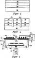
Die
Die
Mit Bezug auf
Die meisten GaN-basierten LEDs werden jedoch mit einer lateralen Topologie hergestellt. Dies liegt hauptsächlich an den Schwierigkeiten, das isolierende Substrat zu entfernen und die GaN-Waferstruktur ohne ein stützendes Substrat zu handhaben. Trotz dieser Probleme wurde das Entfernen eines isolierenden (Aufwachs-)Substrats und das nachfolgende Wafer-Bonden des resultierenden GaN-basierten Wafers auf einem Si-Substrat mit Pd/In-Metallschichten für sehr kleine Waferflächen von ungefähr 1 cm mal 1 cm nachgewiesen. Das Substrat-Entfernen und das folgende Wafer-Bonden von großflächigen Wafern bleibt aufgrund der inhomogenen Haftung zwischen dem GaN-Wafer und dem zweiten (Ersatz-)Substrat jedoch sehr schwierig. Dies ist hauptsächlich dem Verbiegen des Wafers während und nach dem Laserabheben zuzuschreiben.However, most GaN-based LEDs are manufactured with a lateral topology. This is mainly due to the difficulty of removing the insulating substrate and handling the GaN wafer structure without a supporting substrate. Despite these problems, removal of an insulating (growth) substrate and subsequent wafer bonding of the resulting GaN-based wafer to a Si substrate with Pd / In metal layers has been demonstrated for very small wafer areas of approximately 1 cm by 1 cm. However, substrate removal and subsequent wafer bonding of large area wafers remains very difficult due to inhomogeneous adhesion between the GaN wafer and the second (replacement) substrate. This is mainly due to the bending of the wafer during and after the laser lift.
Also ist ersichtlich, dass ein neues Verfahren zur Fertigung von Bauelementen mit vertikaler Topologie vorteilhaft wäre. Insbesondere wäre ein Verfahren, das für eine mechanische Stabilität der Schichten der Halbleiterwafer sorgt, die Bildung eines elektrischen Kontakts mit vertikaler Topologie ermöglicht und die Wärmeableitung verbessert, sehr nützlich, besonders bei Bauelementen, die hohen Strömen ausgesetzt sind, wie z. B. Laserdioden oder Hochleistungs-LEDs. Vorteilhafterweise würde ein solches Verfahren das Bilden mehrerer Halbleiterschichten auf einem isolierenden Substrat, das Hinzufügen einer oberen Metallträgerschicht, obere elektrische Kontakte und strukturelle Stabilität bieten, und das Entfernen des isolierenden Substrats ermöglichen. Von besonderem Nutzen wäre ein neues Verfahren zum Bilden teilgefertigter Halbleiterbauelemente auf einem Saphir-(oder anderem isolierenden)Substrat, das Hinzufügen einer oberen Metallträgerschicht auf die teilgefertigten Halbleiterschichten, das Entfernen des Saphir-(oder anderem isolierenden)Substrats, das Bilden von unteren elektrischen Kontakten und das Zerteilen der oberen Metallträgerschicht, um eine Vielzahl von Bauelementen zu erhalten. Besonders vorteilhaft wäre ein Fertigungsverfahren, das GaN-basierte LEDs mit vertikaler Topologie herstellt.Thus, it will be appreciated that a new method of manufacturing vertical topology devices would be advantageous. In particular, a method that provides for mechanical stability of the layers of semiconductor wafers, enables the formation of an electrical contact with vertical topology, and improves heat dissipation would be very useful, especially for devices exposed to high currents, such as high-current. As laser diodes or high-power LEDs. Advantageously, such a method would enable forming a plurality of semiconductor layers on an insulating substrate, adding an upper metal support layer, providing upper electrical contacts and structural stability, and removing the insulating substrate. Of particular benefit would be a novel method of forming semi-finished semiconductor devices on a sapphire (or other insulating) substrate, adding an upper metal backing layer to the partially fabricated semiconductor layers, removing the sapphire (or other insulating) substrate, forming lower electrical contacts and dicing the upper metal carrier layer to obtain a plurality of devices. Particularly advantageous would be a manufacturing process that produces GaN-based LEDs with a vertical topology.
ABRISS DER ERFINDUNGSUMMARY OF THE INVENTION
Der folgende Abriss der Erfindung wird bereitgestellt, um das Verstehen einiger der innovativen Merkmale zu erleichtern, die für die vorliegende Erfindung einmalig sind, und ist nicht als vollständige Beschreibung zu verstehen. Ein vollständiges Verständnis der verschiedenen Aspekte der Erfindung lässt sich gewinnen, indem die gesamte Beschreibung, die Ansprüche, die Zeichnungen und die Zusammenfassung zusammengenommen werden.The following summary of the invention is provided to facilitate the understanding of some of the innovative features unique to the present invention and is not to be considered as a complete description. A full understanding of the various aspects of the invention may be had by taking the entire description, claims, drawings, and abstract together.
Ein Aspekte der Erfindung betrifft eine Licht emittierende Vorrichtung, umfassend: eine leitfähige Trägerschicht; eine Elektrode ersten Typs auf der leitfähigen Trägerschicht; eine Halbleiterstruktur, die eine Halbleiterschicht ersten Typs auf der Elektrode ersten Typs, eine aktive Schicht auf der Halbleiterschicht ersten Typs und eine Halbleiterschicht zweiten Typs auf der aktiven Schicht umfasst, wobei die Elektrode ersten Type zwischen der leitfähigen Trägerschicht und der Halbleiterstruktur angeordnet ist; eine Elektrode zweiten Typs auf einer oberen Oberfläche der Halbleiterstruktur; eine Passivierungsschicht auf einer seitlichen Oberfläche und der oberen Oberfläche der Halbleiterstruktur, wobei die Passivierungsschicht auf der oberen Oberfläche der Halbleiterstruktur über der Elektrode ersten Typs angeordnet ist und die Passivierungsschicht Seitenabschnitte der Halbleiterschicht ersten Typs, der aktiven Schicht und der Halbleiterschicht zweiten Typs bedeckt; und eine Metallkontaktstelle auf der Elektrode zweiten Typs, wobei die Metallkontaktstelle mindestens ein Material aus der Gruppe Cr und Au umfasst.One aspect of the invention relates to a light-emitting device comprising: a conductive support layer; an electrode of the first type on the conductive support layer; a semiconductor structure comprising a first-type semiconductor layer on the first-type electrode, an active layer on the first-type semiconductor layer, and a second-type semiconductor layer on the active layer, the first-type electrode being interposed between the conductive support layer and the semiconductor structure; a second type electrode on an upper surface of the semiconductor structure; a passivation layer on a side surface and the top surface of the semiconductor structure, wherein the passivation layer is disposed on the top surface of the semiconductor structure over the first type electrode and the passivation layer covers side portions of the first type semiconductor layer, the active layer and the second type semiconductor layer; and a metal pad on the second type electrode, wherein the metal pad comprises at least one of Cr and Au.
In einer bevorzugten Ausführungsform umfasst die Passivierungsschicht mindestens zwei Abschnitte, die sich über Teile der Elektrode ersten Typs erstrecken. Bevorzugt ist die leitfähige Trägerschicht dicker als die Elektrode ersten Type, so dass die leitfähige Trägerschicht die Halbleiterstruktur trägt. Die leitfähige Trägerschicht kann etwa 50 μm dick und die Elektrode ersten Typs weniger als 10 nm dick sein. Ferner kann die Passivierungsschicht Siliziumdioxid oder Siliziumnitrid umfassen. Bevorzugt bedeckt die Passivierungsschicht eine Seite der Elektrode zweiten Typs. In einer besonders bevorzugten Ausführungsform umfassen die Schicht ersten Typs und die Schicht zweiten Type ein GaN-basiertes Material. Speziell kann das GaN-Material mit Silizium oder Magnesium dotiert sein. Bevorzugt umfasst die leitfähige Trägerschicht mindestens ein Material aus der Gruppe Cu, Cr, Ni, Au, Ag, Mo, Pt, Pd, W, Al und Titannitrid. Weiterhin kann die Schicht zweiten Typs dicker als die Schicht ersten Typs sein. Besonders bevorzugt umfasst die aktive Schicht InGaN/GaN. Bevorzugt ist die Passivierungsschicht teilweise auf der Elektrode zweiten Typs angeordnet. Insbesondere kann die Halbleiterschicht ersten Type vom p-Typ und die Halbleiterschicht zweiten Type vom n-Typ sein. Bevorzugt kann die die Elektrode zweiten Typs Ti/Al umfassen. Besonders bevorzugt erstreckt sich der Abschnitt der Passivierungsschicht auf der seitlichen Oberfläche der Halbleiterstruktur zum Abschnitt der Passivierungsschicht auf der oberen Oberfläche der Halbleiterstruktur. Bevorzugt umfasst die Licht emittierende Vorrichtung eine Metallschicht zwischen der Elektrode ersten Typs und der leitfähigen Trägerschicht. Beispielsweise kann die Metallschicht dazu konfiguriert sein, das Wachsen der leitfähigen Trägerschicht auf der Metallschicht zu ermöglichen. Speziell kann ein Bereich der Passivierungsschicht, der die Halbleiterschicht zweiten Typs bedeckt, größer sein als ein Bereich der Passivierungsschicht, der die Halbleiterschicht ersten Type bedeckt. Bevorzugt ist die Passivierungsschicht teilweise zwischen der Halbleiterstruktur und der leitfähigen Trägerschicht angeordnet. Ebenso kann die Passivierungsschicht auf einem Abschnitt der oberen Oberfläche der Halbleiterstruktur angeordnet sein, der nicht durch die Elektrode zweiten Typs bedeckt ist. Bevorzugt umfasst die Elektrode erster Art Pt/Au, Pd/Au, Ru/Au, Ni/Au, Cr/Au, oder ITO/Au. Weiterhin kann die leitfähige Trägerschicht eine Metallträgerschicht oder ein metallhaltiges Material umfassen. Die benachbart zu der Halbleiterschicht zweiten Typs angeordnete Passivierungsschicht kann sich bevorzugt zu einer oberen Oberfläche der leitfähigen Trägerschicht erstrecken. Bevorzugt kontaktiert die Passivierungsschicht die obere Oberfläche der Halbleiterstruktur. Ferner kann die Elektrode ersten Typs die Halbleiterstruktur kontaktieren. Hierbei ist besonders bevorzugt der Kontaktbereich zwischen der Elektrode ersten Typs und der Halbleiterstruktur größer als der Kontaktbereich zwischen der Passivierungsschicht und der oberen Oberfläche der Halbleiterstruktur.In a preferred embodiment, the passivation layer comprises at least two portions extending over portions of the first type electrode. Preferably, the conductive support layer is thicker than the first type electrode so that the conductive support layer carries the semiconductor structure. The conductive support layer may be about 50 μm thick and the first type electrode less than 10 nm thick. Furthermore, the passivation layer may comprise silicon dioxide or silicon nitride. Preferably, the passivation layer covers one side of the second type electrode. In a particularly preferred embodiment, the first type layer and the second type layer comprise a GaN-based material. Specifically, the GaN material may be doped with silicon or magnesium. Preferably, the conductive support layer comprises at least one of Cu, Cr, Ni, Au, Ag, Mo, Pt, Pd, W, Al, and titanium nitride. Furthermore, the second type layer may be thicker than the first type layer. Most preferably, the active layer comprises InGaN / GaN. Preferably, the passivation layer is partially disposed on the second type electrode. In particular, the semiconductor layer may be of the p-type first type and the n-type second type semiconductor layer. Preferably, the electrode of the second type may comprise Ti / Al. Particularly preferably, the portion of the passivation layer on the lateral surface of the semiconductor structure extends to the section the passivation layer on the upper surface of the semiconductor structure. Preferably, the light-emitting device comprises a metal layer between the first-type electrode and the conductive support layer. For example, the metal layer may be configured to facilitate growth of the conductive support layer on the metal layer. Specifically, a region of the passivation layer covering the second type semiconductor layer may be larger than a region of the passivation layer covering the first type semiconductor layer. The passivation layer is preferably arranged partially between the semiconductor structure and the conductive carrier layer. Also, the passivation layer may be disposed on a portion of the upper surface of the semiconductor structure which is not covered by the second type electrode. Preferably, the first type electrode comprises Pt / Au, Pd / Au, Ru / Au, Ni / Au, Cr / Au, or ITO / Au. Furthermore, the conductive carrier layer may comprise a metal carrier layer or a metal-containing material. The passivation layer disposed adjacent to the second-type semiconductor layer may preferably extend to an upper surface of the conductive support layer. The passivation layer preferably contacts the upper surface of the semiconductor structure. Further, the first type electrode may contact the semiconductor structure. Here, particularly preferably, the contact area between the first-type electrode and the semiconductor structure is larger than the contact area between the passivation layer and the upper surface of the semiconductor structure.
In einer besonders bevorzugten Ausführungsform der Erfindung ist die Metallkontaktstelle höher angeordnet als die Passivierungsschicht auf der oberen Oberfläche der Halbleiterstruktur. Bevorzugt kann sich ferner die Metallkontaktstelle über Teile der Passivierungsschicht erstrecken.In a particularly preferred embodiment of the invention, the metal pad is arranged higher than the passivation layer on the upper surface of the semiconductor structure. Furthermore, the metal contact point may preferably extend over parts of the passivation layer.
Die neuen Merkmale der vorliegenden Erfindung werden nach Prüfung der folgenden detaillierten Beschreibung der Erfindung für den Fachmann ersichtlich werden oder können durch Ausführen der vorliegenden Erfindung erlernt werden. Es sollte jedoch verstanden werden, dass die detaillierte Beschreibung der Erfindung und die speziellen dargestellten Beispiele nur zur Veranschaulichung bereitgestellt werden, während sie bestimmte Ausführungsformen der vorliegenden Erfindung aufzeigen, weil verschiedene Änderungen und Modifikationen im Umfang der Erfindung dem Fachmann aus der detaillierten Beschreibung der Erfindung und den folgenden Ansprüchen ersichtlich werden.The novel features of the present invention will become apparent to those skilled in the art upon examination of the following detailed description of the invention, or may be learned by practice of the present invention. It should be understood, however, that the detailed description of the invention and the specific examples illustrated are provided by way of illustration only, showing certain embodiments of the present invention, as various changes and modifications within the scope of the invention will become apparent to those skilled in the art from the detailed description of the invention the following claims.
KURZE BESCHREIBUNG DER ZEICHNUNGENBRIEF DESCRIPTION OF THE DRAWINGS
Die begleitenden Figuren, in denen sich Referenznummern in allen separaten Ansichten auf identische oder funktionell ähnliche Elemente beziehen und die in die Beschreibung eingebunden sind und einen Teil derselben bilden, dienen zusammen mit der detaillierten Beschreibung der Erfindung zur Erläuterung der Prinzipien der vorliegenden Erfindung.The accompanying drawings, in which reference numbers in all separate views refer to identical or functionally similar elements, and which are incorporated in and form a part of the specification, together with the detailed description of the invention, serve to explain the principles of the present invention.
In den Zeichnungen:In the drawings:
die
DETAILLIERTE BESCHREIBUNG DER VERANSCHAULICHTEN AUSFÜHRUNGSFORMENDETAILED DESCRIPTION OF THE ILLUSTRATED EMBODIMENTS
Die Prinzipien der vorliegenden Erfindung stellen Halbleiterbauelemente und Verfahren zur Fertigung derselben bereit, wie z. B. von GaN-basierten LEDs mit vertikaler Topologie auf isolierenden Susbtraten, wie z. B. Saphirsubstraten, mit Hilfe von Metallträgerschichten. Während diese Prinzipien in der detaillierten Beschreibung eines Verfahrens zur Fertigung GaN-basierter LEDs mit vertikaler Topologie auf einem Saphirsubstrat veranschaulicht werden, reichen die Prinzipien selbst weiter als das veranschaulichte Verfahren. Daher dürfen die Prinzipien der vorliegenden Erfindung nur durch die angehängten Ansprüche begrenzt werden.The principles of the present invention provide semiconductor devices and methods for fabricating the same, such as, for example, US Pat. B. of GaN-based LEDs with vertical topology on insulating Susbtraten such. B. sapphire substrates, with the aid of metal carrier layers. While these principles are illustrated in the detailed description of a method of fabricating GaN-based vertical topology LEDs on a sapphire substrate, the principles themselves extend farther than the illustrated method. Therefore, the principles of the present invention should be limited only by the appended claims.
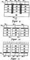
Die
Mit Bezug auf
Noch immer mit Bezug auf
Mit Bezug auf
Aufgrund der Härte von Saphir und GaN sind die Gräben
Im veranschaulichten Beispiel ist der Fotolack vorteilhafterweise auf eine Dicke von etwa 10 μm rotationsbeschichtet. Im Allgemeinen sollte die Fotolackdicke jedoch etwa gleich der Dicke der GaN-basierten LED-Schichtstruktur mit vertikaler Topologie plus der Ätztiefe in das Saphirsubstrat
Nach dem Festlegen der Ritzlinien wird die Struktur von
Noch mit Bezug auf
Mit Bezug nun auf
Wie in
Mit Bezug auf
Jetzt zu
Die Laserabhebeprozesse werden im
Immer noch mit Bezug auf
Jetzt zu
Jetzt zu
Jetzt zu
Jetzt zu
Nachdem die Metallkontaktstellen
Vorstehend wurde das Bilden von Gräben
Die Prinzipien der vorliegenden Erfindung liefern somit Halbleiterbauelemente auf isolierenden Substraten, wobei zur Herstellung derselben zunächst Halbleiterschichten auf dem isolierenden Substrat gebildet werden, anschließend eine Metallschicht über den Halbleiterschichten gebildet wird und anschließend das isolierende Substrat entfernt wird, um einen strukturell gestützten Wafer zu isolieren, welcher die gebildeten Halbleiterschichten und die Metallschicht beinhaltet. Die Metallschicht trägt die Halbleiterschichten, um ein Verziehen (Warping) und/oder eine andere Beschädigung zu vermeiden, und stellt elektrische Kontakte bereit. Vorteilhafterweise beinhaltet die Metallschicht ein Metall, wie z. B. Cu, Cr, Ni, Au, Ag, Mo, Pt, Pd, W oder Al, oder ein metallhaltiges Material, wie z. B. Titannitrid. Die Metallschicht kann auf vielerlei Weise gebildet werden, z. B. durch galvanische Beschichtung, durch nicht-galvanische Beschichtung, durch CVD-Beschichtung oder durch Sputtern. Anschließend können den Halbleiterschichten untere elektrische Kontakte hinzugefügt und danach einzelne Halbleiterbauelemente aus der resultierenden Struktur getrennt werden.The principles of the present invention thus provide semiconductor devices on insulating substrates, wherein semiconductor layers are first formed on the insulating substrate to produce them, then a metal layer is formed over the semiconductor layers, and then the insulating substrate is removed to insulate a structurally-supported wafer includes the formed semiconductor layers and the metal layer. The metal layer carries the semiconductor layers to prevent warping and / or other damage and provides electrical contacts. Advantageously, the metal layer includes a metal, such as. As Cu, Cr, Ni, Au, Ag, Mo, Pt, Pd, W or Al, or a metal-containing material such. B. titanium nitride. The metal layer can be formed in many ways, e.g. As by electroplating, by non-galvanic coating, by CVD coating or by sputtering. Subsequently, lower electrical contacts may be added to the semiconductor layers and then individual semiconductor devices may be separated from the resulting structure.
Die Prinzipien der vorliegenden Erfindung stellen des Weiteren GaN-basierte Bauelemente mit vertikaler Topologie auf einem isolierenden Substrat bereit, wobei die Herstellung derselben die Verwendung einer Metallträgerschicht und das nachfolgende Entfernen des isolierenden Substrats umfasst. Gemäß diesem Verfahren werden Halbleiterschichten für die GaN-basierten Bauelemente mit normalen Halbleiterfertigungstechniken auf einem isolierenden Substrat (aus Saphir) gebildet. Anschließend werden Gräben durch die Halbleiterschichten gebildet, welche die Grenzen der einzelnen Bauelemente festlegen. Diese Gräben können auch in das isolierende Substrat hinein gebildet werden. Die Gräben werden vorteilhafterweise durch reaktives Ionenätzen mit induktiv gekoppeltem Plasma (Inductive Coupled Plasma Reactive Ion Etching/ICPRIE) ausgebildet. Anschließend werden die Gräben mit einer leicht zu entfernenden Schicht (wie z. B. einem Fotolack) gefüllt. Sodann wird auf den Halbleiterschichten eine Metallträgerstruktur gebildet. Vorteilhafterweise beinhaltet die Metallträgerstruktur ein Metall, wie z. B. Cu, Cr, Ni, Au, Ag, Mo, Pt, Pd, W oder Al, oder ein metallhaltiges Material, wie z. B. Titannitrid. Die Metallträgerstruktur kann auf vielerlei Weise gebildet werden, z. B. durch galvanische Beschichtung, durch nicht-galvanische Beschichtung, durch CVD-Beschichtung oder durch Sputtern. Danach wird das isolierende Substrat entfernt, vorteilhafterweise mit einem Laserabhebeprozess. Anschließend werden den einzelnen Bauelementen elektrische Kontakte, eine Passivierungsschicht und metallische Kontaktstellen hinzugefügt und die einzelnen Bauelemente dann singuliert.The principles of the present invention further provide GaN-based devices with a vertical topology on an insulating substrate, the fabrication of which comprises the use of a metal carrier layer and the subsequent removal of the insulating substrate. According to this method, semiconductor layers for the GaN-based devices are formed on an insulating substrate (sapphire) with ordinary semiconductor fabrication techniques. Subsequently, trenches are formed by the semiconductor layers, which define the boundaries of the individual components. These trenches can also be formed into the insulating substrate. The trenches are advantageously formed by Inductive Coupled Plasma Reactive Ion Etching (ICPRIE) reactive ion etching. Subsequently, the trenches are filled with an easily removable layer (such as a photoresist). Then, a metal support structure is formed on the semiconductor layers. Advantageously, the metal support structure includes a metal, such as. As Cu, Cr, Ni, Au, Ag, Mo, Pt, Pd, W or Al, or a metal-containing material such. B. titanium nitride. The metal support structure can be formed in many ways, e.g. As by electroplating, by non-galvanic coating, by CVD coating or by sputtering. Thereafter, the insulating substrate is removed, advantageously with a laser lift-off process. Subsequently, the individual components electrical contacts, a passivation layer and metallic contact points are added and the individual components then singulated.
Die Prinzipien der vorliegenden Erfindung stellen speziell GaN-basierte LEDs mit vertikaler Topologie auf Saphirsubstraten bereit. Hierzu werden Halbleiterschichten für die GaN-basierten LEDs mit vertikaler Topologie mit normalen Halbleiterfertigungstechniken auf einem Saphirsubstrat gebildet. Anschließend werden Gräben durch die Halbleiterschichten gebildet, welche die Grenzen der einzelnen GaN-basierten LEDs mit vertikaler Topologie festlegen. Diese Gräben können auch in das Saphirsubstrat hinein gebildet werden. Die Gräben werden vorteilhafterweise durch reaktives Ionenätzen mit induktiv gekoppeltem Plasma (Inductive Coupled Plasma Reactive Ion Etching/ICPRIE) ausgebildet. Vorteilhafterweise werden die Gräben mit ICPRIE hergestellt. Anschließend werden die Gräben vorteilhafterweise mit einer leicht zu entfernenden Schicht (wie z. B. einem Fotolack) gefüllt. Sodann wird auf den Halbleiterschichten eine Metallträgerstruktur gebildet. Vorteilhafterweise beinhaltet die Metallträgerstruktur ein Metall, wie z. B. Cu, Cr, Ni, Au, Ag, Mo, Pt, Pd, W oder Al, oder ein metallhaltiges Material, wie z. B. Titannitrid. Die Metallschicht kann auf vielerlei Weise gebildet werden, z. B. durch galvanische Beschichtung, nicht-galvanische Beschichtung, CVD-Beschichtung oder Sputtern. Danach wird das isolierende Substrat entfernt, vorteilhafterweise mit einem Laserabhebeprozess. Anschließend werden den einzelnen Bauelementen elektrische Kontakte, eine Passivierungsschicht und metallische Kontaktstellen hinzugefügt. Danach werden die einzelnen Elemente singuliert.The principles of the present invention specifically provide GaN based vertical topology LEDs on sapphire substrates. For this purpose, semiconductor layers for the vertical topology GaN based LEDs are formed on a sapphire substrate using standard semiconductor fabrication techniques. Subsequently, trenches are formed through the semiconductor layers which define the boundaries of the individual GaN-based vertical topology LEDs. These trenches can also be formed into the sapphire substrate. The trenches are advantageously formed by Inductive Coupled Plasma Reactive Ion Etching (ICPRIE) reactive ion etching. Advantageously, the trenches are made with ICPRIE. Subsequently, the trenches are advantageously filled with an easily removable layer (such as a photoresist). Then, a metal support structure is formed on the semiconductor layers. Advantageously, the metal support structure includes a metal, such as. As Cu, Cr, Ni, Au, Ag, Mo, Pt, Pd, W or Al, or a metal-containing material such. B. titanium nitride. The metal layer can be formed in many ways, e.g. As by electroplating, non-galvanic coating, CVD coating or sputtering. Thereafter, the insulating substrate is removed, advantageously with a laser lift-off process. Subsequently, the individual components electrical contacts, a passivation layer and metallic contact points are added. Then the individual elements are singulated.
Die hierin dargestellten Ausführungsformen und Beispiele werden aufgeführt, um die vorliegende Erfindung und ihre praktische Anwendung bestmöglich zu erläutern und dadurch dem Fachmann zu ermöglichen, die Erfindung anzuwenden und zu nutzen. Der Fachmann wird jedoch erkennen, dass die vorstehende Beschreibung und die Beispiele nur zum Zwecke der Veranschaulichung und Beispielnennung gegeben wurden. Andere Variationen und Änderungen der vorliegenden Erfindung werden für den Fachmann ersichtlich sein, und es ist die Absicht der beigefügten Ansprüche, solche Variationen und Änderungen abzudecken. Die hier gegebene Beschreibung ist nicht als erschöpfend oder den Umfang der Erfindung eingrenzend gedacht. Viele Änderungen und Variationen sind im Lichte der obigen Lehre möglich, ohne dabei vom Geist und Umfang der folgenden Ansprüche abzuweichen. Es ist vorgesehen, dass die Nutzung der vorliegenden Erfindung Komponenten mit unterschiedlichen Eigenschaften beinhalten kann. Es ist beabsichtigt, dass der Umfang der vorliegenden Erfindung von den hierzu beigefügten Ansprüchen festgelegt wird. Diese Ansprüche nehmen die Äquivalente in jeder Hinsicht vollständig zur Kenntnis.The embodiments and examples presented herein are set forth in order to best explain the present invention and its practical application, thereby enabling those skilled in the art to practice and use the invention. However, those skilled in the art will recognize that the foregoing description and examples have been presented for purposes of illustration and example only. Other variations and changes of the present invention will be apparent to those skilled in the art, and it is the intent of the appended claims to cover such variations and changes. The description given herein is not intended to be exhaustive or limited to the scope of the invention. Many changes and variations are possible in light of the above teachings without departing from the spirit and scope of the following claims. It is contemplated that use of the present invention may include components having different characteristics. It is intended that the scope of the present invention be limited to those of this attached claims. These claims fully acknowledge the equivalents in all respects.
ZITATE ENTHALTEN IN DER BESCHREIBUNG QUOTES INCLUDE IN THE DESCRIPTION
Diese Liste der vom Anmelder aufgeführten Dokumente wurde automatisiert erzeugt und ist ausschließlich zur besseren Information des Lesers aufgenommen. Die Liste ist nicht Bestandteil der deutschen Patent- bzw. Gebrauchsmusteranmeldung. Das DPMA übernimmt keinerlei Haftung für etwaige Fehler oder Auslassungen.This list of the documents listed by the applicant has been generated automatically and is included solely for the better information of the reader. The list is not part of the German patent or utility model application. The DPMA assumes no liability for any errors or omissions.
Zitierte PatentliteraturCited patent literature
- US 6071795[0041]US 6071795[0041]
Zitierte Nicht-PatentliteraturCited non-patent literature
- Kelly u. a. „Optical process for lift-oft of group III-nitride films”, Physica Status Solidi (a), Band 159, 1997, Seiten R3–R4[0041]Kelly et al. "Optical process for lift-often of group III nitride films", Physica Status Solidi (a), Vol. 159, 1997, pages R3-R4[0041]
Claims (26)
Translated fromGermanApplications Claiming Priority (2)
| Application Number | Priority Date | Filing Date | Title |
|---|---|---|---|
| US10/118,316US20030189215A1 (en) | 2002-04-09 | 2002-04-09 | Method of fabricating vertical structure leds |
| US10/118,316 | 2002-04-09 |
Publications (1)
| Publication Number | Publication Date |
|---|---|
| DE20321881U1true DE20321881U1 (en) | 2011-11-30 |
Family
ID=28674400
Family Applications (3)
| Application Number | Title | Priority Date | Filing Date |
|---|---|---|---|
| DE20321881UExpired - LifetimeDE20321881U1 (en) | 2002-04-09 | 2003-03-31 | LEDS with vertical structure |
| DE60324413TExpired - LifetimeDE60324413D1 (en) | 2002-04-09 | 2003-03-31 | METHOD FOR PRODUCING VERTICAL STRUCTURES LEDS |
| DE20321880UExpired - LifetimeDE20321880U1 (en) | 2002-04-09 | 2003-03-31 | LEDS with vertical structure |
Family Applications After (2)
| Application Number | Title | Priority Date | Filing Date |
|---|---|---|---|
| DE60324413TExpired - LifetimeDE60324413D1 (en) | 2002-04-09 | 2003-03-31 | METHOD FOR PRODUCING VERTICAL STRUCTURES LEDS |
| DE20321880UExpired - LifetimeDE20321880U1 (en) | 2002-04-09 | 2003-03-31 | LEDS with vertical structure |
Country Status (8)
| Country | Link |
|---|---|
| US (19) | US20030189215A1 (en) |
| EP (8) | EP2863444B1 (en) |
| JP (5) | JP5325365B2 (en) |
| KR (1) | KR100921457B1 (en) |
| AT (1) | ATE412972T1 (en) |
| AU (1) | AU2003241280A1 (en) |
| DE (3) | DE20321881U1 (en) |
| WO (1) | WO2003088318A2 (en) |
Families Citing this family (289)
| Publication number | Priority date | Publication date | Assignee | Title |
|---|---|---|---|---|
| US7067849B2 (en) | 2001-07-17 | 2006-06-27 | Lg Electronics Inc. | Diode having high brightness and method thereof |
| JPWO2003034508A1 (en)* | 2001-10-12 | 2005-02-03 | 日亜化学工業株式会社 | Light emitting device and manufacturing method thereof |
| US6949395B2 (en) | 2001-10-22 | 2005-09-27 | Oriol, Inc. | Method of making diode having reflective layer |
| US7148520B2 (en) | 2001-10-26 | 2006-12-12 | Lg Electronics Inc. | Diode having vertical structure and method of manufacturing the same |
| US20030189215A1 (en) | 2002-04-09 | 2003-10-09 | Jong-Lam Lee | Method of fabricating vertical structure leds |
| US8294172B2 (en)* | 2002-04-09 | 2012-10-23 | Lg Electronics Inc. | Method of fabricating vertical devices using a metal support film |
| US20040140474A1 (en)* | 2002-06-25 | 2004-07-22 | Matsushita Electric Industrial Co., Ltd. | Semiconductor light-emitting device, method for fabricating the same and method for bonding the same |
| US6841802B2 (en) | 2002-06-26 | 2005-01-11 | Oriol, Inc. | Thin film light emitting diode |
| KR101030068B1 (en)* | 2002-07-08 | 2011-04-19 | 니치아 카가쿠 고교 가부시키가이샤 | Nitride semiconductor device manufacturing method and nitride semiconductor device |
| DE10245631B4 (en)* | 2002-09-30 | 2022-01-20 | OSRAM Opto Semiconductors Gesellschaft mit beschränkter Haftung | semiconductor device |
| US20050082575A1 (en)* | 2002-10-29 | 2005-04-21 | Lung-Chien Chen | Structure and manufacturing method for GaN light emitting diodes |
| US7244628B2 (en)* | 2003-05-22 | 2007-07-17 | Matsushita Electric Industrial Co., Ltd. | Method for fabricating semiconductor devices |
| JP5142523B2 (en)* | 2003-06-04 | 2013-02-13 | チェオル ユー,ミュング | Vertical structure composite semiconductor device |
| DE10326507A1 (en)* | 2003-06-12 | 2005-01-13 | Infineon Technologies Ag | A method of making a fracture resistant disc shaped article and associated semiconductor circuit assembly |
| US8999736B2 (en)* | 2003-07-04 | 2015-04-07 | Epistar Corporation | Optoelectronic system |
| US7915085B2 (en) | 2003-09-18 | 2011-03-29 | Cree, Inc. | Molded chip fabrication method |
| US20080210970A1 (en)* | 2003-09-19 | 2008-09-04 | Tinggi Technologies Private Limited | Fabrication of Conductive Metal Layer on Semiconductor Devices |
| JP2007521635A (en)* | 2003-09-19 | 2007-08-02 | ティンギ テクノロジーズ プライベート リミテッド | Semiconductor device manufacturing |
| TWM255514U (en)* | 2003-10-16 | 2005-01-11 | Arima Optoelectronics Corp | Structure improvement of Gallium Indium Nitride light-emitting diode |
| KR100576854B1 (en)* | 2003-12-20 | 2006-05-10 | 삼성전기주식회사 | Nitride semiconductor manufacturing method and nitride semiconductor using same |
| KR100576856B1 (en)* | 2003-12-23 | 2006-05-10 | 삼성전기주식회사 | Nitride semiconductor light emitting device and manufacturing method |
| US6969626B2 (en)* | 2004-02-05 | 2005-11-29 | Advanced Epitaxy Technology | Method for forming LED by a substrate removal process |
| JP2005223165A (en) | 2004-02-06 | 2005-08-18 | Sanyo Electric Co Ltd | Nitride-based light emitting device |
| KR20070013273A (en)* | 2004-03-15 | 2007-01-30 | 팅기 테크놀러지스 프라이빗 리미티드 | Fabrication of Semiconductor Devices |
| US7122398B1 (en)* | 2004-03-25 | 2006-10-17 | Nanosolar, Inc. | Manufacturing of optoelectronic devices |
| JP2005298554A (en)* | 2004-04-07 | 2005-10-27 | Sumitomo Electric Ind Ltd | Stretched polytetrafluoroethylene porous membrane having elastic recovery in the film thickness direction, production method thereof, and use of the porous membrane |
| EP1756875A4 (en)* | 2004-04-07 | 2010-12-29 | Tinggi Technologies Private Ltd | FABRICATION OF A RETROFLECTIVE LAYER ON SEMICONDUCTOR ELECTROLUMINESCENT DIODES |
| EP1749308A4 (en)* | 2004-04-28 | 2011-12-28 | Verticle Inc | SEMICONDUCTOR DEVICES WITH VERTICAL STRUCTURE |
| KR100595884B1 (en)* | 2004-05-18 | 2006-07-03 | 엘지전자 주식회사 | Nitride semiconductor device manufacturing method |
| TWI433343B (en)* | 2004-06-22 | 2014-04-01 | Verticle Inc | Vertical structure semiconductor device with improved light output |
| JP4841550B2 (en) | 2004-06-30 | 2011-12-21 | ソウル オプト デバイス カンパニー リミテッド | LIGHT EMITTING ELEMENT, ITS MANUFACTURING METHOD, AND LIGHT EMITTING DEVICE USING THE SAME |
| TWM261838U (en)* | 2004-09-16 | 2005-04-11 | Super Nova Optoelectronics Cor | Structure for GaN based LED with high light extraction efficiency |
| US20060076574A1 (en)* | 2004-10-12 | 2006-04-13 | Liang-Wen Wu | Gallium-nitride based light-emitting diodes structure with high reverse withstanding voltage and anti-ESD capability |
| JP4999696B2 (en)* | 2004-10-22 | 2012-08-15 | ソウル オプト デバイス カンパニー リミテッド | GaN-based compound semiconductor light emitting device and manufacturing method thereof |
| KR100667508B1 (en) | 2004-11-08 | 2007-01-10 | 엘지전자 주식회사 | Light emitting device and manufacturing method thereof |
| TWI389334B (en)* | 2004-11-15 | 2013-03-11 | Verticle Inc | Method of manufacturing and separating semiconductor devices |
| US20060124941A1 (en)* | 2004-12-13 | 2006-06-15 | Lee Jae S | Thin gallium nitride light emitting diode device |
| US8802465B2 (en) | 2005-01-11 | 2014-08-12 | SemiLEDs Optoelectronics Co., Ltd. | Method for handling a semiconductor wafer assembly |
| US20060154393A1 (en)* | 2005-01-11 | 2006-07-13 | Doan Trung T | Systems and methods for removing operating heat from a light emitting diode |
| US8318519B2 (en)* | 2005-01-11 | 2012-11-27 | SemiLEDs Optoelectronics Co., Ltd. | Method for handling a semiconductor wafer assembly |
| US7432119B2 (en)* | 2005-01-11 | 2008-10-07 | Semileds Corporation | Light emitting diode with conducting metal substrate |
| US7186580B2 (en) | 2005-01-11 | 2007-03-06 | Semileds Corporation | Light emitting diodes (LEDs) with improved light extraction by roughening |
| US8871547B2 (en) | 2005-01-11 | 2014-10-28 | SemiLEDs Optoelectronics Co., Ltd. | Method for fabricating vertical light emitting diode (VLED) structure using a laser pulse to remove a carrier substrate |
| EP1681712A1 (en)* | 2005-01-13 | 2006-07-19 | S.O.I. Tec Silicon on Insulator Technologies S.A. | Method of producing substrates for optoelectronic applications |
| CN100352116C (en)* | 2005-01-18 | 2007-11-28 | 北京大学 | Preparation method of GaN-based laser diode with naturally cleaved cavity surface |
| TWI308396B (en)* | 2005-01-21 | 2009-04-01 | Epistar Corp | Light emitting diode and fabricating method thereof |
| KR101165257B1 (en)* | 2005-01-26 | 2012-07-19 | 서울옵토디바이스주식회사 | Luminescence device and method of manufacturing the same |
| US7932111B2 (en)* | 2005-02-23 | 2011-04-26 | Cree, Inc. | Substrate removal process for high light extraction LEDs |
| JP4818732B2 (en)* | 2005-03-18 | 2011-11-16 | シャープ株式会社 | Method of manufacturing nitride semiconductor device |
| KR100638732B1 (en)* | 2005-04-15 | 2006-10-30 | 삼성전기주식회사 | Manufacturing method of vertical structure nitride semiconductor light emitting device |
| JP4707450B2 (en)* | 2005-05-18 | 2011-06-22 | イーストマン コダック カンパニー | Image processing apparatus and white balance adjustment apparatus |
| KR101128612B1 (en)* | 2005-05-24 | 2012-03-26 | 엘지이노텍 주식회사 | Light emitting device and method for fabricating the same |
| US7625778B2 (en)* | 2005-06-08 | 2009-12-01 | Chunghwa Picture Tubes, Ltd. | Method of manufacturing a substrate-free flip chip light emitting diode |
| US8168000B2 (en)* | 2005-06-15 | 2012-05-01 | International Rectifier Corporation | III-nitride semiconductor device fabrication |
| KR20060131327A (en)* | 2005-06-16 | 2006-12-20 | 엘지전자 주식회사 | Manufacturing method of light emitting diode |
| KR100599012B1 (en)* | 2005-06-29 | 2006-07-12 | 서울옵토디바이스주식회사 | Light Emitting Diode Having Thermally Conductive Substrate And Method Of Manufacturing The Same |
| KR100849788B1 (en)* | 2005-06-30 | 2008-07-31 | 삼성전기주식회사 | Manufacturing method of vertical light emitting device |
| KR100658303B1 (en)* | 2005-07-04 | 2006-12-14 | 엘지전자 주식회사 | Light Emitting Diode of Vertical Structure Including Metal Support Layer |
| KR100606551B1 (en)* | 2005-07-05 | 2006-08-01 | 엘지전자 주식회사 | Method of manufacturing light emitting device |
| KR100691186B1 (en)* | 2005-07-12 | 2007-03-09 | 삼성전기주식회사 | Manufacturing method of vertical structure light emitting diode |
| KR100617873B1 (en)* | 2005-07-15 | 2006-08-28 | 엘지전자 주식회사 | Vertical Light Emitting Diode and Manufacturing Method Thereof |
| KR100682271B1 (en)* | 2005-07-29 | 2007-02-15 | 엘지전자 주식회사 | Vertical light emitting device manufacturing method |
| KR100691111B1 (en)* | 2005-08-09 | 2007-03-09 | 엘지전자 주식회사 | Vertical Light Emitting Diode and Manufacturing Method Thereof |
| KR100975711B1 (en)* | 2005-09-13 | 2010-08-12 | 쇼와 덴코 가부시키가이샤 | Nitride semiconductor light emitting device and manufacturing method thereof |
| JP4799975B2 (en)* | 2005-09-16 | 2011-10-26 | 昭和電工株式会社 | Nitride-based semiconductor light-emitting device and manufacturing method thereof |
| JP2007081312A (en)* | 2005-09-16 | 2007-03-29 | Showa Denko Kk | Method of manufacturing nitride-based semiconductor light-emitting element |
| EP1925039A4 (en)* | 2005-09-16 | 2012-07-04 | Showa Denko Kk | METHOD FOR MANUFACTURING A NITRIDE SEMICONDUCTOR LIGHT DEVICE |
| JP4799974B2 (en)* | 2005-09-16 | 2011-10-26 | 昭和電工株式会社 | Nitride-based semiconductor light-emitting device and manufacturing method thereof |
| KR100691363B1 (en)* | 2005-09-23 | 2007-03-12 | 삼성전기주식회사 | Manufacturing method of vertical structure light emitting diode |
| SG130975A1 (en)* | 2005-09-29 | 2007-04-26 | Tinggi Tech Private Ltd | Fabrication of semiconductor devices for light emission |
| DE102005061346A1 (en)* | 2005-09-30 | 2007-04-05 | Osram Opto Semiconductors Gmbh | Optoelectronic semiconductor chip and production process has thin-film semiconductor body with radiation-producing active region and a mechanically stable carrier layer on the semiconductor body |
| DE102005053274A1 (en)* | 2005-09-30 | 2007-04-12 | Osram Opto Semiconductors Gmbh | Making semiconductor chips involves building up semiconductor layers, applying metal plating to epitaxial growth substrate and depositing metal layer galvanically before structuring and separating layers into individual chips |
| KR100714589B1 (en)* | 2005-10-05 | 2007-05-07 | 삼성전기주식회사 | Manufacturing method of vertical structure light emitting diode |
| KR100657735B1 (en)* | 2005-10-11 | 2006-12-14 | 엘지전자 주식회사 | Vertical light emitting device manufacturing method |
| US7723718B1 (en)* | 2005-10-11 | 2010-05-25 | SemiLEDs Optoelectronics Co., Ltd. | Epitaxial structure for metal devices |
| US8778780B1 (en)* | 2005-10-13 | 2014-07-15 | SemiLEDs Optoelectronics Co., Ltd. | Method for defining semiconductor devices |
| SG131803A1 (en) | 2005-10-19 | 2007-05-28 | Tinggi Tech Private Ltd | Fabrication of transistors |
| KR100752348B1 (en)* | 2005-10-20 | 2007-08-27 | (주) 비앤피 사이언스 | Vertical structure light emitting diode manufacturing method |
| MY148126A (en)* | 2005-10-21 | 2013-02-28 | Taylor Biomass Energy Llc | Process and system for gasification with in-situ tar removal |
| WO2007050736A2 (en)* | 2005-10-26 | 2007-05-03 | Velox Semiconductor Corporation | Vertical structure semiconductor devices and method of fabricating the same |
| CN100474642C (en)* | 2005-10-27 | 2009-04-01 | 晶能光电(江西)有限公司 | Indium gallium aluminium nitrogen semi-conductor luminous element containing metallic chromium substrate and manufacturing method thereof |
| US7829909B2 (en)* | 2005-11-15 | 2010-11-09 | Verticle, Inc. | Light emitting diodes and fabrication methods thereof |
| JP2007158111A (en)* | 2005-12-06 | 2007-06-21 | Toyoda Gosei Co Ltd | Manufacturing method of semiconductor device |
| SG133432A1 (en)* | 2005-12-20 | 2007-07-30 | Tinggi Tech Private Ltd | Localized annealing during semiconductor device fabrication |
| KR100764420B1 (en)* | 2005-12-23 | 2007-10-05 | 삼성전기주식회사 | Slim LED Package |
| JP2007207981A (en)* | 2006-02-01 | 2007-08-16 | Rohm Co Ltd | Method of manufacturing nitride semiconductor light-emitting device |
| KR100735488B1 (en)* | 2006-02-03 | 2007-07-04 | 삼성전기주식회사 | Method of manufacturing gallium nitride-based light emitting diode device |
| KR100714637B1 (en)* | 2006-02-09 | 2007-05-07 | 삼성전기주식회사 | Manufacturing method of vertical structure light emitting diode |
| KR101125339B1 (en) | 2006-02-14 | 2012-03-27 | 엘지이노텍 주식회사 | Nitride compound based light-emitting semiconductor and fabricating method thereof |
| US7928462B2 (en) | 2006-02-16 | 2011-04-19 | Lg Electronics Inc. | Light emitting device having vertical structure, package thereof and method for manufacturing the same |
| US8124957B2 (en) | 2006-02-22 | 2012-02-28 | Cree, Inc. | Low resistance tunnel junctions in wide band gap materials and method of making same |
| US7737451B2 (en)* | 2006-02-23 | 2010-06-15 | Cree, Inc. | High efficiency LED with tunnel junction layer |
| JP2007258338A (en)* | 2006-03-22 | 2007-10-04 | Rohm Co Ltd | Semiconductor light-emitting element |
| US7696523B2 (en) | 2006-03-14 | 2010-04-13 | Lg Electronics Inc. | Light emitting device having vertical structure and method for manufacturing the same |
| KR100774196B1 (en)* | 2006-03-14 | 2007-11-08 | 엘지전자 주식회사 | Vertical light emitting device manufacturing method |
| US8420505B2 (en)* | 2006-03-25 | 2013-04-16 | International Rectifier Corporation | Process for manufacture of thin wafer |
| JP5232971B2 (en)* | 2006-04-28 | 2013-07-10 | 豊田合成株式会社 | Method for manufacturing nitride-based semiconductor light-emitting device |
| DE102006033502A1 (en)* | 2006-05-03 | 2007-11-15 | Osram Opto Semiconductors Gmbh | Radiation-emitting semiconductor body with carrier substrate and method for producing such |
| KR100736623B1 (en)* | 2006-05-08 | 2007-07-09 | 엘지전자 주식회사 | Vertical light emitting device and manufacturing method |
| KR100735496B1 (en)* | 2006-05-10 | 2007-07-04 | 삼성전기주식회사 | Method for manufacturing vertical structure gallium nitride based LED device |
| KR101113878B1 (en)* | 2006-06-23 | 2012-03-09 | 엘지이노텍 주식회사 | Light emitting diode having vertical topology and method of making the same |
| SG140473A1 (en) | 2006-08-16 | 2008-03-28 | Tinggi Tech Private Ltd | Improvements in external light efficiency of light emitting diodes |
| US20080054291A1 (en)* | 2006-08-31 | 2008-03-06 | Samsung Electronics Co., Ltd. | Vertical semiconductor light-emitting device and method of manufacturing the same |
| SG140512A1 (en)* | 2006-09-04 | 2008-03-28 | Tinggi Tech Private Ltd | Electrical current distribution in light emitting devices |
| KR101239850B1 (en)* | 2006-09-26 | 2013-03-06 | 서울옵토디바이스주식회사 | Vertical light emitting diode and method of fabricating the same |
| KR100786802B1 (en)* | 2006-09-26 | 2007-12-18 | 한국광기술원 | Vertical semiconductor light emitting device having a protective film and manufacturing method |
| US8921204B2 (en)* | 2006-10-11 | 2014-12-30 | SemiLEDs Optoelectronics Co., Ltd. | Method for fabricating semiconductor dice by separating a substrate from semiconductor structures using multiple laser pulses |
| US20080087875A1 (en)* | 2006-10-11 | 2008-04-17 | Feng-Hsu Fan | Protection for the epitaxial structure of metal devices |
| US20080089829A1 (en)* | 2006-10-13 | 2008-04-17 | Rensselaer Polytechnic Institute | In-situ back-contact formation and site-selective assembly of highly aligned carbon nanotubes |
| KR101252558B1 (en)* | 2006-11-06 | 2013-04-08 | 엘지이노텍 주식회사 | Method for making LED having vertical topology |
| KR100867541B1 (en)* | 2006-11-14 | 2008-11-06 | 삼성전기주식회사 | Manufacturing method of vertical light emitting device |
| JP4910664B2 (en)* | 2006-11-30 | 2012-04-04 | 豊田合成株式会社 | Method for manufacturing group III-V semiconductor device |
| US7781241B2 (en) | 2006-11-30 | 2010-08-24 | Toyoda Gosei Co., Ltd. | Group III-V semiconductor device and method for producing the same |
| TWI410164B (en)* | 2007-02-12 | 2013-09-21 | Nat Univ Chung Hsing | Light strip of solid state light emitting element |
| US20080217634A1 (en)* | 2007-03-06 | 2008-09-11 | Wen-Huang Liu | Vertical light-emitting diode structure with omni-directional reflector |
| JP4290745B2 (en) | 2007-03-16 | 2009-07-08 | 豊田合成株式会社 | Method for manufacturing group III-V semiconductor device |
| KR100888966B1 (en)* | 2007-03-20 | 2009-03-17 | 엘지전자 주식회사 | Manufacturing method of vertical light emitting device |
| KR100871742B1 (en)* | 2007-05-25 | 2008-12-05 | 김구영 | Multiple control device of light emitting diode |
| KR100858322B1 (en)* | 2007-05-30 | 2008-09-11 | (주)웨이브스퀘어 | Method for manufacturing gallium nitride based LED device having vertical structure |
| US7646025B1 (en) | 2007-05-31 | 2010-01-12 | Chien-Min Sung | Diamond LED devices and associated methods |
| US8309967B2 (en)* | 2007-05-31 | 2012-11-13 | Chien-Min Sung | Diamond LED devices and associated methods |
| US9082892B2 (en)* | 2007-06-11 | 2015-07-14 | Manulius IP, Inc. | GaN Based LED having reduced thickness and method for making the same |
| TWI411124B (en)* | 2007-07-10 | 2013-10-01 | Delta Electronics Inc | Light-emitting diode device and method of manufacturing same |
| KR101289230B1 (en) | 2007-07-23 | 2013-07-29 | 엘지이노텍 주식회사 | Light emitting device and method for manufacturing the same |
| US8362494B2 (en)* | 2007-08-08 | 2013-01-29 | Agency For Science, Technology And Research | Electro-optic device with novel insulating structure and a method for manufacturing the same |
| US8187900B2 (en)* | 2007-08-10 | 2012-05-29 | Hong Kong Applied Science and Technology Research Institute Company Limited | Optimization of polishing stop design |
| DE102007043902A1 (en)* | 2007-09-14 | 2009-03-19 | Osram Opto Semiconductors Gmbh | Method for isolating semiconductor components with metallization of compound, involves separating portions of metallization according to partition into semiconductor components by residual portion of photo resist layer |
| WO2009057241A1 (en)* | 2007-11-01 | 2009-05-07 | Panasonic Corporation | Semiconductor light emitting element and semiconductor light emitting device using the same |
| KR100975659B1 (en)* | 2007-12-18 | 2010-08-17 | 포항공과대학교 산학협력단 | Light emitting element and manufacturing method thereof |
| WO2009078574A1 (en)* | 2007-12-18 | 2009-06-25 | Seoul Opto Device Co., Ltd. | Light emitting device and method of manufacturing the same |
| CN100505351C (en)* | 2007-12-24 | 2009-06-24 | 厦门市三安光电科技有限公司 | Manufacturing method for laser stripping GaN-based light emitting device by using synthesis separation method |
| WO2009084857A2 (en)* | 2007-12-28 | 2009-07-09 | Seoul Opto Device Co., Ltd. | Light emitting diode and method of fabricating the same |
| KR20090072980A (en) | 2007-12-28 | 2009-07-02 | 서울옵토디바이스주식회사 | Light emitting diodes and manufacturing method |
| KR20090077425A (en)* | 2008-01-11 | 2009-07-15 | 엘지이노텍 주식회사 | Nitride-based light emitting device and its manufacturing method |
| KR101510377B1 (en)* | 2008-01-21 | 2015-04-06 | 엘지이노텍 주식회사 | Method for manufacturing nitride semiconductor and light emitting device having vertical structure |
| JP5353113B2 (en)* | 2008-01-29 | 2013-11-27 | 豊田合成株式会社 | Method for producing group III nitride compound semiconductor |
| JP5288852B2 (en)* | 2008-03-21 | 2013-09-11 | スタンレー電気株式会社 | Manufacturing method of semiconductor device |
| TWI447783B (en)* | 2008-04-28 | 2014-08-01 | Advanced Optoelectronic Tech | Method for manufacturing trivalent nitrogen compound semiconductor light-emitting element and structure thereof |
| WO2009138374A1 (en)* | 2008-05-13 | 2009-11-19 | Siemens Aktiengesellschaft | Led arrangement |
| KR101428719B1 (en)* | 2008-05-22 | 2014-08-12 | 삼성전자 주식회사 | LIGHT EMITTING ELEMENT AND METHOD OF MANUFACTURING LIGHT EMITTING DEVICE |
| US7754511B2 (en)* | 2008-07-08 | 2010-07-13 | High Power Opto. Inc. | Laser lift-off method |
| KR100962898B1 (en) | 2008-11-14 | 2010-06-10 | 엘지이노텍 주식회사 | Semiconductor light emitting device and manufacturing method thereof |
| US8211781B2 (en)* | 2008-11-10 | 2012-07-03 | Stanley Electric Co., Ltd. | Semiconductor manufacturing method |
| JP5237763B2 (en)* | 2008-11-10 | 2013-07-17 | スタンレー電気株式会社 | Manufacturing method of semiconductor device |
| TWI389347B (en)* | 2008-11-13 | 2013-03-11 | Epistar Corp | Photoelectric element and manufacturing method thereof |
| USRE48774E1 (en) | 2008-11-14 | 2021-10-12 | Suzhou Lekin Semiconductor Co., Ltd. | Semiconductor light emitting device |
| KR101525076B1 (en)* | 2008-12-15 | 2015-06-03 | 삼성전자 주식회사 | Fabricating method of light emitting element |
| US8680581B2 (en)* | 2008-12-26 | 2014-03-25 | Toyoda Gosei Co., Ltd. | Method for producing group III nitride semiconductor and template substrate |
| JP5293592B2 (en)* | 2008-12-26 | 2013-09-18 | 豊田合成株式会社 | Group III nitride semiconductor manufacturing method and template substrate |
| JP5293591B2 (en)* | 2008-12-26 | 2013-09-18 | 豊田合成株式会社 | Group III nitride semiconductor manufacturing method and template substrate |
| KR101533817B1 (en)* | 2008-12-31 | 2015-07-09 | 서울바이오시스 주식회사 | A light emitting device having a plurality of non-polar light emitting cells and a method of manufacturing the same |
| KR100934636B1 (en)* | 2009-02-27 | 2009-12-31 | 한빔 주식회사 | Method for manufacturing light emitting diode device and intermediate for manufacturing same |
| KR101541512B1 (en) | 2009-03-31 | 2015-08-03 | 삼성전자 주식회사 | Light emitting device |
| TWI480962B (en)* | 2009-04-09 | 2015-04-11 | Lextar Electronics Corp | LED package and LED wafer level packaging process |
| TWI485879B (en)* | 2009-04-09 | 2015-05-21 | Lextar Electronics Corp | Light-emitting diode chip and method of manufacturing same |
| KR100986544B1 (en)* | 2009-06-10 | 2010-10-07 | 엘지이노텍 주식회사 | Semiconductor light emitting device and fabrication method thereof |
| US8110419B2 (en)* | 2009-08-20 | 2012-02-07 | Integrated Photovoltaic, Inc. | Process of manufacturing photovoltaic device |
| KR101113692B1 (en)* | 2009-09-17 | 2012-02-27 | 한국과학기술원 | A manufacturing method for solar cell and GaN solar cell manufactured by the same |
| JP5526712B2 (en)* | 2009-11-05 | 2014-06-18 | 豊田合成株式会社 | Semiconductor light emitting device |
| JP5422341B2 (en)* | 2009-11-10 | 2014-02-19 | スタンレー電気株式会社 | Semiconductor light emitting device and manufacturing method thereof |
| WO2011069242A1 (en)* | 2009-12-09 | 2011-06-16 | Cooledge Lighting Inc. | Semiconductor dice transfer-enabling apparatus and method for manufacturing transfer-enabling apparatus |
| US8071401B2 (en)* | 2009-12-10 | 2011-12-06 | Walsin Lihwa Corporation | Method of forming vertical structure light emitting diode with heat exhaustion structure |
| US20110151588A1 (en)* | 2009-12-17 | 2011-06-23 | Cooledge Lighting, Inc. | Method and magnetic transfer stamp for transferring semiconductor dice using magnetic transfer printing techniques |
| US8334152B2 (en)* | 2009-12-18 | 2012-12-18 | Cooledge Lighting, Inc. | Method of manufacturing transferable elements incorporating radiation enabled lift off for allowing transfer from host substrate |
| JP5423390B2 (en)* | 2009-12-26 | 2014-02-19 | 豊田合成株式会社 | Group III nitride compound semiconductor device and method for manufacturing the same |
| KR101081135B1 (en) | 2010-03-15 | 2011-11-07 | 엘지이노텍 주식회사 | Light emitting device, method for fabricating the light emitting device and light emitting device package |
| JP2011198853A (en)* | 2010-03-17 | 2011-10-06 | Fujifilm Corp | Photoelectric conversion film-stacked solid-state imaging device without microlens, method of manufacturing the same, and imaging apparatus |
| JP2011198854A (en)* | 2010-03-17 | 2011-10-06 | Fujifilm Corp | Photoelectric conversion film stack-type solid-state imaging device and imaging apparatus |
| JP2011233783A (en)* | 2010-04-28 | 2011-11-17 | Mitsubishi Heavy Ind Ltd | Semiconductor light-emitting device, protection film thereof, and its manufacturing method |
| KR101330250B1 (en) | 2010-05-14 | 2013-11-15 | 서울바이오시스 주식회사 | Luminescence device |
| US20120032212A1 (en)* | 2010-08-06 | 2012-02-09 | Taiwan Semiconductor Manufacturing Company, Ltd. | Method of light emitting diode sidewall passivation |
| US9287452B2 (en) | 2010-08-09 | 2016-03-15 | Micron Technology, Inc. | Solid state lighting devices with dielectric insulation and methods of manufacturing |
| KR101782081B1 (en) | 2010-08-30 | 2017-09-26 | 엘지이노텍 주식회사 | Light emitting device |
| CN102456778B (en)* | 2010-10-26 | 2014-11-05 | 展晶科技(深圳)有限公司 | Manufacturing method for light-emitting diode chips |
| TWI458129B (en) | 2010-12-21 | 2014-10-21 | Lextar Electronics Corp | Light-emitting diode wafer structure and manufacturing method thereof |
| US9166126B2 (en) | 2011-01-31 | 2015-10-20 | Cree, Inc. | Conformally coated light emitting devices and methods for providing the same |
| WO2012153370A1 (en)* | 2011-05-12 | 2012-11-15 | ウェーブスクエア,インコーポレイテッド | Group iii nitride semiconductor vertical configuration led chip and method of manufacturing same |
| US8436386B2 (en) | 2011-06-03 | 2013-05-07 | Micron Technology, Inc. | Solid state lighting devices having side reflectivity and associated methods of manufacture |
| US8865565B2 (en) | 2011-08-02 | 2014-10-21 | Kabushiki Kaisha Toshiba | LED having a low defect N-type layer that has grown on a silicon substrate |
| US8794501B2 (en) | 2011-11-18 | 2014-08-05 | LuxVue Technology Corporation | Method of transferring a light emitting diode |
| US8333860B1 (en) | 2011-11-18 | 2012-12-18 | LuxVue Technology Corporation | Method of transferring a micro device |
| US8573469B2 (en)* | 2011-11-18 | 2013-11-05 | LuxVue Technology Corporation | Method of forming a micro LED structure and array of micro LED structures with an electrically insulating layer |
| US8349116B1 (en) | 2011-11-18 | 2013-01-08 | LuxVue Technology Corporation | Micro device transfer head heater assembly and method of transferring a micro device |
| US8518204B2 (en) | 2011-11-18 | 2013-08-27 | LuxVue Technology Corporation | Method of fabricating and transferring a micro device and an array of micro devices utilizing an intermediate electrically conductive bonding layer |
| KR20130083721A (en) | 2012-01-13 | 2013-07-23 | 삼성전자주식회사 | Method of forming through silicon via using laser ablation |
| KR101334205B1 (en)* | 2012-02-07 | 2013-11-29 | 순천대학교 산학협력단 | Multi chip semiconductor laser diode and method of fabricating the same |
| US9773750B2 (en) | 2012-02-09 | 2017-09-26 | Apple Inc. | Method of transferring and bonding an array of micro devices |
| KR101221642B1 (en) | 2012-02-28 | 2013-02-05 | 서울옵토디바이스주식회사 | Luminescence device and method of manufacturing the same |
| US8952413B2 (en) | 2012-03-08 | 2015-02-10 | Micron Technology, Inc. | Etched trenches in bond materials for die singulation, and associated systems and methods |
| JP5914060B2 (en)* | 2012-03-09 | 2016-05-11 | 三菱電機株式会社 | Method for manufacturing silicon carbide semiconductor device |
| US9847445B2 (en)* | 2012-04-05 | 2017-12-19 | Koninklijke Philips N.V. | LED thin-film device partial singulation prior to substrate thinning or removal |
| CN102623592A (en)* | 2012-04-13 | 2012-08-01 | 杭州士兰明芯科技有限公司 | Vertical light-emitting diode (LED) chip and corresponding producing method thereof |
| US9548332B2 (en) | 2012-04-27 | 2017-01-17 | Apple Inc. | Method of forming a micro LED device with self-aligned metallization stack |
| US9105492B2 (en) | 2012-05-08 | 2015-08-11 | LuxVue Technology Corporation | Compliant micro device transfer head |
| US9034754B2 (en) | 2012-05-25 | 2015-05-19 | LuxVue Technology Corporation | Method of forming a micro device transfer head with silicon electrode |
| US8415771B1 (en) | 2012-05-25 | 2013-04-09 | LuxVue Technology Corporation | Micro device transfer head with silicon electrode |
| US9450152B2 (en) | 2012-05-29 | 2016-09-20 | Micron Technology, Inc. | Solid state transducer dies having reflective features over contacts and associated systems and methods |
| FR2992466A1 (en) | 2012-06-22 | 2013-12-27 | Soitec Silicon On Insulator | CONTACT IMPLEMENTATION METHOD FOR LED AND RESULTING STRUCTURE |
| US8415768B1 (en) | 2012-07-06 | 2013-04-09 | LuxVue Technology Corporation | Compliant monopolar micro device transfer head with silicon electrode |
| US8383506B1 (en) | 2012-07-06 | 2013-02-26 | LuxVue Technology Corporation | Method of forming a compliant monopolar micro device transfer head with silicon electrode |
| US8569115B1 (en) | 2012-07-06 | 2013-10-29 | LuxVue Technology Corporation | Method of forming a compliant bipolar micro device transfer head with silicon electrodes |
| US8415767B1 (en) | 2012-07-06 | 2013-04-09 | LuxVue Technology Corporation | Compliant bipolar micro device transfer head with silicon electrodes |
| US8933433B2 (en) | 2012-07-30 | 2015-01-13 | LuxVue Technology Corporation | Method and structure for receiving a micro device |
| DE102012107409B4 (en)* | 2012-08-13 | 2022-06-15 | OSRAM Opto Semiconductors Gesellschaft mit beschränkter Haftung | Method of manufacturing a semiconductor laser element |
| US8791530B2 (en) | 2012-09-06 | 2014-07-29 | LuxVue Technology Corporation | Compliant micro device transfer head with integrated electrode leads |
| US9162880B2 (en) | 2012-09-07 | 2015-10-20 | LuxVue Technology Corporation | Mass transfer tool |
| US8941215B2 (en) | 2012-09-24 | 2015-01-27 | LuxVue Technology Corporation | Micro device stabilization post |
| US8835940B2 (en) | 2012-09-24 | 2014-09-16 | LuxVue Technology Corporation | Micro device stabilization post |
| US9558721B2 (en) | 2012-10-15 | 2017-01-31 | Apple Inc. | Content-based adaptive refresh schemes for low-power displays |
| US9029880B2 (en) | 2012-12-10 | 2015-05-12 | LuxVue Technology Corporation | Active matrix display panel with ground tie lines |
| US9255001B2 (en) | 2012-12-10 | 2016-02-09 | LuxVue Technology Corporation | Micro device transfer head array with metal electrodes |
| US9178123B2 (en) | 2012-12-10 | 2015-11-03 | LuxVue Technology Corporation | Light emitting device reflective bank structure |
| US9159700B2 (en) | 2012-12-10 | 2015-10-13 | LuxVue Technology Corporation | Active matrix emissive micro LED display |
| US9236815B2 (en) | 2012-12-10 | 2016-01-12 | LuxVue Technology Corporation | Compliant micro device transfer head array with metal electrodes |
| US9105714B2 (en) | 2012-12-11 | 2015-08-11 | LuxVue Technology Corporation | Stabilization structure including sacrificial release layer and staging bollards |
| US9166114B2 (en) | 2012-12-11 | 2015-10-20 | LuxVue Technology Corporation | Stabilization structure including sacrificial release layer and staging cavity |
| US9391042B2 (en) | 2012-12-14 | 2016-07-12 | Apple Inc. | Micro device transfer system with pivot mount |
| US9314930B2 (en) | 2012-12-14 | 2016-04-19 | LuxVue Technology Corporation | Micro pick up array with integrated pivot mount |
| US9153171B2 (en) | 2012-12-17 | 2015-10-06 | LuxVue Technology Corporation | Smart pixel lighting and display microcontroller |
| CN103943741A (en)* | 2013-01-17 | 2014-07-23 | 易美芯光(北京)科技有限公司 | Semiconductor light emitting device preparation method based on laser stripping |
| US9308649B2 (en) | 2013-02-25 | 2016-04-12 | LuxVue Techonology Corporation | Mass transfer tool manipulator assembly |
| US9095980B2 (en) | 2013-02-25 | 2015-08-04 | LuxVue Technology Corporation | Micro pick up array mount with integrated displacement sensor |
| US8791474B1 (en) | 2013-03-15 | 2014-07-29 | LuxVue Technology Corporation | Light emitting diode display with redundancy scheme |
| US9252375B2 (en) | 2013-03-15 | 2016-02-02 | LuxVue Technology Corporation | Method of fabricating a light emitting diode display with integrated defect detection test |
| US9217541B2 (en) | 2013-05-14 | 2015-12-22 | LuxVue Technology Corporation | Stabilization structure including shear release posts |
| US9484504B2 (en) | 2013-05-14 | 2016-11-01 | Apple Inc. | Micro LED with wavelength conversion layer |
| US9136161B2 (en) | 2013-06-04 | 2015-09-15 | LuxVue Technology Corporation | Micro pick up array with compliant contact |
| EP3008553B1 (en) | 2013-06-12 | 2023-06-07 | Rohinni, Inc. | Keyboard backlighting with deposited light-generating sources |
| US8987765B2 (en) | 2013-06-17 | 2015-03-24 | LuxVue Technology Corporation | Reflective bank structure and method for integrating a light emitting device |
| US9111464B2 (en) | 2013-06-18 | 2015-08-18 | LuxVue Technology Corporation | LED display with wavelength conversion layer |
| US8928021B1 (en) | 2013-06-18 | 2015-01-06 | LuxVue Technology Corporation | LED light pipe |
| US9035279B2 (en) | 2013-07-08 | 2015-05-19 | LuxVue Technology Corporation | Micro device with stabilization post |
| US9296111B2 (en) | 2013-07-22 | 2016-03-29 | LuxVue Technology Corporation | Micro pick up array alignment encoder |
| US9548247B2 (en) | 2013-07-22 | 2017-01-17 | Infineon Technologies Austria Ag | Methods for producing semiconductor devices |
| US9087764B2 (en) | 2013-07-26 | 2015-07-21 | LuxVue Technology Corporation | Adhesive wafer bonding with controlled thickness variation |
| US9153548B2 (en) | 2013-09-16 | 2015-10-06 | Lux Vue Technology Corporation | Adhesive wafer bonding with sacrificial spacers for controlled thickness variation |
| CN105493251A (en)* | 2013-09-27 | 2016-04-13 | 英特尔公司 | Non-planar semiconductor device with multi-layer flexible substrate |
| CN103594593B (en)* | 2013-11-08 | 2016-04-06 | 溧阳市江大技术转移中心有限公司 | There is the manufacture method of the inverted light-emitting diode (LED) of alligatoring transparency electrode |
| CN103606617B (en)* | 2013-11-08 | 2016-06-29 | 溧阳市江大技术转移中心有限公司 | There is the inverted light-emitting diode (LED) of transparency electrode |
| US10121822B2 (en) | 2013-12-02 | 2018-11-06 | Nanyang Technological University | Light-emitting device and method of forming the same |
| CN104701447A (en)* | 2013-12-04 | 2015-06-10 | 旭明光电股份有限公司 | Epitaxial structure of metal device |
| US9367094B2 (en) | 2013-12-17 | 2016-06-14 | Apple Inc. | Display module and system applications |
| US9768345B2 (en) | 2013-12-20 | 2017-09-19 | Apple Inc. | LED with current injection confinement trench |
| KR101539591B1 (en)* | 2013-12-23 | 2015-07-28 | 광주과학기술원 | Method of transferring light emitting diode using laser blocking layer |
| US9450147B2 (en) | 2013-12-27 | 2016-09-20 | Apple Inc. | LED with internally confined current injection area |
| US9583466B2 (en) | 2013-12-27 | 2017-02-28 | Apple Inc. | Etch removal of current distribution layer for LED current confinement |
| US9542638B2 (en) | 2014-02-18 | 2017-01-10 | Apple Inc. | RFID tag and micro chip integration design |
| US9583533B2 (en) | 2014-03-13 | 2017-02-28 | Apple Inc. | LED device with embedded nanowire LEDs |
| WO2015152817A1 (en)* | 2014-03-31 | 2015-10-08 | Nanyang Technological University | Methods of recycling substrates and carrier substrates |
| US9522468B2 (en) | 2014-05-08 | 2016-12-20 | Apple Inc. | Mass transfer tool manipulator assembly with remote center of compliance |
| US9318475B2 (en) | 2014-05-15 | 2016-04-19 | LuxVue Technology Corporation | Flexible display and method of formation with sacrificial release layer |
| US9741286B2 (en) | 2014-06-03 | 2017-08-22 | Apple Inc. | Interactive display panel with emitting and sensing diodes |
| US9624100B2 (en) | 2014-06-12 | 2017-04-18 | Apple Inc. | Micro pick up array pivot mount with integrated strain sensing elements |
| US9570002B2 (en) | 2014-06-17 | 2017-02-14 | Apple Inc. | Interactive display panel with IR diodes |
| US9425151B2 (en) | 2014-06-17 | 2016-08-23 | Apple Inc. | Compliant electrostatic transfer head with spring support layer |
| JP6312552B2 (en)* | 2014-08-07 | 2018-04-18 | シャープ株式会社 | Semiconductor light emitting device manufacturing method and semiconductor light emitting device |
| US9705432B2 (en) | 2014-09-30 | 2017-07-11 | Apple Inc. | Micro pick up array pivot mount design for strain amplification |
| US9828244B2 (en) | 2014-09-30 | 2017-11-28 | Apple Inc. | Compliant electrostatic transfer head with defined cavity |
| US10516084B2 (en) | 2014-10-31 | 2019-12-24 | eLux, Inc. | Encapsulated fluid assembly emissive elements |
| US9478583B2 (en) | 2014-12-08 | 2016-10-25 | Apple Inc. | Wearable display having an array of LEDs on a conformable silicon substrate |
| KR102038443B1 (en) | 2015-03-26 | 2019-10-30 | 엘지이노텍 주식회사 | Light emitting device and light emitting device package |
| US9793252B2 (en) | 2015-03-30 | 2017-10-17 | Emagin Corporation | Method of integrating inorganic light emitting diode with oxide thin film transistor for display applications |
| KR102406606B1 (en) | 2015-10-08 | 2022-06-09 | 삼성디스플레이 주식회사 | Organic light emitting device, organic light emitting display device having the same and fabricating method of the same |
| US9997391B2 (en)* | 2015-10-19 | 2018-06-12 | QROMIS, Inc. | Lift off process for chip scale package solid state devices on engineered substrate |
| JP6959697B2 (en) | 2016-01-15 | 2021-11-05 | ロヒンニ リミテッド ライアビリティ カンパニー | Devices and methods that are backlit through a cover on the device |
| US10644210B2 (en) | 2016-04-01 | 2020-05-05 | Nichia Corporation | Method of manufacturing light emitting element mounting base member, method of manufacturing light emitting device using the light emitting element mounting base member, light emitting element mounting base member, and light emitting device using the light emitting element mounting base member |
| TWI646680B (en)* | 2017-01-10 | 2019-01-01 | 英屬開曼群島商錼創科技股份有限公司 | Miniature LED chip and display panel |
| DE102017108385A1 (en) | 2017-04-20 | 2018-10-25 | Osram Opto Semiconductors Gmbh | Laser bars and semi-conductor lasers and methods for producing laser bars and semiconductor lasers |
| CN107046085B (en)* | 2017-04-28 | 2019-09-10 | 华灿光电(浙江)有限公司 | Manufacturing method of light emitting diode chip with vertical structure |
| CN107910405B (en)* | 2017-09-27 | 2019-08-23 | 华灿光电(浙江)有限公司 | Manufacturing method of light emitting diode chip |
| WO2019147738A1 (en)* | 2018-01-23 | 2019-08-01 | Light Share, LLC | Full-color monolithic micro-led pixels |
| US11469138B2 (en) | 2018-05-04 | 2022-10-11 | Taiwan Semiconductor Manufacturing Company, Ltd. | Via for coupling attached component upper electrode to substrate |
| EP3803976B1 (en) | 2018-05-24 | 2024-05-22 | Lumiode, Inc. | Led display structures and fabrication of same |
| CN110544734B (en)* | 2018-05-29 | 2020-12-11 | 山东浪潮华光光电子股份有限公司 | A non-destructive splitting method for improving the brightness of LED die |
| US11342479B2 (en)* | 2018-09-11 | 2022-05-24 | Facebook Technologies, Llc | Reducing bowing of materials before wafer-to-wafer bonding for LED manufacturing |
| CN113056451A (en) | 2018-10-24 | 2021-06-29 | 诺华股份有限公司 | Compounds and compositions for treating conditions associated with NLRP activity |
| JP7195700B2 (en)* | 2018-11-12 | 2022-12-26 | 株式会社ディスコ | Lift off method |
| KR102030323B1 (en) | 2018-11-23 | 2019-10-10 | 엘지디스플레이 주식회사 | Display device and method of manufacturing the same |
| WO2020131894A1 (en) | 2018-12-21 | 2020-06-25 | Lumiode, Inc. | Addressing for emissive displays |
| US11637219B2 (en) | 2019-04-12 | 2023-04-25 | Google Llc | Monolithic integration of different light emitting structures on a same substrate |
| US11605756B2 (en) | 2019-08-21 | 2023-03-14 | Purdue Research Foundation | Light emitting device and method of making the same |
| TWI740212B (en) | 2019-09-19 | 2021-09-21 | 國立陽明交通大學 | Method for manufacturing micro-led chip |
| KR102805792B1 (en)* | 2019-11-26 | 2025-05-12 | 삼성전자주식회사 | LED device and method for manufacturing the LED device, and display apparatus including the LED device |
| KR102866518B1 (en) | 2020-02-03 | 2025-09-30 | 삼성전자주식회사 | Semiconductor light emitting device and display apparatus |
| US11817535B2 (en) | 2020-04-21 | 2023-11-14 | Raysolve Optoelectronics (Suzhou) Company Limited | Light emitting diode structure and method for manufacturing the same |
| CN112054104B (en)* | 2020-07-30 | 2021-10-08 | 华灿光电(浙江)有限公司 | Light-emitting diode chip and preparation method thereof |
| KR20220055526A (en) | 2020-10-26 | 2022-05-04 | 삼성디스플레이 주식회사 | Stacked structure including semiconductor structure and method for manufacturing same |
| WO2022217648A1 (en)* | 2021-04-13 | 2022-10-20 | Raysolve Optoelectronics (Suzhou) Co. Ltd. | Light emitting diode structure and method for manufacturing thereof |
| US12217960B2 (en)* | 2021-08-31 | 2025-02-04 | Taiwan Semiconductor Manufacturing Co., Ltd. | Semiconductor devices and methods of manufacture |
Citations (1)
| Publication number | Priority date | Publication date | Assignee | Title |
|---|---|---|---|---|
| US6071795A (en) | 1998-01-23 | 2000-06-06 | The Regents Of The University Of California | Separation of thin films from transparent substrates by selective optical processing |
Family Cites Families (136)
| Publication number | Priority date | Publication date | Assignee | Title |
|---|---|---|---|---|
| NL6706735A (en)* | 1967-05-13 | 1968-11-14 | ||
| FR2328286A1 (en)* | 1975-10-14 | 1977-05-13 | Thomson Csf | PROCESS FOR MANUFACTURING SEMICONDUCTOR DEVICES WITH VERY LOW THERMAL RESISTANCE, AND DEVICES OBTAINED BY THIS PROCEDURE |
| US4210878A (en)* | 1976-01-20 | 1980-07-01 | Nippon Electric Co., Ltd. | Semiconductor laser element having a unitary film on a laser crystal and a heat sink thereof |
| US4406052A (en)* | 1981-11-12 | 1983-09-27 | Gte Laboratories Incorporated | Non-epitaxial static induction transistor processing |
| JP2953468B2 (en) | 1989-06-21 | 1999-09-27 | 三菱化学株式会社 | Compound semiconductor device and surface treatment method thereof |
| US4966862A (en) | 1989-08-28 | 1990-10-30 | Cree Research, Inc. | Method of production of light emitting diodes |
| US5034068A (en)* | 1990-02-23 | 1991-07-23 | Spectrolab, Inc. | Photovoltaic cell having structurally supporting open conductive back electrode structure, and method of fabricating the cell |
| US5210051A (en) | 1990-03-27 | 1993-05-11 | Cree Research, Inc. | High efficiency light emitting diodes from bipolar gallium nitride |
| JPH0429374A (en)* | 1990-05-24 | 1992-01-31 | Omron Corp | Surface-emission type semiconductor light-emitting element and manufacture thereof |
| JPH05304315A (en) | 1992-04-27 | 1993-11-16 | Matsushita Electron Corp | Light emitting element |
| US5281526A (en)* | 1992-10-20 | 1994-01-25 | Solvay Enzymes, Inc. | Method of purification of amylase by precipitation with a metal halide and 4-hydroxybenzic acid or a derivative thereof |
| DE4305296C3 (en) | 1993-02-20 | 1999-07-15 | Vishay Semiconductor Gmbh | Method of manufacturing a radiation emitting diode |
| US5376580A (en)* | 1993-03-19 | 1994-12-27 | Hewlett-Packard Company | Wafer bonding of light emitting diode layers |
| JP3236401B2 (en)* | 1993-04-16 | 2001-12-10 | 株式会社リコー | Optical printer light source |
| EP0622858B2 (en)* | 1993-04-28 | 2004-09-29 | Nichia Corporation | Gallium nitride-based III-V group compound semiconductor device and method of producing the same |
| JP3410166B2 (en)* | 1993-08-27 | 2003-05-26 | 松下電器産業株式会社 | Red light emitting diode element |
| JPH07202265A (en) | 1993-12-27 | 1995-08-04 | Toyoda Gosei Co Ltd | Method for manufacturing group III nitride semiconductor |
| US5656832A (en)* | 1994-03-09 | 1997-08-12 | Kabushiki Kaisha Toshiba | Semiconductor heterojunction device with ALN buffer layer of 3nm-10nm average film thickness |
| BE1008384A3 (en)* | 1994-05-24 | 1996-04-02 | Koninkl Philips Electronics Nv | METHOD FOR MANUFACTURING SEMICONDUCTOR DEVICES WITH SEMICONDUCTOR ELEMENTS MADE IN A LAYER SEMICONDUCTOR MATERIAL APPLIED ON A BEARING PLATE. |
| JP3717196B2 (en) | 1994-07-19 | 2005-11-16 | 豊田合成株式会社 | Light emitting element |
| US5707745A (en)* | 1994-12-13 | 1998-01-13 | The Trustees Of Princeton University | Multicolor organic light emitting devices |
| DE69637318T2 (en) | 1995-02-02 | 2008-09-04 | Sumitomo Electric Industries, Ltd. | PIN photosensitive device and its method of manufacture |
| US5661074A (en)* | 1995-02-03 | 1997-08-26 | Advanced Technology Materials, Inc. | High brightness electroluminescent device emitting in the green to ultraviolet spectrum and method of making the same |
| US5739554A (en)* | 1995-05-08 | 1998-04-14 | Cree Research, Inc. | Double heterojunction light emitting diode with gallium nitride active layer |
| JP3259811B2 (en)* | 1995-06-15 | 2002-02-25 | 日亜化学工業株式会社 | Method for manufacturing nitride semiconductor device and nitride semiconductor device |
| JP2940477B2 (en) | 1995-08-11 | 1999-08-25 | 株式会社デンソー | Laminated film of dielectric thin film and transparent conductive film and thin film EL device using dielectric thin film |
| JP2783210B2 (en) | 1995-09-04 | 1998-08-06 | 日本電気株式会社 | Surface-emitting diode |
| AU6946196A (en) | 1995-09-18 | 1997-04-09 | Hitachi Limited | Semiconductor material, method of producing the semiconductor material, and semiconductor device |
| US5784747A (en)* | 1995-11-01 | 1998-07-28 | The Procter & Gamble Company | Cleansing puff |
| US5959307A (en)* | 1995-11-06 | 1999-09-28 | Nichia Chemical Industries Ltd. | Nitride semiconductor device |
| JP3409958B2 (en) | 1995-12-15 | 2003-05-26 | 株式会社東芝 | Semiconductor light emitting device |
| US5874747A (en)* | 1996-02-05 | 1999-02-23 | Advanced Technology Materials, Inc. | High brightness electroluminescent device emitting in the green to ultraviolet spectrum and method of making the same |
| JP2806423B2 (en) | 1996-03-08 | 1998-09-30 | 日本電気株式会社 | Surface-emitting semiconductor device |
| JP3209096B2 (en)* | 1996-05-21 | 2001-09-17 | 豊田合成株式会社 | Group III nitride compound semiconductor light emitting device |
| JP3292044B2 (en) | 1996-05-31 | 2002-06-17 | 豊田合成株式会社 | P-conductivity group III nitride semiconductor electrode pad, device having the same, and device manufacturing method |
| DE19638667C2 (en)* | 1996-09-20 | 2001-05-17 | Osram Opto Semiconductors Gmbh | Mixed-color light-emitting semiconductor component with luminescence conversion element |
| JP4018177B2 (en)* | 1996-09-06 | 2007-12-05 | 株式会社東芝 | Gallium nitride compound semiconductor light emitting device |
| WO1998019375A1 (en)* | 1996-10-30 | 1998-05-07 | Hitachi, Ltd. | Optical information processor and semiconductor light emitting device suitable for the same |
| JPH10150220A (en) | 1996-11-15 | 1998-06-02 | Toyoda Gosei Co Ltd | Semiconductor light emitting device |
| CA2223167C (en) | 1996-12-04 | 2004-04-27 | Hitachi, Ltd. | Organic light emitting element and producing method thereof |
| CN1964094B (en)* | 1997-01-09 | 2012-03-14 | 日亚化学工业株式会社 | Nitride semiconductor device |
| JPH10247747A (en)* | 1997-03-05 | 1998-09-14 | Toshiba Corp | Semiconductor light emitting device and method of manufacturing the same |
| DE19714582A1 (en) | 1997-04-09 | 1998-10-15 | Bayer Ag | Process for the production of strongly basic anion exchangers with ethylene oxide |
| US6107647A (en)* | 1997-05-15 | 2000-08-22 | Rohm Co. Ltd. | Semiconductor AlGaInP light emitting device |
| US6784463B2 (en)* | 1997-06-03 | 2004-08-31 | Lumileds Lighting U.S., Llc | III-Phospide and III-Arsenide flip chip light-emitting devices |
| US6121552A (en)* | 1997-06-13 | 2000-09-19 | The Regents Of The University Of Caliofornia | Microfabricated high aspect ratio device with an electrical isolation trench |
| JP3914615B2 (en)* | 1997-08-19 | 2007-05-16 | 住友電気工業株式会社 | Semiconductor light emitting device and manufacturing method thereof |
| JPH1168158A (en) | 1997-08-20 | 1999-03-09 | Sanyo Electric Co Ltd | Gallium nitride based compound semiconductor device |
| JP3718329B2 (en)* | 1997-08-29 | 2005-11-24 | 株式会社東芝 | GaN compound semiconductor light emitting device |
| US6340824B1 (en) | 1997-09-01 | 2002-01-22 | Kabushiki Kaisha Toshiba | Semiconductor light emitting device including a fluorescent material |
| JP3116085B2 (en)* | 1997-09-16 | 2000-12-11 | 東京農工大学長 | Semiconductor element formation method |
| TW393785B (en)* | 1997-09-19 | 2000-06-11 | Siemens Ag | Method to produce many semiconductor-bodies |
| US5972781A (en)* | 1997-09-30 | 1999-10-26 | Siemens Aktiengesellschaft | Method for producing semiconductor chips |
| JP3517867B2 (en)* | 1997-10-10 | 2004-04-12 | 豊田合成株式会社 | GaN-based semiconductor devices |
| US6335217B1 (en)* | 1997-10-10 | 2002-01-01 | Toyoda Gosei Co., Ltd. | GaN type semiconductor device fabrication |
| JP3255281B2 (en)* | 1997-11-14 | 2002-02-12 | 日亜化学工業株式会社 | Nitride semiconductor device |
| US6479839B2 (en)* | 1997-11-18 | 2002-11-12 | Technologies & Devices International, Inc. | III-V compounds semiconductor device with an AlxByInzGa1-x-y-zN non continuous quantum dot layer |
| JP3643225B2 (en)* | 1997-12-03 | 2005-04-27 | ローム株式会社 | Optical semiconductor chip |
| UA66370C2 (en) | 1997-12-16 | 2004-05-17 | Lilly Co Eli | Arylpiperazines having activity to setotonin 1 receptors |
| US6172383B1 (en) | 1997-12-31 | 2001-01-09 | Siliconix Incorporated | Power MOSFET having voltage-clamped gate |
| US6041515A (en) | 1998-01-12 | 2000-03-28 | Life Technologies, Inc. | Apparatus for drying solutions containing macromolecules |
| JPH11238913A (en)* | 1998-02-20 | 1999-08-31 | Namiki Precision Jewel Co Ltd | Semiconductor light emitting device chip |
| US6078064A (en)* | 1998-05-04 | 2000-06-20 | Epistar Co. | Indium gallium nitride light emitting diode |
| US6936859B1 (en) | 1998-05-13 | 2005-08-30 | Toyoda Gosei Co., Ltd. | Light-emitting semiconductor device using group III nitride compound |
| JPH11330552A (en) | 1998-05-18 | 1999-11-30 | Nichia Chem Ind Ltd | Nitride semiconductor light emitting device and light emitting device |
| US6218207B1 (en)* | 1998-05-29 | 2001-04-17 | Mitsushita Electronics Corporation | Method for growing nitride semiconductor crystals, nitride semiconductor device, and method for fabricating the same |
| JP3287458B2 (en)* | 1998-06-24 | 2002-06-04 | 日本電気株式会社 | Ultra-high speed, low voltage drive avalanche multiplication type semiconductor photo detector |
| JP4352473B2 (en) | 1998-06-26 | 2009-10-28 | ソニー株式会社 | Manufacturing method of semiconductor device |
| DE19829197C2 (en)* | 1998-06-30 | 2002-06-20 | Siemens Ag | Component emitting and / or receiving radiation |
| US6319742B1 (en) | 1998-07-29 | 2001-11-20 | Sanyo Electric Co., Ltd. | Method of forming nitride based semiconductor layer |
| JP3316479B2 (en)* | 1998-07-29 | 2002-08-19 | 三洋電機株式会社 | Semiconductor device, semiconductor light emitting device, and method of manufacturing semiconductor device |
| JP2000049114A (en)* | 1998-07-30 | 2000-02-18 | Sony Corp | Electrode, method of forming the same, semiconductor device and method of manufacturing the same |
| JP2000077713A (en) | 1998-08-27 | 2000-03-14 | Sanyo Electric Co Ltd | Semiconductor light-emitting element |
| JP3525061B2 (en)* | 1998-09-25 | 2004-05-10 | 株式会社東芝 | Method for manufacturing semiconductor light emitting device |
| US6744800B1 (en)* | 1998-12-30 | 2004-06-01 | Xerox Corporation | Method and structure for nitride based laser diode arrays on an insulating substrate |
| US6320206B1 (en)* | 1999-02-05 | 2001-11-20 | Lumileds Lighting, U.S., Llc | Light emitting devices having wafer bonded aluminum gallium indium nitride structures and mirror stacks |
| US20010042866A1 (en)* | 1999-02-05 | 2001-11-22 | Carrie Carter Coman | Inxalygazn optical emitters fabricated via substrate removal |
| DE60041742D1 (en) | 1999-02-26 | 2009-04-23 | Furukawa Electric Co Ltd | Semiconductor laser |
| ATE452445T1 (en) | 1999-03-04 | 2010-01-15 | Nichia Corp | NITRIDE SEMICONDUCTOR LASER ELEMENT |
| EP1039555A1 (en)* | 1999-03-05 | 2000-09-27 | Toyoda Gosei Co., Ltd. | Group III nitride compound semiconductor device |
| JP3881473B2 (en)* | 1999-04-30 | 2007-02-14 | ローム株式会社 | Manufacturing method of semiconductor light emitting device |
| US6258699B1 (en)* | 1999-05-10 | 2001-07-10 | Visual Photonics Epitaxy Co., Ltd. | Light emitting diode with a permanent subtrate of transparent glass or quartz and the method for manufacturing the same |
| JP2000323797A (en)* | 1999-05-10 | 2000-11-24 | Pioneer Electronic Corp | Nitride semiconductor laser and its manufacture |
| GB9912583D0 (en)* | 1999-05-28 | 1999-07-28 | Arima Optoelectronics Corp | A light emitting diode having a two well system with asymmetric tunneling |
| US6133589A (en) | 1999-06-08 | 2000-10-17 | Lumileds Lighting, U.S., Llc | AlGaInN-based LED having thick epitaxial layer for improved light extraction |
| US6803603B1 (en)* | 1999-06-23 | 2004-10-12 | Kabushiki Kaisha Toshiba | Semiconductor light-emitting element |
| JP2001053336A (en) | 1999-08-05 | 2001-02-23 | Toyoda Gosei Co Ltd | Group III nitride compound semiconductor light emitting device |
| JP3609661B2 (en) | 1999-08-19 | 2005-01-12 | 株式会社東芝 | Semiconductor light emitting device |
| US6678463B1 (en)* | 2000-08-02 | 2004-01-13 | Opentv | System and method for incorporating previously broadcast content into program recording |
| JP2001144321A (en)* | 1999-11-04 | 2001-05-25 | Shurai Kagi Kofun Yugenkoshi | Light-emitting device and manufacturing method therefor |
| US6410942B1 (en) | 1999-12-03 | 2002-06-25 | Cree Lighting Company | Enhanced light extraction through the use of micro-LED arrays |
| JP2001177145A (en) | 1999-12-21 | 2001-06-29 | Toshiba Electronic Engineering Corp | Semiconductor light emitting device and method of manufacturing the same |
| JP3893874B2 (en)* | 1999-12-21 | 2007-03-14 | 日亜化学工業株式会社 | Manufacturing method of nitride semiconductor light emitting device |
| US6992334B1 (en)* | 1999-12-22 | 2006-01-31 | Lumileds Lighting U.S., Llc | Multi-layer highly reflective ohmic contacts for semiconductor devices |
| JP4432180B2 (en)* | 1999-12-24 | 2010-03-17 | 豊田合成株式会社 | Group III nitride compound semiconductor manufacturing method, group III nitride compound semiconductor device, and group III nitride compound semiconductor |
| JP2001267242A (en)* | 2000-03-14 | 2001-09-28 | Toyoda Gosei Co Ltd | Group III nitride compound semiconductor and method of manufacturing the same |
| JP4060511B2 (en)* | 2000-03-28 | 2008-03-12 | パイオニア株式会社 | Method for separating nitride semiconductor device |
| JP3795298B2 (en) | 2000-03-31 | 2006-07-12 | 豊田合成株式会社 | Method for manufacturing group III nitride compound semiconductor light emitting device |
| EP2270875B1 (en)* | 2000-04-26 | 2018-01-10 | OSRAM Opto Semiconductors GmbH | Sermiconductor light emitting device and method of manufacturing the same |
| DE10051465A1 (en)* | 2000-10-17 | 2002-05-02 | Osram Opto Semiconductors Gmbh | Method for producing a GaN-based semiconductor component |
| US6326294B1 (en)* | 2000-04-27 | 2001-12-04 | Kwangju Institute Of Science And Technology | Method of fabricating an ohmic metal electrode for use in nitride compound semiconductor devices |
| JP4050444B2 (en) | 2000-05-30 | 2008-02-20 | 信越半導体株式会社 | Light emitting device and manufacturing method thereof |
| JP4902040B2 (en) | 2000-06-21 | 2012-03-21 | 日亜化学工業株式会社 | Nitride semiconductor device |
| JP4024994B2 (en)* | 2000-06-30 | 2007-12-19 | 株式会社東芝 | Semiconductor light emitting device |
| JP4816990B2 (en) | 2000-08-21 | 2011-11-16 | ソニー株式会社 | LIGHT EMITTING ELEMENT, SEMICONDUCTOR ELEMENT AND MANUFACTURING METHOD THEREOF |
| JP3694224B2 (en)* | 2000-08-22 | 2005-09-14 | 山洋電気株式会社 | Centrifugal fan with waterproof structure |
| US6562648B1 (en) | 2000-08-23 | 2003-05-13 | Xerox Corporation | Structure and method for separation and transfer of semiconductor thin films onto dissimilar substrate materials |
| US6864628B2 (en) | 2000-08-28 | 2005-03-08 | Semiconductor Energy Laboratory Co., Ltd. | Light emitting device comprising light-emitting layer having triplet compound and light-emitting layer having singlet compound |
| WO2002021604A1 (en)* | 2000-09-08 | 2002-03-14 | Sharp Kabushiki Kaisha | Nitride semiconductor light-emitting device and optical device including the same |
| DE10044500A1 (en)* | 2000-09-08 | 2002-04-04 | Highlink Technology Corp Chupe | More reliable blue LED requiring only single wire bonding, is formed by GaN-based layers on substrate surrounded by e.g. cup-shaped conductor frame |
| US6924594B2 (en) | 2000-10-03 | 2005-08-02 | Semiconductor Energy Laboratory Co., Ltd. | Light emitting device |
| US6936488B2 (en) | 2000-10-23 | 2005-08-30 | General Electric Company | Homoepitaxial gallium-nitride-based light emitting device and method for producing |
| JP4091261B2 (en)* | 2000-10-31 | 2008-05-28 | 株式会社東芝 | Semiconductor light emitting device and manufacturing method thereof |
| JP3889933B2 (en) | 2001-03-02 | 2007-03-07 | シャープ株式会社 | Semiconductor light emitting device |
| US6555405B2 (en)* | 2001-03-22 | 2003-04-29 | Uni Light Technology, Inc. | Method for forming a semiconductor device having a metal substrate |
| US6746889B1 (en)* | 2001-03-27 | 2004-06-08 | Emcore Corporation | Optoelectronic device with improved light extraction |
| US6765232B2 (en)* | 2001-03-27 | 2004-07-20 | Ricoh Company, Ltd. | Semiconductor light-emitting device, surface-emission laser diode, and production apparatus thereof, production method, optical module and optical telecommunication system |
| JP4101468B2 (en)* | 2001-04-09 | 2008-06-18 | 豊田合成株式会社 | Method for manufacturing light emitting device |
| US6510195B1 (en)* | 2001-07-18 | 2003-01-21 | Koninklijke Philips Electronics, N.V. | Solid state x-radiation detector modules and mosaics thereof, and an imaging method and apparatus employing the same |
| US7148520B2 (en)* | 2001-10-26 | 2006-12-12 | Lg Electronics Inc. | Diode having vertical structure and method of manufacturing the same |
| KR100456617B1 (en) | 2002-01-02 | 2004-11-10 | 주식회사 언어과학 | System and Method for entering Chinese PinYin using 12 key array |
| WO2003065464A1 (en) | 2002-01-28 | 2003-08-07 | Nichia Corporation | Nitride semiconductor device having support substrate and its manufacturing method |
| US6869820B2 (en)* | 2002-01-30 | 2005-03-22 | United Epitaxy Co., Ltd. | High efficiency light emitting diode and method of making the same |
| US20030189215A1 (en) | 2002-04-09 | 2003-10-09 | Jong-Lam Lee | Method of fabricating vertical structure leds |
| US6744196B1 (en)* | 2002-12-11 | 2004-06-01 | Oriol, Inc. | Thin film LED |
| US7074631B2 (en)* | 2003-04-15 | 2006-07-11 | Luminus Devices, Inc. | Light emitting device methods |
| US20040259279A1 (en)* | 2003-04-15 | 2004-12-23 | Erchak Alexei A. | Light emitting device methods |
| KR100483049B1 (en)* | 2003-06-03 | 2005-04-15 | 삼성전기주식회사 | A METHOD OF PRODUCING VERTICAL GaN LIGHT EMITTING DIODES |
| US20060175681A1 (en)* | 2005-02-08 | 2006-08-10 | Jing Li | Method to grow III-nitride materials using no buffer layer |
| JP2007005591A (en)* | 2005-06-24 | 2007-01-11 | Toshiba Corp | Semiconductor light emitting device |
| JP4895587B2 (en)* | 2005-11-29 | 2012-03-14 | ローム株式会社 | Nitride semiconductor light emitting device |
| US8187900B2 (en) | 2007-08-10 | 2012-05-29 | Hong Kong Applied Science and Technology Research Institute Company Limited | Optimization of polishing stop design |
| US8653542B2 (en) | 2011-01-13 | 2014-02-18 | Tsmc Solid State Lighting Ltd. | Micro-interconnects for light-emitting diodes |
| US9368939B2 (en) | 2013-10-18 | 2016-06-14 | Soraa Laser Diode, Inc. | Manufacturable laser diode formed on C-plane gallium and nitrogen material |
| US9583466B2 (en) | 2013-12-27 | 2017-02-28 | Apple Inc. | Etch removal of current distribution layer for LED current confinement |
| US9601659B2 (en) | 2015-01-06 | 2017-03-21 | Apple Inc. | LED structures for reduced non-radiative sidewall recombination |
- 2002
- 2002-04-09USUS10/118,316patent/US20030189215A1/ennot_activeAbandoned
- 2003
- 2003-03-31DEDE20321881Upatent/DE20321881U1/ennot_activeExpired - Lifetime
- 2003-03-31EPEP14194356.3Apatent/EP2863444B1/ennot_activeExpired - Lifetime
- 2003-03-31JPJP2003585153Apatent/JP5325365B2/ennot_activeExpired - Fee Related
- 2003-03-31DEDE60324413Tpatent/DE60324413D1/ennot_activeExpired - Lifetime
- 2003-03-31AUAU2003241280Apatent/AU2003241280A1/ennot_activeAbandoned
- 2003-03-31EPEP03731009Apatent/EP1502286B1/ennot_activeExpired - Lifetime
- 2003-03-31EPEP14194349.8Apatent/EP2860753B1/ennot_activeExpired - Lifetime
- 2003-03-31EPEP14194354.8Apatent/EP2860779B1/ennot_activeExpired - Lifetime
- 2003-03-31EPEP10183495.0Apatent/EP2261950B1/ennot_activeExpired - Lifetime
- 2003-03-31EPEP10183473.7Apatent/EP2261949B1/ennot_activeExpired - Lifetime
- 2003-03-31KRKR1020047016177Apatent/KR100921457B1/ennot_activeExpired - Lifetime
- 2003-03-31EPEP07013949.8Apatent/EP1848026B1/ennot_activeExpired - Lifetime
- 2003-03-31ATAT03731009Tpatent/ATE412972T1/ennot_activeIP Right Cessation
- 2003-03-31DEDE20321880Upatent/DE20321880U1/ennot_activeExpired - Lifetime
- 2003-03-31EPEP10183510.6Apatent/EP2261951B1/ennot_activeExpired - Lifetime
- 2003-03-31WOPCT/US2003/009501patent/WO2003088318A2/enactiveApplication Filing
- 2004
- 2004-12-03USUS11/002,413patent/US7569865B2/ennot_activeExpired - Lifetime
- 2005
- 2005-01-07USUS11/030,323patent/US7588952B2/ennot_activeExpired - Lifetime
- 2005-09-23USUS11/232,957patent/US7563629B2/ennot_activeExpired - Lifetime
- 2005-09-23USUS11/232,956patent/US7250638B2/ennot_activeExpired - Lifetime
- 2007
- 2007-08-30USUS11/896,307patent/US7462881B2/ennot_activeExpired - Lifetime
- 2007-09-05USUS11/896,772patent/US7576368B2/ennot_activeExpired - Lifetime
- 2009
- 2009-07-21USUS12/458,703patent/US7816705B2/ennot_activeExpired - Fee Related
- 2010
- 2010-06-09USUS12/797,335patent/US7928465B2/ennot_activeExpired - Fee Related
- 2011
- 2011-03-14USUS13/047,371patent/US8384120B2/ennot_activeExpired - Fee Related
- 2013
- 2013-01-25USUS13/750,376patent/US8809898B2/ennot_activeExpired - Lifetime
- 2013-04-03JPJP2013077709Apatent/JP2013175748A/enactivePending
- 2013-12-05USUS14/098,185patent/US8896017B2/ennot_activeExpired - Fee Related
- 2014
- 2014-09-25USUS14/496,076patent/US9224907B2/ennot_activeExpired - Fee Related
- 2015
- 2015-04-02JPJP2015076060Apatent/JP6546432B2/ennot_activeExpired - Lifetime
- 2015-11-24USUS14/950,773patent/US9472727B2/ennot_activeExpired - Fee Related
- 2016
- 2016-09-09USUS15/261,172patent/US9882084B2/ennot_activeExpired - Lifetime
- 2016-10-24JPJP2016208006Apatent/JP6268259B2/ennot_activeExpired - Fee Related
- 2017
- 2017-12-04USUS15/831,084patent/US10243101B2/ennot_activeExpired - Fee Related
- 2018
- 2018-09-10JPJP2018168460Apatent/JP6547047B2/ennot_activeExpired - Lifetime
- 2019
- 2019-02-05USUS16/268,161patent/US10461217B2/ennot_activeExpired - Fee Related
- 2019-04-17USUS16/387,312patent/US10453993B1/ennot_activeExpired - Fee Related
- 2019-09-11USUS16/567,875patent/US10600933B2/ennot_activeExpired - Fee Related
Patent Citations (1)
| Publication number | Priority date | Publication date | Assignee | Title |
|---|---|---|---|---|
| US6071795A (en) | 1998-01-23 | 2000-06-06 | The Regents Of The University Of California | Separation of thin films from transparent substrates by selective optical processing |
Non-Patent Citations (1)
| Title |
|---|
| Kelly u. a. "Optical process for lift-oft of group III-nitride films", Physica Status Solidi (a), Band 159, 1997, Seiten R3-R4 |
Also Published As
Similar Documents
| Publication | Publication Date | Title |
|---|---|---|
| DE20321881U1 (en) | LEDS with vertical structure | |
| US20160072017A1 (en) | Vertical topology light emitting device | |
| DE10042947A1 (en) | Radiation-emitting semiconductor component based on GaN | |
| WO2007025499A1 (en) | Method for laterally cutting through a semiconductor wafer and optoelectronic component | |
| DE102018119688A1 (en) | Optoelectronic semiconductor component with a first contact element, which has a first and a second section, and method for producing the optoelectronic semiconductor component | |
| DE112018007310T5 (en) | OPTOELECTRONIC DEVICE HAVING A LUMINOUS PLATE AND METHOD OF MANUFACTURING THE OPTOELECTRONIC DEVICE | |
| DE112006001835T5 (en) | Laser-raised LED with improved light output | |
| EP1675189A2 (en) | Method of manufacturing semiconductor chip | |
| DE102018119734A1 (en) | OPTOELECTRONIC SEMICONDUCTOR COMPONENT WITH A SUPPORT ELEMENT THAT INCLUDES AN ELECTRICALLY CONDUCTIVE MATERIAL | |
| WO2023057312A1 (en) | Optoelectronic converter element, optoelectronic semiconductor device, and method for producing an optoelectronic component | |
| DE102023121305A1 (en) | METHOD FOR PRODUCING AN OPTOELECTRONIC SEMICONDUCTOR COMPONENT AND OPTOELECTRONIC SEMICONDUCTOR COMPONENT |
Legal Events
| Date | Code | Title | Description |
|---|---|---|---|
| R207 | Utility model specification | Effective date:20120119 | |
| R152 | Utility model maintained after payment of third maintenance fee after eight years | ||
| R152 | Utility model maintained after payment of third maintenance fee after eight years | Effective date:20120420 | |
| R071 | Expiry of right | ||
| R071 | Expiry of right |