DE202022101142U1 - header - Google Patents
headerDownload PDFInfo
- Publication number
- DE202022101142U1 DE202022101142U1DE202022101142.7UDE202022101142UDE202022101142U1DE 202022101142 U1DE202022101142 U1DE 202022101142U1DE 202022101142 UDE202022101142 UDE 202022101142UDE 202022101142 U1DE202022101142 U1DE 202022101142U1
- Authority
- DE
- Germany
- Prior art keywords
- circuit board
- printed circuit
- legs
- contact
- contact carrier
- Prior art date
- Legal status (The legal status is an assumption and is not a legal conclusion. Google has not performed a legal analysis and makes no representation as to the accuracy of the status listed.)
- Active
Links
- 239000012777electrically insulating materialSubstances0.000claimsabstractdescription4
- 230000000284resting effectEffects0.000claimsabstractdescription3
- 238000005476solderingMethods0.000description10
- 238000000034methodMethods0.000description3
- BUHVIAUBTBOHAG-FOYDDCNASA-N(2r,3r,4s,5r)-2-[6-[[2-(3,5-dimethoxyphenyl)-2-(2-methylphenyl)ethyl]amino]purin-9-yl]-5-(hydroxymethyl)oxolane-3,4-diolChemical compoundCOC1=CC(OC)=CC(C(CNC=2C=3N=CN(C=3N=CN=2)[C@H]2[C@@H]([C@H](O)[C@@H](CO)O2)O)C=2C(=CC=CC=2)C)=C1BUHVIAUBTBOHAG-FOYDDCNASA-N0.000description1
- 230000000295complement effectEffects0.000description1
- 239000002184metalSubstances0.000description1
- 229910000679solderInorganic materials0.000description1
- 230000007704transitionEffects0.000description1
Images

Classifications
- H—ELECTRICITY
- H01—ELECTRIC ELEMENTS
- H01R—ELECTRICALLY-CONDUCTIVE CONNECTIONS; STRUCTURAL ASSOCIATIONS OF A PLURALITY OF MUTUALLY-INSULATED ELECTRICAL CONNECTING ELEMENTS; COUPLING DEVICES; CURRENT COLLECTORS
- H01R12/00—Structural associations of a plurality of mutually-insulated electrical connecting elements, specially adapted for printed circuits, e.g. printed circuit boards [PCB], flat or ribbon cables, or like generally planar structures, e.g. terminal strips, terminal blocks; Coupling devices specially adapted for printed circuits, flat or ribbon cables, or like generally planar structures; Terminals specially adapted for contact with, or insertion into, printed circuits, flat or ribbon cables, or like generally planar structures
- H01R12/70—Coupling devices
- H01R12/71—Coupling devices for rigid printing circuits or like structures
- H01R12/72—Coupling devices for rigid printing circuits or like structures coupling with the edge of the rigid printed circuits or like structures
- H01R12/722—Coupling devices for rigid printing circuits or like structures coupling with the edge of the rigid printed circuits or like structures coupling devices mounted on the edge of the printed circuits
- H01R12/724—Coupling devices for rigid printing circuits or like structures coupling with the edge of the rigid printed circuits or like structures coupling devices mounted on the edge of the printed circuits containing contact members forming a right angle
- H—ELECTRICITY
- H01—ELECTRIC ELEMENTS
- H01R—ELECTRICALLY-CONDUCTIVE CONNECTIONS; STRUCTURAL ASSOCIATIONS OF A PLURALITY OF MUTUALLY-INSULATED ELECTRICAL CONNECTING ELEMENTS; COUPLING DEVICES; CURRENT COLLECTORS
- H01R12/00—Structural associations of a plurality of mutually-insulated electrical connecting elements, specially adapted for printed circuits, e.g. printed circuit boards [PCB], flat or ribbon cables, or like generally planar structures, e.g. terminal strips, terminal blocks; Coupling devices specially adapted for printed circuits, flat or ribbon cables, or like generally planar structures; Terminals specially adapted for contact with, or insertion into, printed circuits, flat or ribbon cables, or like generally planar structures
- H01R12/70—Coupling devices
- H01R12/7005—Guiding, mounting, polarizing or locking means; Extractors
- H01R12/7011—Locking or fixing a connector to a PCB
- H01R12/7052—Locking or fixing a connector to a PCB characterised by the locating members
- H—ELECTRICITY
- H01—ELECTRIC ELEMENTS
- H01R—ELECTRICALLY-CONDUCTIVE CONNECTIONS; STRUCTURAL ASSOCIATIONS OF A PLURALITY OF MUTUALLY-INSULATED ELECTRICAL CONNECTING ELEMENTS; COUPLING DEVICES; CURRENT COLLECTORS
- H01R12/00—Structural associations of a plurality of mutually-insulated electrical connecting elements, specially adapted for printed circuits, e.g. printed circuit boards [PCB], flat or ribbon cables, or like generally planar structures, e.g. terminal strips, terminal blocks; Coupling devices specially adapted for printed circuits, flat or ribbon cables, or like generally planar structures; Terminals specially adapted for contact with, or insertion into, printed circuits, flat or ribbon cables, or like generally planar structures
- H01R12/50—Fixed connections
- H01R12/51—Fixed connections for rigid printed circuits or like structures
- H01R12/55—Fixed connections for rigid printed circuits or like structures characterised by the terminals
- H01R12/57—Fixed connections for rigid printed circuits or like structures characterised by the terminals surface mounting terminals
- H—ELECTRICITY
- H01—ELECTRIC ELEMENTS
- H01R—ELECTRICALLY-CONDUCTIVE CONNECTIONS; STRUCTURAL ASSOCIATIONS OF A PLURALITY OF MUTUALLY-INSULATED ELECTRICAL CONNECTING ELEMENTS; COUPLING DEVICES; CURRENT COLLECTORS
- H01R2105/00—Three poles
Landscapes
- Coupling Device And Connection With Printed Circuit (AREA)
- Multi-Conductor Connections (AREA)
Abstract
Translated fromGermanDescription
Translated fromGermanDie Erfindung betrifft eine Stiftleiste zum Herstellen einer elektrischen Verbindung mit einer Leiterplatte, wobei die Stiftleiste abgewinkelte Kontaktstifte mit ersten Schenkeln und mit zur Leiterplatte senkrechten zweiten Schenkeln aufweist, wobei die Kontaktstifte in einem Kontaktträger aus einem elektrisch isolierenden Material gehalten sind und die ersten Schenkel mit ihren freien Steckkontaktenden aus dem Kontaktträger herausragen und wobei die freien Enden der zweiten Schenkel zum Verlöten mit der Leiterplatte ausgebildet sind, wobei der Kontaktträger eine zur Leiterplatte parallele Ansaugplatte aufweist.The invention relates to a pin strip for establishing an electrical connection with a printed circuit board, the pin strip having angled contact pins with first legs and second legs perpendicular to the printed circuit board, the contact pins being held in a contact carrier made of an electrically insulating material and the first legs with their free plug-in contact ends protrude from the contact carrier and the free ends of the second legs are designed for soldering to the circuit board, the contact carrier having a suction plate parallel to the circuit board.
Für den elektrischen Anschluss von Leiterplatten werden unter anderem Stiftleiste verwendet, bei welchen Kontaktstifte in einer oder mehreren Reihen angeordnet sind. In der Regel werden diese der elektrischen Kontaktierung dienenden Stifte der Stiftleiste auf der Leiterplatte montiert. Zur Befestigung der Stifte und zur leitenden Verbindung mit der Leiterplatte wird sowohl die Durchloch-Montage (THT-Technik) als auch die Oberflächen-Montage (SMT-Technik) verwendet. Bei der Durchloch-Montage werden die Stifte innerhalb der Bohrungen an die Leiterplatte angelötet, bei der Oberflächen-Montage werden die Stiftenden an die Oberfläche der Leiterplatte z.B. durch Reflow-Loten angelötet. In der Regel werden die Stifte in einem elektrisch isolierenden Kontaktträger gehalten, der die Stifte in ihrem für die Stiftleiste gewünschten Abstand positioniert.For the electrical connection of printed circuit boards, among other things, pin headers are used, in which contact pins are arranged in one or more rows. As a rule, these pins of the pin strip, which serve to make electrical contact, are mounted on the printed circuit board. Both through-hole mounting (THT technology) and surface mounting (SMT technology) are used to attach the pins and for the conductive connection to the printed circuit board. With through-hole mounting, the pins are soldered to the circuit board inside the holes, with surface mounting, the pin ends are soldered to the surface of the circuit board, e.g. by reflow soldering. Typically, the pins are held in an electrically insulating contact carrier that positions the pins at their desired spacing for the pin header.
Für die automatische Montage werden häufig Bestückungsautomaten verwendet, die die Stiftleiste mit einem Saugkopf erfassen, um diese aus einem Zuführmagazin zu entnehmen und an der gewünschten Stelle auf der Leiterplatte zu platzieren. Hierfür ist eine Ansaugplatte am Kontaktträger vorgesehen.Pick and place machines are often used for automatic assembly. A suction plate is provided on the contact carrier for this purpose.
Die Kontaktstifte können unterschiedlich gestaltet sein, nämlich geradlinig vertikal zur Leiterplatte ausgerichtet oder mit abgewinkelten ersten Schenkeln, die zur Leiterplatte parallel oder in einem Winkel angeordnet sind, und mit zur Leiterplatte senkrechten zweiten Schenkeln.The contact pins can be designed in different ways, namely aligned vertically in a straight line to the printed circuit board or with angled first legs which are arranged parallel to the printed circuit board or at an angle, and with second legs perpendicular to the printed circuit board.
Eine Stiftleiste mit abgewinkelten Kontaktstiften mit den Merkmalen des Oberbegriffs des Anspruchs 1 ist aus
Aufgabe der Erfindung ist es, eine einstückige Stiftleiste mit integrierter Ansaugplatte vorzuschlagen, die eine einwandfreie Montage bei geringem Raumbedarf ermöglicht.The object of the invention is to propose a one-piece pin strip with an integrated suction plate that allows perfect assembly with a small footprint.
Diese Aufgabe wird bei einer Stiftleiste der eingangs bezeichneten Art erfindungsgemäß dadurch gelöst, dass die Ansaugplatte die aus dem Kontaktträger herausragenden freien Steckkontaktenden der ersten Schenkel auf der der Leiterplatte abgewandten Seite wenigstens bereichsweise überdeckt und wenigstens einen zur Leiterplatte gerichteten, auf der Leiterplatte aufliegenden Montagesteg aufweist, wobei die Ansaugplatte über wenigstens einen mit einer Sollbruchstelle ausgebildeten Verbindungssteg einstückig mit dem Kontaktträger verbunden ist.This object is achieved according to the invention with a pin strip of the type described at the outset in that the suction plate at least partially covers the free plug contact ends of the first legs protruding from the contact carrier on the side facing away from the printed circuit board and has at least one mounting web which rests on the printed circuit board and is directed towards the printed circuit board. wherein the suction plate is integrally connected to the contact carrier via at least one connecting web formed with a predetermined breaking point.
Diese Stiftleiste ermöglicht bei der Montage auf der Leiterplatte eine einwandfreie Positionierung der mit der Leiterplatte zu verlötenden Kontaktstifte und eine Bestückung mit einem Bestückungsautomaten. Der wenigstens eine Montagesteg der Ansaugplatte liegt während des Lötvorganges auf der Leiterplatte auf und gewährleistet eine einwandfreie Ausrichtung der Schenkel der Kontaktstifte gegenüber der Leiterplatte, ein Ver- bzw. Umkippen der Stiftleiste wird dadurch verhindert. Nach Abschluss des Lötvorganges wird die Ansaugplatte mit dem Montagesteg durch Abbrechen des wenigstens einen Verbindungssteges entfernt, so dass anschließend die verbleibende Stiftleiste nur einen geringen Raumbedarf aufweist und das Aufstecken eines Steckers ermöglicht.During assembly on the printed circuit board, this pin strip enables the contact pins to be soldered to the printed circuit board to be positioned correctly and fitted with a pick-and-place machine. The at least one mounting web of the suction plate rests on the printed circuit board during the soldering process and ensures proper alignment of the legs of the contact pins with respect to the printed circuit board, thereby preventing the pin strip from tilting or tipping over. After completion of the soldering process, the suction plate with the mounting web is removed by breaking off the at least one connecting web, so that the remaining pin strip then requires only a small amount of space and allows a plug to be plugged in.
In bevorzugter Ausgestaltung ist vorgesehen, dass die Ansaugplatte an zwei Seitenrändern jeweils einen Montagesteg aufweist. Während der Montage und des Verlötens liegt die Stiftleiste dadurch noch standsicherer auf der Leiterplatte auf.In a preferred embodiment, it is provided that the suction plate has a mounting web on each of two side edges. As a result, the pin strip is even more stable on the circuit board during assembly and soldering.
In weiterer Ausgestaltung ist vorgesehen, dass der Kontaktträger im Bereich der freien Enden der zweiten Schenkel Standfüße aufweist. Der Kontaktträger liegt bei der Durchloch-Montage dadurch nur mit seinen Standfüßen auf der Leiterplatte auf, so dass ausreichend Raum für die Lötpaste verbleibt. Bei der Oberflächen-Montage können die Standfüße als Abstützung beim Entfernen der Ansaugplatte dienen. Außerdem verbliebt ebenfalls Raum für die Lötpaste.In a further embodiment it is provided that the contact carrier has feet in the area of the free ends of the second legs. With through-hole mounting, the contact carrier only rests with its feet on the circuit board, leaving enough space for the soldering paste. With surface mounting, the feet can be used as support when removing the suction plate to. In addition, space also remained for the solder paste.
Vorteilhaft ist vorgesehen, dass die ersten Schenkel in Durchstecköffnungen eines Kopfbereiches des Kontaktträgers gehalten sind, wobei der Kopfbereich in einen Fußbereich übergeht, an welchem die Standfüße angeformt sind.Provision is advantageously made for the first legs to be held in through-openings in a head area of the contact carrier, with the head area merging into a foot area on which the feet are formed.
Um die Kontaktstifte gegen Verdrehung zu schützen, ist ferner vorgesehen, dass die zweiten Schenkel im Fußbereich gehalten sind.In order to protect the contact pins against twisting, it is also provided that the second legs are held in the foot area.
Wenn die Stiftleiste eine Vielzahl von Kontaktstiften aufweist, kann vorgesehen sein, dass der Kontaktträger wenigstens zwei Ansaugplatten aufweist, wobei jede Ansaugplatte nur einen Teil der Kontaktstifte überdeckt.If the pin strip has a large number of contact pins, it can be provided that the contact carrier has at least two suction plates, with each suction plate covering only part of the contact pins.
Die Erfindung ist nachstehend anhand der Zeichnung beispielhaft näher erläutert. Diese zeigt in
1 in perspektivischer Darstellung eine Stiftleiste,2 eine Ansicht von rechts auf die Stiftleiste nach1 mit Leiterplatte,3 eine Ansicht von vorne auf die Stiftleiste nach1 mit Leiterplatte,4 eine Draufsicht auf die auf einer Leiterplatte angeordnete Stiftleiste,5 einen Schnitt gemäß der Linie A-A in4 ,6 einen Schnitt gemäß der Linie B-B in4 ,7 die auf einer Leiterplatte montierte Stiftleiste vor dem Entfernen der Ansaugplatte,8 eine perspektivische Teilansicht von unten auf die Stiftleiste,9 die montierte Stiftleiste nach7 nach dem Entfernen der Ansaugplatte und10 die Stiftleiste nach9 mit auf diese aufgesetztem Stecker.
1 a perspective view of a pin strip,2 a right-side view of thepin header 1 with circuit board,3 a front view of thepin header 1 with circuit board,4 a top view of the pin strip arranged on a printed circuit board,5 a cut along line AA in4 ,6 a cut along line BB in4 ,7 the pin header mounted on a circuit board before removing the suction plate,8th a perspective partial view from below of the pin strip,9 the mountedpin strip 7 after removing the suction plate and10 thepin header 9 with a plug attached to it.
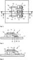
Ein Stiftleiste ist in den Zeichnungen allgemein mit 1 bezeichnet. Diese Stiftleiste 1 dient zum Herstellen einer elektrischen Verbindung bzw. eines elektrischen Anschlusses einer Leiterplatte 2.A header is generally indicated at 1 in the drawings. This
Die Stiftleiste 1 weist bei den Ausführungsbeispielen drei in einer Reihe nebeneinander angeordnete, abgewinkelte Kontaktstifte 3 auf, wobei jeder Kontaktstift 3 einen zur Leiterplatte 2 parallelen ersten Schenkel 4 und einen zur Leiterplatte senkrechten zweiten Schenkel 5 aufweist, wobei die ersten und zweiten Schenkel 4, 5 bogenförmig ineinander übergehen. Die ersten Schenkel 4 können auch geneigt zur Leiterplatte 2 ausgerichtet sein, also nicht rechtwinklig zu den zweiten Schenkeln 5.In the exemplary embodiments, the
Die ersten Schenkel 4 sind in einem Kontaktträger 6 aus einem elektrisch isolierenden Material, vorzugsweise Kunststoff, gehalten und ragen mit ihren freien Steckkontaktenden 4a aus dem Kontaktträger 6 heraus. Die freien tellerförmigen Enden 5a der zweiten Schenkel 5 sind zum Verlöten mit der Leiterplatte 2 ausgebildet, welche nicht dargestellte, gedruckte Leitungen aufweist. Bei der Durchloch-Montage sind die freien Enden 5a natürlich nicht tellerförmig ausgebildet, sondern zum Einstecken in Bohrungen der Leiterplatte 2 geeignet.The
Der Kontaktträger 6 weist beim Ausführungsbeispiel einen balkenförmigen Kopfbereich 7 mit in Montagelage zur Leiterplatte 2 parallelen Durchstecköffnungen 8 für die ersten Schenkel 4 der Kontaktstifte 3 auf. Dieser Kontaktbereich 7 geht in einen in Richtung zu den zweiten Schenkeln 5 der Kontaktstifte 3 versetzten Fußbereich 9 über, welcher Ausnehmungen 10 aufweist, in denen die zweiten Schenkel 5 der Kontaktstifte 3 geführt bzw. gehalten sind. Unterseitig sind an den Fußbereich 9 des Kontaktträgers 6 Standfüße 11 angeformt, welche angrenzend an die freien Enden 5a auf oder in geringem Abstand von der Oberfläche der Leiterplatte 2 enden. Bei der nicht dargestellten Durchloch-Montage liegen sie auf der Leiterplatte 2 auf.In the exemplary embodiment, the
Wesentlich für die Gestaltung der Stiftleiste 1 ist, dass einstückig an den Kontaktträger 6 eine Ansaugplatte 12 für den Saugkopf eines Bestückungsautomaten angeformt ist. Dabei ist die Ansaugplatte 12 so ausgebildet, dass sie die aus dem Kontaktträger 6 bzw. dessen Kopfbereich 7 herausragenden freien Steckkontaktenden 4a der ersten Schenkel 4 wenigstens bereichsweise überdeckt und wenigstens einen, z.B. etwa senkrecht, zur Leiterplatte 2 gerichteten, auf der Leiterplatte 2 aufliegenden Montagesteg 13 aufweist. Vorzugsweise sind zwei Montagestege 13, jeweils einer an einem Seitenrand der Ansaugplatte 12 vorgesehen.It is essential for the design of the
Die Ansaugplatte 12 ist beim Ausführungsbeispiel über zwei Verbindungsstege 14 einstückig mit dem Kontaktträger 6 bzw. dem Kopfbereich 7 des Kontaktträgers 6 verbunden, wobei jeder Verbindungssteg 14 eine Sollbruchstelle 15 aufweist, die z.B. als Einkerbung auf der Unterseite ausgebildet ist (
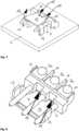
Zur Montage der Stiftleiste 1 wird die Stiftleiste 1 vom Saugkopf eines Bestückungsautomaten an der Ansaugplatte 12 angesaugt und gehalten und an der gewünschten Stelle auf der Leiterplatte 2 abgesetzt. Die Leiterplatte 2 ist zuvor an den entsprechenden Verbindungsstellen mit Lötpaste od. dgl. versehen worden. Die Stiftleiste 1 liegt dabei stabil und lagegerecht mit den Montagestegen 13 und den freien Enden 5a auf der Leiterplatte derart auf, dass die ersten Schenkel 4 parallel zur Leiterplatte 2 ausgerichtet sind.To assemble the
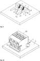
Nach Abschluss des Lötvorganges wird die Ansaugplatte 12 durch Anheben in Richtung des Pfeiles 16 entlang der Sollbruchstellen 15 vom Kontaktträger 6 abgebrochen. Die entsprechenden Bruchstellen sind in
Natürlich ist die Erfindung nicht auf die dargestellten Ausführungsbeispiele beschränkt. Weitere Ausgestaltungen sind möglich, ohne den Grundgedanken zu verlassen. So kann die Stiftleiste 1 auch für die Durchloch-Montage verwendet werden, die Stiftleiste 1 liegt dann mit den Standfüßen 11 auf der Leiterplatte 2 auf.Of course, the invention is not limited to the illustrated embodiments. Further refinements are possible without departing from the basic idea. The
BezugszeichenlisteReference List
- 11
- Stiftleisteheader
- 22
- Leiterplattecircuit board
- 33
- Kontaktstiftcontact pin
- 44
- erster Schenkelfirst leg
- 4a4a
- freies Steckkontaktendefree connector end
- 55
- zweiter Schenkelsecond leg
- 5a5a
- freies Endefree end
- 66
- Kontaktträgercontact carrier
- 77
- Kopfbereichheader area
- 88th
- Durchstecköffnungenthrough openings
- 99
- Fußbereichfooter
- 1010
- Ausnehmungrecess
- 1111
- Standfußstand
- 1212
- Ansaugplatteintake plate
- 1313
- Montagestegassembly bridge
- 1414
- Verbindungsstegconnecting bar
- 1515
- Sollbruchstellepredetermined breaking point
- 1616
- PfeilArrow
- 1717
- Bruchstellebreaking point
- 1818
- SteckerPlug
ZITATE ENTHALTEN IN DER BESCHREIBUNGQUOTES INCLUDED IN DESCRIPTION
Diese Liste der vom Anmelder aufgeführten Dokumente wurde automatisiert erzeugt und ist ausschließlich zur besseren Information des Lesers aufgenommen. Die Liste ist nicht Bestandteil der deutschen Patent- bzw. Gebrauchsmusteranmeldung. Das DPMA übernimmt keinerlei Haftung für etwaige Fehler oder Auslassungen.This list of documents cited by the applicant was generated automatically and is included solely for the better information of the reader. The list is not part of the German patent or utility model application. The DPMA assumes no liability for any errors or omissions.
Zitierte PatentliteraturPatent Literature Cited
- DE 29904493 U1 [0005]DE 29904493 U1 [0005]
Claims (6)
Translated fromGermanPriority Applications (2)
| Application Number | Priority Date | Filing Date | Title |
|---|---|---|---|
| DE202022101142.7UDE202022101142U1 (en) | 2022-03-01 | 2022-03-01 | header |
| DE102023104254.8ADE102023104254A1 (en) | 2022-03-01 | 2023-02-21 | header |
Applications Claiming Priority (1)
| Application Number | Priority Date | Filing Date | Title |
|---|---|---|---|
| DE202022101142.7UDE202022101142U1 (en) | 2022-03-01 | 2022-03-01 | header |
Publications (1)
| Publication Number | Publication Date |
|---|---|
| DE202022101142U1true DE202022101142U1 (en) | 2023-06-02 |
Family
ID=86895373
Family Applications (2)
| Application Number | Title | Priority Date | Filing Date |
|---|---|---|---|
| DE202022101142.7UActiveDE202022101142U1 (en) | 2022-03-01 | 2022-03-01 | header |
| DE102023104254.8APendingDE102023104254A1 (en) | 2022-03-01 | 2023-02-21 | header |
Family Applications After (1)
| Application Number | Title | Priority Date | Filing Date |
|---|---|---|---|
| DE102023104254.8APendingDE102023104254A1 (en) | 2022-03-01 | 2023-02-21 | header |
Country Status (1)
| Country | Link |
|---|---|
| DE (2) | DE202022101142U1 (en) |
Citations (3)
| Publication number | Priority date | Publication date | Assignee | Title |
|---|---|---|---|---|
| DE29904493U1 (en) | 1999-03-11 | 1999-06-10 | Siemens AG, 80333 München | Pin header with angled contact pins that can be mounted on a printed circuit board |
| DE29814935U1 (en) | 1998-08-20 | 2000-01-13 | Robert Bosch Gmbh, 70469 Stuttgart | Power strip for surface mounting on a circuit board |
| DE102006039415A1 (en) | 2006-08-23 | 2008-03-20 | Siemens Ag | Contact strip for use in printed circuit board, has receiving area designed such that contact is movable after attachment to receiving area in its longitudinal direction and/or rotational direction |
- 2022
- 2022-03-01DEDE202022101142.7Upatent/DE202022101142U1/enactiveActive
- 2023
- 2023-02-21DEDE102023104254.8Apatent/DE102023104254A1/enactivePending
Patent Citations (3)
| Publication number | Priority date | Publication date | Assignee | Title |
|---|---|---|---|---|
| DE29814935U1 (en) | 1998-08-20 | 2000-01-13 | Robert Bosch Gmbh, 70469 Stuttgart | Power strip for surface mounting on a circuit board |
| DE29904493U1 (en) | 1999-03-11 | 1999-06-10 | Siemens AG, 80333 München | Pin header with angled contact pins that can be mounted on a printed circuit board |
| DE102006039415A1 (en) | 2006-08-23 | 2008-03-20 | Siemens Ag | Contact strip for use in printed circuit board, has receiving area designed such that contact is movable after attachment to receiving area in its longitudinal direction and/or rotational direction |
Also Published As
| Publication number | Publication date |
|---|---|
| DE102023104254A1 (en) | 2023-09-07 |
Similar Documents
| Publication | Publication Date | Title |
|---|---|---|
| DE102006030135B4 (en) | Device for mounting pins on a printed circuit board | |
| DE1802589A1 (en) | Electrical connection terminal | |
| DE2161871A1 (en) | Socket unit for receiving electronic components | |
| DE2406125B2 (en) | SOCKET CONTACT | |
| DE2833313B1 (en) | Terminal block for printed circuits | |
| DE1269692B (en) | Module arrangement in frame construction for electronic circuits | |
| EP0405416A2 (en) | Multipole connecting device with centering block and shielding arrangement | |
| DE2339681A1 (en) | FASTENING ELEMENT | |
| DE3821411A1 (en) | SWITCH-PLUG COMBINATION FOR PCB | |
| DE3148018C1 (en) | Connection element for chip carriers | |
| DE4324061C2 (en) | Distribution strip | |
| DE1925530A1 (en) | Electrical plug connection | |
| DE202022101142U1 (en) | header | |
| DE4101628A1 (en) | CHIPBOARD BASE | |
| DE2652077C3 (en) | Connection and holding device for platelet-shaped bodies | |
| DE20113884U1 (en) | Electrical connector for a printed circuit board | |
| DD297283A5 (en) | CONTACT HOUSING WITH CONTACT ELEMENTS FOR BROADCASTING | |
| DE19710513A1 (en) | Plug-in card for electronic devices | |
| DE102008046567B3 (en) | Connector for connecting an electrical conductor to a printed circuit board | |
| DE29720511U1 (en) | Installation housing for printed circuit boards and electronic components | |
| DE29919913U1 (en) | Input / output connector | |
| EP0508395B1 (en) | Grounding device | |
| DE10223867B4 (en) | PCB inspection unit | |
| DE1615596A1 (en) | Plug connection for printed circuits | |
| DE19712560C1 (en) | Sub-miniature plug connector e.g. for telecommunications circuit boards |
Legal Events
| Date | Code | Title | Description |
|---|---|---|---|
| R163 | Identified publications notified | ||
| R207 | Utility model specification | ||
| R150 | Utility model maintained after payment of first maintenance fee after three years |