DE202014002841U1 - Contacting arrangement, in particular HF measuring tip - Google Patents
Contacting arrangement, in particular HF measuring tipDownload PDFInfo
- Publication number
- DE202014002841U1 DE202014002841U1DE202014002841.9UDE202014002841UDE202014002841U1DE 202014002841 U1DE202014002841 U1DE 202014002841U1DE 202014002841 UDE202014002841 UDE 202014002841UDE 202014002841 U1DE202014002841 U1DE 202014002841U1
- Authority
- DE
- Germany
- Prior art keywords
- conductor
- contact
- impedance
- carrier
- section
- Prior art date
- Legal status (The legal status is an assumption and is not a legal conclusion. Google has not performed a legal analysis and makes no representation as to the accuracy of the status listed.)
- Expired - Lifetime
Links
- 239000004020conductorSubstances0.000claimsabstractdescription138
- 238000012360testing methodMethods0.000claimsabstractdescription16
- 230000009466transformationEffects0.000claimsdescription15
- 239000004575stoneSubstances0.000claimsdescription7
- WYTGDNHDOZPMIW-RCBQFDQVSA-NalstonineNatural productsC1=CC2=C3C=CC=CC3=NC2=C2N1C[C@H]1[C@H](C)OC=C(C(=O)OC)[C@H]1C2WYTGDNHDOZPMIW-RCBQFDQVSA-N0.000claimsdescription5
- 230000003247decreasing effectEffects0.000claimsdescription2
- 230000008859changeEffects0.000description5
- 239000000523sampleSubstances0.000description5
- 238000005259measurementMethods0.000description3
- 239000002184metalSubstances0.000description3
- 238000010079rubber tappingMethods0.000description3
- 235000012431wafersNutrition0.000description2
- BUHVIAUBTBOHAG-FOYDDCNASA-N(2r,3r,4s,5r)-2-[6-[[2-(3,5-dimethoxyphenyl)-2-(2-methylphenyl)ethyl]amino]purin-9-yl]-5-(hydroxymethyl)oxolane-3,4-diolChemical compoundCOC1=CC(OC)=CC(C(CNC=2C=3N=CN(C=3N=CN=2)[C@H]2[C@@H]([C@H](O)[C@@H](CO)O2)O)C=2C(=CC=CC=2)C)=C1BUHVIAUBTBOHAG-FOYDDCNASA-N0.000description1
- 238000006243chemical reactionMethods0.000description1
- 230000008878couplingEffects0.000description1
- 238000010168coupling processMethods0.000description1
- 238000005859coupling reactionMethods0.000description1
- 230000001419dependent effectEffects0.000description1
- 238000013461designMethods0.000description1
- 238000011161developmentMethods0.000description1
- 230000018109developmental processEffects0.000description1
- RVRCFVVLDHTFFA-UHFFFAOYSA-Nheptasodium;tungsten;nonatriacontahydrateChemical compoundO.O.O.O.O.O.O.O.O.O.O.O.O.O.O.O.O.O.O.O.O.O.O.O.O.O.O.O.O.O.O.O.O.O.O.O.O.O.O.[Na+].[Na+].[Na+].[Na+].[Na+].[Na+].[Na+].[W].[W].[W].[W].[W].[W].[W].[W].[W].[W].[W]RVRCFVVLDHTFFA-UHFFFAOYSA-N0.000description1
- 230000013011matingEffects0.000description1
- 238000000034methodMethods0.000description1
- 230000008569processEffects0.000description1
- 230000003716rejuvenationEffects0.000description1
- 239000004065semiconductorSubstances0.000description1
- 238000000742single-metal depositionMethods0.000description1
- 230000007704transitionEffects0.000description1
Images

Classifications
- G—PHYSICS
- G01—MEASURING; TESTING
- G01R—MEASURING ELECTRIC VARIABLES; MEASURING MAGNETIC VARIABLES
- G01R1/00—Details of instruments or arrangements of the types included in groups G01R5/00 - G01R13/00 and G01R31/00
- G01R1/02—General constructional details
- G01R1/06—Measuring leads; Measuring probes
- G01R1/067—Measuring probes
- G01R1/06772—High frequency probes
- G—PHYSICS
- G01—MEASURING; TESTING
- G01R—MEASURING ELECTRIC VARIABLES; MEASURING MAGNETIC VARIABLES
- G01R1/00—Details of instruments or arrangements of the types included in groups G01R5/00 - G01R13/00 and G01R31/00
- G01R1/02—General constructional details
- G01R1/06—Measuring leads; Measuring probes
- G01R1/067—Measuring probes
- G01R1/06766—Input circuits therefor
- G—PHYSICS
- G01—MEASURING; TESTING
- G01R—MEASURING ELECTRIC VARIABLES; MEASURING MAGNETIC VARIABLES
- G01R15/00—Details of measuring arrangements of the types provided for in groups G01R17/00 - G01R29/00, G01R33/00 - G01R33/26 or G01R35/00
- G01R15/14—Adaptations providing voltage or current isolation, e.g. for high-voltage or high-current networks
- G—PHYSICS
- G01—MEASURING; TESTING
- G01R—MEASURING ELECTRIC VARIABLES; MEASURING MAGNETIC VARIABLES
- G01R31/00—Arrangements for testing electric properties; Arrangements for locating electric faults; Arrangements for electrical testing characterised by what is being tested not provided for elsewhere
- G01R31/28—Testing of electronic circuits, e.g. by signal tracer
Landscapes
- Physics & Mathematics (AREA)
- General Physics & Mathematics (AREA)
- Engineering & Computer Science (AREA)
- General Engineering & Computer Science (AREA)
- Measuring Leads Or Probes (AREA)
- Testing Or Measuring Of Semiconductors Or The Like (AREA)
- Tests Of Electronic Circuits (AREA)
Abstract
Translated fromGermanDescription
Translated fromGermanDie Erfindung betrifft eine Kontaktieranordnung zum Abgreifen und Weiterleiten einer Spannung, insbesondere eine Hochfrequenz-(HF)Messspitze oder HF-Messsonde, mit einem Träger, auf dem eine Leiterstruktur angeordnet ist, wobei die Leiterstruktur an einem kontaktseitigen Ende zumindest ein über einen Rand des Trägers vorstehendes Kontaktelement zum elektrischen Kontaktieren mindestens einer Kontaktstelle eines Prüflings aufweist, und wobei die Leitungsstruktur zumindest einen Impedanzwandler bzw. Impedanz-Transformator aufweist.The invention relates to a Kontaktieranordnung for tapping and forwarding a voltage, in particular a radio frequency (RF) probe or RF probe, with a carrier on which a conductor pattern is arranged, wherein the conductor structure at a contact-side end at least one over an edge of the carrier projecting contact element for electrically contacting at least one contact point of a device under test, and wherein the line structure has at least one impedance transformer or impedance transformer.
Herkömmliche Kontaktieranordnungen in Form von Messspitzen sind u. a. aus der Druckschrift
Wenn allerdings an einem dem kontaktseitigen Ende der Leiterstruktur abgewandten verbindungsseitigen Ende der Leiterstruktur zum Weiterleiten der von dem Prüfling abgegriffenen Signale oder Spannungen ein Koaxialkabel oder eine Schaltung mit einer vorgegebenen Impedanz von bspw. 50 Ω oder ein anderes Anschlusselement mit vorgegebener Impedanz angeschlossen wird, kann es erforderlich werden, einen Impedanzwandler in die Leiterstruktur auf dem Träger einzubauen, so dass die Messspitze ohne unerwünschte Reflexionen zur Vermessung eines Prüflings mit davon abweichender Impedanz verwendet werden kann.However, if a coaxial cable or a circuit having a predetermined impedance of, for example, 50 Ω or another connection element with a predetermined impedance is connected to a connection-side end of the conductor structure remote from the contact-side end of the conductor structure for forwarding the signals or voltages picked up by the test object, it can be necessary to incorporate an impedance converter in the conductor structure on the support, so that the measuring tip can be used without unwanted reflections for measuring a test specimen with deviating impedance.
Als ein solcher Impedanzwandler kommt ein passives Bauteil wie etwa ein RF-Transformator oder ein anderes surface-mounted device SMD in Frage. Ein solcher Impedanzwandler ist jedoch nur zur Impedanz-Transformation über einen eingeschränkten Frequenzbereich verwendbar. Wenn die ausgehend von dem Prüfling durch die Messspitze geleiteten HF-Signale außerhalb dieses Frequenzbands liegen, werden durch den Impedanzwandler unerwünschte Reflexionen erzeugt.As such an impedance converter, a passive device such as an RF transformer or other surface-mounted device SMD may be considered. However, such an impedance converter is usable only for impedance transformation over a limited frequency range. If the RF signals conducted from the test specimen through the probe tip are outside this frequency band, unwanted reflections are produced by the impedance transducer.
In Anbetracht der beschriebenen Probleme ist es die Aufgabe der vorliegenden Erfindung, eine Kontaktieranordnung wie etwa eine HF-Messspitze bereitzustellen, die auch über ein breites Frequenzband die zu vermessenden Signale reflexionsfrei weiterleitet und die besonders flexibel einsetzbar ist.In view of the described problems, it is the object of the present invention to provide a Kontaktieranordnung such as an RF probe tip, which for a wide frequency band, the signal to be measured passes without reflection and is particularly flexible.
Diese Aufgabe wird erfindungsgemäß durch eine Kontaktieranordnung gemäß Anspruch 1 gelöst. Vorteilhafte Weiterbildungen der Erfindung sind in den abhängigen Ansprüchen beschrieben.This object is achieved by a Kontaktieranordnung according to claim 1. Advantageous developments of the invention are described in the dependent claims.
Der Impedanzwandler der erfindungsgemäßen Kontaktieranordnung zeichnet sich dadurch aus, dass er einen elektrischen Leiterabschnitt mit sich allmählich verjüngendem oder erweiterndem Querschnitt aufweist.The impedance converter of the contacting arrangement according to the invention is characterized in that it has an electrical conductor section with a gradually tapered or widening cross section.
Die Erfindung geht auf die Erkenntnis zurück, dass zur Impedanz-Transformation nicht notwendigerweise ein komplexes elektronisches Bauteil wie etwa ein Balun o. dgl. erforderlich ist. Vielmehr genügt es, zur Impedanzwandlung einen Leiterabschnitt mit sich zwischen dem kontaktseitigen Ende und dem verbindungsseitigen Ende der Leiterstruktur allmählich veränderndem Leiterquerschnitt einzusetzen. Die Länge und die Querschnittsänderung dieses Leiterabschnitts sind derart eingerichtet, dass sich der Wellenwiderstand der Leiterstruktur um einen vorgegebenen Wert verändert. Da eine stufige Änderung des Leiterquerschnitts regelmäßig zu Reflexionen führt, erfolgt die Änderung des Leiterquerschnitts erfindungsgemäß bevorzugt allmählich, bevorzugt über eine Wegstrecke von mehr als 5 cm, besonders bevorzugt mehr als 10 cm, insbesondere 20 cm oder mehr.The invention is based on the recognition that for impedance transformation, not necessarily a complex electronic component such as a Balun o. The like. Is required. Rather, it is sufficient for impedance conversion to use a conductor section with gradually changing conductor cross-section between the contact-side end and the connection-side end of the conductor structure. The length and the change in cross section of this conductor section are set up such that the characteristic impedance of the conductor structure changes by a predetermined value. Since a step change in the conductor cross-section regularly leads to reflections, the change in the conductor cross-section is preferably carried out gradually, preferably over a distance of more than 5 cm, more preferably more than 10 cm, in particular 20 cm or more.
Vorzugsweise weist die Leiterstruktur zumindest einen Signalleiter bzw. Spannungsleiter und zumindest einen Masseleiter auf, die jeweils von dem kontaktseitigen Ende zu dem verbindungsseitigen Ende verlaufen, wobei an dem verbindungsseitigen Ende der Leiterstruktur ein Steckverbinder zum Weiterleiten des abgegriffenen Signals angeordnet sein kann. Dabei ist der Leiterabschnitt mit sich veränderndem Querschnitt vorzugsweise in den Signalleiter eingebaut. Der Masseleiter kann ebenso wie der Signalleiter mit einem oder mehreren von dem Träger vorstehenden Kontaktelementen zum elektrischen Kontaktieren mindestens einer Kontaktstelle des Prüflings an dem kontaktseitigen Ende verbunden sein.Preferably, the conductor structure has at least one signal conductor or voltage conductor and at least one ground conductor, which each extend from the contact-side end to the connection-side end, wherein a connector for forwarding the tapped signal can be arranged at the connection-side end of the conductor structure. In this case, the conductor section with a changing cross section is preferably installed in the signal conductor. The ground conductor, like the signal conductor, may be connected to one or more contact elements projecting from the carrier for electrically contacting at least one contact point of the device under test at the contact-side end.
Der Träger kann ein Dielektrikum aufweisen, auf dem die Leiterstruktur angeordnet ist. In einer besonders bevorzugten Ausführungsform der Erfindung ist der Träger in Form einer Leiterplatte gebildet, auf der ein Teil der Leiterstruktur als Leiterbahn aufgebracht ist. In diesem Fall kann der Leiterabschnitt mit sich veränderndem Querschnitt als (im Wesentlichen zweidimensionale, also flächig aufgebrachte) Leiterbahn mit sich verringernder oder vergrößernder Breite gebildet sein. Vorzugsweise ist der Signalleiter zumindest abschnittsweise als Leiterbahn gebildet, während der Masseleiter bspw. als Deckschicht aus einem leitenden Material wie etwa Metall auf einer Rückseite der Leiterplatte angeordnet sein kann.The carrier may comprise a dielectric, on which the conductor structure is arranged. In a particularly preferred embodiment of the Invention, the carrier is formed in the form of a printed circuit board, on which a part of the conductor structure is applied as a conductor track. In this case, the conductor section of varying cross section may be formed as a (substantially two-dimensional, thus applied flat) conductor track with decreasing or increasing width. Preferably, the signal conductor is at least partially formed as a conductor, while the ground conductor, for example, can be arranged as a cover layer of a conductive material such as metal on a back side of the circuit board.
Das Verhältnis zwischen der Leiterbahnbreite an dem einen Ende der Leiterbahn und der Leiterbahnbreite an dem anderen Ende der Leiterbahn ist bevorzugt größer als zwei, besonders bevorzugt größer als drei, insbesondere vier oder mehr. Dieses Verhältnis hängt von der zu erzielenden Impedanz-Transformation ab.The ratio between the track width at the one end of the track and the track width at the other end of the track is preferably greater than two, more preferably greater than three, in particular four or more. This ratio depends on the impedance transformation to be achieved.
Eine zuverlässige und mit einfachen Mitteln erzielbare Impedanz-Transformation auf eine vorgegebene Eingangs- und/oder Ausgangsimpedanz der Leiterstruktur ist dadurch erreichbar, dass der Impedanzwandler eine Klopfenstein-Struktur bzw. einen „Klopfenstein-Taper” umfasst. Durch einen Klopfenstein-Taper werden zwei unterschiedliche vorgegebene Wellenwiderstands-Niveaus durch einen Leiterabschnitt mit sich verjüngendem Querschnitt auf kurzem Weg unter gleichzeitiger Minimierung von Reflexionen miteinander verbunden. Über eine Klopfenstein-Struktur ist eine Impedanz-Transformation über ein besonders breites HF-Frequenzband ohne störende Reflexionen möglich.A reliable and easily achievable impedance transformation to a predetermined input and / or output impedance of the conductor structure is achievable in that the impedance converter comprises a knocking stone structure or a "tapping stone taper". Through a tapping stone taper, two different predetermined wave resistance levels are interconnected by a tapered cross-section conductor section along a short path while minimizing reflections. Over a knocking stone structure, an impedance transformation over a particularly wide RF frequency band is possible without disturbing reflections.
Eine besonders kompakte und kostengünstig herstellbare Kontaktieranordnung kann dadurch bereitgestellt werden, dass der Leiterabschnitt von dem verbindungsseitigen Ende in Richtung auf das kontaktseitige Ende zumindest abschnittsweise kurvig, insbesondere mäanderförmig verläuft. Mit anderen Worten verläuft der sich verjüngende Leiterabschnitt schlangenlinienförmig und weist dabei vorzugsweise mehrere, besonders bevorzugt mehr als fünf, insbesondere sieben oder mehr Krümmungsabschnitte auf, in denen sich die Richtung des Leiterabschnitts um etwa 180° umkehrt. Auf diese Weise kann eine Leiterlänge von bspw. mehr als 30 cm auf einem Trägerbereich einer Länge von bspw. weniger als 10 cm aufgebracht werden. Mit anderen Worten beträgt das Verhältnis zwischen der Länge des Leiterabschnitts und der Längsabmessung des Trägerabschnitts, auf dem der Leiterabschnitt angeordnet ist, drei oder mehr. Die erfindungsgemäße Kontaktieranordnung kann auf besonders einfache Weise dadurch hergestellt werden, dass ein schlangenlinienförmiger Leiterabschnitt in Form einer Leiterbahn auf einer Leiterplatte aufgedruckt oder auf andere Weise aufgebracht wird.A particularly compact and cost-producible contacting arrangement can be provided in that the conductor section extends from the connection-side end in the direction of the contact-side end at least in sections curvy, in particular meandering. In other words, the tapered conductor section runs serpentine and preferably has several, more preferably more than five, in particular seven or more curved sections, in which the direction of the conductor section is reversed by approximately 180 °. In this way, a conductor length of, for example, more than 30 cm can be applied to a carrier region having a length of, for example, less than 10 cm. In other words, the ratio between the length of the conductor portion and the longitudinal dimension of the support portion on which the conductor portion is disposed is three or more. The contacting arrangement according to the invention can be produced in a particularly simple manner in that a serpentine conductor section in the form of a conductor track is printed on a printed circuit board or applied in another way.
Alternativ kann der sich verjüngende Leiterabschnitt auch linear, also ohne Kurven oder Krümmungen, auf dem Träger gebildet sein. Um dennoch zu einer vergleichsweise kompakten Kontaktieranordnung zu kommen, hat es sich als vorteilhaft erwiesen, dass sich der Leiterabschnitt vorzugsweise in Form einer Leiterbahn über mehr als 50%, vorzugsweise über mehr als 80%, insbesondere über die gesamte Abmessung des Trägers von dem kontaktseitigen Ende bis zu dem verbindungsseitigen Ende erstreckt. Diese Abmessung kann vorteilhafterweise mehr als 6 cm und weniger als 20 cm, insbesondere zwischen 10 und 15 cm betragen. Bei einem linear verlaufenden Leiterabschnitt besteht anders als bei einem kurvig verlaufenden Leiterabschnitt nicht die Gefahr eines Übersprechens zwischen einzelnen Leiterschleifen.Alternatively, the tapered conductor section can also be formed linearly, ie without curves or curves, on the carrier. In order nevertheless to achieve a comparatively compact contacting arrangement, it has proved to be advantageous that the conductor section preferably in the form of a conductor track over more than 50%, preferably over more than 80%, in particular over the entire dimension of the carrier from the contact-side end extends to the connection-side end. This dimension may advantageously be more than 6 cm and less than 20 cm, in particular between 10 and 15 cm. In a linearly extending conductor section, unlike a curved conductor section, there is no danger of crosstalk between individual conductor loops.
Dabei hat sich herausgestellt, dass ein einen Klopfenstein-Taper aufweisender Impedanzwandler zur Impedanz-Transformation über einen besonders breiten Frequenzbereich von etwa 700 MHz bis etwa 2,7 GHz, bevorzugt von 500 MHz bis 3 GHz, besonders bevorzugt von 400 MHz bis 10 GHz, insbesondere von 300 MHz bis 20 GHz eingerichtet sein kann, wobei der Reflexionsfaktor T über den gesamten Frequenzbereich kleiner ist als 0,2, insbesondere kleiner ist als 0,1. Im Hinblick auf die üblichen Eingangsimpedanzen von HF-Bauteilen und HF-Leitungen, insbesondere Koaxialleitungen, hat es sich als zweckmäßig herausgestellt, dass das Verhältnis zwischen der Eingangsimpedanz und der Ausgangsimpedanz des Impedanzwandlers bzw. der Leiterstruktur auf 5:1, 1:5, 4:1, 1:4, 2:1 oder 1:2 eingerichtet ist. Unter der Ausgangsimpedanz der Leiterstruktur wird die Impedanz der Leiterstruktur an dem verbindungsseitigen Ende zwischen dem den Leiterabschnitt aufweisenden Signalleiter und einem Masseleiter verstanden (verbindungsseitige Impedanz). Unter der Eingangsimpedanz der Leiterstruktur wird die kontaktseitige Impedanz der Leiterstruktur zwischen dem mit dem Leiterabschnitt verbundenen Kontaktelement und einem mit dem Masseleiter verbundenen Kontaktelement verstanden, die an die Wellenimpedanz des zu vermessenden Prüflings angepasst ist.It has been found that an impedance converter having a knockstone taper for impedance transformation over a particularly wide frequency range from about 700 MHz to about 2.7 GHz, preferably from 500 MHz to 3 GHz, particularly preferably from 400 MHz to 10 GHz, In particular, from 300 MHz to 20 GHz can be set up, wherein the reflection factor T over the entire frequency range is less than 0.2, in particular less than 0.1. With regard to the usual input impedances of RF components and RF lines, in particular coaxial lines, it has proven to be advantageous for the ratio between the input impedance and the output impedance of the impedance converter or the conductor structure to be 5: 1, 1: 5, 4 : 1, 1: 4, 2: 1 or 1: 2 is set up. The output impedance of the conductor pattern is understood to mean the impedance of the conductor pattern at the connection-side end between the signal conductor having the conductor portion and a ground conductor (connection-side impedance). The input impedance of the conductor structure is understood to mean the contact-side impedance of the conductor structure between the contact element connected to the conductor section and a contact element connected to the ground conductor, which is adapted to the wave impedance of the test object to be measured.
Dabei beträgt die kontaktseitige Impedanz der Leiterstruktur vorzugsweise etwa 10 Ω oder etwa 12,5 Ω und/oder die verbindungsseitige Impedanz der Leiterstruktur etwa 50 Ω oder umgekehrt. Im diesem Fall kann ein herkömmliches Koaxialkabel an dem verbindungsseitigen Ende der Kontaktieranordnung angeschlossen werden.In this case, the contact-side impedance of the conductor structure is preferably about 10 Ω or about 12.5 Ω and / or the connection-side impedance of the conductor structure about 50 Ω or vice versa. In this case, a conventional coaxial cable can be connected to the connection-side end of the contacting arrangement.
Im Hinblick auf eine zuverlässige Kontaktierbarkeit der mindestens einen Kontaktstelle des Prüflings ohne die Gefahr einer Beschädigung von Prüfling oder Kontaktelement hat es sich als zweckmäßig erwiesen, dass das mindestens eine Kontaktelement ein vorzugsweise federnd eingerichteter Kontaktfinger ist. Vorzugsweise sind alle Kontaktelemente einschließlich der mit dem Masseleiter verbundenen Massekontaktelemente als federnd eingerichtete Kontaktfinger gebildet.With regard to a reliable contactability of the at least one contact point of the test piece without the risk of damage to the test piece or contact element, it has proved to be expedient that the at least one contact element is a preferably resiliently arranged Contact finger is. Preferably, all contact elements, including the ground contact elements connected to the ground contact elements, are formed as resiliently arranged contact fingers.
Vorzugsweise weist die Kontaktieranordnung zwei, drei, vier, fünf oder mehr, insbesondere sieben, von dem Träger vorstehende Kontaktelemente auf, von denen zumindest ein, insbesondere zwei Kontaktelemente mit mindestens einem an dem Träger angeordneten Masseleiter verbunden sind, der bevorzugt von dem kontaktseitigen Ende zu dem verbindungsseitigen Ende verläuft.The contacting arrangement preferably has two, three, four, five or more, in particular seven, contact elements projecting from the carrier, of which at least one, in particular two contact elements are connected to at least one ground conductor arranged on the carrier, which preferably extends from the contact-side end the connection side end runs.
Die mehreren kontaktfederartig über einen Trägerrand hinausragenden Kontaktelemente können koplanar angeordnet sein, so dass sie zum Kontaktieren von koplanaren Kontaktstellen des Prüflings eingerichtet sind. Vorzugsweise sind zwei äußere Kontaktelemente Massenelemente, die mit dem Masseleiter verbunden sind, während ein mittleres Kontaktelement mit dem Signalleiter verbunden ist, der den sich verjüngenden Leiterabschnitt aufweist. Der gegenseitige Abstand und die Länge der Kontaktelemente sind jeweils derart eingerichtet, dass sich eine vorgegebene Wellenimpedanz an dem kontaktseitigen Ende ergibt, die an die Wellenimpedanz des Prüflings angepasst ist.The plurality of contact spring-like protruding over a support edge contact elements may be arranged coplanar, so that they are adapted to contact coplanar contact points of the specimen. Preferably, two outer contact elements are mass elements connected to the ground conductor, while a middle contact element is connected to the signal conductor having the tapered conductor portion. The mutual distance and the length of the contact elements are each arranged such that a predetermined wave impedance results at the contact-side end, which is adapted to the wave impedance of the test object.
Der mindestens eine Masseleiter kann auf derjenigen Fläche des Trägers angeordnet sein, die der den Leiterabschnitt tragenden Fläche abgewandt ist. Er kann als Metallschicht oder Metalldecke ausgebildet sein, die eine Rückseite des Trägers bedeckt. Alternativ oder zusätzlich kann auch eine Schirmung des Signalleiters der Leiterstruktur vorgesehen sein.The at least one ground conductor can be arranged on that surface of the carrier which is remote from the surface carrying the conductor section. It may be formed as a metal layer or metal ceiling that covers a back of the wearer. Alternatively or additionally, a shielding of the signal conductor of the conductor structure may be provided.
Im Hinblick auf eine Verringerung einer durch die Kontaktieranordnung eingeführten Signalreflexion hat es sich als zweckmäßig erwiesen, dass die von dem Träger vorstehenden Kontaktelemente abwechselnd mit dem Masseleiter und mit dem Leiterabschnitt elektrisch verbunden sind. Eine solche Kontaktelementstruktur kann als GSG-Struktur (Ground-Signal-Ground) bezeichnet werden.With a view to reducing signal reflection introduced by the contacting arrangement, it has been found to be advantageous for the contact elements protruding from the carrier to be electrically connected alternately to the ground conductor and to the conductor section. Such a contact element structure may be referred to as a GSG structure (ground signal ground).
Wie oben bereits erläutert, können durch einen sich abrupt ändernden Leiterquerschnitt Reflexionen eingeführt werden. Eine abrupte Querschnittsänderung bzw. Leiter-Breitenänderung an dem Übergang zwischen der Leiterbahn und dem schmalen Kontaktelement an dem kontaktseitigen Ende der Leiterstruktur kann dadurch verringert werden, dass mehr als zwei, insbesondere drei oder mehr voneinander beabstandete Kontaktelemente mit der Leiterbahn elektrisch verbunden sind. Mit anderen Worten wird die Leiterbahn dadurch aufgefächert, dass sie mit mehr als einem von dem Träger vorstehenden Kontaktelement verbunden ist, wobei zwischen den einzelnen signalführenden Kontaktelementen jeweils ein mit dem Masseleiter verbundenes Massekontaktelement angeordnet sein kann. Auf diese Weise kann die Breite der Leiterbahn an dem kontaktseitigen Ende bis hin zu den Spitzen der Kontaktelemente praktisch fortgeführt werden.As already explained above, reflections can be introduced by an abruptly changing conductor cross-section. An abrupt change in the cross section or conductor width change at the transition between the conductor track and the narrow contact element at the contact-side end of the conductor structure can be reduced by electrically connecting more than two, in particular three or more, spaced-apart contact elements to the conductor track. In other words, the conductor track is fanned out by being connected to more than one contact element projecting from the carrier, wherein in each case one ground contact element connected to the ground conductor can be arranged between the individual signal-carrying contact elements. In this way, the width of the track at the contact-side end to the tips of the contact elements can be practically continued.
Eine abwechselnde Anordnung von Massekontaktelementen und signalführenden Kontaktelementen kann erforderlich sein, da in diesem Fall der Abstand zwischen den einzelnen Kontaktelementen unter Beibehaltung einer niederohmigen Eingangsimpedanz vergrößert werden kann. Wenn bspw. nur ein signalführendes Kontaktelement und ein Massekontaktelement nebeneinander vorhanden sind, ist deren Abstand zur Aufrechterhaltung einer niederohmigen Eingangsimpedanz ggf. auf weniger als 1 μm einzurichten. Ein derart geringer Abstand zwischen zwei Kontaktelementen ist schwierig herstellbar und die entsprechenden Kontaktelemente sind anfällig für Beschädigungen. Wenn andererseits drei oder mehr signalführende Kontaktelemente jeweils zwischen Massekontaktelementen von dem Träger vorstehen, kann ein gegenseitiger Abstand benachbarter Kontaktelemente von mehr als 10 μm ausreichend sein.An alternating arrangement of ground contact elements and signal-carrying contact elements may be required, since in this case the distance between the individual contact elements can be increased while maintaining a low-impedance input impedance. If, for example, only one signal-carrying contact element and one ground contact element are present next to one another, their distance to maintain a low-impedance input impedance may need to be set to less than 1 μm. Such a small distance between two contact elements is difficult to produce and the corresponding contact elements are prone to damage. On the other hand, if three or more signal-carrying contact elements each protrude between ground contact elements of the carrier, a mutual distance of adjacent contact elements of more than 10 microns may be sufficient.
Vorzugsweise sind die beiden äußeren Kontaktelemente Massekontaktelemente, von denen bevorzugt insgesamt vier oder mehr vorhanden sind. Andererseits weist die Kontaktstruktur vorzugsweise drei oder mehr mit der Leiterbahn verbundene signalführende Kontaktelemente auf, die jeweils zwischen zwei Massekontaktelementen vorstehen.Preferably, the two outer contact elements are ground contact elements, of which preferably four or more are present. On the other hand, the contact structure preferably has three or more signal-carrying contact elements connected to the conductor track, which project in each case between two ground contact elements.
Im Hinblick auf eine impedanzangepasste und stabile Ankopplung der erfindungsgemäßen Kontaktieranordnung an ein Verbindungselement wie etwa ein Kabel oder eine elektronische Schaltung kann die Leiterstruktur an dem dem kontaktseitigen Ende abgewandten verbindungsseitigen Ende ein Anschlusselement wie etwa einen Steckverbinder, insbesondere einen Koaxialsteckverbinder aufweisen, wobei bevorzugt ein Masseleiter der Kontaktstruktur mit einem Außenleiter des Steckverbinders und/oder der Leiterabschnitt der Kontaktstruktur mit einem Innenleiter des Steckverbinders verbunden ist.With regard to impedance-matched and stable coupling of the contacting arrangement according to the invention to a connecting element such as a cable or an electronic circuit, the conductor structure may have a connection element such as a connector, in particular a coaxial connector, at the connection-side end facing away from the contact-side end, preferably a ground conductor Contact structure with an outer conductor of the connector and / or the conductor portion of the contact structure is connected to an inner conductor of the connector.
Im Hinblick auf die Anordnung der Kontaktelemente an dem Träger sowie im Hinblick auf die Anschlusselemente und die Verbindung zwischen den Kontaktelementen und den Anschlusselementen wird auf die Druckschrift
Die Erfindung wird im Folgenden anhand der Zeichnung näher erläutert. Diese zeigt inThe invention will be explained in more detail below with reference to the drawing. This shows in
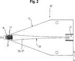
Die aus
Die Leiterstruktur
Von dem kontaktseitigen Ende
An dem verbindungsseitigen Ende
Die Leiterstruktur
Die Kontaktieranordnung
Eine kompaktere Bauweise der Kontaktieranordnung
Erfindungsgemäß erfolgt die Impedanz-Transformation allein durch den Verlauf der Leiterbahn
Anders als die erste Ausführungsform weist die Leiterstruktur
Durch die dargestellte Auffächerung in mehrere mit dem Leiterabschnitt
Im übrigen wird auf die Erläuterungen hinsichtlich der in
BezugszeichenlisteLIST OF REFERENCE NUMBERS
- 10, 10'10, 10 '
- KontaktieranordnungKontaktieranordnung
- 1212
- Träger/LeiterplatteCarrier / circuit board
- 1414
- verbindungsseitiges Endeconnection-side end
- 1616
- kontaktseitiges Endecontact end
- 2020
- Leitungsstrukturmanagement structure
- 2121
- MassekontaktelementeGround contact elements
- 2222
- Kontaktelementecontact elements
- 2323
- federne Kontaktfingerspringy contact fingers
- 2424
- Impedanzwandlerimpedance transformer
- 26, 26'26, 26 '
- Leiterabschnittconductor section
- 27, 27'27, 27 '
- Leiterbahnconductor path
- 4040
- SteckverbinderConnectors
ZITATE ENTHALTEN IN DER BESCHREIBUNG QUOTES INCLUDE IN THE DESCRIPTION
Diese Liste der vom Anmelder aufgeführten Dokumente wurde automatisiert erzeugt und ist ausschließlich zur besseren Information des Lesers aufgenommen. Die Liste ist nicht Bestandteil der deutschen Patent- bzw. Gebrauchsmusteranmeldung. Das DPMA übernimmt keinerlei Haftung für etwaige Fehler oder Auslassungen.This list of the documents listed by the applicant has been generated automatically and is included solely for the better information of the reader. The list is not part of the German patent or utility model application. The DPMA assumes no liability for any errors or omissions.
Zitierte PatentliteraturCited patent literature
- DE 19945178 C2[0002]DE 19945178 C2[0002]
- WO 2006/066676[0002]WO 2006/066676[0002]
- WO 2006/066676 A1[0026]WO 2006/066676 A1[0026]
Claims (13)
Translated fromGermanPriority Applications (9)
| Application Number | Priority Date | Filing Date | Title |
|---|---|---|---|
| DE202014002841.9UDE202014002841U1 (en) | 2014-04-01 | 2014-04-01 | Contacting arrangement, in particular HF measuring tip |
| EP15700416.9AEP3126852B1 (en) | 2014-04-01 | 2015-01-13 | Contacting assembly, in particular an hf measuring tip |
| CA2940904ACA2940904C (en) | 2014-04-01 | 2015-01-13 | Contacting assembly, in particular an hf measuring tip |
| US15/126,897US9804195B2 (en) | 2014-04-01 | 2015-01-13 | HF measuring probe contacting assembly |
| PCT/EP2015/000044WO2015149893A1 (en) | 2014-04-01 | 2015-01-13 | Contacting assembly, in particular an hf measuring tip |
| KR1020167024063AKR20160140606A (en) | 2014-04-01 | 2015-01-13 | Contacting assembly, in particular an HF measuring tip |
| JP2016559930AJP2017516084A (en) | 2014-04-01 | 2015-01-13 | Contact assembly, especially HF measuring tip |
| CN201580017295.6ACN106133531B (en) | 2014-04-01 | 2015-01-13 | Contact arrangement, in particular HF measuring head |
| TW104203134UTWM504245U (en) | 2014-04-01 | 2015-03-03 | Contactor assembly, in particular HF measurement tip |
Applications Claiming Priority (1)
| Application Number | Priority Date | Filing Date | Title |
|---|---|---|---|
| DE202014002841.9UDE202014002841U1 (en) | 2014-04-01 | 2014-04-01 | Contacting arrangement, in particular HF measuring tip |
Publications (1)
| Publication Number | Publication Date |
|---|---|
| DE202014002841U1true DE202014002841U1 (en) | 2014-06-25 |
Family
ID=51163835
Family Applications (1)
| Application Number | Title | Priority Date | Filing Date |
|---|---|---|---|
| DE202014002841.9UExpired - LifetimeDE202014002841U1 (en) | 2014-04-01 | 2014-04-01 | Contacting arrangement, in particular HF measuring tip |
Country Status (9)
| Country | Link |
|---|---|
| US (1) | US9804195B2 (en) |
| EP (1) | EP3126852B1 (en) |
| JP (1) | JP2017516084A (en) |
| KR (1) | KR20160140606A (en) |
| CN (1) | CN106133531B (en) |
| CA (1) | CA2940904C (en) |
| DE (1) | DE202014002841U1 (en) |
| TW (1) | TWM504245U (en) |
| WO (1) | WO2015149893A1 (en) |
Cited By (1)
| Publication number | Priority date | Publication date | Assignee | Title |
|---|---|---|---|---|
| WO2016102172A1 (en)* | 2014-12-22 | 2016-06-30 | Ingun Prüfmittelbau Gmbh | High-frequency test probe |
Families Citing this family (7)
| Publication number | Priority date | Publication date | Assignee | Title |
|---|---|---|---|---|
| GB2546794B (en) | 2016-01-29 | 2020-01-08 | Teraview Ltd | A transmission line |
| CN110297110B (en)* | 2018-03-21 | 2022-02-15 | 科磊股份有限公司 | Probe structure, clamp, containing box, automatic probe replacing system and method |
| TWI665448B (en)* | 2018-07-13 | 2019-07-11 | 中華精測科技股份有限公司 | High frequency probe card device and signal transmission module thereof |
| US11101215B2 (en)* | 2018-09-19 | 2021-08-24 | PsiQuantum Corp. | Tapered connectors for superconductor circuits |
| KR102577446B1 (en) | 2019-02-12 | 2023-09-11 | 삼성전자주식회사 | A test board, a method for fabricating the test board, a device test apparatus using the test board, and a method for fabricating a semiconductor device using the test board |
| DE102020102302A1 (en)* | 2020-01-30 | 2021-08-05 | Ingun Prüfmittelbau Gmbh | High-frequency test contact element and test pin device |
| DE102020119282B4 (en)* | 2020-07-22 | 2022-06-09 | Md Elektronik Gmbh | contact device |
Citations (2)
| Publication number | Priority date | Publication date | Assignee | Title |
|---|---|---|---|---|
| DE19945178C2 (en) | 1999-09-21 | 2003-05-28 | Rosenberger Hochfrequenztech | Measuring tip for high-frequency measurement and method for its production |
| WO2006066676A1 (en) | 2004-12-20 | 2006-06-29 | Rosenberger Hochfrequenztechnik Gmbh & Co. Kg | Measuring tip for measuring high frequency |
Family Cites Families (36)
| Publication number | Priority date | Publication date | Assignee | Title |
|---|---|---|---|---|
| JPS58136108A (en)* | 1982-02-08 | 1983-08-13 | Nec Corp | Meander type transmission line |
| US4697143A (en)* | 1984-04-30 | 1987-09-29 | Cascade Microtech, Inc. | Wafer probe |
| DD278041A3 (en)* | 1987-11-06 | 1990-04-25 | Akad Wissenschaften Ddr | Arrangement for measuring smallest capacity changes |
| US5005932A (en)* | 1989-11-06 | 1991-04-09 | Hughes Aircraft Company | Electro-optic modulator |
| JPH04155261A (en)* | 1990-10-18 | 1992-05-28 | Mitsubishi Electric Corp | ultra high frequency probe needle |
| US5457399A (en)* | 1992-12-14 | 1995-10-10 | Hughes Aircraft Company | Microwave monolithic integrated circuit fabrication, test method and test probes |
| US5561378A (en)* | 1994-07-05 | 1996-10-01 | Motorola, Inc. | Circuit probe for measuring a differential circuit |
| US5506515A (en)* | 1994-07-20 | 1996-04-09 | Cascade Microtech, Inc. | High-frequency probe tip assembly |
| US6229327B1 (en)* | 1997-05-30 | 2001-05-08 | Gregory G. Boll | Broadband impedance matching probe |
| JP3356736B2 (en)* | 1999-11-01 | 2002-12-16 | エヌイーシーワイヤレスネットワークス株式会社 | High frequency probe |
| JP2001244308A (en)* | 2000-02-25 | 2001-09-07 | Mitsubishi Electric Corp | Probe for high frequency signals |
| JP2003087011A (en)* | 2001-06-27 | 2003-03-20 | Murata Mfg Co Ltd | Dielectric duplexer and communication apparatus |
| DE10136726A1 (en)* | 2001-07-27 | 2003-04-03 | Connexion Rosenberger Gmbh | Measuring arrangement for high-frequency measurements with several measuring probes and a method for producing the same |
| US6930497B2 (en)* | 2001-12-19 | 2005-08-16 | Chung Shan Institute Of Science And Technology Armaments Bureau, M.N.D. | Flexible multi-layered probe for measuring a signal from an object |
| DE10217387B4 (en)* | 2002-04-18 | 2018-04-12 | Snaptrack, Inc. | Electrical matching network with a transformation line |
| US6956445B2 (en)* | 2003-02-19 | 2005-10-18 | Electro-Tec Corp. | Broadband high-frequency slip ring system |
| WO2005065258A2 (en)* | 2003-12-24 | 2005-07-21 | Cascade Microtech, Inc. | Active wafer probe |
| DE102004059960A1 (en)* | 2004-12-13 | 2006-06-22 | Bourns, Inc., Riverside | Circuit arrangement for measuring an electric current |
| CN2779421Y (en)* | 2005-01-14 | 2006-05-10 | 廊坊市万科石油天然气技术工程有限公司 | Active transmitting-receiving probe for downfield NMR |
| JP2006317156A (en)* | 2005-05-10 | 2006-11-24 | Matsushita Electric Ind Co Ltd | Vector network analyzer, vector network analyzer calibration method, computer and standard board |
| JP2007010522A (en)* | 2005-06-30 | 2007-01-18 | Matsushita Electric Ind Co Ltd | Through standard board and line standard board |
| CN101336519B (en)* | 2006-01-31 | 2013-09-18 | 艾利森电话股份有限公司 | A method and a system for cable or subscriber loop investigation performing loop topology identification |
| JP2007205995A (en)* | 2006-02-03 | 2007-08-16 | Advanced Systems Japan Inc | High-frequency probe |
| EP1818672B1 (en)* | 2006-02-14 | 2012-08-29 | Mettler-Toledo AG | Measuring device and method for operating the measuring device |
| US7612733B2 (en)* | 2007-03-12 | 2009-11-03 | The Regents Of The University Of Colorado | Transition region for use with an antenna-integrated electron tunneling device and method |
| US8212580B2 (en)* | 2007-04-02 | 2012-07-03 | Google Inc. | Scalable wideband probes, fixtures, and sockets for high speed IC testing and interconnects |
| JP2009014385A (en)* | 2007-07-02 | 2009-01-22 | Si Gijutsu Kenkyusho:Kk | Error reference detector |
| US8134380B2 (en)* | 2008-11-26 | 2012-03-13 | Taiwan Semiconductor Manufacturing Company, Ltd. | Test probe structure |
| DE202009003966U1 (en)* | 2009-03-20 | 2009-06-04 | Rosenberger Hochfrequenztechnik Gmbh & Co. Kg | measuring tips |
| US8928429B2 (en)* | 2011-05-17 | 2015-01-06 | City University Of Hong Kong | Multiple-way ring cavity power combiner and divider |
| CN102411074B (en)* | 2011-08-03 | 2014-10-08 | 广东威特真空电子制造有限公司 | High power waveguide impedance transformer |
| JP5713197B2 (en)* | 2011-09-28 | 2015-05-07 | 株式会社Wave Technology | Balun |
| JP5788767B2 (en)* | 2011-11-07 | 2015-10-07 | 株式会社日本マイクロニクス | Probe block, probe card including the same, and probe device |
| CN102735887B (en)* | 2012-07-16 | 2014-08-27 | 电子科技大学 | Single-ended active probe circuit of digital oscilloscope |
| CN202975125U (en)* | 2012-11-19 | 2013-06-05 | 廊坊霸州供电有限公司 | Auxiliary electricity testing device for grounding |
| CN103235190B (en)* | 2013-04-19 | 2015-10-28 | 重庆金山科技(集团)有限公司 | A kind of impedance test method |
- 2014
- 2014-04-01DEDE202014002841.9Upatent/DE202014002841U1/ennot_activeExpired - Lifetime
- 2015
- 2015-01-13WOPCT/EP2015/000044patent/WO2015149893A1/enactiveApplication Filing
- 2015-01-13KRKR1020167024063Apatent/KR20160140606A/ennot_activeCeased
- 2015-01-13CNCN201580017295.6Apatent/CN106133531B/enactiveActive
- 2015-01-13EPEP15700416.9Apatent/EP3126852B1/enactiveActive
- 2015-01-13CACA2940904Apatent/CA2940904C/enactiveActive
- 2015-01-13USUS15/126,897patent/US9804195B2/enactiveActive
- 2015-01-13JPJP2016559930Apatent/JP2017516084A/enactivePending
- 2015-03-03TWTW104203134Upatent/TWM504245U/ennot_activeIP Right Cessation
Patent Citations (2)
| Publication number | Priority date | Publication date | Assignee | Title |
|---|---|---|---|---|
| DE19945178C2 (en) | 1999-09-21 | 2003-05-28 | Rosenberger Hochfrequenztech | Measuring tip for high-frequency measurement and method for its production |
| WO2006066676A1 (en) | 2004-12-20 | 2006-06-29 | Rosenberger Hochfrequenztechnik Gmbh & Co. Kg | Measuring tip for measuring high frequency |
Cited By (1)
| Publication number | Priority date | Publication date | Assignee | Title |
|---|---|---|---|---|
| WO2016102172A1 (en)* | 2014-12-22 | 2016-06-30 | Ingun Prüfmittelbau Gmbh | High-frequency test probe |
Also Published As
| Publication number | Publication date |
|---|---|
| KR20160140606A (en) | 2016-12-07 |
| CA2940904C (en) | 2020-08-18 |
| JP2017516084A (en) | 2017-06-15 |
| CN106133531B (en) | 2020-10-20 |
| US9804195B2 (en) | 2017-10-31 |
| EP3126852A1 (en) | 2017-02-08 |
| EP3126852B1 (en) | 2019-11-27 |
| US20170153274A1 (en) | 2017-06-01 |
| WO2015149893A1 (en) | 2015-10-08 |
| CA2940904A1 (en) | 2015-10-08 |
| TWM504245U (en) | 2015-07-01 |
| CN106133531A (en) | 2016-11-16 |
Similar Documents
| Publication | Publication Date | Title |
|---|---|---|
| EP3126852B1 (en) | Contacting assembly, in particular an hf measuring tip | |
| EP1780551A1 (en) | Probe assembly with controlled impendance spring pin | |
| DE10002099A1 (en) | Probe tip arrangement in dense pad array, has aggressor conductor located in close proximity to the access transmission line, where redefined capacitance is created between conductor and transmission line | |
| DE10143173A1 (en) | Wafer probe has contact finger array with impedance matching network suitable for wide band | |
| DE202004021093U1 (en) | Differential probe for e.g. integrated circuit, has elongate probing units interconnected to respective active circuits that are interconnected to substrate by respective pair of flexible interconnects | |
| DE102006026229A1 (en) | Probe for e.g. integrated circuit, has contact tips located within periphery of coaxial cable and shielded by ground conductor of coaxial cable, where coaxial cable terminates in oblique terminal section | |
| EP2409166B1 (en) | High frequency measuring probe | |
| DE102005053146A1 (en) | Measuring tip for high-frequency measurement | |
| DE112009005186T5 (en) | SIGNAL DETECTION DEVICES AND CIRCUIT BOARD | |
| DE19945176B4 (en) | Arrangement of spring contacts in a predetermined grid | |
| DE112017007145T5 (en) | BETWEEN PLATE CONNECTION STRUCTURE | |
| WO2013149930A1 (en) | Broadband directional coupler | |
| DE69623921T2 (en) | SURFACE MOUNTED DIRECTIONAL COUPLER | |
| EP3029782A1 (en) | High frequency signalling | |
| DE202004019636U1 (en) | High frequency semiconductor wafer test probe contact unit has coaxial connectors connected to probe tips by matching network and coplanar waveguide | |
| DE112020006584T5 (en) | circuit board and electronic device | |
| DE102020107546A1 (en) | Inspection device | |
| WO2023280582A1 (en) | Test device and method for high-frequency applications | |
| DE102005005751B4 (en) | Test device with reflection-poor signal distribution | |
| DE102020202025A1 (en) | Connection element for the electrical connection of printed circuit boards, connection system and use of a connection element | |
| DE112017007001T5 (en) | BASE PLATINUM MODULE | |
| DE102009048148A1 (en) | Feed forward coupler with strip conductors | |
| DE102004055955B4 (en) | Arrangement for contacting a circuit integrated in a housing | |
| DE202010002527U1 (en) | Measuring arrangement for measuring electronic components with contact arrangement and calibration substrate | |
| DE102017101549B4 (en) | Combined right/left-handed antenna arrangement for an RFID read/write device, RFID read/write device, antenna module for the antenna arrangement and method for operating the antenna arrangement |
Legal Events
| Date | Code | Title | Description |
|---|---|---|---|
| R207 | Utility model specification | Effective date:20140731 | |
| R163 | Identified publications notified | ||
| R163 | Identified publications notified | Effective date:20141113 | |
| R150 | Utility model maintained after payment of first maintenance fee after three years | ||
| R151 | Utility model maintained after payment of second maintenance fee after six years | ||
| R158 | Lapse of ip right after 8 years | ||
| R082 | Change of representative | Representative=s name:KANDLBINDER, MARKUS, DIPL.-PHYS., DE |