DE112018005962T5 - MULTI-ZONE CARRIER HEATING WITHOUT CONTACTS - Google Patents
MULTI-ZONE CARRIER HEATING WITHOUT CONTACTSDownload PDFInfo
- Publication number
- DE112018005962T5 DE112018005962T5DE112018005962.6TDE112018005962TDE112018005962T5DE 112018005962 T5DE112018005962 T5DE 112018005962T5DE 112018005962 TDE112018005962 TDE 112018005962TDE 112018005962 T5DE112018005962 T5DE 112018005962T5
- Authority
- DE
- Germany
- Prior art keywords
- zones
- electrical connections
- carrier base
- base according
- resistance layer
- Prior art date
- Legal status (The legal status is an assumption and is not a legal conclusion. Google has not performed a legal analysis and makes no representation as to the accuracy of the status listed.)
- Pending
Links
Images


Classifications
- H—ELECTRICITY
- H01—ELECTRIC ELEMENTS
- H01L—SEMICONDUCTOR DEVICES NOT COVERED BY CLASS H10
- H01L21/00—Processes or apparatus adapted for the manufacture or treatment of semiconductor or solid state devices or of parts thereof
- H01L21/67—Apparatus specially adapted for handling semiconductor or electric solid state devices during manufacture or treatment thereof; Apparatus specially adapted for handling wafers during manufacture or treatment of semiconductor or electric solid state devices or components ; Apparatus not specifically provided for elsewhere
- H01L21/683—Apparatus specially adapted for handling semiconductor or electric solid state devices during manufacture or treatment thereof; Apparatus specially adapted for handling wafers during manufacture or treatment of semiconductor or electric solid state devices or components ; Apparatus not specifically provided for elsewhere for supporting or gripping
- H01L21/687—Apparatus specially adapted for handling semiconductor or electric solid state devices during manufacture or treatment thereof; Apparatus specially adapted for handling wafers during manufacture or treatment of semiconductor or electric solid state devices or components ; Apparatus not specifically provided for elsewhere for supporting or gripping using mechanical means, e.g. chucks, clamps or pinches
- H01L21/68714—Apparatus specially adapted for handling semiconductor or electric solid state devices during manufacture or treatment thereof; Apparatus specially adapted for handling wafers during manufacture or treatment of semiconductor or electric solid state devices or components ; Apparatus not specifically provided for elsewhere for supporting or gripping using mechanical means, e.g. chucks, clamps or pinches the wafers being placed on a susceptor, stage or support
- H01L21/68785—Apparatus specially adapted for handling semiconductor or electric solid state devices during manufacture or treatment thereof; Apparatus specially adapted for handling wafers during manufacture or treatment of semiconductor or electric solid state devices or components ; Apparatus not specifically provided for elsewhere for supporting or gripping using mechanical means, e.g. chucks, clamps or pinches the wafers being placed on a susceptor, stage or support characterised by the mechanical construction of the susceptor, stage or support
- C—CHEMISTRY; METALLURGY
- C23—COATING METALLIC MATERIAL; COATING MATERIAL WITH METALLIC MATERIAL; CHEMICAL SURFACE TREATMENT; DIFFUSION TREATMENT OF METALLIC MATERIAL; COATING BY VACUUM EVAPORATION, BY SPUTTERING, BY ION IMPLANTATION OR BY CHEMICAL VAPOUR DEPOSITION, IN GENERAL; INHIBITING CORROSION OF METALLIC MATERIAL OR INCRUSTATION IN GENERAL
- C23C—COATING METALLIC MATERIAL; COATING MATERIAL WITH METALLIC MATERIAL; SURFACE TREATMENT OF METALLIC MATERIAL BY DIFFUSION INTO THE SURFACE, BY CHEMICAL CONVERSION OR SUBSTITUTION; COATING BY VACUUM EVAPORATION, BY SPUTTERING, BY ION IMPLANTATION OR BY CHEMICAL VAPOUR DEPOSITION, IN GENERAL
- C23C16/00—Chemical coating by decomposition of gaseous compounds, without leaving reaction products of surface material in the coating, i.e. chemical vapour deposition [CVD] processes
- C23C16/44—Chemical coating by decomposition of gaseous compounds, without leaving reaction products of surface material in the coating, i.e. chemical vapour deposition [CVD] processes characterised by the method of coating
- C23C16/458—Chemical coating by decomposition of gaseous compounds, without leaving reaction products of surface material in the coating, i.e. chemical vapour deposition [CVD] processes characterised by the method of coating characterised by the method used for supporting substrates in the reaction chamber
- C23C16/4582—Rigid and flat substrates, e.g. plates or discs
- C23C16/4583—Rigid and flat substrates, e.g. plates or discs the substrate being supported substantially horizontally
- C23C16/4586—Elements in the interior of the support, e.g. electrodes, heating or cooling devices
- H—ELECTRICITY
- H01—ELECTRIC ELEMENTS
- H01L—SEMICONDUCTOR DEVICES NOT COVERED BY CLASS H10
- H01L21/00—Processes or apparatus adapted for the manufacture or treatment of semiconductor or solid state devices or of parts thereof
- H01L21/67—Apparatus specially adapted for handling semiconductor or electric solid state devices during manufacture or treatment thereof; Apparatus specially adapted for handling wafers during manufacture or treatment of semiconductor or electric solid state devices or components ; Apparatus not specifically provided for elsewhere
- H01L21/67005—Apparatus not specifically provided for elsewhere
- H01L21/67011—Apparatus for manufacture or treatment
- H01L21/67098—Apparatus for thermal treatment
- H01L21/67103—Apparatus for thermal treatment mainly by conduction
- H—ELECTRICITY
- H01—ELECTRIC ELEMENTS
- H01L—SEMICONDUCTOR DEVICES NOT COVERED BY CLASS H10
- H01L21/00—Processes or apparatus adapted for the manufacture or treatment of semiconductor or solid state devices or of parts thereof
- H01L21/67—Apparatus specially adapted for handling semiconductor or electric solid state devices during manufacture or treatment thereof; Apparatus specially adapted for handling wafers during manufacture or treatment of semiconductor or electric solid state devices or components ; Apparatus not specifically provided for elsewhere
- H01L21/67005—Apparatus not specifically provided for elsewhere
- H01L21/67011—Apparatus for manufacture or treatment
- H01L21/67098—Apparatus for thermal treatment
- H01L21/67109—Apparatus for thermal treatment mainly by convection
- H—ELECTRICITY
- H01—ELECTRIC ELEMENTS
- H01L—SEMICONDUCTOR DEVICES NOT COVERED BY CLASS H10
- H01L21/00—Processes or apparatus adapted for the manufacture or treatment of semiconductor or solid state devices or of parts thereof
- H01L21/67—Apparatus specially adapted for handling semiconductor or electric solid state devices during manufacture or treatment thereof; Apparatus specially adapted for handling wafers during manufacture or treatment of semiconductor or electric solid state devices or components ; Apparatus not specifically provided for elsewhere
- H01L21/67005—Apparatus not specifically provided for elsewhere
- H01L21/67242—Apparatus for monitoring, sorting or marking
- H01L21/67248—Temperature monitoring
- H—ELECTRICITY
- H01—ELECTRIC ELEMENTS
- H01L—SEMICONDUCTOR DEVICES NOT COVERED BY CLASS H10
- H01L21/00—Processes or apparatus adapted for the manufacture or treatment of semiconductor or solid state devices or of parts thereof
- H01L21/67—Apparatus specially adapted for handling semiconductor or electric solid state devices during manufacture or treatment thereof; Apparatus specially adapted for handling wafers during manufacture or treatment of semiconductor or electric solid state devices or components ; Apparatus not specifically provided for elsewhere
- H01L21/683—Apparatus specially adapted for handling semiconductor or electric solid state devices during manufacture or treatment thereof; Apparatus specially adapted for handling wafers during manufacture or treatment of semiconductor or electric solid state devices or components ; Apparatus not specifically provided for elsewhere for supporting or gripping
- H01L21/687—Apparatus specially adapted for handling semiconductor or electric solid state devices during manufacture or treatment thereof; Apparatus specially adapted for handling wafers during manufacture or treatment of semiconductor or electric solid state devices or components ; Apparatus not specifically provided for elsewhere for supporting or gripping using mechanical means, e.g. chucks, clamps or pinches
- H01L21/68714—Apparatus specially adapted for handling semiconductor or electric solid state devices during manufacture or treatment thereof; Apparatus specially adapted for handling wafers during manufacture or treatment of semiconductor or electric solid state devices or components ; Apparatus not specifically provided for elsewhere for supporting or gripping using mechanical means, e.g. chucks, clamps or pinches the wafers being placed on a susceptor, stage or support
- H01L21/68735—Apparatus specially adapted for handling semiconductor or electric solid state devices during manufacture or treatment thereof; Apparatus specially adapted for handling wafers during manufacture or treatment of semiconductor or electric solid state devices or components ; Apparatus not specifically provided for elsewhere for supporting or gripping using mechanical means, e.g. chucks, clamps or pinches the wafers being placed on a susceptor, stage or support characterised by edge profile or support profile
- H—ELECTRICITY
- H01—ELECTRIC ELEMENTS
- H01L—SEMICONDUCTOR DEVICES NOT COVERED BY CLASS H10
- H01L21/00—Processes or apparatus adapted for the manufacture or treatment of semiconductor or solid state devices or of parts thereof
- H01L21/67—Apparatus specially adapted for handling semiconductor or electric solid state devices during manufacture or treatment thereof; Apparatus specially adapted for handling wafers during manufacture or treatment of semiconductor or electric solid state devices or components ; Apparatus not specifically provided for elsewhere
- H01L21/683—Apparatus specially adapted for handling semiconductor or electric solid state devices during manufacture or treatment thereof; Apparatus specially adapted for handling wafers during manufacture or treatment of semiconductor or electric solid state devices or components ; Apparatus not specifically provided for elsewhere for supporting or gripping
- H01L21/687—Apparatus specially adapted for handling semiconductor or electric solid state devices during manufacture or treatment thereof; Apparatus specially adapted for handling wafers during manufacture or treatment of semiconductor or electric solid state devices or components ; Apparatus not specifically provided for elsewhere for supporting or gripping using mechanical means, e.g. chucks, clamps or pinches
- H01L21/68714—Apparatus specially adapted for handling semiconductor or electric solid state devices during manufacture or treatment thereof; Apparatus specially adapted for handling wafers during manufacture or treatment of semiconductor or electric solid state devices or components ; Apparatus not specifically provided for elsewhere for supporting or gripping using mechanical means, e.g. chucks, clamps or pinches the wafers being placed on a susceptor, stage or support
- H01L21/68757—Apparatus specially adapted for handling semiconductor or electric solid state devices during manufacture or treatment thereof; Apparatus specially adapted for handling wafers during manufacture or treatment of semiconductor or electric solid state devices or components ; Apparatus not specifically provided for elsewhere for supporting or gripping using mechanical means, e.g. chucks, clamps or pinches the wafers being placed on a susceptor, stage or support characterised by a coating or a hardness or a material
- H—ELECTRICITY
- H01—ELECTRIC ELEMENTS
- H01L—SEMICONDUCTOR DEVICES NOT COVERED BY CLASS H10
- H01L23/00—Details of semiconductor or other solid state devices
- H01L23/48—Arrangements for conducting electric current to or from the solid state body in operation, e.g. leads, terminal arrangements ; Selection of materials therefor
- H01L23/482—Arrangements for conducting electric current to or from the solid state body in operation, e.g. leads, terminal arrangements ; Selection of materials therefor consisting of lead-in layers inseparably applied to the semiconductor body (electrodes)
- H01L23/485—Arrangements for conducting electric current to or from the solid state body in operation, e.g. leads, terminal arrangements ; Selection of materials therefor consisting of lead-in layers inseparably applied to the semiconductor body (electrodes) consisting of layered constructions comprising conductive layers and insulating layers, e.g. planar contacts
- H—ELECTRICITY
- H01—ELECTRIC ELEMENTS
- H01L—SEMICONDUCTOR DEVICES NOT COVERED BY CLASS H10
- H01L23/00—Details of semiconductor or other solid state devices
- H01L23/52—Arrangements for conducting electric current within the device in operation from one component to another, i.e. interconnections, e.g. wires, lead frames
- H01L23/522—Arrangements for conducting electric current within the device in operation from one component to another, i.e. interconnections, e.g. wires, lead frames including external interconnections consisting of a multilayer structure of conductive and insulating layers inseparably formed on the semiconductor body
- H—ELECTRICITY
- H05—ELECTRIC TECHNIQUES NOT OTHERWISE PROVIDED FOR
- H05B—ELECTRIC HEATING; ELECTRIC LIGHT SOURCES NOT OTHERWISE PROVIDED FOR; CIRCUIT ARRANGEMENTS FOR ELECTRIC LIGHT SOURCES, IN GENERAL
- H05B1/00—Details of electric heating devices
- H05B1/02—Automatic switching arrangements specially adapted to apparatus ; Control of heating devices
- H05B1/0202—Switches
- H—ELECTRICITY
- H05—ELECTRIC TECHNIQUES NOT OTHERWISE PROVIDED FOR
- H05B—ELECTRIC HEATING; ELECTRIC LIGHT SOURCES NOT OTHERWISE PROVIDED FOR; CIRCUIT ARRANGEMENTS FOR ELECTRIC LIGHT SOURCES, IN GENERAL
- H05B1/00—Details of electric heating devices
- H05B1/02—Automatic switching arrangements specially adapted to apparatus ; Control of heating devices
- H05B1/0227—Applications
- H05B1/023—Industrial applications
- H05B1/0233—Industrial applications for semiconductors manufacturing
- H—ELECTRICITY
- H05—ELECTRIC TECHNIQUES NOT OTHERWISE PROVIDED FOR
- H05B—ELECTRIC HEATING; ELECTRIC LIGHT SOURCES NOT OTHERWISE PROVIDED FOR; CIRCUIT ARRANGEMENTS FOR ELECTRIC LIGHT SOURCES, IN GENERAL
- H05B3/00—Ohmic-resistance heating
- H05B3/02—Details
- H05B3/06—Heater elements structurally combined with coupling elements or holders
- H—ELECTRICITY
- H05—ELECTRIC TECHNIQUES NOT OTHERWISE PROVIDED FOR
- H05B—ELECTRIC HEATING; ELECTRIC LIGHT SOURCES NOT OTHERWISE PROVIDED FOR; CIRCUIT ARRANGEMENTS FOR ELECTRIC LIGHT SOURCES, IN GENERAL
- H05B3/00—Ohmic-resistance heating
- H05B3/20—Heating elements having extended surface area substantially in a two-dimensional plane, e.g. plate-heater
- H05B3/22—Heating elements having extended surface area substantially in a two-dimensional plane, e.g. plate-heater non-flexible
- H05B3/28—Heating elements having extended surface area substantially in a two-dimensional plane, e.g. plate-heater non-flexible heating conductor embedded in insulating material
- H—ELECTRICITY
- H05—ELECTRIC TECHNIQUES NOT OTHERWISE PROVIDED FOR
- H05B—ELECTRIC HEATING; ELECTRIC LIGHT SOURCES NOT OTHERWISE PROVIDED FOR; CIRCUIT ARRANGEMENTS FOR ELECTRIC LIGHT SOURCES, IN GENERAL
- H05B2203/00—Aspects relating to Ohmic resistive heating covered by group H05B3/00
- H05B2203/002—Heaters using a particular layout for the resistive material or resistive elements
- H05B2203/005—Heaters using a particular layout for the resistive material or resistive elements using multiple resistive elements or resistive zones isolated from each other
- H—ELECTRICITY
- H05—ELECTRIC TECHNIQUES NOT OTHERWISE PROVIDED FOR
- H05B—ELECTRIC HEATING; ELECTRIC LIGHT SOURCES NOT OTHERWISE PROVIDED FOR; CIRCUIT ARRANGEMENTS FOR ELECTRIC LIGHT SOURCES, IN GENERAL
- H05B2203/00—Aspects relating to Ohmic resistive heating covered by group H05B3/00
- H05B2203/002—Heaters using a particular layout for the resistive material or resistive elements
- H05B2203/007—Heaters using a particular layout for the resistive material or resistive elements using multiple electrically connected resistive elements or resistive zones
- H—ELECTRICITY
- H05—ELECTRIC TECHNIQUES NOT OTHERWISE PROVIDED FOR
- H05B—ELECTRIC HEATING; ELECTRIC LIGHT SOURCES NOT OTHERWISE PROVIDED FOR; CIRCUIT ARRANGEMENTS FOR ELECTRIC LIGHT SOURCES, IN GENERAL
- H05B2203/00—Aspects relating to Ohmic resistive heating covered by group H05B3/00
- H05B2203/014—Heaters using resistive wires or cables not provided for in H05B3/54
- H—ELECTRICITY
- H05—ELECTRIC TECHNIQUES NOT OTHERWISE PROVIDED FOR
- H05B—ELECTRIC HEATING; ELECTRIC LIGHT SOURCES NOT OTHERWISE PROVIDED FOR; CIRCUIT ARRANGEMENTS FOR ELECTRIC LIGHT SOURCES, IN GENERAL
- H05B2203/00—Aspects relating to Ohmic resistive heating covered by group H05B3/00
- H05B2203/016—Heaters using particular connecting means
- H—ELECTRICITY
- H05—ELECTRIC TECHNIQUES NOT OTHERWISE PROVIDED FOR
- H05B—ELECTRIC HEATING; ELECTRIC LIGHT SOURCES NOT OTHERWISE PROVIDED FOR; CIRCUIT ARRANGEMENTS FOR ELECTRIC LIGHT SOURCES, IN GENERAL
- H05B2203/00—Aspects relating to Ohmic resistive heating covered by group H05B3/00
- H05B2203/035—Electrical circuits used in resistive heating apparatus
Landscapes
- Engineering & Computer Science (AREA)
- Physics & Mathematics (AREA)
- Condensed Matter Physics & Semiconductors (AREA)
- General Physics & Mathematics (AREA)
- Computer Hardware Design (AREA)
- Microelectronics & Electronic Packaging (AREA)
- Power Engineering (AREA)
- Manufacturing & Machinery (AREA)
- Chemical & Material Sciences (AREA)
- General Chemical & Material Sciences (AREA)
- Chemical Kinetics & Catalysis (AREA)
- Materials Engineering (AREA)
- Mechanical Engineering (AREA)
- Metallurgy (AREA)
- Organic Chemistry (AREA)
- Resistance Heating (AREA)
- Control Of Resistance Heating (AREA)
- Container, Conveyance, Adherence, Positioning, Of Wafer (AREA)
Abstract
Translated fromGermanDescription
Translated fromGermanQUERVERWEIS AUF VERWANDTE ANWENDUNGENCROSS REFERENCE TO RELATED APPLICATIONS
Diese Anmeldung beansprucht die Priorität und den Nutzen der am 21. November 2017 eingereichten vorläufigen
Die vorliegende Erfindung betrifft allgemein Halbleiterverarbeitungsgeräte und im Besonderen Substratträgersockel zum Tragen und Erwärmen eines Substrats, wie beispielsweise eines Wafers, auf diesem.The present invention relates generally to semiconductor processing devices and, more particularly, to substrate support pedestals for supporting and heating a substrate, such as a wafer, thereon.
HINTERGRUNDBACKGROUND
Die Aussagen in diesem Abschnitt liefern lediglich Hintergrundinformationen in Bezug auf die vorliegende Erfindung und stellen möglicherweise keinen Stand der Technik dar.The statements in this section merely provide background information related to the present invention and may not represent prior art.
Eine Wafer-Trägeranordnung, wie beispielsweise ein Sockel für die Halbleiterverarbeitung, ist in einer Halbleiterverarbeitungskammer angeordnet und umfasst typischerweise einen Wafer-Trägerabschnitt und einen Schaft, der an einem zentralen Bereich des Wafer-Trägerabschnitts befestigt ist. Der Wafer-Trägerabschnitt kann ein Widerstandsheizelement zur Erzeugung von Wärme und elektrische Anschlüsse zum Anschluss des Widerstandsheizelements an eine externe Stromquelle umfassen. Die elektrischen Anschlüsse sind angrenzend an den zentralen Bereich des Wafer-Trägerabschnitts angeordnet und erstrecken sich in den Schaft. Das Widerstandsheizelement ist außerhalb des zentralen Bereichs des Wafer-Trägerabschnitts angeordnet, und normalerweise befinden sich in der Nähe des zentralen Schaftbereiches aufgrund der elektrischen Anschlüsse keine Widerstandsheizelemente. Infolgedessen wird ein kalter Bereich typischerweise im zentralen Bereich erzeugt, und die Größe des zentralen Bereichs wird daher relativ klein gestaltet, um die Fläche des kalten Bereichs zu verringern.A wafer carrier assembly, such as a socket for semiconductor processing, is disposed in a semiconductor processing chamber and typically includes a wafer carrier portion and a shaft that is attached to a central area of the wafer carrier portion. The wafer support section may include a resistance heating element for generating heat and electrical connections for connecting the resistance heating element to an external power source. The electrical connections are arranged adjacent to the central region of the wafer carrier section and extend into the shaft. The resistance heating element is located outside the central area of the wafer support section, and normally there are no resistance heating elements near the central shaft area due to the electrical connections. As a result, a cold area is typically created in the central area, and the size of the central area is therefore made relatively small to reduce the area of the cold area.
Die reduzierte Größe des zentralen Bereichs begrenzt jedoch die Anzahl der elektrischen Anschlüsse, die in den zentralen Bereichen angeordnet werden können, und folglich die Anzahl der Heizzonen, die unabhängig voneinander gesteuert werden können. Bedingt durch die Komplexität der Integration von Temperaturfühlern in einen Sockel und einen kalten Bereich in der Nähe des Schaftbereiches ist ein konventioneller Wafer-Trägersockel im Allgemeinen so konfiguriert, dass er nur eine oder zwei Heizzonen aufweist. Bei begrenzten Heizzonen kann ein vorbestimmtes Heizprofil über den Wafer-Trägerabschnitt aufgrund verschiedener Faktoren, die in einer Halbleiterverarbeitungskammer vorhanden sein können, um eine lokale Temperatur des Wafer-Trägerabschnitts zu beeinflussen, nicht bereitgestellt werden.However, the reduced size of the central area limits the number of electrical connections that can be placed in the central areas and consequently the number of heating zones that can be controlled independently. Due to the complexity of integrating temperature sensors into a base and a cold area near the shaft area, a conventional wafer support base is generally configured to have only one or two heating zones. With limited heating zones, a predetermined heating profile over the wafer support section cannot be provided due to various factors that may be present in a semiconductor processing chamber to affect a local temperature of the wafer support section.
Darüber hinaus begrenzt die reduzierte Größe des zentralen Bereichs auch die Anzahl der Temperatursensoren, die zur Überwachung der Temperatur des Wafer-Trägerabschnitts verwendet werden können. Die begrenzte Anzahl von Temperatursensoren erlaubt keine präzise Überwachung der Temperatur des Wafer-Trägerabschnitts. Daher wird typischerweise das Widerstandsheizelement des Wafer-Trägerabschnitts mit Verhältnisregelung (d.h. mit offenem Regelkreis) betrieben.In addition, the reduced size of the central area also limits the number of temperature sensors that can be used to monitor the temperature of the wafer support section. The limited number of temperature sensors does not allow precise monitoring of the temperature of the wafer carrier section. Therefore, the resistance heating element of the wafer support section is typically operated with ratio control (i.e. with an open loop).
ZUSAMMENFASSUNGSUMMARY
In einer Ausführungsform umfasst die vorliegende Erfindung einen Trägersockel, der ein Substrat mit einer oberen Widerstandsschicht, die einen ersten Satz von Zonen definiert, und mit einer unteren Widerstandsschicht, die einen zweiten Satz von Zonen definiert, aufweist. Jede Zone des ersten und zweiten Satzes von Zonen ist mit mindestens zwei elektrischen Anschlüssen aus einer Vielzahl von elektrischen Anschlüssen gekoppelt und weist eine Gesamtzahl von elektrischen Anschlüssen, die kleiner oder gleich einer Gesamtzahl des ersten und zweiten Satzes von Zonen ist, auf.In one embodiment, the present invention includes a carrier base having a substrate with an upper resistance layer defining a first set of zones and a lower resistance layer defining a second set of zones. Each zone of the first and second set of zones is coupled to at least two electrical connections from a plurality of electrical connections and has a total number of electrical connections that is less than or equal to a total number of the first and second set of zones.
In einer Ausführungsform sind mindestens zwei elektrische Anschlüsse aus der Vielzahl der elektrischen Anschlüsse in einem zentralen Bereich von mindestens einer der oberen und unteren Widerstandsschichten angeordnet. Die Mehrzahl der elektrischen Anschlüsse kann die Form von Abschlusspads (termination pads) haben.In one embodiment, at least two electrical connections from the plurality of electrical connections are arranged in a central region of at least one of the upper and lower resistance layers. The majority of the electrical connections can take the form of termination pads.
In einer anderen Ausführungsform werden mindestens zwei Zonen aus mindestens einer aus dem ersten Satz von Zonen und dem zweiten Satz von Zonen mit demselben elektrischen Anschluss aus der Vielzahl der elektrischen Anschlüsse verbunden.In another embodiment, at least two zones from at least one of the first set of zones and the second set of zones are connected to the same electrical connection from the plurality of electrical connections.
In einer weiteren Ausführungsform umfasst der Trägersockel keine Durchkontaktierungen und/oder Leitschichten.In a further embodiment, the carrier base does not comprise any plated-through holes and / or conductive layers.
In noch einer weiteren Ausführungsform weist mindestens eine der oberen und unteren Widerstandsschichten eine oder mehrere der folgenden Konfigurationen auf: eine Zwei-Draht-Heizkonfiguration, eine Matrix-Verdrahtungskonfiguration zum Verbinden der oberen und/oder unteren Widerstandsschicht mit einer externen Stromquelle und eine mehrfache Parallelschaltungskonfiguration zum Verbinden der oberen und/oder unteren Widerstandsschicht mit einer externen Stromquelle.In yet another embodiment, at least one of the upper and lower resistance layers has one or more of the following configurations: a two-wire heating configuration, a matrix wiring configuration for connecting the upper and / or lower resistance layer to an external power source, and a multiple parallel connection configuration for Connect the upper and / or lower resistance layer to an external power source.
In einer weiteren Ausführungsform umfasst der Trägersockel außerdem ein Steuersystem mit einer Vielzahl von Stromrichtern zur Leistungsanpassung an jede Zone des ersten und zweiten Satzes von Zonen der oberen und unteren Widerstandsschicht. In another embodiment, the carrier base also includes a control system having a plurality of power converters for adapting power to each zone of the first and second set of zones of the upper and lower resistance layers.
In einer weiteren Ausführungsform weist ein Trägersockel ein Substrat auf, das eine erste Oberfläche und eine der ersten Oberfläche gegenüberliegende zweite Oberfläche, eine obere Widerstandsschicht, die auf der ersten Oberfläche des Substrats angeordnet ist, und eine untere Widerstandsschicht, die auf der zweiten Oberfläche des Substrats angeordnet ist, auf. Die obere und die untere Widerstandsschicht weisen jeweils einen ersten Satz von Zonen und einen zweiten Satz von Zonen auf. Jede Zone des ersten und zweiten Satzes von Zonen ist mit mindestens zwei elektrischen Anschlüssen aus einer Vielzahl von elektrischen Anschlüssen gekoppelt, und die Anzahl der elektrischen Anschlüsse ist kleiner oder gleich einer Anzahl des ersten und zweiten Satzes von Zonen.In a further embodiment, a carrier base has a substrate which has a first surface and a second surface opposite the first surface, an upper resistance layer which is arranged on the first surface of the substrate, and a lower resistance layer which is on the second surface of the substrate is arranged on. The top and bottom resistive layers each have a first set of zones and a second set of zones. Each zone of the first and second set of zones is coupled to at least two electrical connections from a plurality of electrical connections, and the number of electrical connections is less than or equal to a number of the first and second set of zones.
In einer Ausführungsform umfasst der Trägersockel keine Durchkontaktierungen und/oder Leitschichten.In one embodiment, the carrier base does not comprise any plated-through holes and / or conductive layers.
In einer weiteren Ausführungsform werden mindestens zwei Zonen aus mindestens einer aus dem ersten Satz von Zonen und dem zweiten Satz von Zonen mit demselben elektrischen Anschluss aus der Vielzahl der elektrischen Anschlüsse verbunden.In a further embodiment, at least two zones from at least one of the first set of zones and the second set of zones are connected to the same electrical connection from the plurality of electrical connections.
In einer weiteren Ausführungsform weist mindestens eine der oberen und unteren Widerstandsschichten eine oder mehrere der folgenden Konfigurationen auf: eine Zwei-Draht-Heizkonfiguration, eine Matrix-Verdrahtungskonfiguration zur Verbindung mindestens einer der oberen und unteren Widerstandsschichten mit einer externen Stromquelle und eine mehrfache Parallelschaltungskonfiguration zur Verbindung mindestens einer der oberen und unteren Widerstandsschichten mit einer externen Stromquelle.In a further embodiment, at least one of the upper and lower resistance layers has one or more of the following configurations: a two-wire heating configuration, a matrix wiring configuration for connecting at least one of the upper and lower resistance layers to an external power source and a multiple parallel connection configuration for connection at least one of the upper and lower resistance layers with an external power source.
In einer weiteren Ausführungsform umfasst der Trägersockel außerdem ein Steuersystem mit einer Vielzahl von Stromrichtern zur Leistungsanpassung an jede Zone des ersten und zweiten Satzes von Zonen der oberen und unteren Widerstandsschicht.In another embodiment, the carrier base also includes a control system having a plurality of power converters to match power to each zone of the first and second set of zones of the upper and lower resistive layers.
In einer weiteren Ausführungsform sind mindestens zwei elektrische Anschlüsse aus der Vielzahl der elektrischen Anschlüsse in einem zentralen Bereich von mindestens einer der oberen und unteren Widerstandsschichten angeordnet.In a further embodiment, at least two electrical connections from the plurality of electrical connections are arranged in a central region of at least one of the upper and lower resistance layers.
In noch einer weiteren Ausführungsform ist ein Trägerelement vorgesehen, das eine obere Widerstandsschicht mit mindestens zwei Zonen und eine untere Widerstandsschicht umfasst, die in einer anderen Ebene als die obere Widerstandsschicht angeordnet ist, wobei die untere Widerstandsschicht mindestens zwei Zonen aufweist. Ein Hauptsubstrat ist zwischen der oberen und unteren Widerstandsschicht angeordnet. Mindestens zwei elektrische Anschlüsse aus einer Vielzahl von elektrischen Anschlüssen sind auf derselben Ebene wie mindestens eine der oberen und unteren Widerstandsschicht angeordnet, und jede Zone der oberen und unteren Widerstandsschicht ist mit mindestens zwei elektrischen Anschlüssen aus der Vielzahl von elektrischen Anschlüssen gekoppelt, und eine Anzahl von elektrischen Anschlüssen ist kleiner oder gleich einer Gesamtzahl von Zonen der oberen und unteren Widerstandsschicht.In yet another embodiment, a carrier element is provided which comprises an upper resistance layer with at least two zones and a lower resistance layer which is arranged in a different plane than the upper resistance layer, the lower resistance layer having at least two zones. A main substrate is arranged between the upper and lower resistance layers. At least two electrical connections from a plurality of electrical connections are arranged on the same level as at least one of the upper and lower resistance layers, and each zone of the upper and lower resistance layer is coupled to at least two electrical connections from the plurality of electrical connections, and a number of electrical connections is less than or equal to a total number of zones of the upper and lower resistance layers.
In einer Ausführungsform umfasst der Trägersockel keine Durchkontaktierungen und/oder Leitschichten.In one embodiment, the carrier base does not comprise any plated-through holes and / or conductive layers.
In einer weiteren Ausführungsform weist mindestens eine der oberen und unteren Widerstandsschichten eine oder mehrere der folgenden Konfigurationen auf: eine Zweidraht-Heizkonfiguration, eine Matrix-Verdrahtungskonfiguration zur Verbindung der oberen oder unteren Widerstandsschicht mit einer externen Stromquelle und eine mehrfache Parallelschaltungskonfiguration zur Verbindung der oberen oder unteren Widerstandsschicht mit einer externen Stromquelle.In another embodiment, at least one of the upper and lower resistance layers has one or more of the following configurations: a two-wire heating configuration, a matrix wiring configuration for connecting the upper or lower resistance layer to an external power source, and a multiple parallel connection configuration for connecting the upper or lower Resistance layer with an external power source.
Weitere Anwendungsbereiche werden sich aus der hier gegebenen Beschreibung erschließen. Die Beschreibung und die spezifischen Beispiele dienen lediglich der Veranschaulichung und sind nicht dazu gedacht, den Umfang der vorliegenden Erfindung zu beschränken.Further areas of application will emerge from the description given here. The description and specific examples are illustrative only and are not intended to limit the scope of the present invention.
FigurenlisteFigure list
Die vorliegende Erfindung wird anhand der detaillierten Beschreibung und den beigefügten Figuren nähergehend beschrieben werden, wobei:
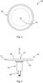
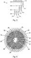
1 eine Draufsicht auf einen Trägersockel, der gemäß den Lehren der vorliegenden Erfindung konstruiert ist, zeigt;2 eine Seitenansicht des Trägersockels von1 zeigt;3 einen Sechs-Zonen-Heizkörper mit vier Anschlussdrähten in Übereinstimmung mit den Lehren der vorliegenden Erfindung darstellt;4 eine obere Widerstandsheizschicht mit sechs Zonen, wobei die Enden der Zonen in Übereinstimmung mit den Lehren der vorliegenden Erfindung in der Mitte eines Substrats verbunden sind, zeigt;5 eine untere Widerstandsheizschicht mit vier Zonen darstellt, wobei die Enden der Zonen in Übereinstimmung mit den Lehren der vorliegenden Erfindung in der Mitte eines Substrats verbunden sind;6 eine Draufsicht auf die obere und untere Widerstandsheizschicht von4 bzw.5 veranschaulicht;7 die Verbindung von Drähten mit Anschlussflächen in der Mitte des Substrats in Übereinstimmung mit den Lehren der vorliegenden Erfindung darstellt;8 eine schematische Darstellung einer Verdrahtungsstruktur zur Steuerung der Widerstandsschicht des Trägersockels aus1 und2 zeigt;9 ein Blockdiagramm eines Regelsystems mit einem Stromrichtersystem in Übereinstimmung mit der Lehre der vorliegenden Erfindung zeigt;10 ein Blockdiagramm eines Stromrichters des Stromrichtersystems in Übereinstimmung mit der Lehre der vorliegenden Erfindung zeigt; und11A ,11B ,11C und11D die Wellenformen unterschiedlicher Ausgangsspannungen des Stromrichters auf der Grundlage unterschiedlicher Eingangsbedingungen in Übereinstimmung mit den Lehren der vorliegenden Erfindung veranschaulichen;
1 Figure 4 shows a top view of a support base constructed in accordance with the teachings of the present invention;2nd a side view of the support base of1 shows;3rd FIG. 6 depicts a six-zone, four-lead radiator in accordance with the teachings of the present invention;4th an upper resistance heating layer with six zones, the ends of the zones in accordance with the teachings of present invention in the middle of a substrate shows;5 represents a lower resistance heating layer with four zones, the ends of the zones being connected in the middle of a substrate in accordance with the teachings of the present invention;6 a plan view of the upper and lower resistance heating layer of4th or.5 illustrated;7 illustrates the connection of wires to pads in the center of the substrate in accordance with the teachings of the present invention;8th is a schematic representation of a wiring structure for controlling the resistance layer of thesupport base 1 and2nd shows;9 Figure 3 shows a block diagram of a control system with a power converter system in accordance with the teachings of the present invention;10th Figure 3 shows a block diagram of a converter of the converter system in accordance with the teachings of the present invention; and11A ,11B ,11C and11D illustrate the waveforms of different converter output voltages based on different input conditions in accordance with the teachings of the present invention;
Gleichlautende Bezugszeichen geben entsprechende Teile in den verschiedenen Ansichten der Figuren an.Identical reference symbols indicate corresponding parts in the different views of the figures.
DETAILLIERTE BESCHREIBUNGDETAILED DESCRIPTION
Die folgende Beschreibung ist lediglich beispielhafter Natur und soll die vorliegende Erfindung, Anwendung oder Verwendung nicht einschränken.The following description is merely exemplary in nature and is not intended to limit the present invention, application, or use.
Gemäß
Bei der Integration von mehr als zwei Heizelementen auf verschiedenen Lagen werden typischerweise eine Leitschicht und Durchkontaktierungen verwendet, um die Heizkreise der Heizelemente im Mittel-/Schachtbereich des Sockels miteinander zu verbinden und abzuschließen. Der Multi-Zonen-Heizsockel
Bezugnehmend auf
Gemäß
Das Widerstandsmaterial des Heizelements kann unter anderem aus hoch TCRgewickelten Drähten, Folien, Dickschicht- oder Dünnschichtmaterialien bestehen. In einer Ausführung sind die Heizelemente in eine Mittelkeramikplatte integriert, die sich im grünen Zustand, teilweise oder vollständig gesintert befinden kann. Diese Heizplatte kann abgedichtet werden, indem ein Rohling oben und unten aufgelegt und durch Diffusionsschweißen oder unterstütztes Heißpress-Sintern vollständig gesintert wird. In einer Ausführung wird der mittlere Anschlussbereich maschinell bearbeitet, und Stifte werden mit den elektrischen Anschlüssen verbunden oder eingelötet (
Der Multi-Zonen-Heizsockel
Entsprechend enthalten die obere Widerstandsschicht
Der Multi-Zonen-Sockel ist dahingehend zu verstehen, dass er nicht auf diese spezifische Struktur, die hier offenbart ist, mit den oberen und unteren Widerstandsschichten
Bezugnehmend auf
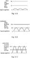
Dies bedeutet, dass die Temperatur der Widerstandsheizelemente
Darüber hinaus sind Matrix- und Multiparallel-Verdrahtungstopologien mit kundenspezifischen Steuerungsalgorithmen integriert. Wie in
In einer Ausgestaltung der vorliegenden Erfindung werden die Widerstandsheizelemente
Im Wesentlichen ist das Steuersystem, das mit dem ersten und zweiten Leitungsdraht in Verbindung steht, so konfiguriert, dass es Änderungen der Spannung zwischen den beiden Leitungsdrähten misst. Genauer gesagt misst das Steuersystem Millivolt (mV)-Änderungen über die Zuleitungsdrähte und verwendet diese Spannungsänderungen dann zur Berechnung einer durchschnittlichen Temperatur des Widerstandsheizelements
Unterschiedliche Heizelemente
Gemäß
Gemäß
Grundsätzlich kann der Abwärtswandler
Der Prozessor
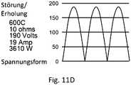
In einer Gestaltung der vorliegenden Erfindung wird eine Eingangsspannung von der Stromquelle
In einer weiteren Ausführungsform der vorliegenden Erfindung bestimmt der Prozessor
Mit dem Stromrichtersystem
Es ist anzumerken, dass die Erfindung nicht auf die in den Beispielen beschriebenen und dar-gestellten Ausführungsformen beschränkt ist. Eine große Anzahl von Weiterbildungen wurde beschrieben und weitere mögliche sind Teil des Wissens des Fachmanns. Diese und weitere Weiterbildungen sowie jeglicher Ersatz durch technische Äquivalente in der Beschreibung und den Figuren führen nicht aus dem Schutzbereich der Erfindung und des vorliegenden Patents heraus.It should be noted that the invention is not limited to those described and illustrated in the examples. presented embodiments is limited. A large number of training courses have been described and other possible ones are part of the knowledge of the person skilled in the art. These and further developments as well as any replacement by technical equivalents in the description and the figures do not lead out of the scope of protection of the invention and the present patent.
ZITATE ENTHALTEN IN DER BESCHREIBUNG QUOTES INCLUDE IN THE DESCRIPTION
Diese Liste der vom Anmelder aufgeführten Dokumente wurde automatisiert erzeugt und ist ausschließlich zur besseren Information des Lesers aufgenommen. Die Liste ist nicht Bestandteil der deutschen Patent- bzw. Gebrauchsmusteranmeldung. Das DPMA übernimmt keinerlei Haftung für etwaige Fehler oder Auslassungen.This list of documents listed by the applicant has been generated automatically and is only included for the better information of the reader. The list is not part of the German patent or utility model application. The DPMA assumes no liability for any errors or omissions.
Zitierte PatentliteraturPatent literature cited
- US 62589023 [0001]US 62589023 [0001]
- US 9196513 [0027]US 9196513 [0027]
- US 9123755 [0036]US 9123755 [0036]
- US 7196295 [0037]US 7196295 [0037]
- US 15624060 [0042]US 15624060 [0042]
- US 7257464 [0044]US 7257464 [0044]
- US 8423193 [0044]US 8423193 [0044]
Claims (15)
Translated fromGermanApplications Claiming Priority (3)
| Application Number | Priority Date | Filing Date | Title |
|---|---|---|---|
| US201762589023P | 2017-11-21 | 2017-11-21 | |
| US62/589,023 | 2017-11-21 | ||
| PCT/US2018/062055WO2019104060A1 (en) | 2017-11-21 | 2018-11-20 | Multi-zone pedestal heater without vias |
Publications (1)
| Publication Number | Publication Date |
|---|---|
| DE112018005962T5true DE112018005962T5 (en) | 2020-08-06 |
Family
ID=64755708
Family Applications (2)
| Application Number | Title | Priority Date | Filing Date |
|---|---|---|---|
| DE112018005962.6TPendingDE112018005962T5 (en) | 2017-11-21 | 2018-11-20 | MULTI-ZONE CARRIER HEATING WITHOUT CONTACTS |
| DE112018005969.3TActiveDE112018005969T8 (en) | 2017-11-21 | 2018-11-20 | Multi-zone support base heater with a conductive layer |
Family Applications After (1)
| Application Number | Title | Priority Date | Filing Date |
|---|---|---|---|
| DE112018005969.3TActiveDE112018005969T8 (en) | 2017-11-21 | 2018-11-20 | Multi-zone support base heater with a conductive layer |
Country Status (7)
| Country | Link |
|---|---|
| US (4) | US11382180B2 (en) |
| JP (2) | JP7303820B2 (en) |
| KR (2) | KR102613392B1 (en) |
| CN (2) | CN212542359U (en) |
| DE (2) | DE112018005962T5 (en) |
| TW (2) | TWI710053B (en) |
| WO (2) | WO2019104048A1 (en) |
Families Citing this family (11)
| Publication number | Priority date | Publication date | Assignee | Title |
|---|---|---|---|---|
| US10764966B2 (en)* | 2016-05-10 | 2020-09-01 | Lam Research Corporation | Laminated heater with different heater trace materials |
| US10667379B2 (en)* | 2016-05-10 | 2020-05-26 | Lam Research Corporation | Connections between laminated heater and heater voltage inputs |
| JP7657780B2 (en)* | 2019-09-12 | 2025-04-07 | ワットロー・エレクトリック・マニュファクチャリング・カンパニー | Ceramic heater and method for forming using liquid phase diffusion bonding |
| US11551951B2 (en)* | 2020-05-05 | 2023-01-10 | Applied Materials, Inc. | Methods and systems for temperature control for a substrate |
| CN113823582A (en)* | 2020-06-21 | 2021-12-21 | 拓荆科技股份有限公司 | Apparatus, system, and method for processing station impedance adjustment |
| CN114496693B (en)* | 2020-11-11 | 2025-09-09 | 中微半导体设备(上海)股份有限公司 | Multi-zone heating device, lower electrode assembly, plasma processing device and temperature adjusting method |
| USD1066620S1 (en)* | 2021-02-12 | 2025-03-11 | Applied Materials, Inc. | Patterned heater pedestal with groove extensions |
| US20230110307A1 (en)* | 2021-10-08 | 2023-04-13 | Watlow Electric Manufacturing Company | Shaped electrical interconnections for multi-layer heater constructions |
| JP2025505742A (en)* | 2022-02-15 | 2025-02-28 | ワットロー・エレクトリック・マニュファクチャリング・カンパニー | Solid-state bonding method for the fabrication of semiconductor chucks and heaters |
| US20250299983A1 (en)* | 2024-03-19 | 2025-09-25 | Tokyo Electron Limited | Ceramic heater assembly with internal and external heating functionality useful in the fabrication of microelectronic devices |
| KR102842210B1 (en)* | 2024-08-01 | 2025-08-01 | 삼성전자주식회사 | Substrate Processing Apparatus |
Citations (4)
| Publication number | Priority date | Publication date | Assignee | Title |
|---|---|---|---|---|
| US7196295B2 (en) | 2003-11-21 | 2007-03-27 | Watlow Electric Manufacturing Company | Two-wire layered heater system |
| US7257464B2 (en) | 2002-08-21 | 2007-08-14 | Watlow Electric Manufacturing Co. | Variable wattage control system |
| US8423193B2 (en) | 2003-08-20 | 2013-04-16 | Watlow Electric Manufacturing Company | Variable wattage control system |
| US9123755B2 (en) | 2011-08-30 | 2015-09-01 | Watlow Electric Manufacturing Company | System and method for controlling a thermal array |
Family Cites Families (36)
| Publication number | Priority date | Publication date | Assignee | Title |
|---|---|---|---|---|
| JP4503714B2 (en) | 1996-09-23 | 2010-07-14 | アプライド マテリアルズ インコーポレイテッド | High temperature resistance heater |
| US6066836A (en) | 1996-09-23 | 2000-05-23 | Applied Materials, Inc. | High temperature resistive heater for a process chamber |
| US6423949B1 (en) | 1999-05-19 | 2002-07-23 | Applied Materials, Inc. | Multi-zone resistive heater |
| US6617553B2 (en) | 1999-05-19 | 2003-09-09 | Applied Materials, Inc. | Multi-zone resistive heater |
| JP2001102157A (en)* | 1999-10-01 | 2001-04-13 | Ngk Insulators Ltd | Ceramic heater |
| JP4028149B2 (en)* | 2000-02-03 | 2007-12-26 | 日本碍子株式会社 | Heating device |
| EP1346607B1 (en) | 2000-11-29 | 2012-07-25 | Thermoceramix, LLC | Resistive heaters and uses thereof |
| KR100434487B1 (en) | 2001-01-17 | 2004-06-05 | 삼성전자주식회사 | Shower head & film forming apparatus having the same |
| JP3897563B2 (en) | 2001-10-24 | 2007-03-28 | 日本碍子株式会社 | Heating device |
| JP2004296254A (en)* | 2003-03-27 | 2004-10-21 | Sumitomo Electric Ind Ltd | Ceramic heater and semiconductor or liquid crystal manufacturing apparatus equipped with the same |
| JP4761723B2 (en)* | 2004-04-12 | 2011-08-31 | 日本碍子株式会社 | Substrate heating device |
| JP2006222008A (en)* | 2005-02-14 | 2006-08-24 | Kyocera Corp | Ceramic heater and electronic components with built-in heater |
| JP2006229040A (en) | 2005-02-18 | 2006-08-31 | Matsushita Electric Ind Co Ltd | Heat treatment method and heat treatment apparatus |
| US9892941B2 (en) | 2005-12-01 | 2018-02-13 | Applied Materials, Inc. | Multi-zone resistive heater |
| JP5202175B2 (en) | 2008-08-07 | 2013-06-05 | 日本碍子株式会社 | Heater with shaft |
| WO2010090948A1 (en) | 2009-02-04 | 2010-08-12 | Mattson Technology, Inc. | Electrostatic chuck system and process for radially tuning the temperature profile across the surface of a substrate |
| US8637794B2 (en)* | 2009-10-21 | 2014-01-28 | Lam Research Corporation | Heating plate with planar heating zones for semiconductor processing |
| US8791392B2 (en)* | 2010-10-22 | 2014-07-29 | Lam Research Corporation | Methods of fault detection for multiplexed heater array |
| US8546732B2 (en)* | 2010-11-10 | 2013-10-01 | Lam Research Corporation | Heating plate with planar heater zones for semiconductor processing |
| US8371567B2 (en) | 2011-04-13 | 2013-02-12 | Novellus Systems, Inc. | Pedestal covers |
| US8624168B2 (en)* | 2011-09-20 | 2014-01-07 | Lam Research Corporation | Heating plate with diode planar heater zones for semiconductor processing |
| US9324589B2 (en)* | 2012-02-28 | 2016-04-26 | Lam Research Corporation | Multiplexed heater array using AC drive for semiconductor processing |
| US8809747B2 (en)* | 2012-04-13 | 2014-08-19 | Lam Research Corporation | Current peak spreading schemes for multiplexed heated array |
| US9089007B2 (en)* | 2012-04-27 | 2015-07-21 | Applied Materials, Inc. | Method and apparatus for substrate support with multi-zone heating |
| US9538583B2 (en)* | 2013-01-16 | 2017-01-03 | Applied Materials, Inc. | Substrate support with switchable multizone heater |
| JP6441927B2 (en) | 2013-08-06 | 2018-12-19 | アプライド マテリアルズ インコーポレイテッドApplied Materials,Incorporated | Multi-zone substrate support heated locally |
| WO2016069808A1 (en)* | 2014-10-31 | 2016-05-06 | Watlow Electric Manufacturing Company | Thermal dynamic response sensing systems for heaters |
| JP2017029876A (en) | 2015-07-29 | 2017-02-09 | 寿典 幕田 | Hollow particle made from bubbles and method for producing the same |
| JP6129451B1 (en)* | 2015-08-20 | 2017-05-17 | 日本碍子株式会社 | Electrostatic chuck heater |
| US9826574B2 (en)* | 2015-10-28 | 2017-11-21 | Watlow Electric Manufacturing Company | Integrated heater and sensor system |
| US10707110B2 (en)* | 2015-11-23 | 2020-07-07 | Lam Research Corporation | Matched TCR joule heater designs for electrostatic chucks |
| US9812342B2 (en)* | 2015-12-08 | 2017-11-07 | Watlow Electric Manufacturing Company | Reduced wire count heater array block |
| KR102552450B1 (en) | 2015-12-28 | 2023-07-05 | 엔지케이 인슐레이터 엘티디 | Disc Heater and Heater Cold Plate Assemblies |
| JP6530333B2 (en)* | 2016-02-29 | 2019-06-12 | 日本特殊陶業株式会社 | Heating member and electrostatic chuck |
| WO2019104040A1 (en)* | 2017-11-21 | 2019-05-31 | Watlow Electric Manufacturing Company | Dual-purpose vias for use in ceramic pedestals |
| US11562913B2 (en)* | 2019-04-25 | 2023-01-24 | Watlow Electric Manufacturing Company | Multi-zone azimuthal heater |
- 2018
- 2018-11-20JPJP2020545074Apatent/JP7303820B2/enactiveActive
- 2018-11-20KRKR1020207017915Apatent/KR102613392B1/enactiveActive
- 2018-11-20DEDE112018005962.6Tpatent/DE112018005962T5/enactivePending
- 2018-11-20WOPCT/US2018/062036patent/WO2019104048A1/ennot_activeCeased
- 2018-11-20KRKR1020207017708Apatent/KR102664620B1/enactiveActive
- 2018-11-20WOPCT/US2018/062055patent/WO2019104060A1/ennot_activeCeased
- 2018-11-20JPJP2020545073Apatent/JP7349439B2/enactiveActive
- 2018-11-20USUS16/196,699patent/US11382180B2/enactiveActive
- 2018-11-20USUS16/196,820patent/US11343879B2/enactiveActive
- 2018-11-20CNCN201890001476.9Upatent/CN212542359U/enactiveActive
- 2018-11-20CNCN201890001471.6Upatent/CN212365925U/enactiveActive
- 2018-11-20DEDE112018005969.3Tpatent/DE112018005969T8/enactiveActive
- 2018-11-21TWTW107141512Apatent/TWI710053B/enactive
- 2018-11-21TWTW107141516Apatent/TWI756494B/enactive
- 2022
- 2022-03-16USUS17/696,486patent/US12127310B2/enactiveActive
- 2022-06-06USUS17/832,890patent/US11895741B2/enactiveActive
Patent Citations (5)
| Publication number | Priority date | Publication date | Assignee | Title |
|---|---|---|---|---|
| US7257464B2 (en) | 2002-08-21 | 2007-08-14 | Watlow Electric Manufacturing Co. | Variable wattage control system |
| US8423193B2 (en) | 2003-08-20 | 2013-04-16 | Watlow Electric Manufacturing Company | Variable wattage control system |
| US7196295B2 (en) | 2003-11-21 | 2007-03-27 | Watlow Electric Manufacturing Company | Two-wire layered heater system |
| US9123755B2 (en) | 2011-08-30 | 2015-09-01 | Watlow Electric Manufacturing Company | System and method for controlling a thermal array |
| US9196513B2 (en) | 2011-08-30 | 2015-11-24 | Watlow Electric Manufacturing Company | System and method for controlling a thermal array |
Also Published As
| Publication number | Publication date |
|---|---|
| JP2021504971A (en) | 2021-02-15 |
| US12127310B2 (en) | 2024-10-22 |
| KR20200086357A (en) | 2020-07-16 |
| JP2021504925A (en) | 2021-02-15 |
| JP7349439B2 (en) | 2023-09-22 |
| TW201926540A (en) | 2019-07-01 |
| WO2019104048A1 (en) | 2019-05-31 |
| TWI756494B (en) | 2022-03-01 |
| TW201926539A (en) | 2019-07-01 |
| US11382180B2 (en) | 2022-07-05 |
| KR102613392B1 (en) | 2023-12-14 |
| KR102664620B1 (en) | 2024-05-14 |
| US20190159291A1 (en) | 2019-05-23 |
| WO2019104060A1 (en) | 2019-05-31 |
| CN212542359U (en) | 2021-02-12 |
| CN212365925U (en) | 2021-01-15 |
| US11895741B2 (en) | 2024-02-06 |
| DE112018005969T5 (en) | 2020-08-06 |
| JP7303820B2 (en) | 2023-07-05 |
| TWI710053B (en) | 2020-11-11 |
| US20220210873A1 (en) | 2022-06-30 |
| KR20200087852A (en) | 2020-07-21 |
| US20220338305A1 (en) | 2022-10-20 |
| US11343879B2 (en) | 2022-05-24 |
| DE112018005969T8 (en) | 2021-03-11 |
| US20190153598A1 (en) | 2019-05-23 |
Similar Documents
| Publication | Publication Date | Title |
|---|---|---|
| DE112018005962T5 (en) | MULTI-ZONE CARRIER HEATING WITHOUT CONTACTS | |
| EP0471171A2 (en) | Device for regulating and limiting the power of a heating plate of ceramic or similar material | |
| DE19631477A1 (en) | Adjustable voltage divider arrangement manufactured in hybrid technology | |
| DE112011104403T5 (en) | Semiconductor pressure sensor | |
| DE102018131999A1 (en) | POWER MODULE AND POWER CONVERTER | |
| DE2400219A1 (en) | ELECTRONIC THERMOSTAT | |
| DE102016214132A1 (en) | Transistor element and semiconductor device | |
| DE102011076651A1 (en) | Current regulation with thermally matched resistors | |
| WO2009141347A1 (en) | Operating temperature measurement for an mos power component, and mos component for carrying out the method | |
| WO2013013781A1 (en) | Individual cell, in particular for a rechargeable battery, rechargeable battery and method for heating an individiual cell, as required | |
| DE102019217690A1 (en) | Heating module | |
| DE69736102T2 (en) | Integrated semiconductor circuit with a thermistor for temperature compensation and its manufacturing method | |
| DE102008057607B4 (en) | Thermoelectric power measuring cell and corresponding measuring method | |
| DE69605611T2 (en) | Thermal head and control circuit therefor | |
| DE102014103513B4 (en) | CIRCUIT ARRANGEMENT AND METHOD FOR OPERATING AN ANALOG DIGITAL CONVERTER | |
| DE202010017531U1 (en) | Device for applying a voltage to a plurality of silicon rods in a CVD reactor | |
| DE112018006693T5 (en) | Semiconductor device | |
| EP3149748A1 (en) | Electronic component | |
| DE102007054541A1 (en) | Flat structure for vehicle seat, has electrical conducting upper layer, electrical conducting lower layer and connecting element is formed as bending threads, where has thread core is provided with coating of semiconducting material | |
| DE112022003359T5 (en) | TEMPERATURE SENSOR INTEGRATED IN A TRANSISTOR ARRAY | |
| EP0396556B1 (en) | Heatable pane of glass | |
| EP0465714B1 (en) | Bow-shaped soldering tip made of ceramic | |
| DE102019219402A1 (en) | Semiconductor device | |
| DE112018005050T5 (en) | SEMICONDUCTOR DEVICE | |
| DE102023002092B4 (en) | INTEGRATED CIRCUIT WITH AN INTEGRATED RESISTOR WITH CURRENT SENSING FUNCTIONALITY |
Legal Events
| Date | Code | Title | Description |
|---|---|---|---|
| R012 | Request for examination validly filed |